

HP INA-30311-TR1, INA-30311-BLK Datasheet
1 GHz Low Noise Silicon MMIC
Amplifier
Technical Data
INA-30311
Features
• Internally Biased, Single 3 V
Supply (6 mA)
• 3.5 dB NF
• 13 dB Gain
• Unconditionally Stable
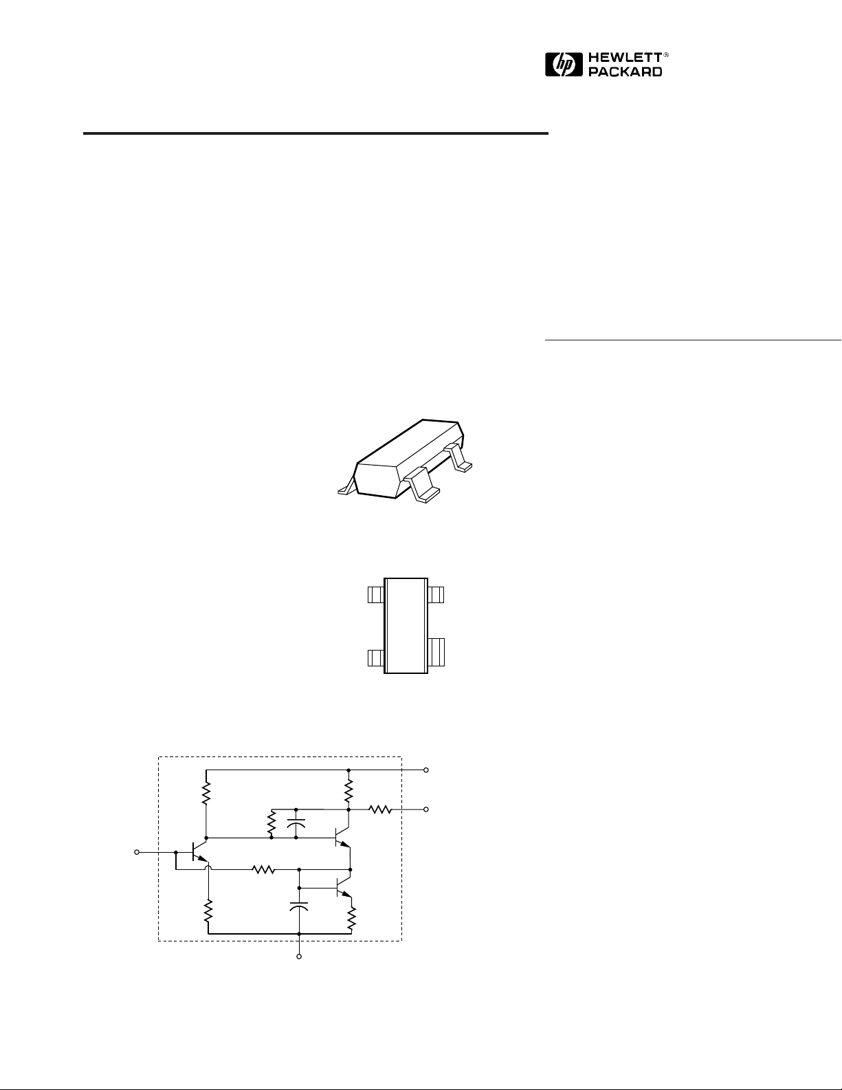
SOT-143 Surface Mount Package
Applications
• LNA or IF Amplifier for
Cellular, Cordless, Special
Mobile Radio, PCS, ISM, and
Wireless LAN Applications
Pin Connections and Package Marking
Equivalent Circuit (Simplified)
INPUT
V
CC
N30
V
CC
GND
OUTPUT
Description
Hewlett-Packard’s INA-30311 is a
Silicon monolithic amplifier for
applications to 1.0 GHz. Packaged
in a miniature SOT-143 package,
it requires very little board space.
The INA-30311 uses an internally
biased topology which eliminates
the need for external components
and provides decreased sensitivity to ground inductance.
The INA-30311 is designed with
an output impedance that varies
from near 200 Ω at low
frequencies to near 50 Ω at higher
frequencies. This provides a
matching advantage for IF
circuits, as well as improved
power efficiency, making it
suitable for battery powered
designs.
RF
INPUT
5963-6679E
GROUND
RF
OUTPUT
6-140
The INA-30311 is fabricated using
HP’s 30 GHz f
Silicon bipolar process which
uses nitride self-alignment submicrometer lithography, trench
isolation, ion implantation, gold
metallization, and polyimide
intermetal dielectric and scratch
protection to achieve superior
performance, uniformity, and
reliability.
MAX
ISOSAT
TM
Absolute Maximum Ratings
Absolute
Symbol Parameter Units Maximum
V
CC
P
in
T
j
T
STG
Device Voltage, to ground V 12
CW RF Input Power dBm +13
Junction Temperature °C 150
Storage Temperature °C -65 to 150
[1]
Thermal Resistance
θ
= 550°C/W
j-c
Notes:
1. Operation of this device above any one
of these limits may cause permanent
damage.
2. T
= 25°C (T
C
temperature at the package pins where
contact is made to the circuit board).
is defined to be the
C
[2]
:
INA-30311 Electrical Specifications
[3]
, T
= 25°C, ZO = 50 Ω, V
C
CC
= 3 V
Symbol Parameters and Test Conditions Units Min. Typ. Max.
G
p
Power Gain (|S21|2) f = 900 MHz dB 11 13
NF Noise Figure f = 900 MHz dB 3.5
P
1dB
IP
3
Output Power at 1 dB Gain Compression f = 900 MHz dBm -11
Third Order Intercept Point f = 900 MHz dBm -2
VSWR Input VSWR f = 900 MHz 1.7
I
cc
ι
d
INA-30311 Typical Scattering Parameters
Freq. S
Device Current mA 6.3 7.5
Group Delay f = 900 MHz ps 325
[3]
, T
11
= 25°C, ZO = 50 Ω, V
C
S
21
S
12
CC
= 3 V
S
22
GHz Mag Ang dB Mag Ang dB Mag Ang Mag Ang Factor
0.05 0.09 -1 16.12 6.40 -6 -38.1 0.012 2 0.57 -1 4.35
0.10 0.09 -2 16.11 6.39 -12 -38.2 0.012 4 0.56 -3 4.43
0.20 0.10 -6 16.12 6.40 -25 -38.4 0.012 8 0.56 -7 4.41
0.30 0.13 -16 16.14 6.41 -38 -38.9 0.011 13 0.55 -11 4.83
0.40 0.16 -29 16.07 6.36 -52 -39.4 0.011 19 0.54 -14 4.88
0.50 0.18 -42 15.90 6.24 -66 -40.1 0.010 27 0.52 -18 5.60
0.60 0.21 -59 15.56 6.00 -81 -40.7 0.009 40 0.50 -20 6.58
0.70 0.22 -75 15.04 5.65 -95 -40.7 0.009 57 0.47 -23 7.26
0.80 0.24 -92 14.34 5.21 -109 -39.6 0.011 74 0.46 -24 6.49
0.90 0.25 -107 13.44 4.70 -122 -37.6 0.013 86 0.44 -24 6.23
1.00 0.26 -122 12.53 4.23 -135 -35.5 0.017 94 0.43 -25 5.35
1.20 0.27 -144 10.50 3.35 -155 -32.3 0.024 100 0.42 -26 4.83
1.40 0.27 -162 8.50 2.66 -173 -29.6 0.033 101 0.42 -27 4.43
1.60 0.27 -177 6.69 2.16 172 -27.5 0.042 100 0.42 -28 4.31
1.80 0.27 173 5.01 1.78 159 -25.7 0.052 99 0.42 -30 4.22
2.00 0.27 163 3.58 1.51 147 -24.1 0.062 97 0.42 -32 4.17
2.20 0.27 156 2.35 1.31 136 -22.5 0.075 95 0.42 -35 3.97
2.40 0.26 150 1.21 1.15 126 -21.4 0.085 92 0.41 -37 4.04
2.50 0.26 147 0.75 1.09 122 -20.9 0.091 91 0.41 -39 3.99
Note:
3. Reference plane per Figure 9 in Applications Information section.
K
6-141
 Loading...