

6-76
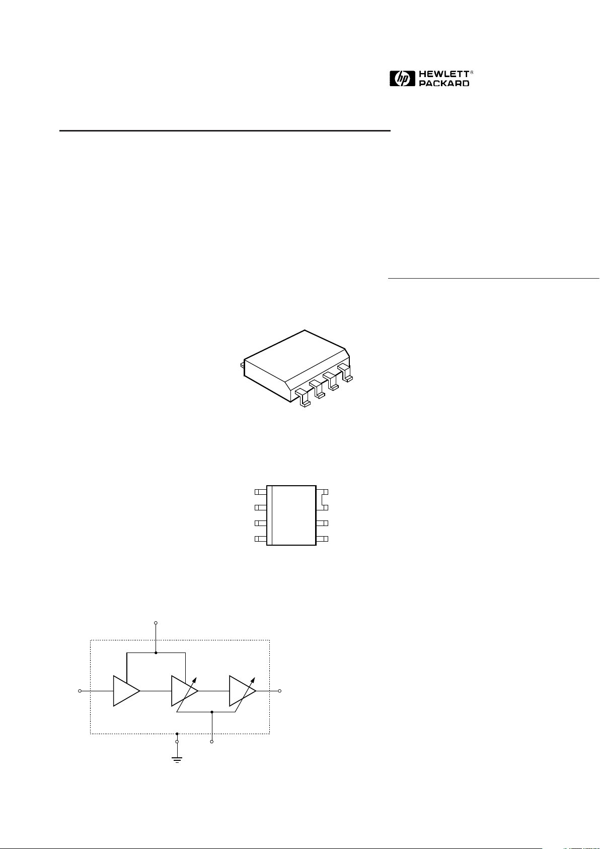
Silicon Bipolar RFIC
900 MHz Driver Amplifier
Technical Data
HPMX-3002
Features
• RFIC Medium Power
Amplifier
• 150-960 MHz Operating
Range
• +22 dBm Typ. P
ldB
, +23 dBm
Typ. P
sat
@ 900 MHz
• 50 dB Typ. Power Control
Range
• 6 V, 160 mA Operation
• S0-8 Surface Mount Package
with Improved Heatsinking
Applications
• Driver Amplifier for GSM
Cellular Handsets
• Driver or Output Stage for
900 MHz ISM Band
Transmitters
• Driver or Output Stage for
Transmitters Operating in
the 150-960 MHz Range
Plastic S0-8 Package
Pin Configuration
Description
Hewlett-Packard’s HPMX-3002 is
a silicon microwave monolithic
integrated circuit driver amplifier
housed in a S0-8 surface mount
plastic package. It operates over
the 150 - 960 MHz frequency
range, and at 900 MHz it produces
+23 dBm of saturated output
power, has 30 dB of small signal
gain and a 50 dB power control
range. The amplifier has a wellmatched input, and an open
collector output which provides
good linearity and efficiency and
is easy to externally match to 50
Ω for optimal power output.
This device is well suited as a
driver amplifier for European
GSM (Global System for Mobile
communications) portable and
mobile telephone systems, or as
the output stage for other low
cost applications such as 900 MHz
ISM band spread-spectrum.
The HPMX-3002 is fabricated with
Hewlett-Packard’s 15 GHz f
t
ISOSAT-II process, which
combines stepper lithography, ion
implantation, self-alignment
techniques, and gold metallization
to produce RFICs with superior
performance, uniformity and
reliability .
Functional Block Diagram
1
2
3
4
8
7
6
5
GROUND AND
THERMAL
CONTACT
V
CC1
GROUND
RF
IN
GROUND AND
THERMAL
CONTACT
RF
OUT
AND V
CC2
POWER CONTROL
(4)
RF
IN
(1, 3, 7, 8)
GROUND
(5)
POWER CONTROL
(6)
RF
OUT
AND V
CC2
(3RD STAGE BIAS,
OPEN COLLECTOR)
(2)
V
CC1
(1ST AND 2ND STAGES)
5965-9661E
6-77
HPMX-3002 Absolute Maximum Ratings
Absolute
Symbol Parameter Units Maximum
[1]
P
diss
Power Dissipation
[2,3]
mW 1400
P
in
Input Power dBm +5
V
CC
[1]
Supply Voltage V 8
V
CC
[2]
Supply Voltage, 3rd Stage V 12
V
cont
Control Voltage V 5
T
j
Junction Temperature °C 150
T
STG
Storage Temperatuere °C -65 to 150
Thermal Resistance
[2]
:
Θjc = 66° C/W
Notes:
1. Operation of this device above any one
of these parameters may cause permanent
damage.
2. T
c
= 25 °C (T
c
is defined to be the
temperature at the ends of pin 7 where it
contacts the circuit board).
3. Derate at 15.2 mW/°C for TC > 58°C.
HPMX-3002 Guaranteed Electrical Parameters, T
C
= 37° C, ZO = 50 Ω
V
CC1
= 4.5 V, V
CC2
= 6 V, PIN = - 6 dBm @ 900 MHz, output matched for maximum power
I
CC1
= 65 mA nom., I
CC2
= 95 mA nom. set by V
cont
(pin 5) = 2.2 V (unless otherwise noted).
Symbol Parameters and Test Conditions Units Min. Typ. Max.
P
out
Output Power PIN = -6 dBm, f = 900 MHz dBm 22 23
PCR Power Control Range f = 900 MHz, dBm 40 50
V
cont
= 0 to 2.2 V
I
CC 1
Driver Stages Current V
CC 1
= 4.5 V mA 65 75
I
CC 2
Output Stage Current V
CC 2
= 6 V mA 95 120
HPMX-3002 Summary Characterization Information, T
C
= 37° C, ZO = 50 Ω
V
CC1
= 4.5 V, V
CC2
= 6 V, Pin = -6 dBm @ 900 MHz, output matched for maximum power
I
CC1
= 65 mA nom., I
CC2
= 95 mA nom. set by V
cont
(pin 5) = 2.2 V (unless otherwise noted).
Symbol Parameters and Test Conditions Units Typ.
P
1dB
Output Power at 1 dB Gain PIN set for P
out
= P 1 dB, dBm 22
Compression f = 900 MHz
G
ss
Small Signal Gain f = 900 MHz, P
in
= -18 dBm dB 32
IP
3
Third Order Intercept Point f1 = 900 MHz, f2 = 901 MHz dBm 29
P
out
per tone = 12 dBm
IP
5
Fifth Order Intercept Point f1 = 900 MHz, f2 = 901 MHz dBm 24
P
out
per tone = 12 dBm
NF Noise Figure dB 9.5
VSWR
in
Input Voltage Standing Wave Ratio - 1.5:1
I
cont
Control Current V
cont
= 0 to 2.2V mA 2.5
6-78
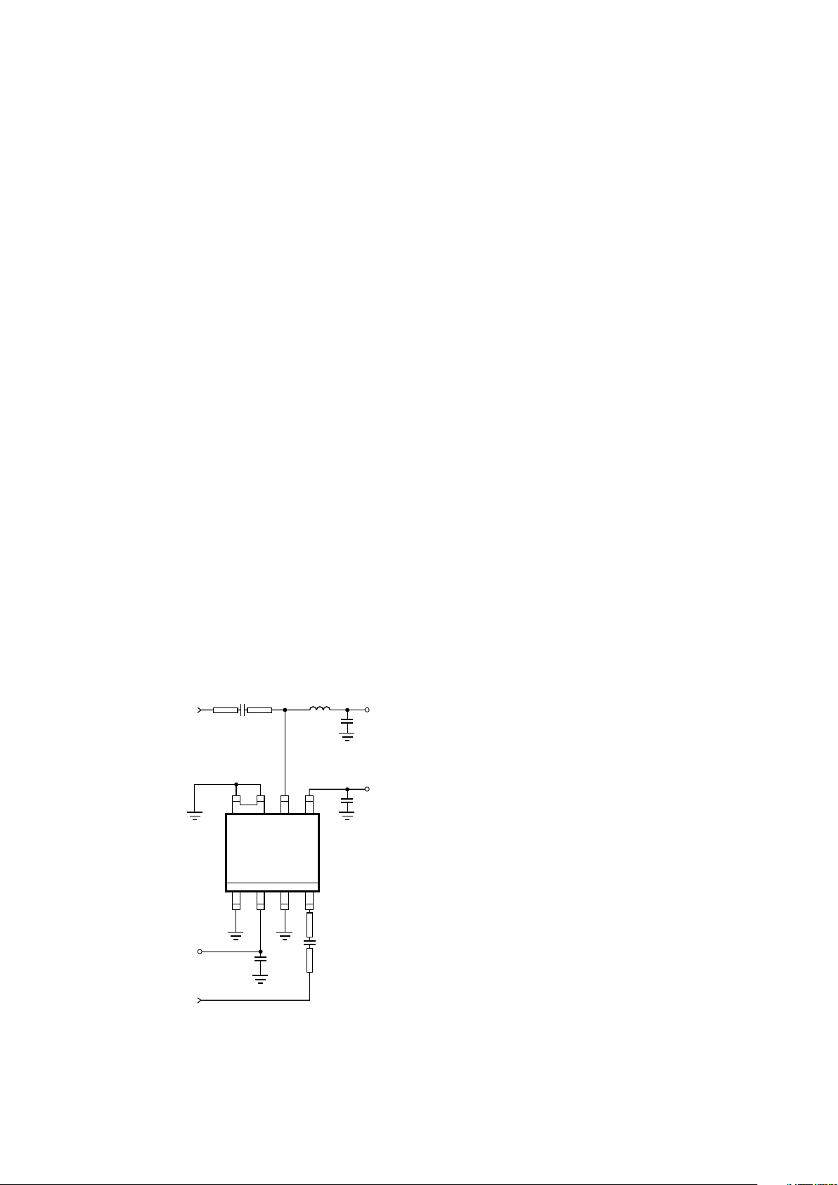
HPMX-3002 Pin
Description
Ground (pins 1,3,7,8):
This RFIC is ground sensitive. A
short path to ground with minimal
parasitics must be provided on all
ground leads to prevent stability
problems. The PC board should
be 0.032" or less in thickness.
Multiple vias should be placed
near the ground leads. Failure to
properly ground this device can
lead to positive return gain and
possible stability problems. We
suggest performing a stability
analysis using the device s
parameters and a description of
the inductance of your ground
path. A recommended board
layout is shown on the final page
of this data sheet. Pins 7 and 8
also provide the primary thermal
path for heatsinking the device.
V
CC1
(pin 2):
This pin provides the DC bias for
the amplifier driver stages, and
has an operating range of 4.5 to 6
V (5 V nominal). It should be
bypassed close to RFIC body
using a 1000 pF capacitor.
RF
in
(pin 4):
The impedance of this RFIC is
well matched to 50 Ω from 100
MHz to 1100 MHz. Normally, no
additional impedance matching is
required. S-parameters are
provided should the designer need
to “fine tune” the input match. Pin
4 must be AC coupled to
generator (1000 pF typ. blocking
capacitor). The nominal drive
level is -6 dBm, and under normal
operating conditions should not
exceed 0 dBm.
Control (pin 5):
Applying a DC voltage to this pin
adjusts the gain of the last 2
stages of the RFIC over a 50 dB
range. Pin 5 has an operational
range of 0 to 2.5 V. The power
control function is designed for
operation in the 800 - 1000 MHz
frequency range, and decreases in
adjustment capability at lower
frequencies – refer to the
performance graphs (figure 3).
RF
out
and V
CC2
(Pin 6):
Pin 6 connects to the open collector of the output stage. A power
match is required at this pin. The
typical match for operation
between 800 and 1000 MHz
consists of a shunt L (8 nH typ.)
and a series C (27 pF typ.), with
the series C also serving as the
blocking capacitor. The s
parameter data should be used to
generate matches for other
frequency bands.
Figure 1. HPMX-3002 Typical 900 MHz Amplifier Use.
27 pF
TRANSMISSION LINES ARE 50 Ω
PIN:
1827364
5
1000 pF
RFIN (50 Ω)
1000 pF
V
CC1
(4 TO 6 V,
65 mA NOM.)
V
CC2
(4 TO 8 V,
95 mA NOM.)
1000 pF
8 nH
RF
OUT
(50 Ω)
OUTPUT POWER
CONTROL VOLTAGE
(2.2 V, 2.5 mA TYP.)
 Loading...