HPMX
2007
YYWW
i 1
i 2
LOmod 3
RF
OUT
4
RF
OUT
5
IF 6
IF 7
ENABLE 8
16 q
15 q
14 mod
13 mod
12 V
CC
11 V
EE
10 LOmix
9 LOmix/M IXOFF
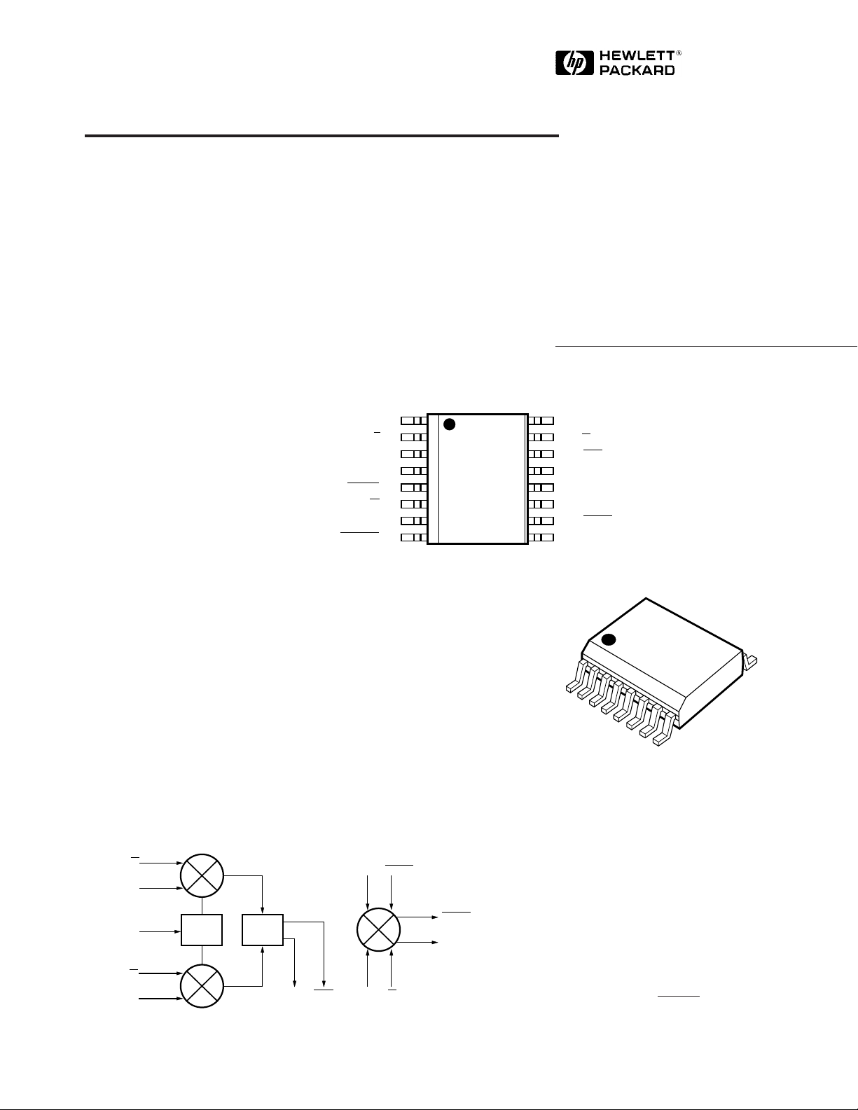
Vector Modulator/Mixer
Technical Data
Package Pin ConfigurationFeatures
• 5 MHz to 4 GHz Overall
Operating Frequency Range
• 40-400 MHz LOmod range
• 2.7 - 5.5 V Operation (3 V,
25 mA)
• Differential High Impedance
i, q Inputs
• On-Chip Linear RC Phase
Shifter
• -23 dBm Modulator S.E.
Output Power into 50 Ω at
150 MHz
• -15 dBm Linear (-11 dBm
Saturated) Mixer Output
Power into 50 Ω at 1900 MHz
• Mixer Can Be Used for
Up/Down Conversion or
Disabled (3 V, 10 mA)
• Standby Mode (<1 µA)
• JEDEC Standard SSOP-16
Surface Mount Package
Functional Block Diagram
i
i
LO
mod
q
q
5965-7239E
φ
Σ
Applications
• NADC, PDC, GSM Handsets
and Base Stations
• PCS Handsets and Base
Stations
• DLMR Handsets
• CDPD Radios
• ISM Band Wireless Links
LO
LO
mix
MOD MOD IF IF
mix
7-74
RF
RF
OUT
OUT
HPMX-2007
Plastic SSOP-16
HPMX
2007
YYWW
General Description
The HPMX-2007 vector
modulator/mixer IC is designed to
meet the needs of cellular and
PCS telephone applications.
The heart of the IC is a vector (or
quadrature) modulator followed
by a Gilbert cell mixer. The
modulator and mixer can be used
together, drawing only 25 mA
from a 3.0 volt supply. The mixer
can be disabled by connecting
either LOmix or LOmix to VCC,

allowing operation of the
modulator alone and reducing
current drain to only 10 mA.
The i and q signal inputs are
balanced to insure high common
mode noise rejection.
The output of the mixer is a
differential pair of open collectors.
One collector can be connected
to VCC and the other matched to
50 Ω using a shunt L, series C
network. Alternatively, the output
can be matched to 50 Ω through a
4:1 balun.
The SSOP-16 package insures that
the IC occupies a minimal amount
of printed circuit board space.
The HPMX-2007 is manufactured
using Hewlett-Packard’s 30 GHz
ISOSAT-II process which
combines stepper lithography,
self alignment, ion implantation
techniques and gold metallization
to produce state-of-the-art RFICs.
HPMX-2007 Absolute Maximum Ratings
Recommended Operating Range of VCC = 2.7 to 5.5 V, TA = -
Parameter Min. Max.
VCC Supply Voltage 8 V
Power Dissipation
RF Input Power +15 dBm
Junction Temperature +150°C
Storage Temperature -65°C +150°C
[2,3]
[1]
40 to +85°C.
400 mW
Thermal Resistance:
θjc = 150°C/W
Notes:
1. Operation of this device in excess of
any of these parameters may cause
permanent damage.
2. T
= 25°C.
case
3. Derate at 7 mW/°C for T
case
> 90°C.
Standard Test Conditions
Unless otherwise stated, all test data was taken on packaged parts under the following conditions:
VCC = +3.0 VDC, Z
LOmod input: 149.67 MHz, 400 mV
= 50 Ω, ambient temperature TA = 25° C
out
, single ended
p-p
LOmix input: 1750.33 MHz, -10 dBm, single ended, 50 Ω
Single sideband tests:
i, q input: 10 kHz, 600 mV
differential with VCC/2 = 1.5 V offset.
p-p
See Figure 25 for test setup schematic diagram.
HPMX-2007 Key Guaranteed Electrical Specifications
Standard test conditions apply unless otherwise noted.
Symbol Parameters and Test Conditions Min. Typ. Max. Units
P
out
I
d
SSB Output Power -17.5 -15 dBm
Unwanted Sideband Output Level in SSB Mode -40 -30 dBc
LOmix + LOmod Leakage Relative to SSB -35 -27 dBc
Output Power
Device Current (ENABLE Open) 25 30 mA
Device Current, Disabled Mode (ENABLE = V
)525µA
CC
[2]
7-75

HPMX-2007 Summary Characterization Information
Standard test conditions apply unless otherwise noted.
Modulator-Only Mode Typ Units
DC Current Drain 10 mA
i, q Input 3 dB Bandwidth >90 MHz
LOmod Input Frequency Range (for Sideband Suppression > 30 dBc) 40-400 MHz
SSB Output Current (Open Collectors). See Figure 26. 2 mA pk-pk diff.
SSB LOmod Suppression @ 150 MHz -35 dBc
DSB 3rd Order IM Products @ 150 MHz -45 dBc
Output Noise Floor -160 dBm/Hz
Modulator + Mixer Performance (Output at 1900 MHz) Typ Units
Total DC Current Drain (Mixer Cannot Be Used Without Also 25 mA
Turning On the Modulator)
Mixer IF Input 3 dB Bandwidth 400 MHz
Differential Output Current (Open Collectors). See Figure 26. 12 mA pk-pk diff.
Linear Output Power. See Figure 25. -15 dBm
IM3 Output Power. See Figure 19. -22 dBc
Output Noise Floor -153 dBm/Hz
LOmix Leakage to RF Output -22 dBc
HPMX-2007 Pin Description Table
No. Mnemonic Description Typical Signal
1 i Balanced modulation input 600 mV pk-pk differential
2i
Z = 75 kΩ || 0.5 pF
3 LOmod Modulator LO input 40-400 MHz, -10 dBm from
Z = 5 kΩ || 0.5 pF 50 Ω source
4 RF Balanced mixer RF output open collectors 5-4000 MHz, 12 mA pk-pk differential,
5RF
Z = current src. || 3 kΩ || 0.7 pF
6 IF Balanced mixer input 40-400 MHz, 350 mV pk-pk diff.
7IF
Z = 5 kΩ || 0.5 pF
8 ENABLE Chip enable input 3 V CMOS logic compatible
9 LOmix/mixoff
Balanced mixer LO input and mixer
enable line
10 LO1
11 V
12 V
EE
CC
Z = 1 kΩ || 0.6 pF
Chip substrate connection 0 V (DC and AC ground)
Power supply connection +2.7 - 5.5 V
13 MOD Balanced modulator RF output 40-400 MHz, 2 mA pk-pk differential
14 MOD
open collectors
Z = current src. || 35 kΩ || 0.7 pF
15 q Balanced modulation input 600 mV pk-pk differential
16 q Z = 75 kΩ || 0.5 pF average value of V
Note: Impedances shown are AC equivalents at each pin, relative to ground. See Figure 26.
average value of VCC/2
with network shown in Figure 25
-10 dBm from 50 Ω source network
shown in Figure 25
with network shown in Figure 25
/2
CC
7-76
 Loading...