

Page 1
o
.(D
s
c
L
o
P
E
R
A
T
ruGAFiä3
s€Rtvt#ffi
MAru
g-F
A
l-
7:'
;s,
;;:''
tt,,,,t,
?i'-"
';i:
'
;
M
U
ITIM
ETE
R
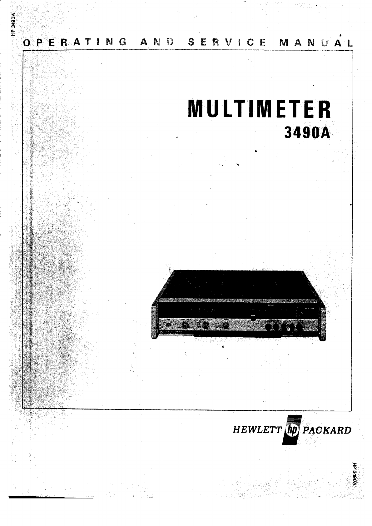
349:04
HEWLETT
PACKARD
T
!-,
ö.,
A
(o.
D=.'
Page 2
HEWLE"WPACKARD
CE
RTI
FI
CATI
tII
O
The Hewlett-Paclnrd
thoroughly
specifications
Paclard
m,mts
tlrc
ertmt allowed
tested,
Com,pany
are traceable
ond. inspected
whm it
further
by the Brneau's
to
WARRA]TTY
All Hewlett-Packard
materials
from
nents
will
repair
the warranty
Packard.
liable
and workrnanship."'This
the date of
listed in
or replace
No
for
consequential
delivery,
the
operating
period
other warranty
Company
was
shipped
certifies
the
U.S.
ATD
products
or, in'the
manual,
products
provided
damages.
which
is
certifins
and
lrom
Natiornl
that
this instrammt
fourd
tlmt
calibration
to meet its
the
factorU.
its
calibration rneo$re-
Bureau
facility.
ASSISTAITCE
warranted
are
warranty
case of
for
the specified
prove
they
expressed
are returned
against defects in
applies
certain
to be defective
or implied. We
pu,blished
The Hewlett-
of
Standards
for
one
major
to Hewlett-
compo-
period.
during
are not
was
to
year
We
Service
for
pair
For
Service
contracts
Hewlett-Packard
on-site.
any
assistance,
Office. Addresses
or customer
products
contact
your
provided
are
assistance
that require maintenance
nearest
agreements
Hewlett-Packard
at
the back
are
of this manual.
available
and re-
Sales
and
Page 3
v
!;:,'
;.t;
:i;
!:..
::::
OPERATING
The main
.:
-:
:
'.
"
Any changes
printing
supplied
supplement,
which apply to
the manual.
factured
will
before
AITD
Manual Part No.
Microfiche Part No. 03490-90064
MODEL
M U tTIM
body of this
made in instruments
be found in
with this
if one exists
your
Backdatinginformation
this
SERYICE
03490-90014
3490A
ETE R
manual
Serial Prefix
manual. Be
instrument
printing
applies to
"Manual
a
for
this manual,
will
MAIIUAI
1211A
manufactured
Changes"
sure . to examine
and record
for
instruments
be found
after
supplement
for
any changes
these
changes
in
Section VIII.
this
this
in
manu-
Copyright Hewlett-Pack
Box
301,
l,oveland,
P.O.
afi
Company | 97 2
Colorado 80537
U.S.A
Printed:
APRIL
1974
Page 4
Model3490A
Table
of
Contents
Section
I.
Section
II.
Section
Iil.
GENERALINFORMATION...
l-1.
l-5.
l-8.
l-10.
INSTALLATION
2-l2-3.
2-5.
2-8.
2-10.
2-14.
2-16.
2-17.
2-19.
2-21.
2-23.
2-25.
2-27.
2-29.
2-30.
2-32.
2-34.
2-36.
242. Sample/Hold
Introduction
Specifications
Options
AccessoriesSupplied
AccessoriesAvailable
l-12.
Instrument
l-14.
Identification
Introduction
Initiallnspection..
Power Requirements
PowerCordsandReceptacles
GroundingRequirements...
Environmental
Installation
BenchUse
RackMounting....
Installationofoptions
Isolated
Option 021
Isolated Remote
(hpllr22{).
Option050andOption060
InterfaceConnections
Data Output
RemoteControlOption
Rear Input
General
Connections
2-38.
24O
246. RepackagingforShipment
OPERATING
3-1.
3-3. InstrumentCapabilities
3-43-6. Output
3-9.
3-ll.
3-13. Front and Rear
3-15. MadmumlnputVoltages
3-17.
3-18. Turn-OnandWarm-Up
3-20.
3-24.
3-26.
3-28.
3-30.
3-32.
InterfaceCableLength
Trigger
GPIBOption030
Option
INSTRUCTIONS.
Introduction
Standardlnstrument
Sample/Hold
Ratio Option
General Operatinglnstructions
Guarding
FloatingMeasurements
Overrange
Overloadlndication
Rangelndication
Functionlndication
....
and Manual
ANDINTERFACE
Requirements
Data OutPut
(-hp
lll2lA)
OPtionO22
OPtion
Purpose
Connections,
UO|O4|
and Remote
Measurements
021
022.....
Interface
Connections,
. .
Control
080 . .
Panel
..
040
Description
...........3-l
.....
Option
Bus
or &15
TABLE OF
......I-1
...1-l
.'-.l-l
-......1-1
...1-l
...1-1
......1-2
.. ... .2-I
. .
..-2-l
....2-l
- . .2-l
.. - .....2-l
.. . - ..2-1
. . .
. - . . . 2-l
. . .
....2-2
-...2-2
-...2-2
....
-...2-2
....
. . . .. .2-2
..
---..2-2
.....
..
...'....2-3
.. .
-. -2-3
. . .24
...'-..24
......2-6
.......2-8
. .. .
. ..
.....2-9
..
--...'.3-l
....'...3-1
Options
. ' . .3-1
.. . .
..
- . .
.
. -...
......3-2
.....3'2
.....
. . . . .
. . . .
........3-3
...-....3-3
........3-3
Page
Page
-2-3
-2:2
.2-8
Page
..3-I
...3-1
.3-l
. .3-l
-3-l
..3-2
-.3-2
- 3-3
CONTENTS
Section
-'-''
':
(cont'd)
III
3-34.
3-36.
3-38.
340. DCVoltageMeasurements
342.
344.
346.
348. AC
3-50.
3-52. Inputlmpedance
3-54. HarmonicDistortion
3-56. Resistance
3-58.
3-60.
3-62-
3-64. External Trigger
3-66. Data Output
3-68.
3-71. Input
3-73.
3-75. Remote Control
3-77. InputSignal Requirements
3-79.
3-81. Remote
3-83.
3-85.
3-81.
3-90.
3-101. Talk
3-103.
3-131. GPIB Operating
3-136. Control
3-139.
3-140. Definition
3-152.
3-156. Guard Connection
3-158. Input
3-160.
3-165.
3-173. Usingthe
3-179. Using
3-182.
3-184.
3-186.
3-188.
3-190.
3-192.
Autoranging
ManualTrigger
Self-TestOperation
DC
Sample
ResponseTime.
Input Resistance
ACVoltageMeasurements
Sample
ResponseTime.
FrequencyRange.
Measurements
InputConnections
Signal Voltage
Ohms
Ohmmeter
ResponseTime.
Output Signals
Sigrals
Data Output
OutputSignals
Programming
Remote Control
Remote Control
General
Sample/Hold
Purpose
I/O(Option030) .
Bus
GPIB
Only
GPIB Control
by
Programmer
(Option
Special S/H
Considerations
Measurements
Signal
Sample/Hold
Requirements
Initiating
Measurement
the
50
Using
Measurements
Ratio
External
InputConnections
RatioDisplaY
RatioMeasurementProcedure
and
Rate
.. . .. .. ... .34
Rate and
.. ........34
. ........3-5
and Current
Sample
(Option
Signals
(No
040
of
a
Track/HoldMode
Acquire/Hold
Hz
Reference
Rate and
(Option
O2l)
and
l,evels
and hvels
Isolation
(Option
of Test
Isolation . .
Interface Bus
Controller) . .
of3490A
Example
Marked Card
Measurements
or 045)
Sample/Hold
Operating
....
in
.....
Limitations
Trigger Signal
.....
Sample/Hold
Hz
or 60
(Option
Voltages
........3-3
...........
........34
. . . . . . . . . . . .34
. . .. .
020)
. .
022) ..
..... ....34
Procedure . . . .34
Function . . .34
........3-7
..
Terms . . . 3-15
Sample/Hold
Mode
Power
080).
.
Page
......3-3
....3-3
3-3
....34
.....34
....34
...34
. . . . 3-5
....3-5
. 3-5
. .
. . .3-5
3-5
. . . .
. . . . .34
.
.. . . . .3-6
..
. .34
. .
......36
. .34
. . . .3-7
. .
. .
. . . 3-8
.. . . .3-8
. . . 3-13
.....-3-14
. . . .3-15
......3-16
......3-16
.
.3-16
..
.....'3-16
-3-17
....
.... ..
Source . 3-21
. 3-18
. .
. .
.3-20
. . .3-21
- - -. ...3-21
.......3-21
......3'21
-3-21
.' - -
iii
Page 5
Table of
Contents
Model 34904
Section
IV.
4-48.
4-50.
4-52.
4-54.
4-56.
4-58.
440.
442.
444.
4-66.
448.
4:70.
4-71.
4-73.
4-75.
4-77.
4-79.
4-81.
442.
444.
4-86.
+88.
4-90.
4-105.
4-107.
4-113.
+l15.
+117.
4-1
+122.
+118.
THEORYOFOPERATION
4-1.
4-3.
4-5.
4-7.
4-9.
4-ll.
4-13.
4-15.
4-17.
4-19.
4:21. InputAttenuator
4-23.
4-25.
4-27.
4-29.
4-31.
4-33.
4-35.
4-37.
4-39.
440.
42. IntegratingAmplifier
4
446.
Introduction
General Theory
Signal Conditioning
ReferenceVoltages
DC
Amplifier
Analog-to-Dgital
Logrc .
Display
Range
and Function
DC
Analog
DC
DC Amplifier
SwitchingCircuits
BootstrapCircuit
Reference
OverloadProtection
Leakage
DC
Integrator
Dual-Slope
44.
x
20 Amplifiet
ZeroDelectAmplifier
ElectronicSwitch
Integrator
AC
Converter
AC
ConverterAmplifier
Rectifier
OhmsConverter....
CunentSource
Ohmmeter Power
OhmmeterReference
InputProtection...
Dsplay
Display
ScanGenerator....
ScanDecoder
PolarityDisplay
Decimals
IngicCircuits
Clock.
DataCounter
Buffers
Timing
Algorithmic
Input
Transfer
OverloadStorage
DC
Switching
ReferenceSupplies
18.
Voltage
RatioMeasurements
(Option080)
Front
Circuits
Amplifier
Voltages
Control
Amplifier
Circuits
Integration
Auto Zero
Attenuators
and Filter
Assembly
Units .
and
Counter
State Machine
Polarity
andZero
Logic .
Measurements
Panel
Switching
.
of
Operation
Circuits . . .
Converter
Control
..
Gain .
Auto Zero
-..
..
Supply
(Figure
Annunciators
....
Storage
.
7-27).......44
Detect
....
TABLE
........4-I
...4-l
. . .4-l
. . . .
...4-l
......
.
. .
. .. . . 4-l
......4-l
......4:2
. . . -
. . . 4-2
.. - .4-2
........4-z
. .....
... .....4-3
....4-3
....4-3
. .
........43
.....43
. .
. . .4-3
.
.. .
.. .,..4-s
.......4-5
. . .M
......M
....M
. . -
...
.
. .44
...44
........44
. . .
...*7
......4-7
.
. . .4-7
.......+g
..+9.
......4-g
........+g
.......4-8
.....4-8
. . . . . . .
....4-8
......43
.......+9
......+9
.
.. . .
. . . .
. . .
.
.. . .
.
. . .
...+13
. . +13
...+13
.......
....+14
.
... . . .4-15
0F C0NTENTS
Page
. 4-l
.4-l
.+3
.4-3
.4-s
.44
+7
,"
. 4-B
+9
+ll
4_12
4-12
+13
(Gont'd)
Section IV
4-130. PowerSupplies
4-132.
4-134.
+137.
4-139.
+141.
4-143.
4-145.
+147.
4-149.
4-150.
4-152.
4-154.
4-158.
+160.
4-162.
4-164.
+166. Isolation
4-168.
+170.
4-172.
4-174.
4-176.
+178.
4-180.
4-182.
4-184.
+186.
4-188.
.
+19O.
4-192.
4:194.
4-196.
+198.
4-201.
4-204.
4-212.
+214.
+216.
4-218.
4-221.
4-228.
Section
V.
MAINTENANCE
5-1. Introduction
5-3.
5-5. TestRecord
5-7. PerformanceTests.
5-9. DCVoltmeterAccuracyTest..
5-l l.
5-15.
5-16.
(cont'd)
...
Self-TestFunction
LogicTest,No.
lOVRangeZero,TestNo.
TurnoverError,
f
ReferenceCheck,TestNo.
0.1 VRangeZero,TestNo.
x.0l
Atten., x 100
TestNo.6....
Ohms
Reference,TestNo.
BCD
Remote
(FigureT-31)
Outguard Power
Isolated
Sample/HoldTriggerCircuits
Data
DataMultiplexers
DataOutputSequential
Data
ShiftRegisters
DataFlag
PrinterHold.
Remote
Circuitlsolation
RemoteEnable
OutguardMultiplexer
Remote
Program
Data
Shift
Local/RemoteMultiplexers
Local/RemoteFlip-Flop
Data Flag
General Purpose
I/O
GPIBSystem
Basic
GPIB
Sample/Hold
Track/Hold
Acquire/HoldMode
Sample/HoldMeasurement
Sequence
Sample/HoldAnalogCircuits
Sample/Hold
RecommendedTestEquipment.
AC Voltmeter
OhmmeterAccuracyTests..
PreferredMethod
Trigger
Output
Clock
Control
Sequential
Clock
Registers
(Option
Theory
System
...
I
.
TestNo.
Expand
Supply
and Hold
Option
Assembly
Flag
Option 040 or
Mode .
Accuracy
021
..
....
Option 022 .
Logrc
.
Interface
030) .
of
GPIB I/O
Operation
Logic
Circuits . .
Tests
Gain,
Option
..
Logic .....
Bus
.
.
....4-16
2
. .....
3
. .......
4 .....
5
. .....
7 .
......4-17
020
.....4-t7
- . . .4-l,l
.
..
.......4-18
.......4-19
......+19
.. .
. .. .+19
-...+19
...-.+19
......+19
.
...
.....4-20
. ......4-20
....+2O
.. ..
......4-20
Circuits
. .
045 . . . .
......4-22
...
...4-23
. . . . . +25
... . s]r
.....5-l
..
...
.....5-l
......5-l
.... -5-2
......5-2
page
...4-15
..+16
+17
4-17
4-17
4-17
..4-17
zt-18
. .
.
.. . 4-18
. .
.4-18
4-18
.
. +lg
. .4-18
...+19
. - 4-19
-.+19
. .4-20
.
. .4-20
. . .4-20
. . +21
. .4-21
.4-22
. .4-22
..+22
Pase
.. .
5-l
...5-l
. . .
5-l
ir-
Page 6
Model3490A
Table
of
Contents
(cont'd)
Section
Section
VI.
V
5-18.
5-2O-D0Common-ModeRejectionTest ......5-2
5-22.
5-24-
5-26.
5-28.
5-30. Sampli/Hold
5-32. Sample/Hold DC Measurement
5-34.
5-36. RatioPerformance(Option080)..
5-38. DC/DC Ratio
541. AClDCRatioAccuracyTest
543-
545. GPIB
547.
549.
5-51.
5-53. PowerSupplyAdjustment
5-55.
5-57.
5-59.
561.
563.
544.
5-65.
5-66.
5-69.Sample/HoldAdjustments.
5-71.
5-73.
5-75.
5-77.
5-79.
REPLACEABLEPARTS
6-1.
6-1
6-6.
6-8.
Ätemate
A9Common-ModeRejectionTest
AC Normal-Mode
DcVoltmeterlnput
Resistance
AcVoltmeterlnput
ImpedanceTest.
(Option04OlO45)
AccuracyTest..
Sample/Hold Response
ExternalReferenceinput
ResistanceTest..
General
Test Procedure
Model
AdjustmentProcedures...
DCZeroAdjustments..
ReferenceAdjustments...
DC
Amplifier
ACCorrverterAdjustments
lVRangeAdjüstments
l0VRangeAdjustments
100
OhmmeterAdjustments..
Offset
Offset
Dielectric
Response
Ratio
Introduction
Orderinglnformation
Non-Listedparts
ProprietaryParts.
Method
Test
Performance
Accuracy
Operational
Test Procedure
Using
98204
Calcrilator
Adjustments
V
Range
Aäjustments
Gain
Adjustment
Adjustment
Absorption
Adjustment
Reference
Adjustments
Rejection
..
Test
Tests
(Option
Check
.
.-.
.
Adjustment
......
.
rABLE
Test
..
030)
.
......5-14
.......5-15
......s-15
......5-16
. ..
........6_l
OF
CONTENTS
Page
. .
... .5-2
......54
......54
....
.54
.....S-5
.....5-5
......54
...
..5-6
......5-7 711.
.....5-g
.....5-8
..
.5-8
.
. .
5-l I
. . .
. .
l
5-l
.....5-14
.....S-15
.....5-15 !'t7'
.....5-16
.
. .
.
5-16
.....5-16
.. .5-16
. . .5-17
.
.. .5-17
..
. .
......6-I
.....6-l
.....6-l
S-iA
.5-lg
page
...6:l
t^'
r.
(Cont,d)
Section
VII.
SCCtiON
VlI.
TROUBLESHOOTING
CIRCUITDIAGRAMS
7-1.
7-3.
7'5.
7-77--9.
7-13.
7-15-
7-177-22.
7-25.
7-27.
737'
!19
t4z'
- ,6 _
t4ö-
7-50.
t-)2'
!-)5'
1-t?'sample/HoldSJrvicing
!-bu'
743'
!t2
t4'1.
749-
7'73.
7-75.
7'77.
BACKDATING
g_1.
g_3.
g-5. partsNotUsted.
Introduction
Preliminary
TroubleshootingTrees
Access
PowerSupplyChecks
DCAnalogCircuits
,{2
DCAmplifierChecks
DC
ReplacementofQCR3Ol
A-to-D
IntegratorTroubleshooting
OhmsConverterTroubleshootlng.....74
DisplayTroubleshooting
LogicTroubleshooting
Suggestions
Data
(Option
Remote
(OptionO22)
GPIBTroubleshooting
(Option030)
GeneralChecks
ExternalTriggeiCircuitCheck.
AccesstoSample/HoldCircuits
Operating
Sample/HoldAssembliesRemoved..T6
Sample/HoldTroubleshootingTrees...T4
Ratio
External
Checks
Reference
SchematicNores.
Logic
Introduction
Change
AND
Troubleshooting
for
Servicing
Assembly
Amplifier
Conversion
Output
Control
Troubleshooting
Gate
....
Sequence
Exchange
Switching
Circuit
..
. . .
Troubleshooting
O2l) .
Troubleshooting
.
.
the
3490A
Reference
.
Polarity
Symbols
Amplifier
Logic
.......7-l
...
...
........7-l
........7-l
.......7-2
Circuits
Checks
............7-s
with
Checks
.
.
..........74
. . .
.....7-5
.....'l-5
......7-s
.....74
........74
.....74
. . ..
.....7_g
.....g_l
........
........g_l
page
...7-l
. . .7-l
..
. .7-l
....7-2
.
. . .
.7-2
. . .
.7-3
....7-3
..
. .7-3
..
.7-5
. .7-5
. . ..7-8
.
. .
.7A
. . .
. 7-8
.
. .
.7-g
PAgE
... .8_l
g_l
APPENDICES
A.
Code
B.
Sales
List
of Manufacturers
and
Service
Offices
Page 7
Table of Contents
Model 34904
LIST
OF
Figure
2-1 . Line Voltage Selection . . .2-l
PowerCordConfigurations .... .......2-l
2-2.
2-3. Model3490ADimensions ......2-2
24. Installation of
and
2-5.
Data OutputConnections, Option 021 ........24
2-6. Remote
2-7. RearlnputConnectorandCable .......2-6
2-8. Interface Bus Cables
2-9. General
2-10. Tigger Connections, GPIB Option 030 . . .. . .
2-l I . Trigger Connections
3-1. Front and
3-2. Connecting the Guard .
3-3.
OhmmeterlnputConnections . ........3-5
34. External Trigger
3-5. Option
3-6. Remote Program
3-7 . Position of Jumper
Mother
3-8. Timing Diagram,
3-9.
Timing Diagram, 3490A
3-10.
Example ofMarked CardProgramming
3-1 l. Typical Response to
InputVoltage....
3-12.
Di$tizingaRamp
3-13. Using Delayed-Sweep
RampLinearityMeasurements
3-14. Filter
3-l 5.
3-16.
4-1
. Dual-SlopeIntegration
4-2. BasicDiagramandOperation.....
4-3.
44.
4-5.
4-6.
4-1.
4-8. Block
4-9. TypicalStateMachineBlockDiagram
4-10. Block Diagram,
4-l l. Block
4-12. Block Diagram,
4-13.
4-14.
4-15. Input Bias
4-16. ReferencePolarityLogic.
4-17.
418. DataOutputTimingDiagram(Option02l)
4-19. Remote
4-20. T1'pical
4-31. SampleiHold
-1-ll.
Output Measurement
Measurement
RatiolnputConnections.
SimplifiedDiagram,DCAmplifier
Measurement
Simplified Diagram,
Simplified Diagram,
SimplifiedDiagram,OhmsConverter..........4-8
Diagram,
ASMFlowChart.
Diagram,
Simplified Diagram, Reference
and Ratio
Simplified Diagram, External
Reference
PowerSupplyBlockDiagram
(Option
\\'aveforms
Track'Hold\{ode.
Isolated
Remote
Input
Connections, Option
Purpose Interface Bus
Rear
Printout .
021
Board
of a Step
Sequence
Circuits . . .4-13
Circuits
Compensation
Control
022)
Bus
System
Circuir Position .
Illustrating 7-21.
BCD
Output
Options
Connections. . . . .2-J
S/H Option
Panel
Sequence
Sequence
Assemblv A31
3490A
Clock and
Main
Main
Qualifier
Timing Diagram 7-18.
. .....4-19 7-19. Reference Desigrations
(Option
(Option
Wires on Outguard
Addressed
Addressed
a
Step
Oscilloscope
Input
Integrator Circuits . . . . - . . . 4-6
AC Converter
Counters . . .
Logic
Circuits . . . .4-11
Logic
Multiplexer
. .
...
.
. .. . .. .2-3
022 ...
045 . . . -
020) ...
022) . . . . . .3-7
to
Listen . . 3-l I
to Talk
. . . . . .. 3-15
in
. . ...3-20
.. . ... -
. . . . . . . . . .
Page
. .
. . 2-5
. . . .2-6
. .2-8
. . . . . .
. . . . 3-0
. .3-2
. .. . 3-5
. . .3-6
. . . .3-12
..3-18
.....3-19
. . . .3-2O
. . . 3-21
.....3-21
...4-1
.....1"2
......4-3
.44
. .4-7
.4-9
...4-g
...4-10
. .4-12
.
.
4-14
. . .
.4-15
.....4-15
.....4-16
...4-18
. . . .4-20
.4-22 and Switching
..+22
ILLUSTBATIONS
Figure
4-23.
Waveforms
Acquire/HoldMode.
4-24.
Simplified
Operationof
4-25.
Simplified Diagram
4-26.
Aebctric
4-27.
Sample/Hole
4-28. Block
andTriggerCircuits
4-29.
Sample/Hold
4-30.
Sample/HoldMeasurement
2-8
3-8
4-31.
Sample/Hold
Measurement
5-1.
AC Voltmeter
AccuracyTest..
5-2. DCCommon-Mode
5-3. AC
54.
5-5.
5-6.
5-7.
5-8. External
5-9.
5-10.
5-ll.
6-1. ChassisParts
G2. BindingPost
6-3.
7-1.
7-2.
.:7-3. Sample/HoldAssembly
14.
iL'
l-5.
j
4. AC Conveiter
7-7 . Ohms Converter Troubleshooting
7-9. DisplayTroubleshootingTree
j-9.
7-tO. I_ofibClockTroubleshooti"ngTree.......l-2317-24
7-l l. Data
7-12. Remote Troubleshooting
7-13.
7-14.
7-1
7-16. RatioTroubleshootingTree
7-17. Locationof Assemblies
7-20. Schematic
Common-Mode
ACNormal-Mode
DCVoltmeterlnput
ACVoltmeter Input Impedance Test . ... . .....
Sample/Hold Response Test .
ResistanceTest.. ....5-9
Location
Standard3490A
Location of
Location of Ratio Adjustments
SwitchAssembly
Switching
SwitchingOutputsofAlU4Ol
deneralTroubleshootingTree
DC Ana1os Troubleshootins
Loeic Test Troubleshooting
Output
option}2l
option
GPIB
Option 030
Sample/Hold
Tree . .
5.
Sample/Hold
Tree ..
3490A Block
Schematic
Tr,roDetectCircuits,Al ...
Illustrating
Diagram
Absorption
Diagram
Reference
of
Inputs to A2U2 .
022
I/O
Troubleshooting
Diagram,
Diagrant,
and
S/HCircuit
of
Logic Block Diagram .. .
of
S/H Timing
Trigger Timing . . .4-26
Simplified Diagram
Sequence
High Frequency
RejectionTest
Rejection Test . .
RejectionTest .. ..... 5-5
Input
Adjustments,
Sample/HoldAdjustments
.
Assembly
Troubleshooling Tree
Troubleshooting
..
.
.
. .
General Troubleshooting
Troubleshooting
Logic
Diagram
DC Amplifier
Circuits,
Integrator and
A..
Circuit
S/H
Compensation .
Sequence
Resistance Test ..
....
Tree .]-1317-14
Tree
Tree,
Tree,
...
.. .....7-38
Al, A2
..
B . . . . .. ..
. . . . . -
..
and
....7-ll17-12
. . . . .
Tree . . .7-17
....|.-1917-20
Tree
Page
......4-22
....4-23
.4-24
4-25
. .
....
.......4-26
..
. . . . .. .
..
.......5-18
......G31
........1-3
........7-7
.
..1-2517-26
. .i-2717-28
.
...74117-42
4-25
. . .
-...+28
....+29
.....5-2
.....5-3
. .
.54
. 5-5
5-6
-
. .5-7
....5-14
.....5-17
..6-30
...6-31
.
. .7-3
..
i,-1511-16
17-18
.7-21
17-22
.7-2917-30
.1-31
17-32
.1-3317-34
....7-35
....7-36
. .7-37
.7-391740
'.;
Page 8
Model3490A
Figure
7-22.
Schematic
Ratio
Circuits,
7-24.
Schematic
7-23.
Schematic
andCounters,Al
7-25.
Schematic
7-26.
7-?7. l+e;atic
7-28.
222. l*"
7-30.
7-3I.
7-32.
7-33.
Logic,Al
Schematic
41,
A8
Schematic
Range,
atic
Schematic
Schematic
- _Circuits,
khematic
Option
^ .
Schematic
Option
Diagram,
Diagram,
022,
Diagram,
Diagram,
Diagram,
Diagram,
Diagram,
Diagram,
Diagram,
and
Dagram,
Diagram,
Diagram,
Ag,
021,
Reference
Al,
Al3
Main
Clock
..
DC
.....:.
SampleRate
Switchins
power
?ror"r,
Function.
AC
Converter,
Ohms
External
A2),
A2g,
Data
A9,
A10,
Remote
AII,
AI2,
and
Logic,
Al
Suppli€s,
o,
:.
Switches,
e.S--.
Converi"r,
Trissei'
A37:.
Output
Al5:
Ali
tnpui
.
.
-'
LIST
0F
7431:144
.
.
. .
.745;1746
...7_47174g
' -
-
.
. .
.
äl',i_]l
AS
.7_5517_56
.
.7_5717-Sg
--'
X
.7_5917_60
j_6117_62
.
'
.
'
.
.7-6317_64
.7_651746
tLLUSTRAT|0NS
Page
7-3
7-38.
7-39.
740.
8-1
8-2.
(Cont,d)
Figure
7-i+.
schematic
7-35.
7-36.
.
AnalosCircuits,
Schematiö
LogicCircuit:,12S...
Block
I/O
7.
schem.li;;i;;;;;
and
Schematic
Assemblies.
Schematic
and
Schematic
Mother
Component
l2ltA0[55and.Lowr;
Schematic
Seriat
Diagram,
Diagram,
Dagram,
Circuits
ROM
ROM
No.
.
Assy,s,
Diagram,
A30,A35
Diagram,
Assemblies,
Diagram,
Board,
Location,
Diugru.,
r2lr/r}fiss
sample/Hold
A27'
Sample/Hold
3490A
GPIB
ii*,.
A34,
GpIB
Outguard
A32,
OutluarJ'
fil
.:
41
1,
Al
I
Assembly.
.......
.
..
p;;;;;''
A36
:.
Isolation
Serial
anJi;;er
.-.-.
-.
Du;;
A33
No.
.......
Table
ofContents
.7_671j_6g
...7_6917_70
-7
-
.
.
7
.
. .
.7_7317_74
.
...
.
.7_7517_76
7_7717_78
.
.7-7glt_80
...
......
.
1
.
t
Page
-7
i
2
8_3
84
Table
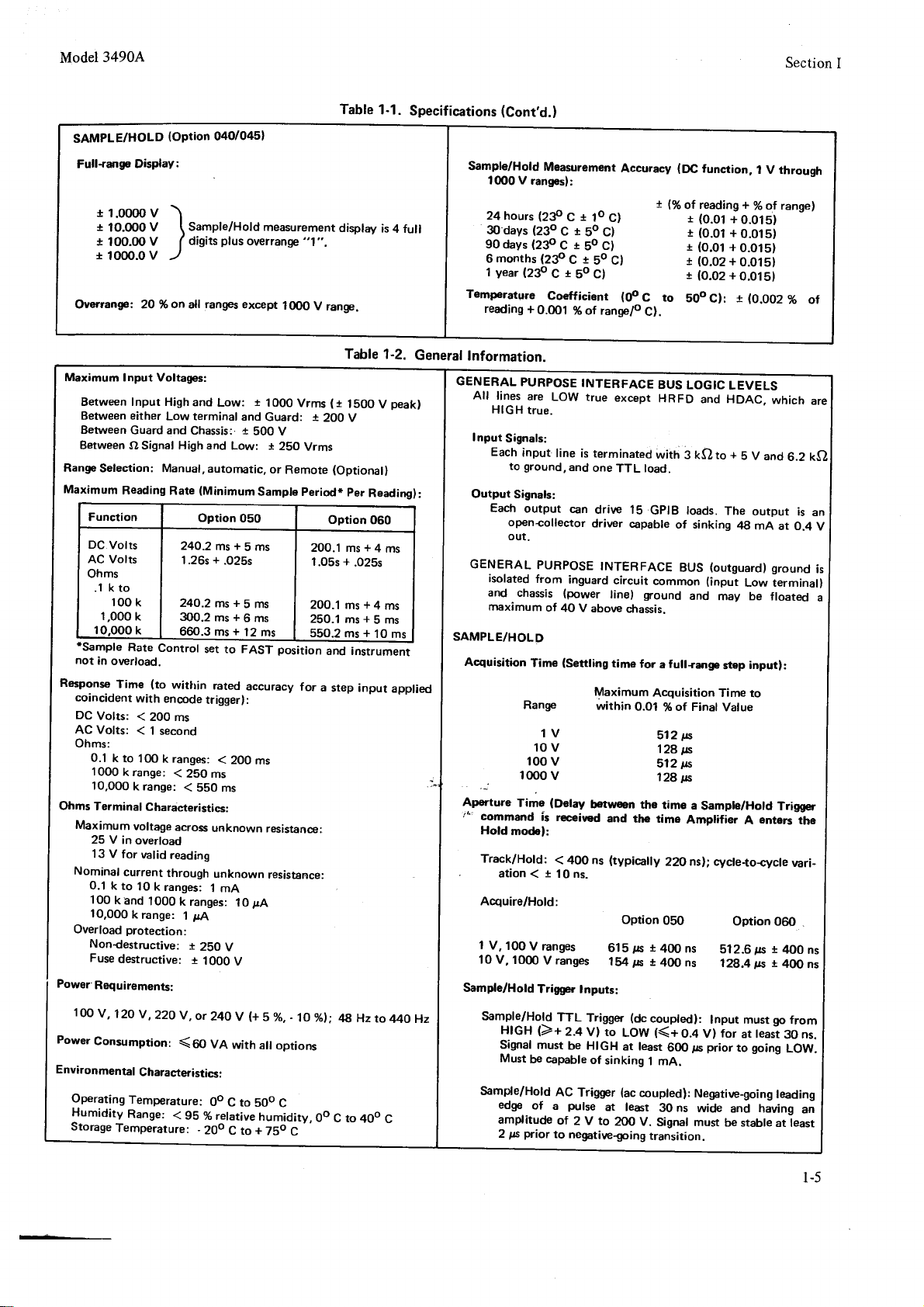
1-1.
Specifications
t-2.
c.n.turrnior*;!;;
|
Option
?
General
?-?
MaximumVoltages
l-1
Sample
1-?.
3-3.
Dstortion
ohil"a;;a;;;;i
11
cfln
2-:
3-6.
Address
3-7.
Programü;..
3-8.
Abti,ty;iöör6l"rä,oic,iirl'
3-9.
Initiating
_.
3-10.
Maximum
^ fiTr
3-1
1.
Ratio
+1.
AC
+2.
Porariry;R;,t"ü'ä;;.;;;,
+3.
Analog
4.
ecquiie/HoioD;i;;...
050
purpose
Rate
Signal
Codes
a
Ramp
byExternalTriggering
for
Polari
AdiG;;üffi'"
Tests
......
and
QRtion
Interface
andResponr.
Error
Mnemonics
. ,
or
Sine
-S/H
Acquisiiön
ty
Wave
Measurements
Full_Range
Disolav"
1Sät
.
.
_
...
OAO
Step
:...
pari
Ctran;;,
Brrä;;;täs
iirnr..
::
:
.
:..
......'........3_7
""""3-9
.
tin
gj
Iäput
........
TIST
Page
.
.
. .
.
.2_3
.....2_7
.....3:2
.......34
:.il
.-3-10
.....3_17
.
.
. .3_tg
"'3-21
.....
frz
"'4-16
4-22
OF
TABTES
5-5.
s6.
5-7.
5-8.
s-e.
5-10.
Gl.
-,^..
7-1.._.
T2
7-3.
71
T:
74.
7-7.
8-1.
Table
Gain
Delay
!-5.
5-1.
Recommendear.rt
5-2.
DCVoltmeterAccuracy
5-3.
ACVoltmeterAccuracy
54.
Ohmmeter
Alternate
sample/HoldDCeccuracyäL;":
DC/DCRatioAccura.v
AC/DCRatioAccura"yf.ri
powerSupplvvoltü;;
Ohmmeter'Adjustment
Replaceabtepärts..
power
CurrentLimitValues
PowerSupplyJlTp"rwires
AC
Reed
component
Data
Output
Alphabetical
Atphabetical
I/OMnem.oni.,
ManualBackdatinlih*;;;
Relationship
Accuracy
Ohmmeter
Supply
Voltages
Retay
Chäcks
Spacing
.irouUierhooti"g
J,istins
Listini;itrö;ä;ö'
...
nq'uip.;;;
Accuracy
färi-.
:1.'..
.
.
......:...::.....
and
.-.
"f
34tö;
:
.
.
.
. .
.
.
.
.
:-.'..
::.............
...................
Test
.
.........
..
:...
:.............
-...
.......
. .
.
.
. .
.
:
:
..
..
np,
.....-.'_
.........
. .
..
.....
ü;rmonir,
....7_7117_72
.
.....s_6
.....
....
.
.
..
..
.....6_2
......7_1
...7_2
.
.
.
. .
.
...
.
.
....8-l
,^X
.
.
.
5_0
5_l
5_3
.
. .
5_3
.
5_7
5_8
s_ls
.5_16
.
.74
.
.74
.7_to
vll
Page 9
Model
34904
sEcTt0N I
GENERAT INFORMATION
Section
I
lNTBoDucTl0N.
1.1.
l-2.
resistance
voltage,
tion.
l2O%
ranges.
Range
on
output,
ments,
1-3.
instructions
Model
procedures
Procedures
to its
the
tion
14. This
mance specifications for the Model 3490A
available options. It
with the
are available.Instrument
mation is
1-5.
l-6. Table
critical
Table
operating
l-7.
turing,
Bureau
sheet
change
ing
r-8.
l-9.
usefulness
and
capable
is
It
range
of
Polarity
selection
functions.
all
remote
ratio
and
manual
This
as well as maintenance
34904 Multimeter.
for
are also included
performarice
theory
of operation, and troubleshooting
provided
are
section
Model
also included.
SPECTFtCATI0NS.
l-l
specifications
l-2
contains
characteristics
Any
change
design,
of
Standards
included
specifications
sheet
with this
supersede
0PT|0NS.
The
following
of the
measurements
of overrange measurements
on all except the 1000V
selection and
is
manual or automatic
Options are available
programming,
measurements.
contains installation
Instrument
verifying
for use
3490A
is
in
or traceability
of rhe
Model
proper
for adjusting the instrument
specifications.
in
maintaining
the manual
of
lists
also
and
and manual
a complete list
that
are controlled
general
information
the
of
the
specifications
will
be listed
manual.
previous
all
3490A.
options
3490A:
are
3490A Multimeter
Model
The
makes
with 5-digit
display are
to
sample-and-hold
information
specifications
operation
Schematic
the instrument.
contains the
the accessories supplied
additional
Model
to
The manual
available to
accessories that
identification infor-
of the
that
3490A.
due to
the
on
a manual change
information
voltage,
ac
ac and
automatic.
over all ranges
provide
and
are
and lists the
Model 3490A
by tolerances.
describes the
U.S. National
and manual
extend
dc
resolu-
up to
dc
data
measure-
operating
the
for
and
included.
diagrams,
informa-
perfor-
manufac-
concern-
the
Option 040 or 045:
Option 050: 34904
power
source
Option 060:
Option 080:
I-Ill. ACCESSORIES
l-ll. The
Model 3490A
Supplied
Rack
PC
Supplied
Rear input
36-pin
5Gpin
Remote Jumper
PC
Supplied
with
Mount
Extender
with
connector
(mates
connector
(mates
Extender
l4-pin
connector
(mates
Remote
Rear input
PC Extender (2
Supplied
S/H Analog
.-'
S/H Logic
PC Extender (2
Supplied with
S/H Analog
S/H Logic
PC Extender
l4-pin
connector
(mates
Supplied
Ratio
Jumper
PC
Extender
3490A
power
Ratio
following
and its
accessories
option
all instruments:
Kit
(2
x l8)
Option 020:
cable
with Remote
with Data
with
Output connector,
Assembly,
(2x22)
Option
with Trigger
Jumper
Assembly,
cable
x 22)
with
Option
Jumper
Jumper
Assembly,
Assembly,
x l0)
Option
Jumper
Jumper
with
with
Assembly,
(2
x l0)
Trigger
Option
Assembly,
Assembly,
(2
x l0)
source
SUPPLIED.
connector,
030:
connector, Jl l)
040:
045:
connector, Jl l)
080:
Sample-and-Hold
designed
desigred
for operation
for operation
are
shown.
as
J7)
A.4
supplied
J6)
44
A24
A25
A24
A25
A26
on
50
Hz
on
60 Hz
with the
03490-84401
5060-s983
o349Mt612
l2sl{084
-0086
I
2s I
03490-66504
5060{630
12514142
0349U66504
0349041612
5060{630
0349046524
03490-66525
50606032
0349U66524
0349046525
50606032
12514142
0349046526
5060-6032
Option
Option
Option
Option
020:
BCD/Remote
021:
Isolated
022:
Isolated
(Options
Option
030:
General
(GPrB)
Expand
Data
Output
Remote
021
and 022
020)
Purpose
(BCD)
Control
require
Interface
Bus I/O
1.12.
ACCESSORIES
l-13.
Several
Model 3490A.
Option
panel
symptoms
accessory provides
705,
accessories
A
service
will
demonstrate
to isolate
AVAITABLE.
are available
video tape, Product
use
failures.
a set
of IC reference
for use
No.
of self-test
The
-hp
boards with
with the
90030C
and front
111261^
1-t
Page 10
Section I
Model
3490A
most
of the 3490A logic
lO529A
Logic
without
-hpcontains
such
Three
030. These
A
available
face
No.
or
for
numbers
Logic
Comparator. Using these
Comparator, a faulty
removing it from the circuit.
11127A, is
the most
integrated circuits,
as
interface
GPIB Repair
Bus I/O circuits.
562A-16C,
50554, Printers. Field
units
cables are available
cables
l063lA Interface
10631B Interface
10631C
for troubleshooting
for use with
with Option
Ill2lA and I I l22A
IC's for
IC can
be isolated
available for
critical components
identical
are
Interface
-hp-
Kit,
Also
installable
O2O are
the 3490A.
transistors
except
cable,3 ft.
cable,6
cable,
Part No.
the
General
available is
Option
Options
available by
respectively.
use
with the
boards with
in seconds
A spare
for the
for length.
12 ft.
0349G80009,
021 and *rp
parts
of
the 3490A
and
reed relays.
GPIB Option
ft.
Purpose
a cable. Product
O2l and,O22
accessory
This
lnter-
50508
-hp
the
set,
set
1.14.
INSTBUMENT AND
MANUAL
IDENTIFICA-
TION.
Instrument
5.
l-1
located on
two-section
prefix
designating the
manufactured.
J
l-16. This
numbers
been made in the instrument
is
printed,
the
these changes
Section
serial
Part
the manual are
and a
=
Japan;U
indicated
a
manual
VIII
numbers lower
numbers
manual
"Manual
identification
the
rear panel.
serial number consisting
five-digit suffix
country in
=
(A
=
United Kingdom.)
will define these
your
in
adapts
for the manual
also
U.S.A.;
applies to instruments
on the title page.
Changes" supplement
manual. Backdating information
the
than
that shown on the
shown
on the
by serial number
Hewlett-Packard
separated
the instrument
which
G = West
since this
changes. Be sure
manual to instruments
the
and
title
of a four-digit
by a
Germany;
with the
If
changes
manual
supplied
to
title
microfiche
page.
uses
letter
serial
have
with
record
with
page.
copy
is
a
was
was
in
of
l-
Page 11
Model 3490A
VOLTAGE
DC
Full-Rangp
Overrange: 2O % onall ranges
Aeuracy:
24 hours
{23oc
30 days
(23oc1soc)
90 days
(23oc
6 months
{23ocisocf
year
1
{23oc!soc)
Temperaturo
O.1 V
'
1V
Voltage
reading.
Effectlve
either
AC:
DC:
AC Normal{Vlode
Option
Option
Input
O.1,V
100
AC
VOLTAGE
Full-Range
Overrange:
ttTlgnt
10'
Accuracy:
lnput
Guard
24
hours
(230
C r
3)
days
(230Cr50c)
90
days
(230C150C)
6 months
(23()C15()Cl
ye€r
l
(230c+5()Cl
I
Frequencies
l0
Display:
t
l%
!
loc)
r5()c,
Coefficient
Range: t
range)/o
+
Option
Option
!O.l%
to.1
Resistance:
V
nnximum
10
C
through
0.OO03
Coefficient
Common{lode
loadf:
O5O
50H2t0.1
060
6OHzt0.1
)
140dB
05O
060
%
through
and
lü)0
Display:
2O%on
Rango:
x
l%ot reading
levels
above
must
be
20
Hz
0.32+0.05
cl
0.35+0.05
0.35+o.os
0.4
0.45+0.07
ranges
greater
only.
V
% of
(5O
(60
10
Volt-Hertz
connected
.
:1P9P.Y
i
I;IBBBB V
reading +
of
.1 V
(0.005
t
(0.01
I
(0.01
!
(0.013
r
(o.015
t
(0o
(0.00,l
1OOOV
rangelp
I 000
{
(SO
Hz
%
(@
Hz
%
Rejection
power
Hz
power
Hz
V
ranges
V ranges:
I.OOOOO
10.0000
100.000
1000.00
all ranges
20
Hz
to
1 % of
+0.06
than
except
1000
To
of rangel
Range
+
0.001
)
+
0.005)
+
0.005)
+
0.0051
+
0.0051
C to
50o
Cl:
%
of
reading
Ranges:
C
V range)
Rejoction
:
t
power
power
frequencyf:
frequency):
(<
70%
10
MO
V
v
v
v
except
250
kHz
product
% of
range)
range
to
Low
50
Hz
:
Add
(with
frequency):
frequency):
R.H.):
I
O.1S
IOOO
(Guard
lO.oo+0.025 |
+0.025
lo.r
+o.o2s
lo.t
o.r
+0.03
|
o.tz+o.o3s
|
lO0
kHz
Table
r
10O.oOo
.
rooo.öö
1V-f00{,VRangas
r(O.OO1
0.04
%
V
100
v
v
V
range
(0.004
(0.008
+
(0.01
+
(0.013
+
(o.015
+
+
0.0007
% of
ppm/vott
1
kf,l
imbalance
)
140
)
140d8
>S0dB
>
50
dB
>
2
-
x 1010
range
shorted
to
kHz*
2SO kHz
0.7
+0.06
o.zs*o.oe
|
+
at
at
lo.zs*o.oo
o.zs*o.oz
|
0.7s+o.o8
|
specified
on
1 V
1-1
O.OOI
0.0021
0.0021
0.oo2l
0.oo2l
%
reading
to
% of
dB
50
Hz
60 Hz
O
Low),
and
.
Specifications.
Temperature
Voltage
Input
)
OHMS
Full-Rangs
of
Overrange:
Accuracy:
24 hours
in
(23oc
30
days
(23oc!socl
9O
days
at
l23oc!50c)
6 months
{23oc
at
year
I
Temperature
0.1
1 kO
DATA
OUTPUT
BCD
internal
REMOTE
Remote
code.
reading
Coefficient
kHz
to
% of
lmpedance:
2 Mf, t
(
65
<
90
Display:
.100000
l.oo000
10.0000
100.000
1000.00
10000,0
2O
+
0.006
1
loc)
0.O12 +
0.012
o.ot
t
socl
0.018 +
Coefficient
ko
range:
range)P
through
and
10,0O-0
of range)/"C
1-2-4€,
sl,rritch
nput
I
Signals
Output
Signals
CONTROL
programming
I nput
Signals
Output
Signals
Coefficient
+
0.001
%
of
range)F
(1000V
reading
1 %shunted
pF
without
pF
with
ke
ko
ka
ko
ko
ko
% on
(%
+
0.001
o.OOs
+
o.oo5
+
5
0.005
O.OO5
C
(Optaon
High
rear
-all
of
reading
(O.OOI
!
t0,0OO
kf,!
ranges):
OZtl
true
High
by:
rear
input
ranges
0.005 +
O.01
0.012
0.0t5 +
0,018 +
(0o
kf,l
or
Level
+3.9Vr1.5V,
100pA
V r
pA
4O0
(Option
of
High
Level
circuit
pA
max.
1.5
rnax.
0221
range
max.
nrax.
+3.9
+3.9Vt15V,
100pA
open
+3.9Vr1.5V,
40O
C to
l0o
C
range):
input
terminal
terminal
oÄ
+
of
rangel
0.001
+
0.002
+
0.002
0.002
0.002
C to
50o
%
of
ranges
(O.OO1%
r
Low
true
+0.3v
V,
+0.3vr0.3v,
and
function
+0.3v!0.3v.
or
+o.3V
50P
Cl: r
Add
0.01
0.007 +
0.001
o.0t2
+
0.002
0.0'l5
+
0.002
0.02 +
0.002
0.025 +
0.002
C):
reading
(<
70%
R.H.
ot
reaaint
logic
code,
Low
Leval
t0.3V,
2
mA rnax.
15
mA
max,
uses
Low
Level
2 mA rnax.,
contact
closure
ground
to
through
< 300
r0.3V,
15
mA
nnx.
(0.002
ppm
0.025
0.035
0.035
0.04
o.05
+O.OO07
on
1OOO
i
O.OOOSX
selectable
|rigrh
true
or
o
Section
%
per
Volt/
+
0.ool
+
0.002
+
0.002
+
0.o02
+
0.002
%
of
kj_l
by
rogic
I
of
l-3
Page 12
Section
I
Model 34904
RATIO
Measurement
Ratio
3 wire;
External
respect
External
DC/DC
(Ao/o
!
(Option
0801
Input
External
to
Reference
Measurement
of
Reference
Reference
Low.
lnput
Reading
hours
24
3o days
9o days
6
months
year
1
Configuration:
High
Ratio
Resistance:
Accuracy:
r
Bo/o
(23"C
(23"c
(23"c
(23oc
t
123oc
Low
may be
=
of lnput
I
1"c)
r
5"c)
t
s"cl
r
s"cl
5"c)
is conlmon
positive
nput
I
Ext. Ref.
> 107O
+
Range
Ext.
Range
tov
1V
10v
10v
10v1V.007
10v
Table
with Input
or
Ext.
Ext. Ref .
Ref.
1V
1V
1V
1-1. Specifications
External
Low.
negative with
Input Ranges:
Ref. Range
Voltage
xC%of
1V
A B
.003
.o03
.oo7
c
.oo2
.001
.002
.002
.005 .0m
.008.015.003
.002
.oo5
.o07
.015 .003
.008
.002
.005
.003
.015
.008
.o15
.002
.o04
.o07 .005
.008
(Cont'd).
/
Reference
1V:1O.1
tlVto112V
10V:
V range
{1
is between
voltage
V
o.1
DC:
AC:
1 V
Input
.002 .001
.002
.002
.o03
.002
.o03 .012
.002
.003
.003
.004
to 1000
Range)
lnput
A
Ranges:
Vtot1.2V
be used
should
to
1V,
1000
V
Range
10V
B
V and
1
V
c
.oo2
.002
.002
.002
.003
.003
.012
.002
.003
.OO3
.oo2
.003
.003
.012
.002
.o03
.004
.012
greater
for
V.
1.2
100
A
.003
.005
.005
.006
.006
_007 .01
.007
.008
.008
.o09.012.OO4
accuracy
v, 1000
B
.001
.003
.003
.o12
.o03
2 .003
.003
.012
.003
the Ext- Ref'
if
v
c
.002
.002
.002
.003
.002
.002
.OO3
.o02
Notes:
1.
2.
DC/DC Temperature
!
Reading + %
of
lo/o
On the
EMF's
accuracy
Coeff
Ext. Ref.
Range
'10
lOOO
generated
specified
icient:
of Input
v
1V
Measurement
DC/DC
Voltage = 0.5 V; Input
lnput
Ext.
Ref.
spec.
30 day
Ext. Ref. Range
Ext. Ref . Voltage
Ratio Reading should be 1.00000
0.003% of Reading
O.O12% of Input Range
x o.oos"Ä of Input Range= 6
*
.5V
Total rror tolerance
Display should be
Accuracy
Voltage = 0.5
=
(0.0037o
t
V; Ext. Ref .
x 0.003% of Input
0.99979
V range, add
external to
utilizing
by
Range)/-C
r
{0.0003
(0.0004
r
Example:
Range = 1
of Reading
Range = 1
=
3 counts
:
counts
12
counts
=
counts
21
to 1.00021
0.04
1V
V
+
O.O12%
Rangel
PPM/volt
34904
the
panel
rear
the
+
0.0007}
+
0.0021
V
of lnput Range
to the %
of reading
b9
{lay
ThermafAdjust
specification'
cgmpensated
provided'
lnput Range
10V
1V,
(0.0001
(0.0002
AC/DC
V Ext.
10
1 V
24 hours
30 davs
{See
AC/DC
10V
coefficient
1 V
temperature
(See
+
+
Measurement
Ext. Ref.
Table
Temperature
Ext. Ref.
Table 1-1
r
r
to achieve
0.00041
0.0021
Range: Same
Ref.
Range:
123-C
to 1
Voltage accuracy
AC
Ext.
1-1 of
Ref.
Range:
of
main
Coeff
coeff icient
main 3490A
of
%
the
100
(0.0005
=
(0.0006
t
Accuracy
year
Range:
:
^
t
1-C)l Same^as
Q3-C
34904
icient:
Same
0.001
Add
specif
range
v,
1000
+
+
AC Voltage
as
x
5-C):
manual.l
as
to
ication
manual.)
v
0.0004)
0.002)
aocuracy
Voltage accuracv
AC
o.01
Add
Voltage
AC
o/o
ol Range
to % of
temperature
Voltage
in AC
Rang
tt
t-
Page 13
Model34904
Section
I
SAMPLE/HOLD
Full-range
r
1.00fi) v
+
10.q)0
!
100.00
r
1000.0
(OPtion
Display:
v
V
v
Ovrrangs: 2O%on all
Maximum Input Voltages:
Between Input High
Between
Between
Between O Signal High and
Range
Maximum
either
Low terminal
Guard and
Seleaion: Manual,
Function
DC
Volts
AC
Volts
Reading
Rate
Ohms
.1 kto
100
k
1,000
k
10.oo0
'Sample
not
Response
coincident
DC
ACVolts:
Ohms:
Ohms
Maximum
Nominal
Overload protection:
Power
10o
Power
Environmental
Operating
Humidity
Storage
k
Rate
in
Volts:
0.1
10O0
10,OO0
Terminal
25 V
1 3 V
O.1
100
10,000krange:
Nondestructive:
Fusedestructive:
Raquirements:
v,
Consumption:
Control
owrload.
(to
Time
with
encode
(
200
<lsecond
k
to 100
k ranges:
k range:
k range:
CharacteristiG3:
voltage
in
overload
for
valid
reading
current
k to
kand
120
Temperature:
through
10 k
ranges:
1000
V
,22O
Characteristics:
Temperature:
Range:
within
ms
(
across
<60
(
040/0451
Sample/Hold
digits
range5
and
Chassis:. 4
autornatic,
(Minimum
Option
measurement
plus
overrange
except
Low: t 10O0
and
Guard: I
500 V
Low: t
or
Sample
050
240.2ms+5ms
+
1.26s
.025s
24O.2ms+5ms
3O0.2ms+6ms
set to FAST
rated
triggerl:
(
200
ms
5SO ms
unknown
unknown
.l
mA
rtA
r
2SO
V
r
10OOV
or
24O
,
VA
Oo
C to
% relative
-
2Oo
C
+
12
accuracy
ms
pA
10
y
l+
with
5Oo
humidity,
+
to
ms
resistance:
resistance:
5
%,
all options
75o C
66O.3 ms
2S0
(
k ranges:
l
V
g5
"1 ",
IOOO
Vrms
250
Vrms
Remote
periodr
200.1
1.05s
20O.1
250.1
55O.2
position
for
-
1O %l;
C
Table
displar/
V range.
Table 1-2.
(1
1500
200 V
(Optionall
per
Readingl:
Option
060
ms+4ms
+
.025s
ms+4ms
ms+5ms
*
ms
and instrument
a
step input
48
Hzto
Oo
C to
4Oo
1-1.
Specifications
is
4 full
General
peak)
V
10 ms
applied
.:
44O Hz
C
(Cont,d.)
Sample/Hold
1ü)0 V
24
hours
30.days
90 days
months
6
year
1
1230 c
Temperature
reading
+
Information.
GENERAL
All lines
Input
Output
GENERAL
SAMPLE/HOLD
Acquisition
Aperture
/''
Sample/Hold
PURPOSE
are
HIGH
true.
Signals:
Each
input
ground,
to
Signals:
Each
output
open-collector
out-
isolated
and chassis
maximum
Range
Time
command
Hold
model:
Track/Hold:
ation<t10ns.
Acquire/Hold:
1V,
100
10
Sample/Hold
V ranges
V, 1000
$Tp]9/!9!d
HIGH
Signal
Must
edge
amditude
Drior
2
1ts
Measurement
ranges!:
(23o
r
c
(23o
(23o
(239
0.0O1
10
r
c
so c)
r
c
so
r
C
r
so cl
Coefficient
% of range/o
So C)
INTERFACE
LOW true
line is terminated
and
one
can
drive 15
driver
PURPOSE
from
inguard
{power tine)
of
40 V
above
(Settling
Time
Maximum
(Delay
betwsen
receiwd
h
(
400 ns
ranges
V
Trigger
I nputs:
TTL
2.4
be HIGH
capable
AC
Trigger
pulse
a
of
2
to
negtive-going
Trisser
V) to
of
V to
()+
must
be
of
Accuracy
c)
c)
(04
C to
C).
except
TTL load.
GplB loads.
capable
INTERFACE
circuit
common
ground
chassis.
tam6
for a f
within
sinking
at least
Acquisition Time
0.Ol % of Final
the
and
the time
(typically
t
615
rls
154
t
6
(dc
coupted):
LOW
{<+
at least
I mA.
(ac
coupled):
2O0
V.
transition.
(DC
(%
t
of reading
BUS
HRFD
with
3 kslto
of sinking
BUS
ult+ange
function,
r
{0.01
(0.01
r
(O.01
r
(0.02
r
(o.02
I
50o
C)r
LOGIC
and HDAC,
(input
and
I V through
oÄ
+
+0.0151
+
0.015)
+
0.015)
+
0.0151
+
0.015)
t
!O.OO2 % ol
LEVELS
+
S V
The
output
4g
mA
(ourguard)
Low terminal!
may be
inputl:
slep
oI
which
and
ground
floated
to
Value
time
a
Sample/Hold
Amplifier A entors
22O nsl; cVcle-to_clrlcle
4O0 ns
40O ns
0.4
V}
ps
prior
600
Negative-going
30 ns
wide
Signal must
512.6
129.4
lnput must
for
r
lls
t
tts
at teast
going
to
and having
be stable
rcngel
6.2 ke
is
at 0.4
Trigger
the
vari-
zl00
4OO
go
from
30
LOW.
leading
at least
are
an
V
is
a
ns
ns
ns.
an
l-5
Page 14
Section
34904
I
Model
SAMPLE
HOLD
Sample/Hold
Maximum rate of
Maximum dV/dt during
Minimum
AC Characteristics:
tracking:
of range/ps on
2.5 %
range/prs
% of
5
Samde/Hold
1000
Response
Time
time response
The
form
Similarlv,
measured
(CONT'DI
dB
3
!
amplifiersl
Range
1V
10v
v
100
v
Characteristics
can
be
vs/n = vin
input waveform
the
data
change
on
Bandwidth
approximated
the
10 V and 1 0OO
the 1 V
digitization:
:
r
3 dB
of
Sample/Hold
+
equataon:
the
by
of
and 10O
:
Kl
1-2. General
Table
input voltage to maintain
V ranges.
V ranges.
V/t s
50
(external
20
4O
15 kHz
20kHz
FrequencY
kHz
kHz
for
equation:
the
by
dvin
_f,r
can
be
input terminals to
input wave-
any
reconstructed
from
lnformation
dVs/u
RATIO
Range
External
lnput
Ratio
1
10
Polarity Display
+
_
No
Ratio
Maximum
Maximum
(Cont'd.)
Slope
small enough
measurement
linearitV.
=
Velocity
K1
range
Range
1V
10v
v
100
v
1000
Selection:
Reference
Range:
Display:
V Ext. Ref
V Ext. Ref.
+DC/+DC or
for
+DC/-DC or
for
polarity
Measurement
Numerical
lnput
of signal as measured
is as
that the waveform
points
factor. The
follows,
VelocitY
Typical
-
10,rs
-
-
approaches
2,rs
3ps
+7tts
Manual
Range:
automatic,
Manual.
ratio directly
Read
Range:
.
{automatic)
disPlaY
Range:
-DC/-DC
_DC/+DC
for
CaPabilitY
Display:
Voltage:
Multiply
:
AC/DC
:
10O0
in
typical
Factor
remote
or
display
1 20O0O
Vrms
increments
between
or achieves
factor for
(optionall
bv 0.1
any Input
on
each
range
vin = vs/H - rl
Where:
=
Displayed Sample/Hold
VS/n
Vin = 39OA
dVi.
dt
Slope
input
of any
voltage.
portion
dvs/H
dt
measurement.
input
of an
wavefori?i.
Maximum
Input
Environmental
Reading
DC/DC: Same
AC/DC:
Protection:
to 4o:c,
O:C
to 5O"C
O"C
RaE:
for
as
for
as
Same
Vrms
250
Requilements:
(
95%
maximum
dc volt'age
voltage
ac
(t
400
humiditY
relative
operating
measurements
measurements
peak)
V
continuous
temperature
range
t-6
Page 15
Model3490A
Section
II
|NTR0Dt
2.r.
This
2-2.
necessary
Multimeter.
power
and
mation,
cedures,
INITIAL
2.3.
2-4. This
chanically and electrically
free of mars or scratches
upon
receipt. To confirm this,
inspected
instrument
carrier.
and test the
using the performance
Section V. If
warranty
Check
2.5. POWEB
24. T\e
source
supplying
+
5V),48H2
maximum.
instrument
CTloN.
section contains
installing and
for
Included
grounding
installation
instructions
and
INSPECTION.
instrument
physical
for
was damaged in transit,
for
electrical performance
there is
in
the front
REOUIREMENTS.
Model 3490A
to 44OHz.
Refer
tum-on procedure.
are initial inspection
requirements, environmental
instructions,
was carefully inspected
damage incurred
supplied
of this
can
100
V,
to Paragraph
INSTATI.ATION AN
information
interfacing
interconnection
for
repackaging
before shipment.
perfect
and in
the instrument
file
accessories
of the
test procedures
damage or
manual.
be
l2OV,
Power
deficiency, see
operated
220
Y or 24O
dissipation
3-18
instructions
and
the
Model 3490A
procedures,
for shipment.
both me-
It should
electrical
should
in
transit.
a claim
@aragraph
from
(Section
with the
instrument
outlined
any
V
is
III)
SECTION
infor-
pro-
be
order
be
If the
1-10)
in
the
power
(-
l0
%
60VA
for
tl
D
INTERFACE
IOOV--r
r-
20v-l
I r-r
ilil
Lzqov----l
I
\-22OV
Volts
IOO
l@V-
r-
rzov-l
I a
ilE
L
zqov--]
I
L
220V
220
Volls
Figure
2-1
appropriate
offset pin
2-12.
the
instrument
contact
the
adapter
receptacle,
on the
To preserve
to
power
the protection
from
two-contact
to power-line ground.
'
'-
-1O%,+
90 to 105
108
198 to
216 to
. Line Voltage
grounds
plug
a two+ontact
adapter
nominal
5% of
volts
to 1 26 volts
231 volrs
252
volrs
is the
feature
and connect
Selection.
the
instrument.
ground
when
outlet,
The
connection.
operating
use a three-
the
wire on
2-7.
Before
sure
the
correspond
shown
installed.
2.8. POWER
2-9.
Figure
used
for
above
power
tion.
If
the
instrument,
Office
(|.
2.1
2-11.
Electrical
mends
ed.
The
ductor
connecting
rear panel
to
in
Figure
CORDS
2-2
-hp-
power
each
drawing
cord
equipped
the
appropriate
and
a replacement
GROUNDING
To protect
Manufacturer's
that
the
Model
power
line
the
voltage
2-l
. Also,
AND
illustrates
cords. The
is the part
with
power
notify
the
REOUIR
operating
instrument
34904
cable
which,
power
ac
selector
of
to
the
switches
the available power
be sure
the proper
RECEPTACLES.
the
standard
-hp-
number
a connector
cord is not included
nearest
cord
will be
configurations
part
number
for an instrument
of
that configura-
-hp-
Sales
provided.
EMENTS.
personnel,
Association
panel
is equipped
when
(NEMA)
and cabinet
with a three
plugged
3490A,
are set to
and
the
National
ground-
be
into an
make
line
fuse
directly
with
Service
recom-
con-
as
is
2-13.
The 349OA power
and
mating
forth
,(rEc).
2.14.
2-15. The
equipment
flow
of air
operated
0o
C and 40o
95
%.
between
8r20-1689
connectors
by the Intemational
ENVIRONMENTAL
Model 3490A
if the
around
where
The instrument
-
20o
the
and the
C
C
and + 75o
8t20-r369
@
sT0
"'i,nur"
2-2. Powercord
cord, power
meet
the safety
Electrotechnical
REOUIREMENTS.
requires no special
instrument is
surfaces.
all
ambient temperature
may
mounted
The instrument
relative humidity
be stored at temperatures
C.
8120-t35t
ffi
Gonfigurations.
input
receptacle
standards
Commission
cooling
to allow
may be
is
between
is less than
8t20-r348
W
set
free
2-1
Page 16
Section
2.16.
II
INSTALLATION.
2-17. Bench Use.
c. Install 03490-60306 Isolated
right opening
provided (see
in
the instrument
Figure 2-4).
BCD
guard
Model 3490A
Module in
using screws
the
2-18.
The Model
tilt stand
The
convenience
tilt
the
Packard
2-19. Rack
2-20.
rack mount kit
instrument.
rack mount is an
mounted
must
dimensions of the Model 3490A
in place, ready for use
front of
stand. The
instrument
instruments.
The Model
using the
provided
be
OIMENSIONS
Figure
2.21. INSTALLATION
2-22.
T}te Isolated
the Remote
349OA
factory with
2-23.
l-24.
Isoiated
to
s:rard.
rnsrrument
Out suard
only if
lsolated
Use the
Data
be installed
a. Remove
b.
Remove
This plate
llotherboard
3490A
the instrument
of operating
plastic
on top
Mounting.
3490A
(-hp-
Instructions
EIA
IX INCHES
ANO
MILLIMETERS
2-3. Model 3490A
is shipped
feet
of other full-module
may
0349G84401)
are
standard
rack mount
at the
OF OPTIONS.
Data
Output
Option 022
the instrument
the BCD/Remote
Data
following
Output. If
at the
top
cover
screws
between
may be installed
0utput
procedure
the Isolated
same time,
and shield from the
holding cover plate
is located
the Inguard
A8.
and viewing
are shaped
rear of the
0ption 021
plastic
with
as a bench instrument.
may
be
elevated
lowering the
by
to permit placing
be rack
included
mounted using the
supplied
with the kit. The
width
are shown
19
of
inches. When
kit, additional support
instrument. The
in Fizure
I
(9r.4)
T_
Dimensions.
(BCD)
Option
the
in
equipped
was
Expand
in left
Option 020.
(-hp-
for installing
Remote
refer
also to Paragraph
3490^.
to instrument
portion
rear
Motherboard
111ZlAl.
option is
feet and
for
Hewlett-
the
with
2-3.
and
021
Model
at the
the
of
Al and
If
d.
Isolated Remote
this
time, install cover plate
opening
installed,
ule in the opening to
Figure
0349U66509 into
between this Assembly
Isolated BCD
03490-66510
between this
Isolated BCD
cables
h. Replace
ment.
2-25. f
2-26.
Isolated
option is to be installed
Parugraph2-23.
b.- Remove screws
guard.
instrument between the Inguard
the
c.
the
provided
d. If Isolated BCD
time, install
opening in the
place
opening
24).
e.
er
Assembly
Cable
the Isolated
f.
0349046512
in the guard.
place
the 03490-60308
24).
e. Insert the Isolated
Connector AlJ8
Module
f. Insert the Isolated
into Connector A8J9
Assembly
Module
g.
Make sure all
are securely inserted
top
shield
solated
Use the following procedure
This plate is located
Outguard Motherboard
Install
left opening in the
the
Remove the
Board ard
W6
Insert
Bemote 0ption 022
Remote option. If the Isolated
03490-60308
(see
Figure
cover
guard.
03490-60306 Isolated
to the
right of the Remote
03490-66504
insert the
0349U66511 into
between
this
Remote Module
the Isolated
into
Connector A8J10 and install
(lll22L)
03490-04117
If Isolated
the left of the
BCD Inguard
and the inguard
(see
Figure
BCD
the
and
(see
Figure 2-4).
boards are
in their connectors.
and top cover
at the same time,
holding cover plate to instrument
in left
A8.
Isolated
instrument guard
2-4).
(11121A)
plate
03490{4117
If
isolated BCD
Isolated
Connector AlJT
assembly
(see
Remote Outguard PC
is not installed
over the left
Remote is
Isolated
24).
Outguard
outguard side
seated properly
Motherboard
is not installed
BCD
Inguard
Remote Inguard PC
and
Figure
Remote
BCD
Module
PC
Assembly
and install
and
(-hp-
for
rear
Remote Module in
is to
Module
the inguard
Cable W4
side
PC
Assembly
install
Cable
of the instru-
11122A1.
installing
Data
refer
portion
Al and
using screws
over the
installed,
be
Module in the
(see
Remote Jump-
and
2-4).
Assembly
to
be
Mod-
(see
of the
W5
of the
and
all
the
Output
also to
of the
this
at
right
Figure
install
side of
Cable
at
Page 17
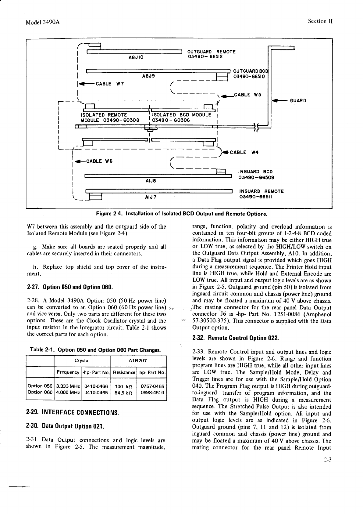
Model3490A
Section
Il
(F
I
I
l<-
f---
rffi
|
-J- --\
I'
I ;+CABLE
i
;<-caBLE
t\
-_
cABLE
TSoLATED
MOOULE
f-1
w7
REMOTE
03490- 60308 | 05490 - 60306
rY6
Figure 24.
IO
A8J
aa,rs
ISOLATED BCD MODULE
:
r-l
AI.J8
7
AIJ
Installation of lsolated BCD
OUTGUARD REMOTE
03490-
- -
/
.
___/
Output
665t2
03490-66510
.
l_J
I
E
and Remote Options.
TNGUARD BcD
JJiJV-99JWt
03490-56511
W4
W7 between
Isolated
g.
cables
this assembly
Remote Module
(see
Make sure all boards are seated
securely
are
inserted in their connectors.
h. Replace top shield
ment.
2-27.
Option 050 and
2-28.
A Model 34904
can
and vice
converted
be
versa.
Only
options. These
input
resistor in
the
correct parts
Table
2-1.
Option
Frequency
Option 050
Option 06O
3.333 MHz
4.000
2-29. INTERFACE
2-30.
Data
0utput
2-31.
Data
shown
in
Output
Figure
Option 060.
Option
to an Option
two parts
are
the Clock
the Integrator
for
each option.
050 and
Crystal
hp- Part
o4100466
MHz
0410{465
CONNECTIONS.
0ption
connections
2-5.
The
and
the
outguard
side
Figure 24).
properly
top
and
050
060
cover
(50
(60
of
Hz
Hz
the
power
power
are different for these two
Table
100
kfi
84.5 ko
crystal
2-1
Part
Changes.
A'1R207
07574465
0@8-4510
Oscillator
circuit.
Option 060
No Resistance +lp- Part No
021.
and logic
measurement
levels
magnitude,
of the
and all
instru-
line)
line)
and the
shows
are
;^.
range, function, polarity
contained in ten
information.
or
LOW true,
the
Outguard
a
Data Flag output
four-bit
This
information
as selected
Data
Output Assembly,
signal is provided
during a measurement
line is HIGH
true.
LOW
in
Figure
inguard circuit
and may be floated
mating connector
._.The
connector J6
true.
while Hold and External Encode
All
input and
2-5. Outguard
common
a
-hp-
is
Output option.
2-32. Remote
2-33.
Remote
levels
are shown in
program
are LOW
Trigger
The Program
040.
to-inguard
Data Flag
sequen@. The
for use with the
output logic
Outguard
inguard
may
be floated
mating
Gontrol
Control
lines
are HIGH true,
true.
lines
are for use
transfer
output
Stretched
levels
ground
common
a maximum
connector
The
Flag
Sample/Hold
(pins
and
for the
and overload information
groups
by the
sequence.
output logic
ground (pin
and chassis (power
maximum of
the
for
Part No.
l-248
of
may be either
BCD coded
HIGH true
HIGH/LOW switch
In
Al0.
goes
which
The Printer
Hold input
levels are
50) is isolated
line)
40 V above chasis.
panel
rear
125l{086
Data
(Amphenol
0ption 022.
input
and
output
Figure 26.
while
Sample/Hold Mode, Delay
with the Sample/Hold
output is
program
of
is HIGH
Pulse
HIGH during outguard-
during a
Output
option.
are as indicated
7, ll
and 12) is isolated
chassis
(power
of 40 V above chassis. The
rear
lines
Range
and
all other
information,
measurement
is
also
All
in Figure 2{.
ground
line)
panel
Remote Input
input
input
is
on
addition,
HIGH
are
shown
as
from
ground
Output
and logic
function
lines
and
Option
and the
intended
and
from
and
:-J
Page 18
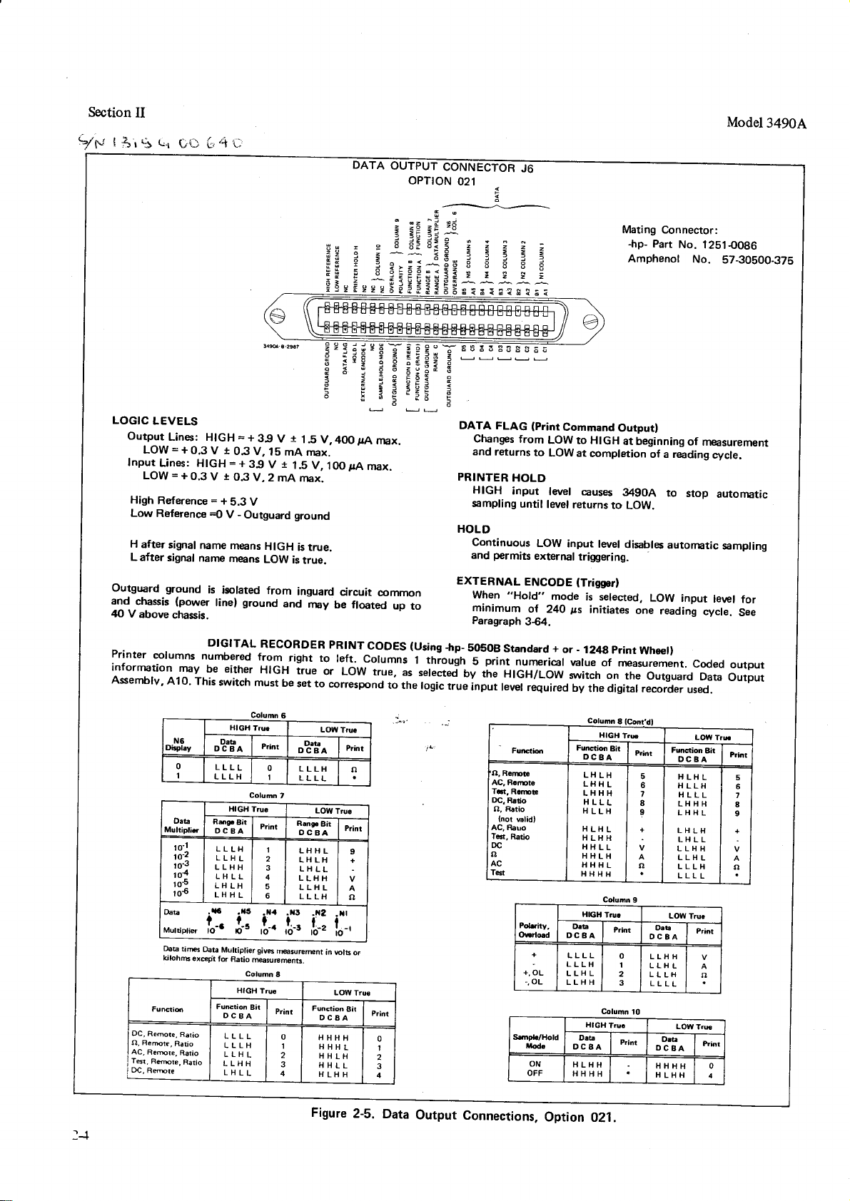
Section
i
7N
3i
LOGIC
Output
Outguard ground
and40
Printer
information
Assenilclv,
II
-s
t**
LEVELS
LOW = +
Input
Lines:
LOW = +O.3
High
Reference
Low
Referenc€
H
after
signal
L after
signal
chassis
V
above
columns
410'
{JrJ
Lines:
0.3
HIGH = +
(power
chassis.
may
This
ü,1t;
=
HIGH
V r
0J V,
r
V
O.3
=
+
5.3 V
-
{ V
Outguard ground
name
means
narne
means
is
isolated
ground
linel
DIGITAL
numbered
be either
switch
+
39 V t
lS
mA rnax.
3.9 V a
V,
HIGH
LOW
1.5 V,
2
mA rnax.
is
from
is true.
inguard
and
RECORDER
from
right
HIGH
i.u"
must
be
set to
z9
:!
;9eFe
1.5 V,4OO
10O
rrA
true.
circuit
,nay
be floated
PRTNT
to
left.
or
LOW
correspond
TA
OUTPUT
:
qi
z
22
?ä;-;03":'
Y
3 EKBö ?
laEFä=;
g
;
COTruECTOR
oPTtoN
äF cö
i: ^j3
6s
Ed
ä
996<
iää
,^j
-8
5
021
DATA
pA
rnax.
max.
Changes
and
PRINTER
HIGH
sampling
HOLD
Continuous
and
EXTERNAL
common
up
ro
When
minimum
Paragraph
(Using
CODES
columns
true,
as
to the
-hp-
through
1
selected
logic
trr"
50508
5
by
t'he
inprt
.IO
=:==
8885
(Print
FLAG
from
returns
permits
Standard *
print
levei
LOW
to
LOW
HOLD
input
le\rel causes
until
level
LOW
external
ENCODE
"Hold"
ol
mode
24O
364.
numerical
HIGH/LOW
required
Command
HIGH
to
at
completion
returns
to
input
tevel
triggering.
(Trigser)
is selected,
ps
initiates
print
-
or
1248
value
of measurement.
switch on
by
the digital
Mating
Connector:
-hp-
Part
Amphenol
Outputl
at beginning
of a reading
349OA
to
LOW.
disables
autornatic
LOW
one
reading
Wheell
the Outguard
recorder
Model34904
No.
1251€086
No.
57-30500-378
of measuremenr
rycle,
stop
autornatic
sampling
input
le\rel
for
cycle.
See
coded
output
Data
Output
used.
l-r
Dkplay
Multiplit
T,i",,*
DaE
kilohG
Fundid
DC,
Re@te,
tl, BemG,
AC,
Remre,
T6t,
Rmte,
OC,
Remre
N6
0
O.ta
to-r
to-2
to-3
to{
to€
'to€
Ratio
Ratio
Ratio
raG
Rario
lJ.
Data
ex@Fit
HlcH
Data
OCBA
LLLL
LLLH
HIGH
Ragr
8ir
DCBA
LLLH
LLHL
LLHH
LHLL
LH
LH
LHHL
i:
Multiplier giv6
for
Ratio
HIGH
Function
DCBA
LLLL
LLLH
LLHL
LLHH
LHLL
Colqmn
6
Tru.
Print
0
I
Colomn
t
Tru.
Print
'|
2
4
5
f: ,1.:
nesurerent
|@iuEments.
g
Column
True
Bit
Print
0
I
2
4
Dat€
DCBA
LLLH
LLLL
Rangr
OCBA
LHHL
LHLH
LHLL
LLHH
LLHL
LLLH
,t;:
Functioo
Figure
LOW
LOW
Bir
;
an rclB
LOW
DCAA
HHHH
HHHL
HHLH
HHLL
H
LH
Trü.
Tru.
Ptint
Print
o
o
8il
H
or
Tru€
2-5.
Print
0
1
3
4
Data
Output
FüfFtkh
O,
Remlo
AC, R.mt€
T6,R.@E
DC.
F.tio
Jl, R.tio
{nor Elidl
AC,
F.r'o
TH,
Ratio
oc
o
AC
T6
Polrity,
Onrlod
+
+,
OL
-.
oL
S..tipb/Hold
Mode
ON
OFF
Connections,
Fundid
D.b
DCEA
LLLL
LLLH
LLHL
LLHH
D.b
DCEA
HLHH
HHHH
Option
Column
HIGH
DCBA
LH
LH
LHHL
LHHH
HLLL
H
LLH
H
LH
HLHH
HHLL
HHLH
HHHL
HHHH
HIGH
Column
HIGH
021
8it
L
Cdumtr
Tru.
Print
o
2
Tru.
.
Tre
1
P.int
I
l0
Print
8
9
+
DCBA
LLHH
LLHL
LLLH
LLLL
Fundion
DCBA
H
H
LHHH
LHHL
LHLH
LHLL
LLHH
LLHL
LLLH
LLLL
LOIV
O.b
LOW
Dü
DCBA
HHHH
HLHH
LOü
LH
LLH
HLLL
Tru!
Print
Tre
L
n
8it
Print
Tr{
Pr&rt
6
7
8
9
+
4
Page 19
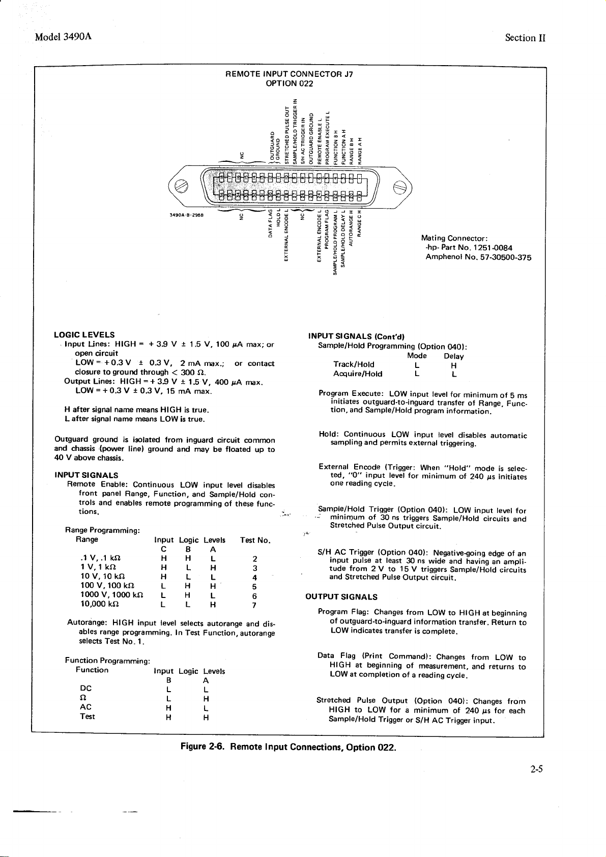
Model34904
Section
II
LOGIC LEVELS
.
lnput Lines:
open
circuit
=
+
LOW
closure to
Output
Lines: HIGH
=
+
LOW
H
after signal name
after
L
signal
Outguard
and chassis
40 V above chassis.
INPUT
ground
(power
SIGNALS
Remote
Range Programming:
front
trols
tions.
Range
.1 V,.1
lV,
10v,
100v.
Enable:
panel
and
1KO
10ko
100ko
HIGH
0.3 V
ground
0-3 V
name
is isolated
linel
Range,
enables
ksl
=
I
through
=
1
0.3 V,
means HIGH
means LOW
ground
Continuous
remote
1000v,1000ko
10,000ko
Autoränge:
ables
selects
Function
Function
DCL
'rlL
ACH
Test
HIGH input
programming.
range
Test
No. 1.
Programming:
34904-B-296a
+
0.3 V,
t
V
3.9
+
39 V
Function,
lnput
1.5
2 mA rnax.; or
<
A.
300
j
i.S
15 mA max.
from
CBA
H H
H L
H
L H
V, 400
is true.
true.
is
inguard circuit
and
may be
LOW input level
and
programming
Logic
L
L H
L L
level
selects
In
Test Function.
Input
Logic
B
H
REMOTE INPUT
"
2-
pA
V,
100
rnax;
contact
pA
nnx.
common
floated
up to
of
these func-
Test
autorange
disables
2
3
4
5
6
7
and
Sample/Hold con-
Levels
L
H
L
H
L
H
autorange
Levels
A
L
H
L
H
CONNECTOR J7
oPTtoN 022
FE
lo
rE=ä;:
t:uE3X:I--
e
52 H * F E I =
qd
E
39H;;5EEiF==
or
No.
dis-
5 fr i F 3 ä
; ? 3
ä-j=!9il
äEHäEä
t:Litr
EF!!A
= Ir
*
-
INPUT
Sample/Hold
Sample/Hold
.*'
iL.
S/H AC Trigger
OUTPUT
Program
Data Flag
Stretched
i ä
6 s
qc
.<
=a
*
SIcNALS
Track/Hold
Acquire/Hold L
Program
initiates
tion,
Hold: Continuous
sampling and
External
ted,
one reading
minirpum
Stretched Pulse
input
tude
and
of outguard-to-inguard
LOW
HIGH at
LOW
Hf
Sample/Hold
Programming
Execute:
outguard-to-inguard
and
Sample/Hold
Encode
"0"
input
Trigger
of
pulse
from
2 V to 15
Stretched Pulse
SIGNALS
Flag:
indicates
(Print
beginning
completion
at
Pulse
to
GH
LOW for
(Cont'd)
LOW input
LOW input
permits
(Trigger:
level for
cycle.
(Option
ns
30
triggers
Output circuit.
(Option
least
at
Output circuit.
Changes
transfer
Commandl:
of
Output
a
Trigger
Mating
-hp-
Part
Amphenol
(Option
Mode
L
level
transfer
program
level
external
040):
30
from
of
or
triggering.
When
minimum
O4O):
Sample/Hold
Negativegoing
ns
wide and
V triggers
LOW to H|GH
information
is
complete.
Changes from
measurement,
a reading
(Option
minimum
S/H AC
Connector:
No.
1251
No.
57-3Ob00-37S
O40):
Delay
H
L
for
minimum
of
information.
,,Hold,,
cycle.
Trigger input.
Range,
disables
mode
of
24O
LOW input
having
Sample/Hold
at
transfer.
and returns
04Ol:
Changes
ot
24O
{O84
of
autornltic
is serec_
ps
initiates
levet
circuits
edge
an
ampli-
circuits
beginning
Return to
LOW to
for
tts
5 ms
Func_
for
and
of an
to
from
each
Figure
2-6. Remote
Input
Connestions,
Option
022.
2-5
Page 20
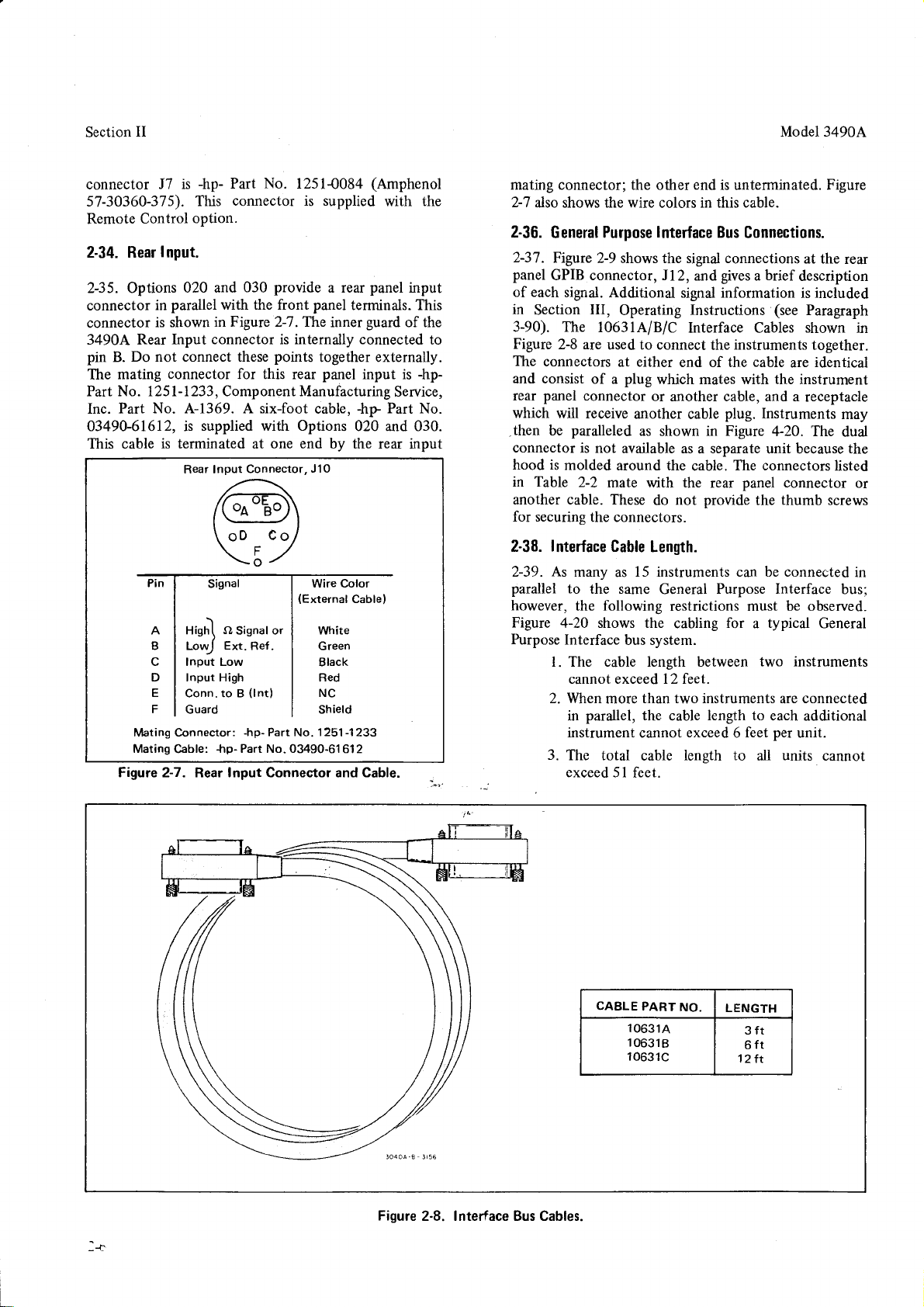
Section
II
Model 3490A
connector
57-30360-375).
Remote
2-34. Rear
2-35. Options
connector
connector
J7 is
Control
Input.
parallel
in
is shown
This
option
020 and
3490A Rear Input
pin
Do not connect these
B.
The
mating
connector
-hp-
in Figure 2-1 . The
connector is internally connected
No.
Part
l25l{084
connector is supplied
provide
030
a rear
with the front panel
inner
points
together externally.
for this rear
panel
(Amphenol
with the
panel
terminals. This
guard
input is
Part No. 125l-1233, Component Manufacturing
Inc. Part
No. A-1369. A six-foot
03490-61612, is
This cable
is terminated
Rear Input
A
High\
B
LoryJ
c
Input Low
D
Input High
tr
Conn. to B
r
Guard
Mating Connector:
Mating
Cable:
supplied with Options
one end
at
Connector,
Signal
)
o
Sisnal
Ext.
Ref.
(lnt)
-hp-
-hp-
Part No.03490-61
or
Part
(External
No.
-hp
cable,
Part
020 and 030.
by the rear input
J10
Wire Color
Cable)
White
Green
Black
Fled
NC
Shield
1251-1233
612
Figure 2-7. Rear Input Connector and Cable.
input
of the
to
-hp-
Service,
No.
mating
2-36.
.then
2-38.
however,
Purpose
connector; the other
2-7
also shows the wire
General
2-37
. Figure
panel
GPIB connector, Il2,
of each
in
Section
3-90). The
Figure
The
connectors
and consist
panel
rear
which
be
connector
hood is
in Table
Purpose
2-9 shows the signal connections
signal. Additional
III,
Operating Instructions
1063IA/B/C
2-8 are
will receive
used to connect
of a
connector
paralleled
is not
molded
around the
2-2
mate with the
at either
plug
another
as
available as a separate
another cable. These
for securing
2-39. As many
parallel
the connectors.
Interface
to
the same
Gable
15 instruments can be connected
as
the following
Figure
4-20 shows the
Interface
bus system.
colors
lnterface
which mates with the instrument
or another cable, and a
shown
do
Length.
General
l. The cable length between
cannot exceed 12 feet.
2. When
parallel,
in
instrument
3.
The total
exceed 5 I
than two instruments
more
the
cannot
cable
feet.
end
is unterminated.
Figure
in this cable.
Bus
Connections.
at the
rear
gives a brief
and.
signal information
Interface Cables
instruments
the
end of the
(see
cable
description
included
is
Paragraph
shown
together.
identical
are
in
receptacle
plug.
cable
cable.
not
in Figure
rear
provide
Instruments
4-20. The
unit because
The connectors
panel
connector
thumb
the
screws
may
dual
the
listed
or
in
Purpose Interface
bus;
restrictions must be observed.
cabling
for a typical
General
two instruments
connected
are
length to
cable
exceed 6 feet
length to
each additional
per
unit.
units
all
cannot
Figure
2-8. Interface Bus Cables.
CABLE
10631A
106318
10631C
PART
NO.
LENGTH
3ft
6ft
'l2tt
Page 21
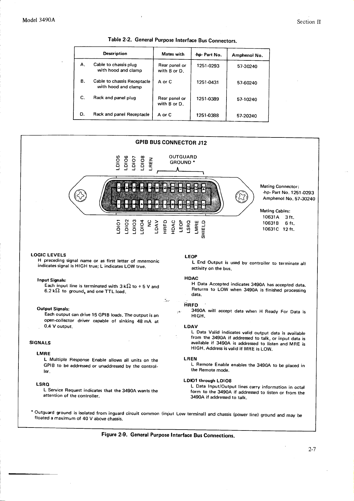
Model
3490A
Table
2-2.
General
Purpose
Interface
Bus
Connectors.
Section
II
A.
B.
a
D.
Description
Cable to
with hood
Cable to
with hood
Rack
and
Rack and
D.
D.
or
or
-hp-
Part
1251-0293
'1251-0431
-0389
1
251
-0388
1
251
Jl2
*
6
No.
Amphenol
51-30240
57-60240
57-10240
57-20240
Mates
with
plug
chassis
and clamp
chassis Receptacle
and clamp
panel plug
panel
Receptacle
GPIB
ro(oF@
9999f
n^^A
JJJJJ
BUS
panel
Rear
with
B or
AorC
panel
Rear
with
B or
AorC
CONNECTOR
OUTGUARD
GROUND
8ä;;'iEFq8ä+
No.
Mating
-hpAmphenol
Mating
10631A
10631
10631C
Connector:
Part
No. 1251
No.57-3O24O
Cables:
3
B 6 ft.
12
4293
ft.
ft.
LOGIC
preceding
H
indicates
Input
Each
6.2 kO to
Output
Each
open{ollector
O.4
SIGNALS
LMRE
L Multiple
GPIB
ler.
LSRO
L
attention
'Outguad
floated
LEVELS
signal
Signals:
input
Signals:
output
V output.
to
be addressed
Service
of the
ground
a maximum
signal
name
is
HIGH true;
line
ground,
can
Response
Request indicates
is
or as first letter
is terminated
and
one TTL
drive 1
S
driver
capable
Enable
or unaddressed
controller.
isolated
of 40 V
from
above
GPI
L indicates
with
3
load.
B loads.
of sinking
allows
that
the
inguard circuit
chassis.
of mnemonic
LOW true.
+
kO to
The output
all units
34904 wants the
4g mA
the control-
by
5 V
and
is
on the
common
an
at
(input
LEOP
L End
activity
HDAC
H
Data
Returns
data.
HRFD
HIGH,
LDAV
L
Data
from the
available if
HIGH.
LREN
L Remote
the
Remote
LDIO1 through
L
Data
form
3490A if
Low terminall
Output
on the
Accepted
to
LOW
Valid
34904
3490A
Address
Enable
mode.
LDIOS
Input/Output
to the
34904 if
addressed
and chassis
is
used
bus.
indicates
when
indicates
if
addressed
is
is
valid if
enables
to
talk_
(power
by controller
34904
34904
valid
output
to
addressed
MRE
is LOW.
the
34gOA to
lines
carry
addressed
linel ground
to
terminate
has
accepted
is finished
data
talk,
or input
to
listen
be
information
to listen
and
data.
processing
is
available
data is
and MRE
placed
in
octal
from
or
may
all
is
in
the
be
Figure
2-9.
General Purpose
lnterface
Bus
Connections.
a1
Page 22
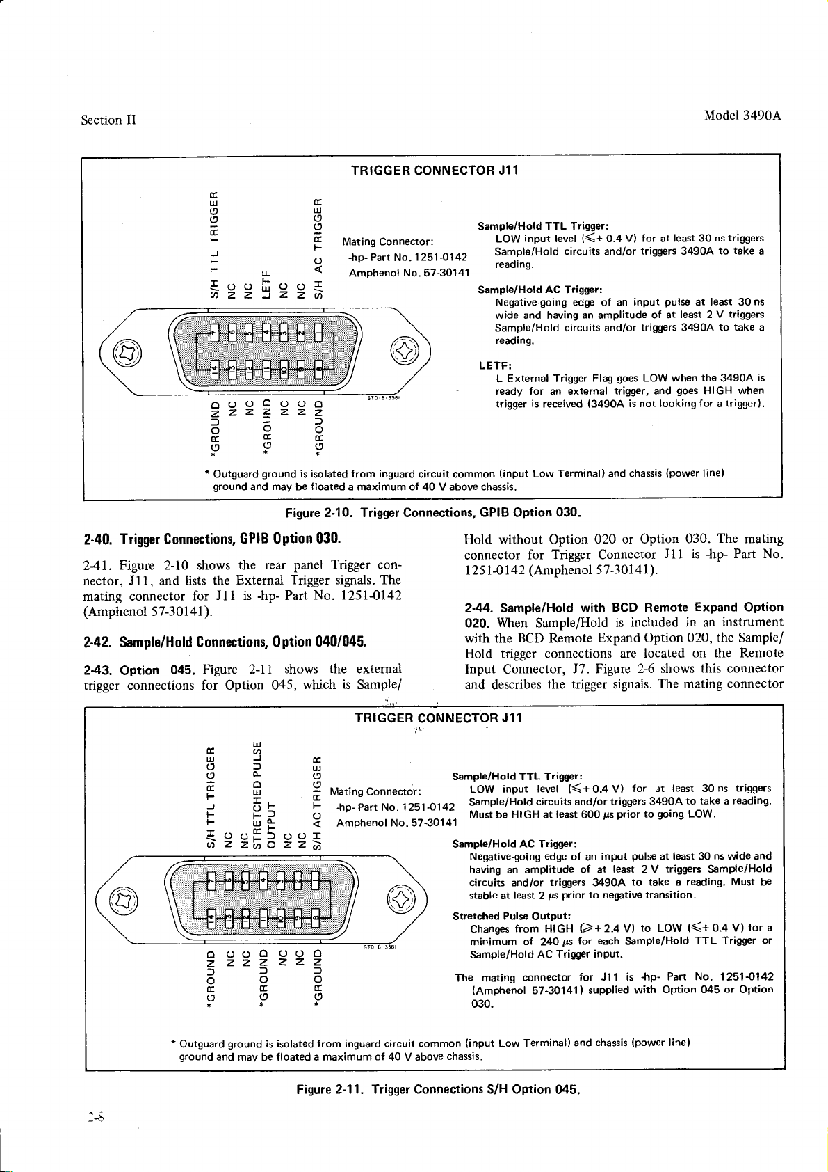
Section
II
Model 3490A
TRIGGER CONNECTOR Jl1
E
UtJJE
!2 lg
9V
=g
FCE
JF
-v
FL
L
Mating Connector:
*rp- Part No.
Amphenol
;22399ä
1251.0142
No.57-30141
Sample/Hold
LOW
Sample/Hold
reading.
Sample/Hold AC Trigger:
Negativegoing edge of an
wide and having
Sample/Hold circuits and/or
reading.
TTL Trigger:
input level
circuits and/or
((+
0.4
an
amplitude
V) for
least 30
at
triggers 34904
pulse
input
of at
triggers
nstriggers
at least 30
least 2 V
3490A
take
to
triggers
to take
a
ns
a
ooooo
zzzzz
zZ
l
tr
*
Outguard
ground
6ö
E6
(9c,
t*
ground
may
and
Figure
Trigger
2-40.
Figure 2-10 shows
241.
nector,
mating
(Amphenol
2-42.
243.
Jll,
connector
57-30l4l).
Sample/Hold
Option
Connections,
lists the
and
for
Connections, 0ption
045.
GPIB 0ption 030.
the rear
External
-hp-
Jll is
Figure
2-ll
Part
shows
trigger connections for Option 045,
EA
IlJIE
\:/JIU
oclo
no(,
F=F
)
!-
: HF
*o(JifC)(Jr
ui
z
l
ol
t-?
z
z'@O zzAi
oooo
2ZZZ
zz
--
ai ,4
**
is isolated from inguard
floated
be
a maximum of 40 V above chassis.
2-10. Trigger Connections,
panel Trigger con-
Trigger signals. The
No. 12514142
040/045.
the
external
is
which
F
()
A
Sample/
TRIGGER
Mating Connector:
part
+rp_
Amphenol
1251*,142
No.
No.57-30141
LETF:
L
ready for an external
trigger is received
circuit common
(input
GPIB
Hold without
connector
1 25 1 41
2-44. Sample/Hold
When
020.
with the
Hold trigger
Input
and
describes
CONNECTbR
Sample/Hold TTL Trigger:
Sample/Hold
Stretched
The mating
Jl1
LOW
Sample/Hold
Must
be
Negative-going
having
circuits
stable
at
Changes
minimum
Sample/Hold
(Amphenol
030.
External Trigger
Low Terminal) and
Option
Option
Flag
(34904
030.
020 or Option
for Trigger Connector
(Amphenol
42
57-301 4
with
Sample/Hold
BCD
Remote
Expand Option
connections
Connector,
J7. Figure 2-6
the trigger signals.
level
input
circuits and/or
HIGH
at
AC Trigger:
edge
an amplitude
Pulse
triggers
and/or
ps prior
least
2
Output:
from HIGH
ot
24O
AC Trigger
connector for
57-30141)
O.4
{(+
least
ps prior
60o
of
input
an
of
at
3490A
to negtive transition.
l2+z.q
each
for
tts
input.
Jl 1 is
supplied
goes
LOW when
trigger, and
is not looking
chassis
goes
(power
030.
Jll is
I
).
BCD Remote
included in an
is
Expand
020,
are
located
on the Remote
shows
The mating
for .)t least 30
V)
triggers 34904
to
pulse
least 2 V
to take a reading.
to
V)
Sample/Hold
*tp- Part No. 1251{142
with
to take a reading.
going
Low'
least 3()
at
triggers
({+
LoW
TTL Triggpr
Option 045
the
HIGH when
for a triggerl.
line)
{rp-
3490A
The
Part No.
is
mating
Option
instrument
the
Sample/
this connector
connector
ns triggers
ns wide and
Sample/Hold
Must
be
for
o.+ V)
or
a
or
Option
*
Outguard
ground
ground
and may be floated a maximum
is isolatedfrom
Figure
inguard
2-11. Trigger Connections S/H Option
circuit
of
40 V above
common
chassis.
(input
Terminalland
Low
045.
chassis
(power
linel
Page 23
Model3490A
Section
II
-hp-
for
J7
is
Part No.
s7-30360-37s).
245.
Sample/Hold
the Trigger
shows
trigger
125
2.46.
signals.
(Amphenol
l-01 42
REPACKAGING
with GPIB Option 030. Figure
Connector,
The mating connector is
57
-301
4 l).
FOR SHIPMENT.
NOTE
If the instrument
service or
identifying
to be accomplished. Include the
serial number of the instrument.
identify the instrument
nulhber. If
-hp-
Sales and Service
247.
The following
the
instrument for
available,
appropriate
tape
or metal bands.
available,
proceed
is to
repair, attach a tag to
the owner
you
have any
place
the
packing
shipped to
be
indicating
and
by model
questions,
Office.
general
is a
shipment. If
instrument
material
If the
follows:
as
and seal
original
1252-0084
Jll,
Hewlett-Packard
the
model
In
any correspondence,
number
contact your
guide
the
original
in
the
(Amphenol
and describes the
-trp-
Part
the
instrument
service
or
number
for
container
well with strong
container
and full
and
full serial
nearest
repackaging
container
2-10
No.
for
repair
with
is not
a. Wrap
before
b. Place
instrument
plastic
or
c. Place
heavy
d. Mark
MENI"
If
Hewlett-Packard
o tag
owner
be accomplished.
is
and
any
by
you
est
the
instrument
placing
carton
in
an inner
packing
and protect
foam.
the
instrument
and seal
shipping
"FRAGILE."
the
instrument
to
the instrument
and indicating
seiul
number
any
Sales
number
questions,
and Service
full
cotrespondence,
model
have
-hp-
in
heavy paper
container.
material
with strong tape
container
etc.
for
Include
and
around
panel
face
with cardboard
and inner
'.DELICATE
NOTE
is to
be shipped
service
or repair,
identifying
the service
the
model number
of the instrument.
identify
full
contact
Office.
the
seriat
all sides
container
or
metal
attach
the
or
repair to
instrument
nimber.
your
near-
or
plastic
of
the
strips
in
bands.
INSTRU_
to
In
If
a
2-9
Page 24
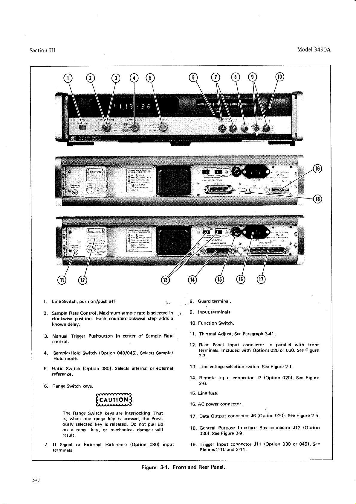
Section
III
Model3490A
1.2.Line
Switch,
Rate Control.
Sample
clockwise
known delay.
Manual Trigger
J.
control.
4.
Sample/Hold Switch
Hold mode.
Ratio
5.
6.
Switch
referen@.
Range
Switch
The
Range
is,
when
ously selected
on a range key,
result-
a
Signal or
terminals.
push
on/push off.
position.
Maximum sample rate is selected in
Each
Pushbutton in
(Option
(Option
keys.
one range key
0801. Selects
keys are
Switch
is
key
or
External Reference
counterclockwise
center
of Sample
o4o/045).
is
released.
mechanical
Selects Sample/
internal or
interlocking.
pressed,
not
Do
damage will
(Option
Figure
step adds a
external
That
the Previ-
pull
up
O80l input
.'^".
Rate
31.
.
._.8.
9. InPut
i\-
10. Function Switch.
1.
1
'|
2. Rear
1 3. Line
14.
1
5. Line
16, AC
17. Data Output
18.
19. Trigger
Front and
Guard terminal,
terminals.
Thermal Adjust. See
Panel input connector in
terminals. Included
2-7.
voltage selection switch.
Remote
2-6.
General
030).
Figures 2-l0
Input connector J7
fuse.
power
@nnector.
connector
Purpose
Figure 2-9.
See
connector J1 l
Input
and2'11.
Inter{ace
Rear Panel.
Paragraph
with
Options 020
(Option
J6
3-41.
parallel
gee
Figure
(Option
0201.
connector J12
Bus
(Option
with
or
030. See
.
2-1
0201. See
Figure
See
030 or 045).
front
Figure
Figure
2-5.
(Option
See
l-rJ
Page 25
Model3490A
SECTION III
Section
III
INTR0DUCTI0N.
3-1.
section
This
3-2.
34904
Model
resistance
and
sample/hold
for
tions
control
may
the
3.3.
3-4.
3-5.
voltage,
S-digit resolution
except
ranges,
1000V; and
Ranging
and display
which
3-6. Output
3-7.
Option
coded decimal
either HIGH true or LOW true,
switch
assembly. With
function may be
information.
option.
3-8. General Purpose
030. The
option
the same
bus in parallel
controlled
control
mode
includes
tude
Controlling
3490A
calculators
Programmer.
3-9.
3-10.
\todel 3-190.{
and
found
be
front
3490A
INSTBUMENT
Standard
standard
The
ac
l000Vac
V
.l
may be
checks
Data
Output
022. Option 021
on
General Purpose
permits
bus lines. The 3490A
by
of range,
possible
is
measurement
and range,
GPIB option
Sample/Hold
The
Sample/Hold
contains
Multimeter
measurements.
output.
data
pull-out card at
a
on
Panel.
CAPABI
I nstrument.
Model
voltage
are
and Remote Gontrol 0ptions.
the
instruments
and
and resistance
and
to
dc.
1000V;
to
six resistance ranges,
manual
automatic.
certain operations within
Option
(BCD)
outguard data output
Option
programmed
External
remote
with several
a single
function,
with
in the
the
0ption
Multimeter
instructions
to make dc
It
and ratio
Basic operating
LITIES.
3490A Multimeter
to I 20 % of range on all
up
3490A
The
4 ac
or automatic. Polarity
A self-test feature is included
021
provides
output data.
O22, the
triggering
Interface
Interface
programmhg
controlling instrument.
trigger mode and sample/hold
Option 030.
status,
function,
format
-hp-
given
that may be used with the
include
Model 3260A
040
or
Option
(040
to sample a changing input
OPERATING
for using
voltage, ac voltage
includes
also
measurements, remote
instructions
the
bottom edge
measurements with
has five dc
voltage ranges,
I kO to 10,000kQ.
the instrument.
and Remote
columns of
ten
This
data
as selected by
printed circuit
349OA
by LOW
possible
is
Bus ll0
and data
may be
other
in Paragraph
-hp-
the
true
with
Bus I/O
connected
instruments and
The output data
polarity, magni-
9800A
Marked Card
045.
or
045)
the
instruc-
makes dc
ranges
voltage
I V to
selection
Control
binary
may be
slide
a
and
range
input
either
Option
(GPIB)
output on
to
Remote
3-126.
series
enables
the
INSTRUCTIONS
voltage
amplitude. This
digitization of
waves.
signal input Low terminal and from chassis
which allows the voltmeter
measurements. The
of
Sample/Hold options are as
When Sample/Hold
3-11. Batio
3-12.
capable of making three-wire dc-to-dc
measurement. Two External Reference ranges are pro-
vided, the I V
10.1
voltages from
3.13.
3-14. Figure 3-l
and connectors
Some of the features shown
certain options.
,.
3-15.
3-l 6.
between
a
chassis. These maximum
front
instrument
and hold
The
extemal
in a 3490A with:
BCDiRemote
GPIB
Option
Neither 020 or
0ption
The 3490A
t 1.2V,
V to
t
FRONT AND
MAXIMUM INPUT
Table 3-l
input terminals,
panel
and
may
If the
34904 has a rear
the
front
connected
be applied, always
nals. Be
before connecting
open
terminals
front
sample
that
permits pulse
changing
trigger circuits are
designations
is
installed
Expand
030
030
long enough to measure its
height measurements and
waveforms
follows:
Option 020
such
to
make
used for the
The
Sample/Hold
is designated as:
Option 040
Option
Option 045
080.
equipped with Ratio Option
range accepting reference
the 10V
and
I V to t 12V.
PANEL
REAR
shows the front and rear
gives
and
a brief
OESCRIPTION.
description
are available
VOLTAGES.
the
lists
must
resull.
maximum allowable voltages
and between the
voltages are
not be exceeded or
also
wAR]ililG
input connector,
and rear terminals are
puallel.
in
the rear input
ilre
If
protect
and vice
voltages may
high
the open
terminals
input to
an
versa.
as ramps or
isolated
guarded
040
or
ac-to-dc ratio
range accepting
panel
terminals
shown
damage
internally
termi-
sine
from the
ground,
floating
34904
option
080
voltages of
controls
of each.
onlv
with
and
on the
to the
are
the
is
3-l
Page 26
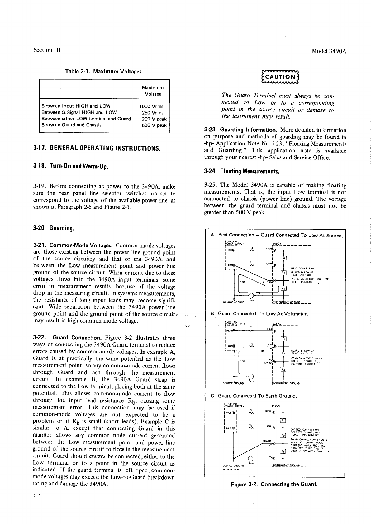
Section
III
Model
3490A
Table
3-1 .
Between Input
Between fi
Between
Between Guard
3.I 7. GENERAL
3-18. Turn-On
3-19. Before
sure the rear
correspond to the
shown
in
HIGH and LOW
HIGH and
Signal
either
LOW
and
OPERATING
and
Warm-Up.
connecting
panel
voltage
Paragraph
Chassis
2-5 and Figure 2-1.
3-20. Guarding.
3-21. Common-Mode
are those
of the source
between the
ground
voltages
error in
drop in
the resistance
cant.
ground
may
existing between
circuitry
Low
measurement point
of the
source
flows into
measurement
the
measuring
of
long input
Wide separation
point
and
the
result in high
common-mode
the 3490A
Maximum
terminal
LOW
and
Voltages.
Guard
Maximum
Voltage
100O
Vrms
250 Vrms
2O0 V
500 V
INSTRUCTIONS.
power
ac
line selector
of
Voltages. Common-mode
the power
and that
circuit. When
results
circuit. In systems
between
ground
to
the 3490A,
switches
the
available power
of
current
line
the
and
are set to
ground
34904,
power
due
input terminals, some
because
of the voltage
measurements,
leads
may
become signifi-
the 3490A
point
of the source
power
voltage.
peak
peak
make
line
as
voltages
point
and
line
to
these
line
circuiü,
The
Guard
nected
point
the instrument
3-23.
Guarding Information.
on purpose
-hp-
Application
and
Guarding."
through
your
Terminal
to
Low
in the
and
methods
Note No. 123,
This
nearest
-hp-
must
or to
source
moy
circuit
result.
More detailed
guarding
of
"Floating
application note
Sales and
3-24. Floating Measurements.
3-25. The
measurements.
connected
between
geater
the
than
A. Best
Connection - Guard
r---
B.
Guard Connected To
Model
That
to
chassis
guard
500
3490A
terminal
peak.
V
is
capable
is,
the input
(power
line)
and chassis must
Connected
44904
--------
Low At Voltmeter.
always
be
con-
a corresponding
or damage
information
may
be found in
Measurements
is
available
Service Office.
of making flöating
Low terminal
ground.
The
voltage
not
To
Low
At
Source.
- -
CONNECITON
EEST
SAME VOLTAGE
NO COMMON MOOE
GOES
9!9!'!-9 _ _ _
IHROUGH
CURRENI
Rb
to
is not
be
3-22.
ways
errors caused
Guard is
Guard
Connection. Figure
of connecting
by common-mode
practically
at
measurement point,
through
circuit. In
connected
potential.
through
measurement
common-mode
problem
similar to
manner
between the
gound
circuitLou' terminal
rrdicated.
mode
r3ring and
Guard
example
to the
This
the input
or if
A.
allows
of the
Guard
If
the
voltages
damage
and not through
Low
allows
error.
voltages
R6 is
except
any
Low
source
should
or
guard
may
the
3-2 illustrates
the 3490A
Guard terminal
voltages.
the same
potential
so any common-mode
the
B,
the
3490A
terminal, placing
common-mode
lead
resistance
This
are
small
connection
(short
R6, causing some
not
expected
leads). Example
that connecting
common-mode
current generated
measurement point
circuit
to flow in the
alwoys be connected,
to
point
a
exceed
in the
terminal
the
Low-to-Guard
source
is
left open, common-
34904.
three
to
reduce
In example
as the
current
A,
Low
flows
measurement
Guard strap
both
at the
same
current to
flow
may be used if
to
be a
C is
Guard in this
power
and
line
measurement
either to the
circuit
breakdown
is
as
C. Guard
FLOATING
r'-
i*.J
Connected To
- -l
3-2.
Figure
VOLIACE
sÄME
Earth
COMMON MOOE
6OES TBROüGH
CAUSIN6
9E0!{q__
Ground.
DOITEO
DEFEAIS
OAMACE INSIqUMENT
SOLIO
MUCH
CURRENT AWAY FROM
PROVIDED
MOSILY
GROUNO
CURRENT
ERRORS
_
CONNECIION
GIAROI MAY
CONN€CION
OF
COMMON MOOE
THAT
8€TWEEN
Fb,
ECM
Connecting the Guard.
SHUNTS
Rh,
15-
GROUNOS
Page 27
3490A
Model
Section
III
0verrange
3-26.
3-27. Measwements
to 120
up
ranges. Overrange
the maximum
includes the overrange
3-28. Overload
3-29. lf the
the
Overload
display will read
Bange
3-30.
The 349OA
3-31.
kilohms
decimal
selected. In
indicates
3-32.
3-33.
by the function
control
indicate
available
TST
(except
point
range.
Function Indication.
In the standard
is in use,
that the
special
annunciators
Measürements.
of runge
7o
inputs on
allowable
Indication.
measurement
"OL"
annunciator will
120000 to 120005.
Indication.
in
and
autorange
switch position.
the
front
display
to
rated
within
on all except the
these
input
"1"
display always
Ratio
range switch
mode, the
3490A,
"REM"
panel
assembly
indicate
voltage.
the sixth
as
is 120
%
measurements),
function is
annunciator
switches
adds V,
the
function
accuracy
ranges
of
light.
reads
indicating
decimal point
If
are
1000
would
The
digit.
nnge
The
in volts
indicated
optional
are
disabled. An
AC,
selected.
Vac
or
numerical
with the
the
lights
possible
or
exceed
display
geater,
range
alone
only
Remote
to
Kfl
and
dc
or
a.
Set
Function
Sample/Hold
SAMPLE/HOLD
b.
Set
SAMPLE
wise from
c.
should
in
the
with
shown.
count
The,last
to
logic
d.
t
2 counts.
HOLD.
Select
_follow
list.
All
the polarity
The
accumulates,
two
the
test.
circuits
Select
This
RANGE
last
digits in
If
are
RANGE
options,
to
the
sequence
readings
sign,
reading
these
operating
+
080.024
+
o4.oo24
+
0.20024
+
.0too24
+
0.09032
+
to.oo24
+
200.024
+
4000.24
+
80002.4
+
6000.xx
verifies
to TEST.
set
OFF.
RATE
l,
which
should
numbers,
listed
then
stops
the last
displays
correctly.
OL
2.
The
the
l0
If
instrument
RATIO
control
below,
number
to
INT
one position
is
Logic
Test.
starting
in
be
the
and
decimal
displays
at the
are correct,
all
number
are not
display should
V range
zero.
has
Ratio
REF
and
clock-
The
display
at
any point
order
ih-own,
points
digiis
as
the
shown.
significant
most
of the
be .000000
or
ai
Autoranging.
3-34.
3-35.
In
the autorange
of
range and
ment sequence
the proper
control
button
sample
When
a voltage
valid.
3-36.
3-37.
When
measurement
depressed.
instrument
sampling
3.38.
3-39.
proper
circuits,
procedure
not
correct,
of the
mance
range.
is set
depressed
until
the
3490A
range,
ManualTrigger.
Manual
the
Sample
If
is
will stop
SELF.TEST
The
Intemal
operation
and
the
to perform
refer
other
tests
Checks.
mode,
downranglng
is
not
completed
For
example,
to
Hold
and the
once,
the 3490A
one
reading
is
changed
the
first
triggering
results
the
not
is
Rate
control
each
time
pushbutton
in
the
until
the
OPERATION.
Test
function
of
most
ohmmeter
the
Intemal
to
the
Troubleshootingsection.
are
not
upranging
lOVo
at
unless the
is
taken
to the
reading
available
the Manual pushbutton
is
Hold
button
of the
reference.
correct,
occurs at l2O%
of
range. Ameasure-
reading
if
the
Sample
Manual Trigger
will continue
on
the correct
autorange
in
autorange
on
instruments.
all
is set to
depressed
condition,
is released.
of
the 3490A
dc
circuits,
Use
the
Tests.
If
Test
refei to
is
Rate
push-
range.
mode
from
is not
Hold,
while the
automatic
verifies
logic
following
No. I
Ifany
perfoi_
the
on
to
one
ii
e.
Select
RANGE
readings
accuracy
+
3490A
l0 V
shoüld
dmplifier
position
'counts,
is
accuracy
-
10.0000V.
+
attenuation
Dsplay
proper
3-40. DC
341.
.l V
should
f.
Select
RANGE
of t
10.0000
dc standard
V. Display
error).
has the
and short
be r
00.0000.
zero.
and
remove
g.
Select RANGE
verifying
h.
Select
RANGE
of t
Display
dc standard
and
i.
Select
RANGE
should
operation
VOLTAGE
For
optimum
range,
first
be
error).
the dc
be
3.
(8
0.01
ratio
EXT
Return
the
0.01
-
09700.0 1
of the
Difference
counts.
4.
Using
a
% or better,
should
be + 09.9990
This
checks
option,
REF
This
set
input
checks the
RATIO
short
from
input.
5. Display
0.1 V range
6. Using
should
zero.
a dc standard
% or better,
should
be - 1000.00
This
ehecks
amplifier
7.
Short fl
xl00
7000 counts.
Ohms
Converter.
MEASUREMENTS.
short
accuracy
the
of measurements
input
terminals
between
dc standard
apply
an
+
(16
+
the
Reference.
RATIO to
EXT
terminals.
Ratio
switch
be
apply
the
dc input
to INT
000.000 t
an input
(35
I
gain.
SIGNAL
This
with a copper
+
having
input
Reference
having
terminals.
and
an
of
counts
Ifthe
REF
Display
REF
t5
an
of
counts
0.01
verifies
the
on
-
J-J
Page 28
Section
III
3490A
Model
or a large
bar
(Thermal Adj)
through
connector,
the rear
loosen
AlR429.
Be wre
to observe
and
tations
3-1,
Table
rewlt.
may
DC Sample
3-42.
sample
The
3-43.
measurements
3-2. Sample
Table
Function
Volts
DC
Volts
AC
Ohms
k thru
.1
100
1,O00
10,000
*Sample
not in
Option
3-44.
240.2ms+5ms
1.26s+.025s
ko
240.2ms+5ms
kf,,
300.2ms+6ms
ko
660.3
Rate Control
overload.
050 instruments,
Input Resistance.
solid
zero
for
panel.
the
connect
to
copper
wire, and
display.
the
If
hinged
the Guard
the maximum
the
on
noted
damage
or
Rate
rate and
shown in
are
Minimum Sample
050
Option
ms + 12 ms
set to
Each counterclockwise
front
Response
and
response
Table
and Response
Rate
FAST
ms in
200
adjust
AlR429
to
the rear
gain
3490A has
cover
Terminal
voltage
panel
ta the
instrument
Time.
for dc
time
3-2.
Period*
O60
Option
ms+4ms
200.1
1.05s+.025s
ms+4ms
200.1
ms+5ms
250.1
ms + l0
550.2
position
Option
and instrument
adds
step
060
AlR429
is
accessible
input
access
limi-
in
and
voltage
Time.
Response
Time
200.1
1.05 s
2OO.1
25O.1
ms
550.2
ms
240
instruments.
in
to
ms
ms
ms
ms
Frequency
3-50.
Frequency
3-51.
250kHz,
That
is 2OHz
100
3-52.
3-53.
all
r"itft u
is, the frequency
to 250
is 100 kHz,
V
Input lmpedance.
Input impedance
ranges,
and
instruments
instruments
Harmonic
3-54.
The
3-55.
circuit
verter
sinusoidal
input
ments
input.
signal
as shown
Harmonic
Any
even
Bange.
range
maximum
kHz, but
and at
is 2 MO
without
having
D istortion.
3490A
calibrated
Therefore,
will affect
in Table
Table 3-3.
%
is
converter
the ac
of
range
volt-Hertz
for
the
product
I V and
the maximum
l0 kHz.
it is
V
1000
function
ac
in the
panllel with
in
t I
%
panel input
rear
tire rear
panel
input
connector'
has an average-responding
to display
any
the rms
distortion
the accuracy
20Hz
l0
V ranges
frequency
is the
(
(90pF
and
ac-dc
value
present in the
of the
3-3.
Distortion
Distortion
o.1
0.5
1.0
2.O
Error.
Yo Error
{*Fundamental)
Max.
Positive
0.000
0.001
0.005
0.020
Max.
Negativr
to
of 107.
at
same on
pF
65
in
in
conof a
measure-
Input resistance
345.
o
ohms on
101
t
megohms
3.46.
0.1 5
AC VOLTAGE
Be sure
to observe
and
tations
noted
Table 3-1,
result, and
may
will
ments
The display
341 .
the input shorted.
with
the input
accuracy
shorted should be
of ac measurements
not specified.
AC
3-48.
-3-49.
Sample
The sample rate and
measurements
function
the dc
in
I V, and
V,
the .1
7o
the 100
on
V and
MEASUREMENTS.
connect
to
or
be
will NOT
Rate and
are shown
the
the maximum
the
on
damage
high
front
to
frequency
in enor-
rcad
The indication
less
below
Response
response
nTable
is
10V ranges,
1000 V
Guard
Terminal
voltage
panel and
instrument
the
measure-
on any
zero
on all
50 counts.
than
of full
1.0%
Time.
time for
3-2.
greater than
l0
and
ranges.
limL
in
ac range
with
ranges
The
range is
voltage
ac
Third
Fifth
*Depends
fundamental.
RESISTANCE
3.56.
When the
3-57.
ments,
display
movement
readings
mtusur.*ents
Function
copper
efn+zq
accessible
rear
access
to
bar
(Thermal
through
connector,
input
the adiustment.
to
on
on
.1V
or
phase
0.1
o.5
1.0
2.o
0.1
o.5
1.0
2.O
relationship
o.033
68
0.1
0.338
0.687
0.020
0.1 01
0.205
o.420
between
MEASUREMENTS.
3490A
of the
jump.
to
the .1
dc, short
solid
large
Adj)
rear
the
loosen
is making
instruction
For
kO
the
for
panel.
resistance
optimum
first
range'
input
copper
display'
zero
If the
the hinged
0.003
o.167
0.328
0.667
0.020
o.099
0.195
1.380
harmonic and
measure-
will
card
accuracy
Range
set
terminals
wire, and
A1R429
3490A
cover
cause
with
adjust
has
gain
to
of
and
a
is
the
Page 29
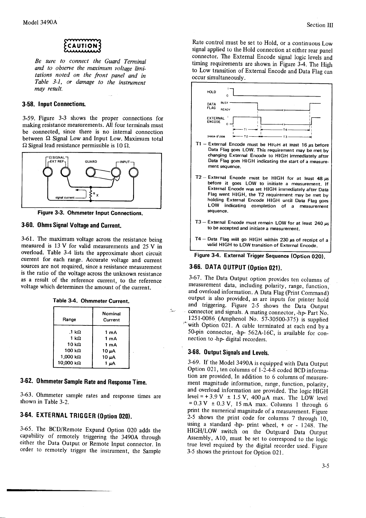
Model3490A
to connect
sure
Be
and to obserye
tations
Table 3-1
may
3-58.
3-59.
making resistance
be connected,
between
O
Signal
noted
,
result.
Input Connections
Figure
3-3
since there
O
Signal
lead resistance
O SIGNAL
the
the
maximum
on the
or damage
shows
front
to
the proper
measurements.
is
Low and Input
permissible
Guord
voltage
panel
the
Terminal
limi-
and
in
instrument
connections
All four terminals
no internal
Low.
connection
Maximum total
is 10 O.
for
must
Rate
control
signal
connector.
timing
to
Low
occur
must
be set
applied to
The
the Hold
External
requirements
transition
of
simultaneously.
HOLD
are shown
External
Pilä:::",----__1_
,
o
Encode
goes
Flag
External
goes
Flag
sequenoe.
must be
LOW.
HIGH
Tl
-
EXTERNAL
ENCODE
34904.81&
External
Data
changing
Data
ment
to Hold,
connection
Encode
Encode
HtLiH at
This
requirement
Encode
to
indicating
or
a continuous
either
at
signal
in Figure
and Data
teast
HIGH
immediately
the
start of a
Section
rear panel
logic levels
34.
The
High
Flae
r
ps
16
rnay
before
be met
after
measure-
III
Low
and
can
by
Figure
3-3.
Ohmmeter lnput
3-60. 0hms Signal
3-61.
The
maximum
measured
overload.
current
sources
is the
as a
voltage
3-62.
3_-63.
shown
3-64.
365.
capability
either
order
is 13
V for
Table
3-4
for each
are not
ratio
result
which
0hmmeter
Ohmmeter
in
Table
range.
required,
of
the voltage
the
of
determines
Table
34.
Range
10
100
1,000
10,000
Sampte
sample
3-2.
EXTERNAL
The
BCD/Remote
of
remotely
the
Data
Output
to
remotely
Voltage
and
voltage
valid
lists the
across the
measurements
approdmate
Accurate
since
a resistance
across
reference
current, to
the
amount
Ohmmeter
ko
.l
lko
ko
ko
ko
ka
Rate
and
rates
TRtcGER
(Option
Expand
rriggering
or
Remote
trigger
the
Connections.
Current.
resistance
and 25 V in
short
voltage
measurement
the unknown
the
of the currenr.
Current.
Nominal
Current
1mA
lmA
lmA
pA
10
pA
10
1
ttA
Besponse Time.
and
response
020).
Option
instrument,
020 adds
the
3490A through
Input
connector.
circuit
and
current
resistance
reference
times
the
Sample
being
are
the
In
T2-External
before
External
Flag
holding
LOW
sequence.
T3 - External
to
T4 - Data
valid
Figure
3-4.
3-66.
DATA
3-67.
The
measurement
and
overload
output
and
.
connector
1251-0086
.
"
with
50-pin
nection
3-68.
3-69. If
Option
tion
ment
and
level
=0.3V
print
2-5
using
is
triggering.
Option
connector,
to
Output
the
02l
provided,
are
magnitude
overload
=
+
3.9
+
the
numerical
shows
a standard
HIGH/LOW
Assembly,
true
level
3-5
shows
Encode
goes
it
Enmde
went
HIGH, the
External
indicating
Encode
be accepted
Flag
HIGH
and
go
will
to
LOW transition
External
0UTPUT
Data
Output
data,
including
information.
also provided,
Figure
and
signals.
(Amphenol
021
-hp-
Signals
Model
,Ien
information
V r
0.3V,
the print
switch
Al0,
required
the printout
A mating
. A cable
-hp-
digital
recorders.
and Levels.
3490{is
columns
In
addition
information,
1.5
V,
l5mA
magnitude
code
-hpon
must
be
by the
for
müSt
be HIGH for
Low
to initiate
was
set HtGH
T2 requirement
Encode
completion
must
rernain
initiate
HIGH
Trigger
(Option
immediately
HIGH until
LOW
a rEasurement.
within
of External
Sequence
021).
option provides
polarity,
A Data
as
2-5
Flag (prini
are inputs
shows
connector,
No.
57-30500-375)
terminated
562A-16C,
is
equipped
of l-24-8
coded
to
6 columns
range,
provided.
are
pA
400
max.
max.
Columns
of a measurement.
for columns
print
wheel,
the
Outguard
set
to correspond
digital
recorder
Option
021.
at
least
a measurement.
rnay
Data
of
a measurement
for
at least
ps
230
of receipt
(Option
ten
range,
4gps
after Data
met
be
Flag
24O
Enc,ode.
020).
columns
function,
goes
of a
Commandj
for printer
the
Data
-hp
hold
Output
part
No.
is supptied
at each .nä'by
available
with
Data
BCD
of
for
con-
Output
informa-
measure-
function, polarity,
The logic
The
LOW
I
through
HIGH
level
Figure
7 through
+
or - 124g.
Data
to
used.
10,
The
Output
the logic
Figure
lf
by
ps
of
u
6
3-5
Page 30
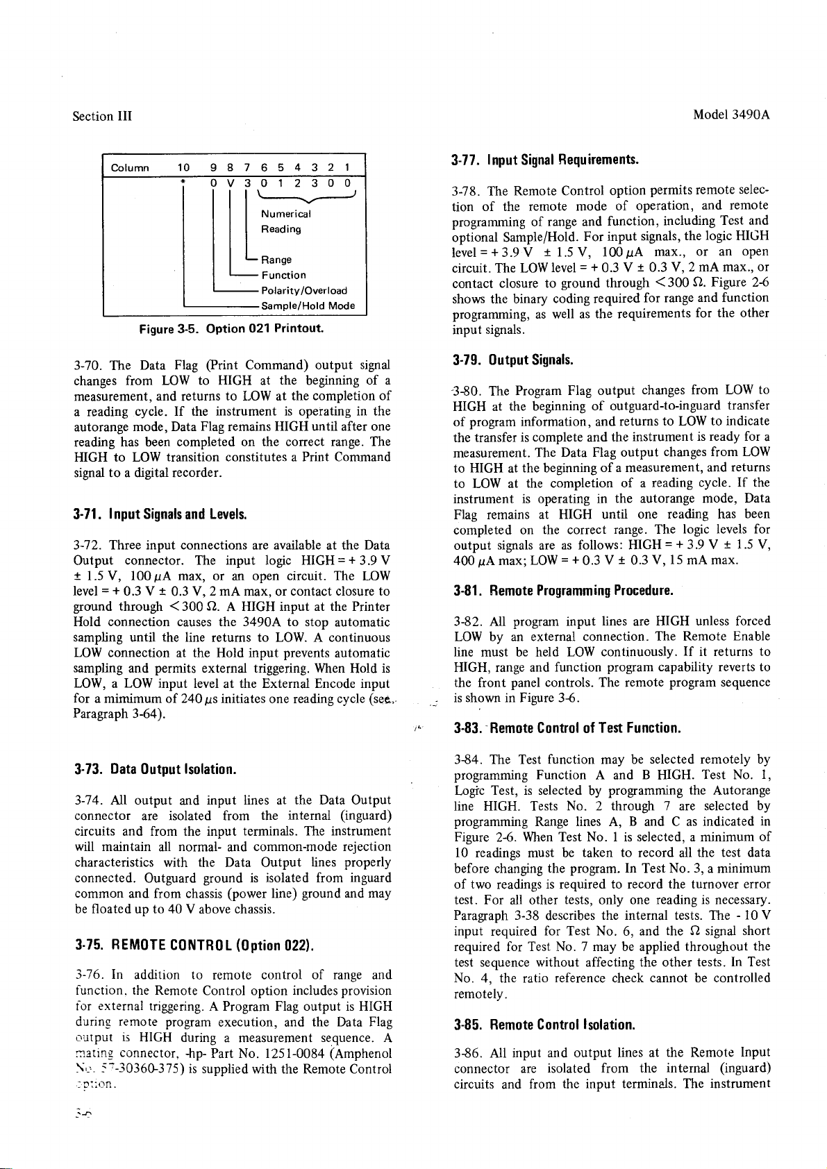
Section
III
Model34904
Column
-_-_ll-
3-70.
The
changes
measurement, and returns
a reading
autorange
reading
HIGH to LOW
signal to a digital recorder.
3-71.
3-12. Three input connections
Output
+
level
ground
Hold connection causes the 3490A to stop
sampling
LOW
sampling
LOW, a LOW input
for
Paragraph
from LOW to HIGH at
cycle. If the
mode, Data
has been completed on
Input
connector. The input logic HIGH
1.5V, l00pA max, or
=
+
0.3 V
through <
until
connection
and
a mimimum of 240
3-64).
10
947654321
0v3012300
l+
Numerical
I
Readino
I
L
*"nn"
F unction
Polarity/Overload
Sample/Hold
Printout.
3-5. Option
Figure
Flag
Data
Signals
t
the
permits
@rint
Flag
transition constitutes a Print Command
and
0.3 V.
A.
300
line returns to
the Hold input
at
external triggering. When
level
ps
021
Command) output signal
the
beginning
to LOW at
instrument is
remains
the completion of
operating
HIGH until after one
the correct range. The
Levels.
available
are
open circuit. The
an
2 mA max.
A HIGH
the External Encode input
at
initiates
contact closure to
or
input at the Printer
A continuous
LOW.
prevents
one reading
Mode
of a
in the
the Data
at
=
+
3.9 V
LOW
automatic
automatic
Hold
cycle
is
(see.
Input
3-77.
3-78. The Remote
of the remote
tion
programming of
optional Sample/Hold.
=
+
level
circuit. The LOW
contact
shows the binary
programming,
input
3-79.
-3-80.
HIGH at
of
the
measurement.
to
to LOW at
instrument
Flag remains
completed on
output
400
3-81.
3-82.
LOW by an external connection.
line
HIGH, range and
the
is shown in Figure 3-6.
3.9 V
closure to
signals.
0utput Signals.
Program
The
the beginning
program information, and
transfer is
HIGH
at
signals
max; LOW
l,rA
Remote Programming
program
All
must be held
panel
front
3-83.'Remote Gontrol 0f
Requirements.
Signal
Control
range and
r
1.5
level
ground
coding required
as well as
Flag output
complete
Data Flag output
The
the beginning
the completion
is operating in
at HIGH until
the correct
as follows: HIGH
are
=
input
LOW continuously.
function
controls. The remote
option
mode
function,
input
For
100
V,
=
+
0.3
through
the requirements
of outguard-to-inguard
the
and
of a measurement,
+
V r 0.3
0.3
lines
program
Test Function.
operation,
of
pA
t
V
returns
instrument
of a
the autorange mode,
one reading has
range. The
Procedure.
are
permits
signals,
0.3 V,
for range
changes from LOW
reading cycle.
V,
remote
including
the
max.,
The Remote
or an
2 mA max.,
<300 O.
for the other
to LOW to
is ready for
changes from LOW
logic levels for
=
+
3.9 V
l5
mA max.
HIGH unless forced
If
capability reverts to
program
selec-
and remote
Test and
logic
HIGH
open
Figure 26
and function
transfer
indicate
and returns
If the
Data
been
t
1.5 V,
Enable
it returns to
sequence
or
to
a
Data
3-73.
3-74. Nl output
connector are isolated from
circuits
will
characteristics
connected.
common
be floated up to 40
3-75.
3-76. In
iunction. the Remote
external
for
during
rrulput
:natinE
\-' r:-3036G375)
.t
ol:on.
la
0utput
and from the input
maintain
and from chassis
REMOTE
addition to
remote
is
HIGH
connector.
lsolation.
input lines at the Data Output
and
normal-
all
with
Outguard
C0NTROL
triggering.
program
during
and
the
Data Output
ground
(power
V above
chassis.
(0ption
remote control
Control option
A Program Flag output is HIGH
execution, and
a measurement
*rp- Part No. 125 l-0084
is suppliedwith
terminals. The instrument
the internal
common-mode rejection
isolated
is
line)
(inguard)
lines properly
inguard
from
ground
and may
022).
of range
includes provision
the Data Flag
se,quence.
(Amphenol
the Remote Control
and
3{4. The Test function may be
programming Function
Logic Test, is selected
line HIGH. Tests
programming
Figure
l0 readings must be
before changing
of two
test. For
Paragaph 3-38
input
required
required for Test No. 7 may be applied
test sequence without affecting the other
No.
4, the ratio
remotely.
Remote Control
A
3-85.
336. All input
connector
circuits
Range lines A, B and C as
When Test No. I is selected, a minimum
2-6.
the program. In
readings
and
is required to record the turnover
other
all
describes
for Test No.
and output lines at
isolated from the
are
from
A and B HIGH.
by
No. 2 through 7 are selected
taken to
tests,
only one reading
the internal tests. The
reference
lsolation.
the input termina-ls. The
selected remotely by
programming the
record all
and
6,
check
Test No.
cannot
the test data
3,
the Q
throughout
tests. In Test
be
the Remote
internal
Test No.
Autorange
indicated
a minimum
error
is
necessary.
-
10 V
short
signal
controlled
Input
(inguard)
instrument
1,
by
in
of
the
Page 31

34904
Model
REIUOTE
ENAELE
PROGRAI\,I
LINES
PROGRAM
EXECUTE
PROGRAM
349A.4-2936
Tl - Remote
programming.
first. lf Remote Enable
reverts to
Enable must
front
lttltl
rtllll
lrrttll
II T2 T3
For reliable
panel
T4 15
be held
goes
controls.
T6 T7
LOW
operation,
HIGH,
permit
to
T1
should
program
remote
occur
capability
3-89.
The
operating
tion include
program
codes,
information.
can
Standard
bit
octal
code
3-90.
GPIB
3-91.
For
convenience
is
identified
the
signal
name.
GPIB
bus.
An H preceding
the
signal
is HIGH
instructions
address
The
Code
in a parallel
codes
output
format,
GPIB system
for Information
bit, serial
BusSignals.
and brevity,
by a
mnemonic,
Table
3-5
true,
L
indicates
contained
and
address
uses
and
timing
the
code
ASCII
Interchange)
character
each
bus signal
which is
an abbreviation
lists the signals
a mnemonic
LOW is
indicates
true.
Section
in
this
selection,
sequence
(Ameri-
form.
used
on
III
sec-
eight-
line
of
the
that
T2 - Selection of range
T3
T4 - Program
T5
T6
T7
Figure
will
characteristics
connected.
common
be
floated
3-87.
3.-88
the
ment
ment
programming
Sample/Hold
the
output
polarity,
Paragaph
in parallel
controlling
may
-hp
\larked
are
lines
connector. T1
-
Program
ms. T2 and
5
program
depends
occurs.
-
Transfer
Encode may
-
Program
any
line need
subsequent
-Program
quent program
maintain
time
3-6.
HIGH
Execute
Flag initiates
information,
upon
of
lines
after
not
program
Execute
Remote
all
with
Outguard ground
and
from
up
to
GENERAL
(0ption
_The
Model
to
information
Ratio
be
9800
030).
General
3490A
be
controlled
of
mode.
mode
data
includes
magnitude,
3-126.
to
the
insrrumenr.
used
with
series
Card
Progammer.
program
be applied.
40
Several
calculators
and f
unless forced
and T2
level
T3 may
point
may
Program
be
returned
must return
change
Program
normal-
the
unction
may
be simultaneous.
must
be LOW
be simultaneous.
ourguard-to-inguard
Interval
in
scan
information
be returned
Flag
to HIGH
change.
can
be made.
Sequence
and common.mode
Remote
is
chassis
V
PURPOSE
Purpose
Digital
(power
above
Voltmeter
chassis.
INTERFACE
Interface
remotely
to
a digital
range,
Neither
can
recorder.
function,
the poweiline
be programmed
measurement
and
range,
instiuments
same
bus
and
Controlling
the
34904
GpIB
and the
programming.
LOW
at Remote
for
a minimum
between
sequence
is complete.
to
goes
to
HIGH before
HIGH,
LOW.
unless
T3
at
if
Any
required
(Option
Control
isolated
lines properly
from inguard
line) ground
BUS I/O
Bus
I/O
allows
and to
output
peimits
It
trigger
mode,
remotely.
status,
in the
forrnat given
may be connected
controlied
by a sinsle
instruments
option
include
_hp_
Model
Input
lnput
of
transfer
desired,
and T4
which
Exrernar
program
a subse-
of
T3
at
by a
022).
rejection
and r-nay
option
for
the instru_
measure_
remote
and
switch
nor
The
function,
in
thlat
the
32604
3-92.
Data
Input/Output
at the
In
the
3490A,
3-93.
Multiple
ple
Response
the
bus
data
on
command.
been
addressed
addressed
the
0n
'"'
3-94.
Handshake
is called
listeners)
accept
the
bus
slowest
data.
When
talker
puts
When
the
each
listener
data,
it
also
wire
actually go
data.
The
untilDAC
3-95.
RFD. Each
as it
has completed
previous
transmit
Table
3-5.
Mnemonic
DAC
DAV
(1€)
Dro
EOP
MRE
REN
RFD
sRo
Lines
lines
beginning
DIO8
Response
Enable
must
respond
lines
DIOI
When
as listener(s)
DAV,
DAC,
"Handshaking"
a
set
RFD
data.
The
so
that
data
listener
allows
data.
new
on
all
listeners
the
first
data
is
receives
its
OR'd to
HIGH
talker
goes
HIGH.
This
data
GPIB
Signal
Data
Data
Data
End
Multiple
Remote
Ready
Service Request
DlOl
through
are
LOW
the
of
mnemonic. (LOW
is
always
Enable,
line
is
to the
through
MRE
is HIGH,
as the
talker
may
and
RFD lines.
Signals.
RFD
Three
to
HIGH
line
will
not
the
bus signals
are
character
valid,
the
and
has
DAC
output
each
unit,
until
all
may
not
change
listener
may
and
acknowledged
signals
on
the
data lines
Mnemonics.
Signal Name
Accepred
Valid
lnput/Output
Output
Response
Enable
For
Data
DlOg.
true,
as indicated
HIGH,
or
MRE. When
LOW,
all units
controller
DIOT
only
and the
and
are
required
lines
technique.
to
indicate
is
wire
OR'd to
be transmitted
that
(RFD
ready
on the
dattlines,
talker
sets
completed
go
to
HIGH.
and
the line
listeners
have
the
set
RFD
to
the talker
DIOI
Enable
All eight
by
=
logical
..0".
logical
the
connected
and interpret
as
an
adäress
the
unit
which
(or
unit
to
respond
are used
The
for
listener
readiness
all
units
until
it
is
ready
goes
HIGH),
DIOI
DAV
to
LOW.
processing
This
does
accepted
data
on
DIOI
HIGH
as
acceptance
that
it
g.
-
Data
the
..1".)
Multi_
the
has
units)
what
(or
to
on
the
for
the
g.
_
As
this
line is
not
the
_
soon
of the
mav
L
to
or
g
3-1
Page 32

Section
III
Model3490A
3-96.
DAV.
lines,
it
must set DAV LOW to indicate
vatid.
LOW.
HIGH,
sing
3-97.
goes
longer
same
indicate
3-98.
listener
A
DAV cannot
indicating that all
the
data.
DAC.
HIGH, indicating to the talker
needed. A listener
time
or at any
that it is
Service
having service
any time. This
of
the controller.
unit
on the
pulled
SRQ LOW, or it
LSRQ
does not
the talker
After
not
may
set HIGItr
be
When
listeners
all
time
ready for new
Request,
request
capability
indicates
The
controller
bus individually
hinder
other normal
bus.
3-99. End
End
DIOI
HIGH,
Output, LEOP. When
Output line
-
8, MRE,
all
units
may operate
LOW, all units
DAV,
RFD,
rules.
places
process
again until
listeners
have finished proces-
have
may set
RFD to
after
data.
LSRO. Any
may set
that
a unit
may then
to
see
may ignore
the
immediately
and
according
data on the
that
the data
data
until DAV
DAC
accepted
that
data, DAC
the
data is no
HIGH
goes
DAC
unit
on the
SRQ LOW at
wants
the
check each
which
unit or units
the service
operations
controller
stop
DAC. When
to the
normal
data
goes
goes
the
at
LOW, to
bus
attention
request.
on the
sets
the
driving
EOp is
bus
listen
is
more
they
the
address
instruments
should
positioning
Mother Board
Remove
address
that
only
selectable.
listen
and
provided
address
talk.
Absence
jumper
installed,
be
This code
of
6 and a talk
are
not
have the same
codes
jumper
Assembly
the top
cover
five
binary bits of the
These
five
talk addresses.
by the
is a talk
is
a logical
controller
or listen address;01
jumper
of a
"0".
because
is used to
address of V.
to
be operated on the
address. Table 3-6
possible.
wires in
to
Address is
a header on the
1, shown in
A3
gain
access
to this
selected
header.
7-bit
bits are the same for
sixth
The
is a logical
At least
the 11 1
to
determine whether
one
I 1 address is
seventh
and
for listen.
"1";presence
jumper
must
not
unaddress the instrument
If two
same
Outgrrald
Figure
format
both
bits
l0
always
allowed.
to talk
or
bus,
lists
by
3-7.
Note
are
the
are
the
for
of a
or
listen.
.-al
--] |
I u4 I -^
l^^. |
R6
rÄi+: -cg-
-
-
a3ll
Rlz- aeli
--
Rrs-
lr
lL
li
3-100.
bus
if
may
and
(front
tion
the
Remote
are enabled
the
controller
be set to
sending
panel)
is
noted
bus
respond
Enable,
to
respond to
holds the
remote
its
listen
address.
control
in Paragraph
to
their
is HIGH.
3-101. Talk
3-102.
to provide
on the
data
the
3490^
position
controlled
function,
349OA
Connector
by
connected
The
bus.
information
RFD,
DAV,
rear panel
(see
range,
may
the
SAMPLE
(No
0nly
3490A
with
data to a printer
The printer
and
and DAC
must
Figure
by
the
front
Sample/Hold,
be
triggered
Jll,
or
allowed
RATE
to
the
bus,
to the ADDRESSABLE
3-103.
3104.
addressed
sendine
GPIB I
GPIB
Control
Listen
to
listen
the
proper
is
O
normally
and
Talk
or
listen
REN. All
remote
REN
line
operation
It
may
setting
by
3-107.
REN
Normally,
front panel
Controller).
the
GPIB option
without
must be able to
to handshake
lines.
The slide
be set to
3-1).
The instrument
panel
controls
and
through
control.
the
rear
position.
of
3490A.
Addresses. The
to talk
or talk
programmed
the
to sample
panel
by setting
address. Each
instruments
programming
LOW.
The
by setting
REN
be returned
HIGH.
An excep-
all units
controls
when
may
having
a controller
accept
the ASCII
with the
3490A
switch
the TALK
for
selection
trigger
mode.
rear panel
at a rate selected
When
a
controller is
switch
must
34904
MRE
LOW and
at the
factory
on the
data
3490A
LOW
to
local
REN
used
be
on the
ONLY
is
then
The
Trigger
be
may
34904
for
on
on
of
set
be
F-
F<
I
J>
Figure
3-105.
turned
to
Addressed
on,
the front panel
remote control
3-106. Remote Control. To place
control, set
3490A
ously
is first
front
mode
(TQ),
No
then
listen code.
to maintain
set to
panel
is
and Mode
Output
be
HIGH and the
The
3490A
M, R, S and T,
3490A program codes.
to
listen by sending
timing
3490A
diagram for
is addressed
3-107. Return to Local
a
returned to local control
Position
3-7.
the
Mother
GPIB
of
Board
to
Listen.
programming
control settings. It
programming.
before
MRE
and REN to
REN
remote control. When the
remote control, the
range and function
(S0),
Off
Trigger is set to Internal
of Operation is Addressed
(M0).
AnV chalges in this
made by remote
remote
will accept only the
and digits 0 through
The 3490A may
the
data and
to listen.
Jumper Wires
on Outguard
Assembly A31.
When the 3490A
circuits
the 3490A in
LOW
will conform
must
be
placed
remote
and transmit
must be held LOW continu-
instrument
GPIB circuits store
selections.
Sample/Hold
Sample Rate
Multiple
programming
control. LMRE
programming
alpha
7. Table 3-7
character
handshake lines
Control. The 3490A
setting
by
must
data transmitted.
identifiers
lists the
be
unaddressed
?.
Figure
3-8 is
when the
may
REN
HIGH.
is
first
with
must
be
E,
How-
in
the
the
set
F,
a
be
_r,ö
Page 33

Model3490A
Section III
ASCII
Listen
Address
SP
:,
#
$
7o
1
(
l
I
0
1
2
3
4
5
6
7
8
I
;
CODE
CHARACTER
Talk
Address
(g'
A
I
D
E
F
G
H
I
J
K
L
M
N
o
P
o
R
S
T
U
W
X
z
t
I
Table 3-6.
Jumper
b7 b5
See
note
below
Address
BINARY CODE
-+
A5
b5
00000
0000'l
00010
00011
00100
00101
00110
00111
01000
0100'l
01010
01011
01100
01101
01110
01111
10000
1000'l
10010
10011
10t00
10101
10110
10111
11000
11001
11010
11011
11100
11111
11110
Codes.
A4 A3
b4
b3 b2 b1
A2 A1
OCTAL CODE
Listen
040
M1 101
o42
043 103
o44
045
046 106
u7
050
o51
o52
o53 1 13
054
055
056
057
060 120
061 121
62
063
064
065
066 126
067
o70 130
o71 131
o72
073 133
o74
o75 135
076 136
Talk
100
102
104
105
'to7
110
111
't12
114
115
116
117
122
123
124
125
'127
132
134
Note:
Only first five
and
ever,
it cannot
reading.
If
REN
reading output
remote. In
HIGH
may
and
setting
continue
a
9800
listen
sampling,
may
typically
longer
3-108.
programming
with the
191-ul
followed
order
when no
also
be returned
back on
REN
to
again.
HIGH,
output
series
but is
not
since
appear
be
be
under
Remote
E
command
programming
by
calculator
to
expected
is not
one
F2R4S1T2MlE
of
bits
seventh
bits
be returned to local
goes
HIGH then
is in progress,
to
return to local, then, REN must
reading
output
to
If
the 3490A is
but
is not
readings. If there
on
able to
receive
it
cannot
be
a failure,
to continue
program
Program
control.
Sequence. The order
important
to execute
sequence
digrt.
selects
AC volts,
binary code are
determine
whether address
during output of a
LOW again while a
the 3490A
in progress.
is
local by turning its
returned
unaddressed
to talk, it
is a listener
the
bus that is
the 3490Awill
data,
output
data.
This
since the 3490A
sampling and no
except
For
that it
program.
the
is
one alpha identifier
example,
l0V
the
range,
given,
and
is listen
stay
will
be
The 3490A
power
off
to local
by
will
such
addressed
stop
condition
would
ofremote
must end
The
progam
Sample/
in
as
to
these
(011
r''
bits
the
are
(1O).
talk
or
Hold off, Next
'j
Output
might
stored
unless
more than
valid
FRl5T20SMF3E
graph
9820A
power
$109.
graphs
3_7.
3-110.
the
taken, and the
internal sample
control is set
same for
both listen
and
External Trigger,
(see
Table
3-7).lf it is necessary
be R3E. In
as
long as the instrument is in
changed
identifier
3-l3l
Calculator
other words,
by a subsequent programming
one
alpha identifier or
or digit
will
be accepted
gives
programming
a
as the controller
line switch cannot
Trigger
explain
T0,
Hold line
Source
the trigger
Internal
Sample Rate.
when ready for a new
instrument
rate. If
to the
Hold
talk
addresses.
Sixth
Addressed Multi with
change
to
program
data
will
remote control,
data.
is sent, the last
digit
will be stored.
example
programmed.
be
For
example,
R5T@F3E. Para-
as
using
the
printer.
and
Program. The following
source codes shown
in
The 3490A
measurement
is triggered according to the
the front
position,
panel
Sample
it will not sample
only
remain
if
-hpThe
para-
Table
releases
to
be
Rate
3-9
Page 34

Section
III
Model
34904
CHARACTER
*
until
the
manual pushbutton
trigger
occurs,
hold.
11.
3-1
leases
Encode
T1,
the
command
begin. It is,
the
front panel
3-112.
Hold line
when
tngger
T2,
LOW
ready to
occurs,
command.
pushbutton
3-113.
T3,
and checks
to
used
store
R
1
2
3
4
5
6
7
F
0
a
2
3
s
0
1
2
3
T
o
1
2
3
M
0
I
2
3
4
5
6
7
E
lf Internal
or
the front panel
lmmediate
Hold
line,
when
therefore,
Sample
Next
External
and
releases
accept
the
GPIB
Pushing
will
also
initiate
None.
The
for
an
output
data
for
Range Program
10,00O
kf); Test
1
kQ; l
,000
100
kO; 1OO
1 0 kQ; 10
1
kS2; 1 V;
.1
Autorange;
Function
DC Volts
K
Ohms
AC
Test
Sample/Hold
Sample/Hold
Sample/Hold
Track/Hold
Acquire/Hold
Trigger
Internal
lmmediate
Next External
None
Mode
Addressed
Addressed
Addressed
Addresed
lnterrupt
Interrupt
Interrupt
Interrupt
Execute
Sample Rate
V;
kO;
Test
.t V; Test
Test 1
Program
Volts
Source Program
Samole
Internal
of
Operation Program
Multi
Multi
Single with No
Single with
Multi
Multi
Single with
Single
Mode
is
is pushed,
Internal.
but instead
ready
for a new
sampling
at its
Rate control
Trigger.
the
Sample/Hold
the
next
trigger. When
I/O
issues the External
the
front panel
a
reading.
3490A
keeps
request.
output
at a later
USE
ldentifier
7
OOO V;
Test
V;
Test
5
Test
4
3
2
ldentifier
Program
Off
Off
control
The
ldentifier
ldentifier
*
Rate
Trigger
with
No
with
Output
Output
with No
with
of
programmed,
Output
Output
No
with
Output
Operation Program
is taken
3490A
provides
measurement
madmum
is bypassed.
The 3490A
manual
the
Holdline
This
method
time.
Table
6
ldentifier
Output
Output
Output
make sure front
an
external
out of
never
External
an
rate, and
keeps
the
Inhibit
line
an external
Encode
trigger
LOW
may be
.'-'
re-
to
3-7.
Program
panel
OCTAL
CODE
122
061
062
063
og
065
066
067
106
060
061
62
063
123
060
061
62
063
124
060
061
062
063
115
o60
061
062
063
0il
065
.i066
067
105
Sample
3-1
explain
3-115.
mode,
control
Codes.
b1 b6 b5
1010010
011000'l
0110010
0110011
0110100
0110101
0110110
0110111
1
0
0
0
0
1
0
0
0
0
1010100
0110000
0lto001
0110010
o110011
I
0
0
0
0
0
0
0
o
1
Rate control is
14.
Mode of Operation. The following
the
.M0,
operation is similar to
and not addressed
according
occurs.
3-116.
strument
the
it
M1,
reading if
will
wait for
will
address to be
receipt of new
to the
beginning of the
for the next
3-117. M2, Addressed
instrument takes
BINARY CODE
ba
0
1
1
1
1
o
1
,|
1
I
0
1
1
1
1
1
1
1
1
0 0
set
0
0
0
0
0
1
0
1
o
1
0
1
0
1
0
1
0
1
0
1
o
1
0
1
0
1
o
1
0
1
0
1
0
0 0
to
desired
mode of operation
Addressed
Multiple
to talk.
to the
programmed
Addressed
take a
Multiple with
reading
addressed to talk.
its talk
programmed.
address to
After
programming
program
reading.
Single with
one
reading when triggered
b2
b3
1
1
0
0
0
0
1
o
1
0
I
0
0
0
0
1
0
a
0
1
0
0
0
0
0
I
o
0
1
1
0
1
0
1
I
1
1
position.
codes shown
with No
in Table
Output.
operation when in
Readings
trigger,
but no
Outpüt. The in-
triggered
when
Ifnot addressed
output
data
output
data,
to
of the
the
GPIB
determine
No
Output. The
b1
0
0
1
0
1
0
1
0
1
I
o
1
0
1
0
a
o
I
I
paragraphs
3-7.
In
this
local
are taken
output
and output
to
talk,
or its listen
data or
I/O
returns
the trigger
and does
_i-l0
Page 35

Model
MRE
Data
3490A
Lines
Section
III
LDAV
to
34904
is available
Timing
is
initiated by
local control.
The instru-
HRFD
not output
reprogramming
18. M3, Addressed
3-1
the reading. A
the 34904 or by
349OA
accept
new
Single
will
data
Figure
reading
going
with
lndicates
that data
3-8.
to
Output.
ment takes one reading when triggered and outputs
reading
if
addressed to
waits for its talk addres to
be
reprogrammed.
new
reading is initiated
going
by
before
taken
3-119.
gramming
this
3-120.
is the same
to local control. If
output
of
according to
M4,
lnterrupt
of No
mode is
the same
M5. Interrupt
as
addressed to talk,
line
LOW after
each
HIGH when the
progamming
3-1
21. M6, Interrupt
ming
of No
mode is
3-122.
the
same
add;essed
line
LOW
HIGH
programming
data
Output
the same
MT,lnterrupt
as
M3
to
talk,
after
each
after
output
data is
talk.
If not addressed
output or
its listen
to
talk,
addres
After output of the reading data, a
by reprogramming the 34904 or
reprogramming occurs
the
reading
the new programming
Multiple with No
Output
overrides
M0.
as
Multiple with
Ml
it
except
will
reading
that if the 3490A
pull
the
is taken. This
reading is
is
received.
Single with No
overrides that
new reading
daIa, a
data.
that of Interrupt, so
Output.
Service
outputted
See
Request
or when
Paragraph 3-l
Output.
Interrupt, so this
of
will be
Output.
This mode
is not
(SRQ)
line is taken
16.
Program-
as M2_
Single with
except
it
will
reading
of the
received.
that if the
pull
the
is taken.
reading
See
Output.
Service Request
Paragraph 3-l
This mode is
3490A
is
(SRQ)
This line is taken
data or when new
18.
is busy
349OA
not
will
accept
349OA has accepted
processing
and is
data
Diagram,3490A
the
it
to
Pro-
new
not
Program
from controller
and
data
34904 will
aocept new
data
3490A finished
processing
Addressed to Listen.
3-123. Repeating
to output the same
accomplished
and outputting the
"T3E".
with
many times
new
ates a
3-124.
dressed
reading.
Addressed
to
the 34904
.-by addressing
characterhandshak'e
the
3490A is
an Output. The
reading more than
programming
by
reading. Then reprogram
The 3490A
as
desired.
Programming
to Talk. The 3490A
talk by setting
talk
address.
any other
. Figure
lines
when a printer
addressed
unit to
3-9 is a timing
to talk.
can output the
MRE
It
3-125. Output Control. Two
possible,
are
the 3490A. If
Addressed
inhibit
will
depending on
normal
output
Single, Table 3-7) is programmed,
triggers
after
each
already addressed to talk. Ifnot
wait for
listen
programmed
will
recogrition
will
its
address to
issue
a
inhibit
talk
address before outputting
be reprogrammed. If Interrupt
and the 34904
Service Request
by the controller. If it is
triggers
after
each reading
output data.
3-1
26. Output
properly
put
Format.
into
an ontput
After
data
3490A
busy
data
3490A can be
the
once. This
3490A
same reading
with
with
the
"TlE"
may
can
"M3E"
3490A
be
LOW and transmitting
may be
the
unaddressed
talk,
or
diagram
is
addressed to
general
modes of
by
to talk
sending
for
data and
listen
output
remote programming
(Addressed
Multiple
the 3490A
reading and
output data if
addressed to talk, it
data, or for its
output
is not addressed to talk,
each
after
reading and
addressed to talk,
proceed to
and
the
3490A
mode, the
has
data
will be
made
be
as
initi-
ad-
the
and
of
or
will
is
it
await
it
been
3-l I
Page 36

Section
III
MRE
Data Lines
LDAV
HRFD
Printer and 3490A
will accept
data
390A and
will not
accept data
printer
349OA
printer
accept
and
will
data
3490A
not
will
printer
and
accept data
Model
Printer
will not
accept data
3490A
outputted
in the
NDCfXXXXXXE-Y).
Code Alpha*
Status
N Normal
OL Overload
R
Ratio Mode
S Sample/Hold Mode
RS
Ratio
Function
AC
Code*
AC Volts
DC DC Volts
KO Kilohms
T Test
*Status
character is required,
output
and Function
format
will always
Polarity
+
-
Positive
Negative
Data
xX)c()ü
E
Six digits,
Exponent
Polarity
Y
CR
LF
Exponent (Range
Carriage
Line Feed
Printer
and
processing
34904
data
Figure 3-9. Timing
following
format:
(Example
Operation
and Sample/Hold Mode
are two-character codes. lf
a
blank space will
be the same
Input
or Positive
Input
or Negative
be
length.
left
most significant
Identifier
of Exponent
Digit)
Return
so
Ratio
Ratio
34904
finished
processing
listing:
only one
that
the total
digit first
printer
and
data
34904
processing
Diagram,3490A
3-127.
questing
polling
operation
M7)
talk,
after each
3-128.
Multiple
both the
3490A
030,
SRQ LOW, when
will transmit the ASCII character
enth bit
service. The
concerning the status. After
Dsable
0ll
it is still
will
unaddressed to talk before
will keep the
to output or its listen address
will set SRQ
3-129. lf the 34904
receives
reading is completed,
x0xxxxxx. The
did not request
significance conceming status. This code
"0")
other
and
printer
and
data
Addressed to
Service
Talk.
Request.
service on the
for identification
specifies interrupt with output
which
programmed
is
pull
it will
the
reading.
For serial
Response
Poll
Status
talk address.
binary code
being a
"l "
other
(SPD)
command
the 3490A will output
001),
addressed
return
the
Service
SRQ
HIGH
the
command and
SPE
seventh bit being a
is
it
transmitted if the
also
of operation
modes
receives
the
Printer
and
finished
processing
34904
data
3490A
The
and responding
bus
status.
and
capable
is
If
either
to
mode of
(M5
34904 is
and
Service
polling, the controller must
Enable
(MRE)
Enable
The
SPE
011 000.
00
it
receives SPE
not programmed
Request
(LSRQ)
line
pull
line LOW and send
(SPE)
command and the
command is octal code
If the 3490A has
and its
talk
address
xlxxxxxx. The sev-
signifies that the 3490A did request
bits do not convey any
it
receives
(octal
031, binary code
code
the reading
to talk. After outputting
Request line
the
line LOW and
command is sent, it
SPD
wait
to
be
information
the
Status
data,
the
data,
to
for
HIGH.
its
If
talk addres
reprogrammed. It
if it is reprogrammed.
is in operating mode
its talk
it will
respond with
service,
the other bits
and
address before a
"0"
indicates that it
M5 or
the
M7
character
have
(seventh
(M0,
command and
SPE
3490A is
Ut, M2,M3, M4, or M6)
in any of
its talk
address.
of re-
serial
or
to
LOW
the
pulled
it
Poll
00
since
it
it is
and
no
bit
the
J-t -
Page 37

Model3490A
Section III
3-130.
addressed
not
data
3-131.
3-132.
Model
must
have
the
lO63lAlBlC,
9820A.
3-133.
trol and
In the M3 Mode
provides
it outputs
following
this
If
calculator, substitute
STORE in the
If
but
talk
to
status
transmit
if
be
the
proper ROM
Function DC Volts
Range
Trigger
Mode
proces
you
a
programmed
0perating
GPIB
following
The
both
9820A
as
equipped
Peripheral
This
programs the following:
an internal trigger
program
do
with
block
needed to connect
is
program
l0
Immediate Internal
Addressed
this
data.
is repeated
not
wish
following
and Tl Trigger
steps to
3490A
the
requested
has
not sent
code
output
for
example uses
controller
Control
places
V
until the
the EXECUTE
the SPE command, it
but will output
(Ml,
ExamPle.
the lll44a
II
ROM
slot.
An Interface
the 3940A in
Single with
to
take one
It
then
is
take
to store
sequence:
service
the
M3, M5,
a Hewlett-Packard
printer.
and
Interface,
the
Source the 3490A
instructed
another
stop
this program
or M7).
The
installed
Block
Cable,
3490A to
remote
Output
reading,
reading,
button is
key in
and is
will
reading
98204
and
must
-hpthe
con-
and then
by
the
and
pressed.
in the
place
@o@@üo
f-R-\
0
(r
ooü
f-E\
in
of
@üoü@
STORE
=
6
3490A
listen
=
U
9820A
This
sequence
Immediate
Output.
@o@@
O13@O
address;
talk
address.
programs
Internal
3490A
trigger,
and
Addressed
to
DC,
10V
Signal with
üo
r-'\
rrui
range,
EXECUTE
Initializes
@o@o@o
calculator.
'5
V = 349OA
Programs
9820A
@o@o
Sets
LREN
LOW
on
bus.
r?. rfi
\coMMANO/ \ I
\--l
["]{
LJ\-
STORE
IFIXEDNI[1J
@o@o
STORE
OrPR'Nrr@[
=
9820A listen
to print.
lersl
sy
Irl
address;
talk
address.
the
34904
to
output
data
and
o@@üo
oaoo@
STORE
r;l
programs
Addresses
control.
REM
3490A
to
annunciator
listen.
should
3490A
be
should
ON.
so
to
remote
Programs
seqeunce
3490A
to
2
output
to take
new
another
data.
reading
and
return
3-1
to
3
Page 38

Section
Ends
To run this
III
calculator
program.
program, press
STORE
3-135.
Suppression
programming
tors
without
Return
the
as two
LF
the
suppressed
(CR)
calculator
programming
may
be suppressed
end of
by
9820
example:
the instructions.
of CR
instructions
using
the
and
Line Feed
must be
sending a semicolon.
and LF. When
from the 9800
CMD statement,
(LF)
suppressed. If
characters
in
the
by
9820 by
In
the
Model 3490A
outputting
series
the
normally
not, they
the
9830,
output
3490A.
transmitting,Z
they
calcula-
Carriage
by
are seen
CR and
at
may
be
To halt
To
3-134.
programming
programming
operating
tions.
and
Because
the
then
make
programming
either
whichever
progammed
statement
would
There
change
For
reprogram
For example:
-1-ll
program, press
program
list
Special Trigger
information
according
The
instructions
do not
E when
transmit
a reading.
are two
a.
After
example:
b. First program
require
of this,
the programming
instructions,
when
MRE goes
occurs
with
CMD"?U6","E"
take
two
ways
sending
the
listen
"?U6'"
CMD
öMD,..E,,,
it
for
CMD
tional
"?u6",
c\tD
-
sroP
I
L-J
(print
out stored program),
END
I
\/
the
3490A,
one programming
the
E
However,
first.
"M3Tl.
readings
to
the
and,talk
..?5'\P,
the
a trigger
"?U6",
in
this
Ltsr
ll
Programming
the E
and
to
the new programming
stored
are
the E
when
it is
if
the 34904
LOW
Consequently,
.
instead
prevent
programming
addresses
"F3R7M3T1''
34904
when
"F3M3R7T3E',
statement)
..TlE",,.?5V"
l
Technique.
indicates
allows
the 3490A
as they
in order to
technique
instructions
desired that
the
E is not
will take
or when
if
. ." initially,
was
used, the
of one
as
this:
instructions,
until
for
no trigger,
a
reading
press
When
the end
to
instruc-
are received
be accepted.
is
to
are sent,
the
3490A
sent
with
a readin!"
an E is sent,
the
3490A
and then
instrument
programmed.
d.on,t
the
E is sent.
and then
is to
be
made.
(The
E
is
start
omit
and
the
was
the
op-
"?U6";FMT
CMD
9830 example:
10
20
3Q
"?U6''
CMD
OUTPUT
FORMAT
3-136. Controlby
3-137.
grammed
the
marked
binary
of
card.
representing
marked
clear
LOW,
3-138.
reliable
.j
whilö it
allowtid
card
making
sampling.
The 34gOA
by using
-hp-
Model
3260A
card programming
code
shown
Use a soft
(unaddressed).
and should
1. The
reader
a. Before
Rate
trigger
pleted,
from
Then
necessary,
HOLD
b.
HOLD position
mode
the
3490A
rate, and the
effect.
conditions,
OFF
to local (front
"l"
a
whenever
The
following
programming.
3490A
is making
to
sample, programming
will be
a reading.
programming,
control to
mode.
change
the
HOLD
if
a subsequent
the
Sampie
position
Set
the
T1 , Immediate
will continue
front
In
order to
the
and back
panel)
be used
Instead,
ON
"M3R7FQE",Z;WRT
(13,
..M3R7F@E";
30)
B
Marked
a Marked
in the
the
a
Two
the
the
position
again
3490A
and program
3490A
Card Programmer.
with
Option 030
Card Programmer
or
Model
9860A. An
is shown in
in
Table 3-7
black pencil
code. The
3490A
"200"
The
only for
instructions
cannot
reading. Therefoie,
ignored
methods
HOLD position.
Sample Rate
change
Rate
before
Sample Rate
Internal
panel
reprogram
Une switch
again. This
control.
is used in
is addressed
bit
receive programming
the
by
may
set the
after programming
to the
in the
control must
programming.
the
Trigger.
to
sample
control
the 34904
returns the
maj, be pro-
example
Figure
3-10.
marking
to
mark
"200"
pulls
addressing.
must
instructions
desired sample
3490A
setting
each space
space
to listen
the
MRE line
be observed
if
tn.
:+gOR
from
3490A
be used
3490A program
while
to control
3490A
Do not program
control
at
should
manually
be
set to the
control
for trigger
In
this
the
maximum
will
under these
be tumed
instrument
13
such
The
the
must
for
data
the
it is
Sample
is com-
rate.
to the
mode,
have no
as
of
be
or
i,
is
Page 39

Model
3490A
Section
III
2. The
lowing
space
3490A
programming
blank,
3-139.
3-140.
3-141.
operation
3-14,
Sample/Hold
Sample/Hold
the
SampleiHold
for
measurement
integrating
completes
3-142.
Track/Hold
Sample/Hold
lnput
full-range
begins.
3-143.
command,
Ior
measurement
when
retention
line
the last
marked)
to be
the character
SAMPLE/H0LD
040
or 045).
Definition
Track/Hold.
in
begins
34904
capacitor
a
measurement,
Acquire/Hold.
mode
and
step
Hold
the
the
Hold
period.
3.7
TABLE
SEE
BLANK LINE+
on the
line
should
in the programming
character
in
on
which
marked
MRE is pulled
be left
is
sent. If
that line
MEASUREMENTS
Sample/Hold
of
This
term
which the
within
Trigger
amplifiers
DC
Input
Trigger
the
in
trigger
Sample/Hold
input
Mode.
Sample/Hold
command
the
"Hold"
400
nanoseconds
command.
follow,
Amplifier.
command,
voltage
at that
the
This
that
precise
a
path.
This
amplifiers
voltage
Following
the
voltage
Sample/Hold
present
mode
AmplifierJ
was
rffi'slisli
349OA
lrrruE
NO. )tEr
I
iLEAR
3
I
9
to
M t5
ll
l?
E
13
Figure 3-10.
card immediately
blank.
This enables
routine
this
will be ignored.
Terms
describes
mode
after receipt
Prior
to
or track, the
Upon
the
amplifiers
on the
time.
.track,'mode
After
differs
delay is
delay
to
before
present
the
a
Sample/Hold
at Amplifier
received.
amplifiers
co0E
27-l
2C.C,
T ,21
06l
F toG
6 0,60
R t22
4
o64
I
06t
to5
LOW
before the
line is
the
mode
paragraph
(see
this time,
output
receipf
Amplifier
the
resumes.
from
added
allows
the DC
respond
Äold
A
and B retain
During this
are said to
zoo rool40
r
lfl
EE
C:I
Etrf
EI
--
EI
EE
E=I
EE
Example
fol-
(,,200-
the
first
not
left
(0ption
of
oi a
the
of
of
a
..hold"
A
3490A
the
in the
to
a
mode
Trigger
A
r.l.i...l*jiiä='8ffifr
PRoonnvr
zo
rol
+ z
Ei!
-l- -l-
of Marked
r rir
r
r alr
-I
E
El
=!n
r r
E
-rtrlitrfIfl
r
tlcf
-}EE
F
EIE
r EIt:]
r
c:lr
.EI
E:] ff
IT:I
UIUUU
--
programming.
Card
be in
the
Hold
the
Hold
mode
portion
3-1u14.
ment,
input
a subsequent
dition
3-145.
between
the
.place
3-146.
required
to
3-147.
Acquire/Hold
Sample/Hoid
time
3-148.
led
a
for
least
command
certain
"Sample/Hold
manua.l,
trigger
of the
Track
the
voltage
is
referred
Aperture
receipt
time
at
Amplifier
Maximum
for the
respond
Delay.
to include
Sample/Hold
command
Hold
mode.
a minimum
600ps
will initiate
conditions
referring
signal.
Sample/Hold
to
prior
],'ir
I
r
r
c=
r
E
c=
trf r
E [f
E r:
I
mode.
These
during
measurement
Mode.
After
amplifiers
until
they
are
Sample/Hold
to
as the
Time. This
of a
Sample/Hold
which the
A
DC
a full-range
This
operation,
trigger
the
to
the
The sigral
of 30
Trigger"
Sample/Hold
in
the
Hold
Acquisition
Input
step
term,
refers
path
acquisition
Trigger
Sample/Hold
nanoseconds.
to going
3490A
a
(see
Paragraph
is
either
to
amplifiers
the
run-down,
cycle.
completion
placed
Trigger
Track
is
mode.
Time.
and
input
as
used
to the
which
time.
(TTL).
go
must
LOW.
measurement
used
as
a dc coupled
are
also placed
or
of
follow,
in
command.
mode.
defined
Trigger
Sample/Hold
voltage.
in
extends
circuits
from
It
(See
general
a
or
the
Hold
as the period
command
switching
This
is the
connection
delay
added
the
This is
the
which
HIGH to
must go
Figure
3-165).
term
or
2-l l.)
only
ac
discharge,
a
measure_
track,
mode
This
con_
and
circuits
time
amplifiers
with
in
the
aperture
coup
dc
initiates
LOW
HIGH
This
under
The term
this
in
coupled
in
the
by
at
3-l
5
Page 40

Section III
Model34904
3-149.
mand
command
pulse
between
least 2 ps prior
3-150.
a
A command
Amplifier
Sample/Hold
3-151. External
3490A
set to HOLD.
for
3-152. Special
Sample/Hold
has the
same
(TTL).
This signal
at least 30 nanoseconds
2Y and 200
to the negative transition.
Hold
Command.
Sample/Hold
amplifier,
switches
B. Both commands
logic
circuits.
Encode.
measurement
This
signal
a minimum
of
240
S/H 0perating
3-153. Display. When
the Track/Hold
the
display is
full
digits
of the
uncertainty
However,
Output
output
(BCD)
data
be restored
connection
assembly.
connected
bly,
Al,
and
Test
Point
Circuit
display
3-154.
Assembly
cable
.1 V
acy is not
output
amount
of
rapid
the
of
3-155.
of
of wideband
the
amplifier
response
Hold
the noise-
Autoranging.
readings (initiated
Consequently,
or
normally
plus
the
if the
instrument
Option
includes
to
the
of
the
For
a
to Test
for a 5
M.
These
connector.
Range.
specified
the Input
and
time
mode
to
the
Acquire/Hold
overrange
display
white/black
4 - digit
Point
-
just
for the
of the
occur
internally)
final
AC Trigger. This
effect
as the
Sample/Hold
must
wide
V.
The signal
This
is
an intemal
resulting
Amplifier
in
A and
are generated
This command
when the
Sample Rate
must
be
from HIGH
ps.
Gonsiderations.
the 3490A
blanked,
in
the
021 or the
the
fifth
L on the
digit
display, it
test points
to
the rear
Sample/Hold
.l V range.
amplifier
noise
due to the
the
amplifier
Sample/Hold
anywhere
Autoranging
reading
is
mode, the
leaving
"1".
This
fifth
digit
is
equipped
GPIB
digit.
if
desired
wire
S/H display,
Main
should
are
located
of P2,
measurement
contains
gain
rvithin
requires
when
loses
coupled
ac
com-
Trigger
be a negative-going
with
an
amplitude
must
a Hold
Hold
be static
command
mode.
B switches
at
to
Hold
in the
initiates
control
operating in
fifth
a
display of 4
is
done
due to
with the
Option
The
by
030, the
fifth
digit can
changing
from the
this
Circuit
is
to
LOW
either
digit in
because
noise.
Data
the
display
wire
is
Assem-
a
be moved to
on the
Main
which is
the
-._"
accur-
this
On
range,
the
an appreciable
broad
bandwidth
of
X100. The
circuits
the
allows
envelope
successive
changing
its time
ranges.
relation-
ship to
Sample/Hold
3-156. Guard
3-157.
to
measurements,
by a low-impedance
3-158.
3-1 59.The
certain
input
degrades
of
voltage
measure the voltage.
Amplifier
Amplifiers
measured can
to
input voltage
The
ability
ramp
for a ramp
sine
input signal
digitization
3-160. Sample/Hold Trigger
3-161.
initiate a
(TTL)
course,
is
signal.
Trigger
Paragraph
the extemal
information.
Connection
The
Guard terminal
the
Low input
unless
Input
Signal Limitations.
analog-to-digital
amount of time,
to the A-to-D
the
accuracy of the
Sample/Hold
at a specific
maintain tracking
2.5
%rangelps
5 % of
rate of change
of
or sine
wave
Either
is
is ac coupled.
used
as
tn
does not initiate
is to
and the
restrict the
change. The
is within the
rmgelps on the I
the
instrument
wave.
the
and
to
be measured
is
also limited to
of 50 V/ss.
of two signal
Hold mode. The
coupled,
dc
general
a
some option
3-165).
trigger
and
in
Sample/Hold Meaurements.
should
terminal
when making
guard
the
and low-noise
conversion process
and any change in the
conversion
"fresze",
point
The
response time
rate at which the
Sample/Hold circuits
only if the
follo,wing limits:
on the
l0 V and 1000
input
in
voltage
with
Table 3-8
maximum
within the
Signal
Sample/Hold Trigger
and the AC
The
term
term
in this
combinations,
a 3490A measurement
therefore
always be
is
not
connected
useful
Sample/Hold
can be
properly
driven
source.
requires
voltage
circuits during this
time
measurement. The purpose
or hold, a changing
time
in
bandwidth
of
the
and
of the Input
Sample/Hold
voltage to
input
accurately
be
are able
rate of change
of the
V ranges.
V and 100 V
SampleiHold
shows the
frequency
a maximum
ranges.
(dv/dt)
to
maximum
for
accruacy
dV/dt
affects the
digitize
dV/dt
a full-range
given.
The
during
Requirements.
inputs
may
Trigger
"Sample/Hold
manual to
refer to either
a
Sample/Hold
be used
input
input,
Trigger"
to
of
(see
a
a
-1-l o
Acc|Jracy*
(%
of
Rangef
.01
1%
1%
*Accuracy
%
specifications
Ramp
30 v/s
300
3000
Table
v/s
v/s
are
3-8. Ability
Sine Wave
Crossing)
lZero
5Hz
Hz
5O
5O0 Hz
to
be added
of
Sample/Hotd
10v
(%
to
of range)
Sine Wave
(Peak
Reading)
75O
275O
Hz
75OO
dc specification.
to
Hz
Hz
Digitize
BANGE
1 V,
100
Ramp
12.5
125 V/S
1250 V/S
a Ramp
or
V,
V
v
1000
(Zero
lS 2Hz
Sine Wave.
Sine Waw
Crossing)
20 Hz
2OO Hz
Sine Wave
Reading)
{Peak
3OO Hz
90O
3ü)O Hz
Hz
Page 41

Model3490A
Section III
3-162.
TTL
(>+
Sample/Hold
circuits
logic
to
V)
2.4
nanoseconds
HIGH
be
must
external
The
I mA
3-163.
pulse
amplitude
stable
at
AC
at
for
(+
0.4
Trigger.
least
initiates
at
Trigger
requires
LOW
order
in
at
for
triggering
(TTL).
this
((+
0.4
initiate a Hold mode. The signal
to
600
least
circuit must be capable of
V.
leading
The
nanoseconds wide and 2 V
30
Hold mode. The sigral
a
ps
2
least
before
Compatibility with
signal
go
V)
for a minimum of
ps prior
edge of a negative-going
the negative-going transi-
tion.
3-164.
nections.
precautions
of
cross
input
be
spurious
in
Termination
When
are
the
SampleiHold
talk within
connector. Only one of the two trigger inputs
used at any
triggering
two ways:
one of
l. The unused
no wire in
the
of Unused
operating in a
necessary
to prevent
circuits,
an external cable
one time in
the
at
other input may
input
may
cable connected to this
Trigger
S/H
Sample/Hold
unwanted triggering
which can be caused by
attached
given
a
left open; that is,
be
connector.
The unused input
2.
end of
coupled)
level
connected to
3-165.
3-166.
the cable.
input
line should be connected to
()+
2.4V). The AC
a LOW logic level
Initiating
The
Sample/Hold option is
The TTL
a
Sample/Hold
different configurations
of initiating
is
aväilable with the
(Either
Option
020.)
Purpose
con{iguration,
without
remote control,
in
Option
ods
of initiating
the
various
externally
3-167.
040
with
Rate
Sample/Hold
ment
sample
the
operation provides
possible
point in the
a
Sample/Hold
Data
Output
022 or
both
Sample/Hold is
Interface
Sample/Hold
any
of the other
except
045. The
a measurement in instruments having
options.
triggering
Internal
control
Sample Control, Option
Option
020.
is set
Trigger
will
automatically
rate selected.
to
s1'nchronize
input
signal.
BCD/Remote Expand
may
Bus I/O
following
Table 3-9 lists the methods of
a
Sample/Hold measurement.
to
command is
only
may be
which
Option
also
Sample/Hold
When the
any
hold and read
random sampling, since it is not
the
terminated
Sample/Hold
Trigger
input line
(<+
0.4 V).
Measurement.
available
employ
measurement.
021
or Remote Control
installed
be
also
available
Option 030.
is
options.
position
However,
measurement to
with the General
available as Option 045,
No data
Trigger, is
paragraphs
iront
except Hold and
applied,
the input signal
be from HIGH
30
going
to
LOW.
sinking
to 200 V in
must be
Input
Con-
mode, some
to the trigger
will
situation,
be
and
prevented
with
pin
at
Trigger
a HIGH
the
on
the other
(dc
logic
should be
in three
various methods
SampleiHold
Option 020.
with Option
In the
third
output
or
available
discuss
045
panel
meth-
and Option
Sample
no
the instru-
at
this
method of
specific
any
Table
3-9.
Initiating
Measurements
S/H
External Triggering.
Sample/Hold
Option
o40 o20
040
045
3-168.
tion
programmed
instrument
Internal
030. The 3490A
for internal
will automatically
signal at the
internal sample
since the
specific point
measurement is not
in the
3-169. External
is present
Hold
Remote
designated
Hold
Expand
as
Option
Trigger command
Other Options
in
the
34904
030
neither
020
or O30
Sample
Control,
with
the
sample control.
sample
rate
control provides
input signal.
Triggering,
in
Option
Option
an instrument
020 or GPIB
In this
045.
automatically
Measurement
Initiated
Separate
Sample/Hold
Sample/Hold
External
command
Pulse
Output connected
to External
Option 040
GPIB
Option 030 may
hold
and read the input
selected.
only random sampling,
synchronized
045.
with neither
Option
case, either
surement.
3-170. External
020. With this
measurement
two
ways. For either
circuits
must be in
Rate control
instrument
face
Hold line may be
initiating
'separate
to initiate
,"
signal inputs,
command
may be
applied at the same time,
command
Sample/Hold
Stretched Pulse
circuits
(J7
External Encode
This
connection provides
initiate
a
Triggering,
combination
may be initiated
the
must be in the Hold
Remote
has
Option 040
options,
of
by
method, the
"Hold"
state.
Control Option
external triggering in
34904
That
position,
held LOW. One method
a
Sample/Hold measurement requires
a Sample/Hold Trigger command
a Hold mode,
to initiate
may be
a measurement. Both commands
applied up to ll2 second after the
Trigger. In
Output from the
pin
10) is
input
connected externally to the
(J6
an
measurement immediately
an External
and
the
or
the second method, the
Sample/Hold
pin
46 or
J7 pin
External Encode signal to
upon receipt of
Sample/Hold Trigger command. Neither signal
any effect
If a
External
will
terminated
by setting the
3-171. External
030.
if
applied while a measurement is in
Sample/Hold Trigger command is
Encode
be locked in the Hold
command,
by applying
the Sample/Hold
mode. This condition can
External
an
Encode command or
Sample/Hold switch to
When
Triggering,
operating
Option
Sample/Hold with General
given
Off.
040
by
By:
Encode
or
Stretched
Encode input.
Trigger
Trigger
with Op-
be
If so, the
Operating with
to
any
When
Sample/
BCD
it is
030,
Sample/
initiates
a mea-
with Option
a
Sample/Hold
measurement
is, the
Sample
if the
or
the lnter-
022,
of
two
Encode
External Encode
trigger
24 or
28).
will have
progress.
without an
circuits
be
with Option
Pur-
a
3-t7
Page 42

Section III
pose
Interface
programmed
External
Trigger
measurement
Trigger
inputs
initiate
command.
at Jll
a
measurement
Bus
for Next
is
the
provides
initiated.
3-172. Acquisition
by the
DC Input
to
an input
shown in Table
and
voltage
3-10.
into consideration
incorporated
acquisition
quired
accuracy
Table
time.
for the
to a
3-10.
into
amplifiers
step
Maximum
Time
Range
1V
10v
100
v
1000
v
.1
V range
is
controi,
External
programmed,
GPIB
circuits
Either
an
at
Time.
of
External
the
The
Sample/Hold
varies
with
The
acquisition
in
Track/Hold
Acquire/Hold
Figure
3-l
to
input
voltage.
Acquisition
for
Full-Range
Settling
0.01
% of
NOTE
not
specified
the
Trigger
upon
wait
the
Sample/Hold
Trigger
same
time
maximum
Amplifiers
the
operation.
operation
I
shows
respond
Time
to
Final
512
tts
ps
128
ps
512
ps
128
paragraph
(see
3490A
(T2).
should
When
completion
for
an
command
a Hold
time
to
range
selected.
time-must
The
includes
typical
within
a specified
(Settingl
Step Input.
Within
Vatue
3-1541.
Next
of
External
Trigger
mode is
required
respond
be taien
delay
thl
times
be
to
as
re_
Model3490A
3-173.
a
3-174.
Hold
delay
f:
l-2.
lag presents
changing,
be
Track/Hold
ally
Sample/Hold
of
command
in
repetitive
Figure
and
mined
necessary
cycles
ment
convenient,
dv/dt
3{
3-175.
waveform
Track/Hold
Using
the Track/Hold
Digitizing
amplifier
which
On ir
When
circuits
is
approximately
the
3
dB
measuring
no problem.
as a
ramp
considered
in
measurements,
the
input
voltage
Trigger
measurement,
b-y
Figure
a length
3-12
as the
stable
3-1
2. The
the
Sample/Hold
by some
as
may
means,
that
measurements
might
be
be made
if
the
limitations
must
be observed.
Reoonstructing
may
measurements
a
Ramp. The
lags
bandwidth
a stable
However,
input
interpreting
at a point
command
then,
effectively
of time
analog
ramp
may
delay
between
Trigger
such
inferred
on every
waveform
shown
in
an Input
be
reconstructed
Mode.
output
the 3490|input
equal
to
frequency
dc input
for
example,
the
equal
dähy.
be
must
as
an interval
be made
from Figure
2nd,
is
paragraph
by using the
voltage,
if the
the
34gOA
voltage
previous
was
received.
precedes
to
the
Digitization
done
as
the
start
be
accurately
3rd
stable.
3-l5g
Waveform.
from
second
of the
yoltage
" " I ,
L 13dB
shown
this
input
voltage
thii
delay
reading.
reading
to
the
The
the
delay,
illustrated
of
the
timer.
on
successive
3-12.
Measure-
or
nth
The
maximum
and
An input
a
series
equation
Sample/
by
where
in
Table
time
must
In
is
actu_
time
the
point
trigger
shown
of
in
ramp
detei_
It
is not
cycle
as
Table
of
a
is
a
=
t!
UJ
a
E
J
J
tt
tJ-
a
=
uJ
F
at,
lrJ
o
F
J
F
uJ
(9
z
tr
J
200
100
to
1.0
0.1
6.6t
^
u.l
,,rs 1.0ps
TYPICAL
TIME
IOps
REOUIRED
Figure
TO
SETTLL
3-1
IOOps
1.
Typicat
1
V
RANGE
TO O.OT
Response
lms
X
.z
uJ
t-
=
o-
.lLl
o
=
o-
LIJ
F
.tt
Ll,
(9
F.
J
o
F
f,
=
tJ.
o
n
(r
J
J
f
IL
öR
0.o1
to a
200
100
10
1.0
0.1
0.1
Step Input
lrs
1.0
TYPICAL
rrs
TIME
REOUIRED
Voltage.
10,/s
100
TO
SETTLETO
rc
1
%
Page 43

Model3490A
Section III
VOLTAGE
TNPUT
TIME
A
T
V
S
S/H
OF
=
ANALOG DELAY
=
SAMPLE/HOLD
=
VOLTAGE
=
SLOPE, SEE
AT
TRIGGER,
t
/l
/l
TRIGGER
MEASURED
PARAGRAPH
VOLTAGE ACTUALLY
MEASURED.
(TRACK/HOLD
FOR
3-12
MODE)
MAXIMUM
PERMISSIBLE.
SLOPE
I
I
I
I
Ar
shown
cteristics"
Table
in
heading. The
l-2
surement points,
structed waveform
3-176.
when-digitizing
measurement
dV/dt
Table
reconstructed
mation
3-177.
loscope.
delayed gate
Sample/Hold
For
accurately,
as
Delay
output
Tdry:.
oscilloscope
3-l
a.
the
60.
b.
Digitizing
and
frequency
3{
must
as
discussed
Ramp
An
example,
as in
Choose
{rp-
Model
Generator
from
input
Connect
to
a ramp
of
from
Linearity
oscilloscope
output
measurements
linearity
the
an
plug-in
the
signal
the
the
under the
shorter the time
greater
the
the
will be.
a
Sine Wave.
@aragraph
a sine
wave. Keep in mind that
given
limits
be
observed.
the
Track/Hold
in Paragraph
Measurement
with
can
be very
of a repetitive
of a
following
oscilloscope
l80C
with
unit.
oscilloscope
requirements
Delayed
S/H
AC
Trigger
Figure
"Time
Response
Chara-
between mea-
accuracy of the
The rules that
3-174)
in Paragraph 3-158
The waveform
recon-
apply
also apply to
and
may
measurement infor-
3-175.
Aided by an Oscil-
delayed sweep and
helpful in making
waveform.
ramp can be measured
procedure.
with
delayed
the l82lA
Be
sure the
meets the
given
sweep, such
Base/
Time
Delayed Gate
Sample/Hold
päragraph
in
Gate output from the
input. lf the 3490A
3-1 2. Digitizing
has Option
Pulse
graph
outputs
the
as the
time
be
the 3490A
slope of the
Paragraph 3-158
main sweep
a
measurement
the
ramp.
number
ramp, as shown
ment
linearity.
be compared
a
Ramp.
installed,
020
connect the
Output to the External Encode
3-170).
c.
Connect
both the Main Gate
from the oscilloscope to
-hp-Model5300Al53O2A)
accurately.
d. Connect
e.
Set
delayed-sweep
Position
f.
the ramp sigral to
input
and the oscilloscope
ramp must
and
the
at
beginning of the
the
SampleiHold control to
then be
will
be
Table 3-8. Trigger
triggered
intensified trace
the
delayed-sweep intensified
within the
of sampling points (at
in Figure 3-13.
g.
The slope
points
ln
the
of
ramp
between various measure-
can then be compared to
Figure
3-13,
for example, slope AB should
to slope BC
as follows:
S/H
Stretched
(see
input
and Delayed
an interval timer
to
determine the
be measured
vertical
input.
limits
the
oscilloscope
given
ramp.
TrackiHold. The
the point
at
appears along
trace at
least
three)
along
determine
Para-
Gate
(such
delay
to both
The
in
where
the
any
the
3-r9
Page 44

Section III
Model3490A
Slope AB
Slope
Non-Linearity
%
,"1
A
",1
A
3-13.
Figure
&178. Filter
loscope.
plished
oscilloscope,
counter.
ofa
as the
Delay
be either
channel
and
output
Trigger
3-1
Measurement
by the
The
filter.
a.
Choose
-hp-
Generator plug-in
single- or
feature permits
output
from the
input
60.
vs-ve
-
=
Ts-Ta
-vs
Vc
-
=
BC
Tc-Ts
Slope
=
Slope
Delayed-Sweep
Using
LinearitY
RamP
Response Measurement
of filter
use of Sample/Hold,
a square
following procedure
Model l80C
at the
wave
an oscilloscope with
dual-channel. However, the
same time. Be
oscilloscope meets the
signal
requirements
Measurements.
response may be accom-
generator,
the 1821A
with
unit. The
display of both the
-
BC
Oscilloscope
Aided by
and a time interv-al
tests the
delayed
vertical
sure
given
AB
Slope
AB
DELAYED SWEEP
GATE OUTPUT
a
delayed-sweep
response
sweep,
Time
plug-in
filter
the
Delayed
Sample/Hold
in Paragraph
100
x
in
an Oscil-
tiniö
such
Base/
may
dual-
input
Gate
b. Connect
oscilloscope to
has
Option
Pulse
Output
graph
3-170).
c. Connect both the Main
outputs from the oscilloscope
-hp-
as
the
the time delay accurately.
d. Connect a square wave
Model 33llA Function
input and
output to l0 V at
one half of the square wave is
response
300
3-14.
Track/Hold operation.
to
scope is used, also connect the hlter output to the
oscilloscope input.
ward the right side of one
determine
3490A reading
final value
displays
intensified
to observe
3-179.
3-180. Measuring a
Hold
input voltage because
mand
voltage step. The aperture time,
between
beginning of a Hold mode, is of sufficient length
include
is satisfactory
Hz
e.
Set the
3490A
the
f. Position the
g.
Shift
Using the Acquire/Hold Mode.
mode of operation
may be applied
the acquisition
the
Delayed Gate output from the
the
S/H AC Trigger
020 installed, connect the
to the Extemal Encode
Model
5300A15302A
Generator,
the
oscilloscope input.
a frequency such that the
time
the time required to settle
receipt
the
of
filter. For
3490A
to the
terminals.
input
delayed sweep intensified trace
the
final value of
the intensified
is
reduced
in
noted
trace may be
any
overshoot
Step
a
of
for the filter shown in Figure
l0
Connect
half of
the filter output.
trace toward the left
to within XVo or X mV of the
step f.
positioned
or ringing
Input
is
the
simultaneously
Sample/Hold
time,
input. If
Gate and
to an
Counter,
generator,
Set
greater
example, a frequency
V range, DC function
the
If
a dual-channel oscillo-
the square
The time interval counter
Voltage.
useful for measuring a step
Sample/Hold Trigger
shown
as
the 3490A
S/H Stretched
(see
input
Delayed
interval timer,
to
determine
such
to
both the
the square
than the expected
output of
to this
the
at
in the
with the input
which
Trigger
in Figure
the
as
duration of
the
wave
until the
value. The
other
filter oütput.
The
Acquire/
is
the
and the
Para-
Gate
such
filter
wave
filter
other
points
com-
delay
3-l 5.
-hp-
of
and
to-
and
to
_1-10
5o6mH
Figure
mH
5e6
3-14. Filter
Output
Measurement.
3490A
SAMPLE
/HOLD
W|TH
Page 45

Model3490A
-
FULL
SCALE
SAMPLE/HOLD
TRIGGER
APERTURE
ACOUISITION
STEP INPUT
TIME
>
TIME
Figure 3-16. Ratio Input
reference
voltage
reference
voltage
between
may
3-188. lnput
may
be either a positive
0.1
V
1.2Y.
and
positive
be
or negative,
Connections
Connections.
or negative
the
On
l0 V
I
to
V
l2
Section
range,
V.
III
the
3-15. Measurement
Figure
The step
duration
Table 1-2.
3181.
used to measure
The
must
l-2. Triggering
leading
3-182.
3-183.
a
for
crystal
060 provides
tal
2-1.
$184.
3185.
the
following
wire"
REF
are connected
used
ments,
input
of the
Measuring
width of the
greater
be
edge
Using
050
The
50
Hz or
50
Hz
(Y2)
in
CYI)
RATIO
Instructions
Model
ratio
input
for
Ohms
these
voltage
of each input
50
or 060).
3490A
60
Hz
operation
in
the clock
for
the
clock
lf'leasurements
3490A,
paragaphs.
measurements
Low
intemally.
two
must
remain stable
Acquire/Hold
Pulse
Height.
the
height
of a
pulse (or
than the
may
Hz
has
power
60 Hz
one-half
aperture time shown
be applied
pulse.
or
Hz
60
the capability
source.
and consists
and AlR207
operation
and
AlR207
(0ption
for
making ratio
Option
terminal
measurements
functions
080,
DC-to-dc
can
be made; that is, the
and the
Because
are
mutually exclusive.
of a
aperature time
hcquire/Hold
pulse
coincident
Power
Option
of using
and
=
Input.
Step
for
at
shown
or square
of the
square
with the
Source
of operating
050 is
a 3.333 MHz
=
100 kSr.
uses
a 4 MHz crys-
84.5 kQ.
See Table
(Options
080).
measurements
are contained in the
and
ac-to-dc
INPUT
the same
and for Ratio
Low terminal
terminals
measure-
least
the
in
may
be
wave.
wave)
in
Table
from
available
Option
with
..three-
EXT
are
3-189.
voltage
3-190.
3-191.
the
reference
dc/dc
the
polarity,
3-ll).
displayed.
the
'upranging
lO%
voltage
The
should
Extemal
must
minals
Guard
Ratio Display.
Ifthe I
display
ratio
external
In
input
of
measurements.
Table
dc external
be
connected
Reference
be
at the same
are connected
to Input
reads
range is
measurements,
reference
and - if they
ac/dc
Any
range selected.
occurs
range.
External
Reference
I
Low.
V External
the
used, multiply the
measurements,
ratio
measurement
l2O
at
Overload indication
3-11.
Ratio Polarity
nput
+
+
+
reference
Low
potential;
intemally.
Reference
ratio
the polarity
and input voltages
are opposite in
If
of
%
nput
I
Signal
+
+
ac
ac
and unknown
as shown in
Input
and
these ter-
range
directly,
display by
symbol
polarity (see
no polarity
is limited
autoranging
rcnge
and downranging
is the
Display.
Displayed
Polarity
+
+
none
none
but if the 10
Fizure
Low
Connect
is selected,
is
are the
symbol
to l2O
is selected,
same
input
3-16.
0.1.
+
vshsn
same
Table
as
%
V
In
is
of
at
in
tu
$186.
3187.
lntemal
ence
range.
External
The
Reference
Beference
front
If
the
panel
or the
I V
Voltages.
Ratio
switch selects
I
V or l0
range
is
V External
selected, the
either the
Refer-
external
3-1 92. Ratio
a.
Set RATIO
range.
If the
external
Measrement
switch
Procedure.
to I V or
reference
l0 V EXT
voltage is between
REF
1.0
3-21
V
Page 46

Section III
Model3490A
and' 1.2
V, the
I
V range
accuracy.
b.
Connect External
REF
terminals.
c.
Select DC or AC FUNCTION
input
signal to be
measured.
d. Set RANGE switch
e.
Connect input signal
and External Reference
should
Reference (dc
to
desired
(dc
or
ac). Input signal
Low must
be at same potential,
be used
only)
to
correspond
range
or to
greater
for
EXT
to
to
AUTO.
Low (<1
since these terminals
f. Read ratio
is
selected. If
display
by 0.1.
When
than
ing
on
display
10V EXT
operating in Autorange
full-rcale
V
110
or
uprange
connectedinternally.
are
directly
if I V
EXT
REF
REFrangeisselected,multipiy
NOTE
mode
with less
External
V),
the
Reference
reading
first
input
foiow-
will be incotect.
range
J-L-
Page 47

Model
34904
Section
IV
INTBODUCTION.
4I.
section
This
42.
the
in
used
voltage,
circuits
measurements,
described.
more detailed
+3.
44.
integration technique for
in
to
discharged
reference
mined by
the
Digital Converter shown
Figare
3490A
through
45.
46.
Input Attenuator,
Converter
applied
the
47. Reference
4-8.
Amplifier
ac
needed
A
GENERAL
The Model
an integrator charges
which
a voltage
at a fixed
voltage.
the
sigral.
input
4-2. A description
contained
is
4-l 8.
Conditioning
Signal
The signal
circuits.
to the
measurement
One of
input
describes the
Model
voltage,
general theory
explanation of the circuits
3490A
and resistance
for ratio measurement,
remote
control,
THEORY
34904
proportional
The
discharge time,
The
integrator is part
in Figure
conditioning
the
The
DC
Amplifier
sequence.
Voltages.
three
reference
for
the
methods
Multimeter to
and
data
ofoperation
OF
OPERATION.
Multimeter
measurement
for
a fixed length
to the
input sigral,
rate
determined
measurement
which
in
the Basic
the
of
basic operation
4-2
Gircuits.
circuits include
AC
Converter,
output
ofone
for
the run-up portion
voltages
run-down portion
is applied to
THEORY
circuits
and
make
measurements.
sample-and-hold
output
are also
is
followed
used.
uses the
is
Block
and
ofthese
dual-slope
(see
Figure
of
and then is
by a known
display is
proportional
the
of
Analog-to-
Dagram in
Paragraphs
the
the
and
circuits is
the
4-1),
deter-
of
Ohms
of
SECTION
OF
dc
The
by a
time
to
the
4-5
DC
IV
OPERATION
measurement
by the
and/or the polarity
+9. DC Amplifier.
z1-10.
range input
measurement
the Analog-to-Digital
measurements,
Sample/Hold
Hold
4l 1. Analogto-Digital
412. The
consist
and,
positive
(near +
0
V) when
input
run-up
polarity,
is
derived
between
determines
413.
of
4-14. The
.
.qontrolled
influencöd
'"'
clock
DC
the
number
counters.
sequence.
Logic circuits
The
DC
on
except
circuits
output
is
Analog-to-Digital (A-to-D)
of
an
Zero
a
Detect Amplifier.
during
5
V)
during run-up
the
is negative,
and
HIGH
as well
from this
the
start
the numerical
according
of the input
Amplifier
any range in
Sample/Hold, this
Converter circuits.
the DC
applied to the
Integrator,
Amplifier
(see
run-up,
Integrator
the
A-to-D
at the zero
"end
as
output
ofrun-down
Logic.
timing
by
by the
is
a crystal-controlled
of timing
The
of
the logic
range
signals
sample
proper
The
output is l0
Figure
Converter.
followed
the
is
measurement"
of
value
the
circuits.
and function
are derived
rate is
reference
to the
signal.
any function.
output is
421),
A-to-D
Converter.
by a x20 Amplifier
If the Integrator
A-to-D output goes
and retums to
discharged to
output
point.
detect
signal. The
and
the zero
of the
measurement
This timing
selected.
oscillator,
controlled
is selected
function
Vdc
for
output goes
In
Sample/Hold
applied to the
nd the
conversion
LOW
zero. If
goes
LOW during
Input
information,
length
detect
display.
sequence
The
from
through
by the
selected
a full-
For
any
to
Sample/
circuits
input
HIGH
(near
the
signal
of time
point
may
be
basic
which
dividing
logic
is
is
a
GREATER
SMALLER INPUT
INPUT
3490-8-3584
_
-
- -
- -
.r\?
ßüy
INTEGRATOR
FOR
FIXED TIME.
Figure 4-1.
CHARGES
INT€GRATOR
AT FIXED
Dual-Slope lntegration.
RATE.
\-
RO
DISCHARGES
4-1
Page 48

Section
IV
+REF
.REF
oREF
Model3490A
<
-{
{
MEASUBEIVIENT
SEOUENCE
oTrrrTzlzTr
Prior ro the
oTr
smple rate control
tTz
allowed
The I ntegrator charges tor a fi
T3
2
Signal
3Ta
rhe
The
eTs
sTo
This
5Tq
s490 - a-55!3
ll
rl
ll
ll
tl
tl
tr
run{p
lhis time. the input to the DC Amplifier
During
in lhe
Auto-Zero
Following any delay required,
lo. the
amplitier
pola.iry
DC Amplilier
ll the instrument is in
upranges or
is
liltegrator
discharge. at a
downranges
is an Auto-Zero
tz
portion
the m@su.erent sequence,
ot
sening,
and
(see
state
Para$aphs 4-37 and 4-5O).
to settle
xed
determined and
plee
in
the input signal.
of
tixed rate
autoJange,
ooe range aod.initiat€s another reading.
period
of 65
rhat
any
delav
the
input signal
the run{p
belore
p6iod
ti me to a
of
prop€r
the
which
it
determin6 whether
(See
ms.
Paragfaphs
the
required by
be
grounded
to the
applied
period
begins.
proponional
rcltage
by the reference wltage.
the reading is
4-37 "nO
3490A
and
may
is
is
referen@ wltage is
is
determined
inerts any
the fundion and range selections.
this
amplifier
DC Amplifier
lo the input rignal
plected-
on
q-SO.l
requi.ed by
delay
and the Integrator arc
and sufficient
relerence is
The
the @rrect range. It not, it
time is
.
applied
the
to
circuits, and is
setting,
as well as the function
dependent
upon the
and range
auto-range operation, the logic circuits
range. The input polarity information
circuits
logic
to select the correct reference
run-down.
Display.
415.
,1-16.
The
display
most significant
during
operation
this dist. The
and
has
lights
!.
normal
(Test
"overload"
an
a Remote
*tren
remote
consists
digit is
measurements.
No.
display
annunciator light. If the instrument
Control
operation
of six digits;
zero or
either
During
1),
other numbers are displayed
also contains a
option, a
"REM"
is selected.
Basic
4-2.
Ftgure
sample rate switch
selected. In
the
select
is
utilized by
an
the
correct
polarity
however,
overrange
logic test
the
for
the
"1"
in
polarity
annunciator
symbol
also
Diagram and
4-17. Range and
4-18. Range and function
panel
with one of
provided
is
General
$aph4-196).
+19.
ar20.
analog and digital
in the
421.
4-22.
DC Amplifier
Operation.
Function
Control.
may be selected by the front
control
022
shown
if the
paragraph
describe
Figure
in
switches
or remotely,
the remote
by Option
Purpose
ANAL0G CIRCUITS.
DC
general, the following
In
Interface Bus I/O
circuits
diagram
block
lnput Attenuator.
A simplified diagam of the
circuits
is shown in Figure 4-3. The
instrument
options.
is equipped
Remote
control
Ll74), or by the
Option
030
(Para-
explanations of both
the
circuits outlined
7-18.
Input Attenuator
Input
the
and
Page 49

34904
Model
switched
Attenuator
trolled by
is
signals
No attenuation
Ranges.
100Ö
Attenuation
V ranges.
measurements,
resistance
voltage
applied
Transistor)
being
measurements,
DC
the
to
switch,
the
from
used
is
of
attenuation
No
because
measured
Amplifier
the dc
and
which are con-
relays
reed
by
DC Switching
the .l
on
used on
is
100
is
required
the full-range
greater
not
is
Logic
V, I V and 10 Vdc
the 100 V and
voltage across
than
the AC Converter
through a FET
attenuator
is not used.
circuits'
for resistance
the
l0 V. In ac
output is
(Field
Effect
4-29. Boottrap
The
4-30.
provided
Circuit.
gate-to-source
voltage
by a
which
Amplifier input voltage
and turn-off bias.
Amplifrer,
shown
The input
in Figure
Amplifier feedback line.
l[.31.
Reference
Voltages.
bias for
to
the
is
bootstrapped to the
provide
of
7-20,
the
the
unity-gain
is connected to the
Section
switching FETs
DC
proper
turn-on
Bootstrap
IV
is
DC
AmPlifier.
DC
+23.
is
a differential
provide
to
stage
ohms on
the
the 100 V and 1000 V ranges
on
the
by
protected
The
is
applied
Sample/Hold
is applied to the
Gain.
the DC
Amplifier
the
by
FET
than
Input
as
output
range
this
If
optional
Amplifier
input
l0ro
resistance
determined
stage is
The DC
424.
a
using
sreater
i*g.r.
l0MO,
is
pull output
excessive
-
full
10 V
operation,
circuit.
the DC Amplifier
Analog
+25.
4-26.
circuits.
OC
T\'rc
100, and
Amplifier
gain
is determined
current.
for aU ranges and
output
output
of
FET switching circuits are used
gain
resistance
shown
ratios, and the
in Figure 4-3.
ARI
M
9.9
AR2
O.IM
aTTENUaTToN,
Figure 4-3.
4-27.
Switching
4-28. Figure
quence.
sigtal
discharge,
applied.
Feedback
plished
contahed
driven
During
is
applied
or
Switching
Attenuator
by FET
in
by signals
aR2
$
Simplified
Circuits.
4-4
shows
the
charging,
to
the
run{own
of these
switching
one
microcircuit
from
and
is
$
Diagram, DC
the
3490A measurement
or run-up
DC
Amplifier
period,
signals
Auto
circuits.
the
DC
amplifier
input resistance
an
I V
.l V,
attenuator.
by diodes which
amplifier output
functions.
the Integrator
to
operation is
circuit
and
The
prevent
is f or
In normal
selected,
Sample/Hold
may be l,
path
FRI-I
OUTPUT
selected.
-FR2,
FR2
--i-
-
FRI FR2
GA N
xr
o
xro 90K
xroo 99K
feedback
to select the fee{back
to
equal
aMPLTFIEF CA]N
FRI
Amplifier.
period, the input
input.
During
proper
the
and
Zero circuits.
These
package,
Switching
reference
others such as a
is
accom-
FETs
A2UZ, and are
circuits.
Logic
lOV
push-
l0
or
as
roox
roK
x
se-
the
are all
lnternal
4-32.
run-down
reference
portion
of the
voltages are
measurement
measurements, if the input voltage is
reference is used; and
reference is
used.
output is positive
run-down. The
ments,
approximately
is
generated
-
if the
input
In
ac measurements,
requiring
Sl
reference, used in resistance measure-
the negative
by the Ohms
I V.
provided
for
sequence. In
positive,
the - l0
is negative, the + l0
the
AC Converter
reference for
Converter
and is
the
dc
V
V
4-33. Overload Protection.
4-34. Protecfion
vided at the DC Amplifier input.
and 1000V
diodes to
ranges, the
input
to the
protection
diode circuit in
for
example, the amplifier is operating
or 100
+
amplifier
and
l6 V, the
gain,
voltage. If the
100, the
-
17
as
gate
Y.If
the amplifier output
it
approaches
on, reducing the
€onsequently, the
1
mately
16
4-35. Leakage
4-36. A
which disconnects the three
the
tor FET
when
the posibility
high impedance
FET switch
AC
Converter output FET
the
4-37. DC Amplifier
is
4-38. During
quence,
as shown
is automatically
ment, the amplifier input
Short FET switch
FET
switch J, placing
against excessive input voltage is
On
ranges,
approximately
protection
amplifier
is also
the
diode
the
input is limited by breakdown
1
13
V. On the .1 V and I
to
provided
parallel
circuits
approximately
with
switched to limit
are
the
at
amplifier output by a
the
feedback
output voltage exceeds
circuit
begins to conduct,
corresponding
with
a
amplifier is operating
of the xl
gain
FET
(K
goes
-
17 V, the
amplifier
amplifier
gain
xl
gain
and its output
is
output
V.
Gontrol.
(B
in Figure
reference FETs
(E),
(D)
from the
xl
Attenuator line is
of leakage
amplifier input
being used. This reduces
these
from
DC Amplifier input circuit.
Auto Zero.
Figure
in
portions
44,lhe DC Amplifier
of
the
zeroed. At the completion
grounded
is
C. The
Auto
the
Zero
amplifier
certain
the 10
x
V.
2
attenuator.
with a
approximately
reducing the
reduction
gain
with a
in Figure
excessively negative,
FET begins to turn
limited
is
44)
also
the
and
.01 Attenua-
during run-up
circuits
measurement
of a measure-
through
then turns
signal
in a
V, 100 V
Overload
gain
of
in
output
l0
of
44)isar
voltage.
to
approxi-
provided
(F,
G,
into
circuit
the Input
xl
pro-
V
the
If,
l0
or
H),
the
se-
on
gain
4-3
Page 50

Section
IV Model3490A
NOTES
sEE
ON
PAGE.
MEASUFEMENT
FOR FULL RANGE NEGATIVE
tNPUT.
OR
TIMES SHOWN
OPTION. FOR 50 Hz OPTION,
INCB€ASE TIM€S BY 2O%,
A2U2
PIN SWITCH FUNCTION
11
SEOUENCE
NOT DRAWN TO TIME
VOLTAGE SCALE. ALL
ARE FOR 60 Hz
FET RANGE
IV,1V,10VDC
ALL
1m v. 1000 voc
ALL BANGES
& FUNCTIONS
lm v.
ALL AC RANG€S
ALL
NEG INPUT
ALL
ALL ExcEPT sAMPL€/
HOLD MEASUsEMENTS
ALL RANGES
& FUNCTIONS
10 v, 1000 vDc
RANGES
r v, r v. !00 vDc
BANGES,ALL AC
10 K. 1m0 K
10.000 Ktl
r v. rm vDc
RANG€S,ALL AC
I K. lOO KQ BANG€S
r K.10 K, 1m0 K,
IO,OM KQ
II
DC
t}
FOLLOWTNG
MAIN TIME BITS
&
10m vDc
RANGES,
RANGES
RANGES
.."........-
-N.- B -rt-- c -++
t-a
lrrttifilllrrlllrltlrl
ltrl
warrrNc,
.
lpEgroolpenroolcartslpenrool
|
i
, ,
CAA
I
,
rttll
ON
OFF
ON
OFF
ON
OFF
ON
OFF
ON
OFF
ON
OFF
ON
OFF
ON
OFF
oN
OFF
ON
OFF
ON
OFF
ON
OFF
ON
OFF
oN
OFF
ON
OFF
ON
OFF
DELAy serecr
1
:l;s,
:y;s
rP.f'
@!! | sms
|
MIN ' MIN
'l
i
'
l+-H-------l
-----]---+---]-.
r
serrrrncl
I I cr-,1--!----t ^ |
i
'*'{t
,Oü
srone
I
lporlnttvl
i^gff*i
sms
50is
|
||-
.K
|
I
srrecr
|
nEr
i-----}...'otu''
l
i'Xk
I to
5ms 5ms 65 ms
---i*
J---{
--r-.
F
|
|
i r
i
|
|
|
itYrs
c
i
I
|
|
l1
2t
H
- C -2940
3490A
'-{
"""
J
tt",
I
VOC..t KQ RANGES
ALL OC RANGES.
POS. INPUT,
I
ALL AC
ELECTRONIC
swtTcH
INPUT SHORT
MTB
^::
ON
OFF
ON
Figure 4-4(al.
Measurement
Sequence.
Page 51

Model
34904
ac
coNv
OUTPUT
AMPLIFIER
DC
J6N'AUTOZERO
I.AUTO ZERO DISA6L€,
USED ONLY DURING
SAMPL€/ HOLD
OPERAIION
Section
IV
following notes refer to waveforms
The
AUTO
A.
not
is
function
selected,
AUTO
8.
range and
delay; 10
ranges
Range
C.
FET K,
D. Input signal
E.
Reference applied
F.
Reference
G. Auto
H. Integrator run-rup
configuration.
the
feedback
referenced
zero
the
the
capacitor
and cancels
to
during the
amplifier
following
appears
the
ZERO: lf
selected,
uprange
ZERO:
=
0
gain
L, or M.
Zero
At
hold is
determine sample rate
range. lf range is
and
and downrange as
Insert
function
=
Mo
350
delay.
input
with
applied
to
gein
with input
(65
ms of
the same time,
capacitor.
ground
is
Auto
stored
and
Zero
in
measurement,
the
at
inverting
amplifier
offset.
preceding
on
selected, wait
response
selected. DC = 0
ms
delay; 1
(FET
short
to input
(50
input
auto
ms).
amplifier.
amplif ier.
shorted
zero).
for
not
valid
necessary.
time delay
delay; AC = 85
=
MA
50
Gain can
Cl.
(FET
K).
Figure
switch
FET
As
a result, the capacitor is
the
amplifier input is held at
period.
Any residual offset
page:
trigger. lf hold
delay. Check
for function
required for
ms
ohms
delay; other
either
be
4-4(b). Measuibment
grounds
N
in
the feedback capacitor. During
the voltage stored in the
input of the amplifier
J. Integrator rundown
K.
HIGH TRUE WAVEFORM
AUTO ZERO
SIGNAL
SIGNAL
REFERENCE
REFERENCE VOLTAGE
INPUT SHORT
MTA,
AS
IS
NOTE 1.
reference
Select
=MT-B
VOLTAGE
VOLTAGE APPLIED = MTA. MTB, MTC
VOLTAGE GAIN
=
B AND C ARE SAME
MDA,
B AND C IF THERE
NO
SAMPLE/HOLD.
MODE
DC
AC
ol M
s,10 M
(0
polarity
GAIN
APPLIED
MTC-
Sequence Notes.
discharged
reference
the
discharge time
the
charge
accumulates
the
discharge time,
the measurement
diagram
at a fixed
voltage.
(and
the number
the
of
Integrator
Since the discharge
is
the input
and this
amplitude. Figure
-
60 ms).
or
INFORMATION
=
PULSE
reference.
ohm's
MTA, MTB
=MTA,
=
ili=iÄ, TUTC
INTERVAL
ms
65
ms
915
ms
115
415 ms
rate
determined by
MTB
proportional
signal). The
of clock pulses
number is then
circuits.
a known
is
rate
to the
constant,
amplitude of
Data
Counter
received
during
displayed
4-5 is a simplilied
as
INTEGRATOR
4.39.
440. Dual-Slope
4-41. The 34904
todigital
period
rate and resulting
tional to the
conversion.
of time,
Integration.
uses the
as indicated
amplitude
input
CIRCUITS.
dual,slope
The
integrator
in Figure
of the
signal.
The
method
charges
44.
of analog-
for a fixed
The charging
charge are
integrator
propor-
then
is
Integrating
442.
443. Tl're output of the DC Amplifier is applied
Integrator through
run-up and run-down.
during
Amplifier.
the
FET
switch
The
Integating
its input only
at
Amplifier
to the
is inverting, so if, for example, the input voltage
positive
during run-up,
the integrator
output
ramp
negative.
is
is
4-5
Page 52

Section
IV
Model
3490A
L44. x
INPUT
OC
Amplifier.
20
AMP
FROM
ELECTRONIC
SWITCH
Figure 4-5.
INTEGRATING
AMPLIFIER
Simplified
Diagram, Integrator
XzO AMPLIFIER
Circuits.
Integrator
450.
ZERO
DETECT
AMPLIFIER
Auto Zero.
ANALOG
DETECT
IC
LOG
ZERO
TO
445. The
to
an inverting
output
complementary
output. This
Amplifier.
Integrator
Atnplifier.
generated
both inputs
446. Zerc
447
tional amplifier.
run-up, the
during run-up
point.
Output
Detect
is
applied
Amplifier
will occur.
Zero
448. Electronic
4-49. Two
output
is limited
output is then
A
feed-forward
input to the
This
at the integrator,
of the x
Detect Amplifier.
. The Zero
Analog
If
the
input
goes
LOW
point.
A frxed
to
to
determine the
The
Detect
logic
FET
of
amplifier
to
diode connection
reduces
Detect Amplifier
If
and returns to
during run-up
the inverting
Analog
circuits.
Switch.
switches
act as a sinele-pole
rundown.
and
.tmplit-rer
DC
coflreu-tcd to
the
output,
ground.
the Integrating
having
approximately t
applied to
connection is
non-inverting
noise
and
since
20 Amplifier
Integrator
the
Zero Detect
LOW at the
is negative, the
percentage
input of the
level
ZeroDetect
the
at
double-throw
Integrator
input
and
at all other times
Amplifier
gain
a
0.6 V
between its
of
20,
by
is applied
input
the Zerc
made
input
of the x
switching
any noise is
transieq{s
applied to
simultaneously.
is a
high-gain
input is positive
Output
goes
Zero
Analog
and HIGH
of the
Zero
at the Zero
reference
Zero
at which
input to
switch.
Zero Detect
output
the Integrator
During
is
connected
goes
whose
parallel
a
and
Detect
from the
20
opera-
during
HIGH
Detect
DeLect
voltage
Detect
to the
run-up
the
to
it
is
4-51. Any charge
at
the end of rundown
beginning
Circuit
of the next measurement.
accomplishes
Integrating
x
Amplifier
20
a reference, the Integator then
RC circuit.
during Auto Zero,
n
and
capacitor
x 20
Amplifiers
(see
ment, this.voltage stored in
amplifier
offset.
remaining on the integating
must
this
connecting
by
Amplifier to
ground
output. Using its
the Integrating
Since
wry residual offset in the
will be stored in
Figure 4-5).
During
the
capacitor
be removed
before the
The Auto
one input
the
and
own inverted
other to the
output
discharges through
Amplifier
gounded
is
Integrating
the Auto
the following
capacitor
Zero 2 pF
measure-
cancels
Zero
of the
as
an
the
4.52. AC CONVEBTEB.
z1-53.
responding
AC Converter used
The
circuit,
sinusoidal input.
4-6.
calibrated
A simplified diagram
in
the 3490A
to the
is an average
rms value
is shown
in
of a
Figure
4-54. AC Attenuators.
the
in
4-55. Ranging
attenuating the
gain,
voltage.
gains
full-range
which
Table
each
for
input on all
is
range. The converter
4-56. Converter
4-57.
A dual
AC-to-DC Converter Amplifier
impedance. Two
FET is used
AC
function
input sigral
and
is
adjusting
inversely proportional
4-1 shows the
attenuator
output is
ranges.
Amplifier.
in the
ac feedback paths
to
maintain
are
input
accomplished
the
amplifier
to the
and
+
stage
feedback
amplifier
I Vdc
of the
a high input
provided,
so that
by
for
J-tt
Page 53

Model
34904
Section
IV
rNeur{
3490A-A-2824
4-1. AC Amplifier
Table
nput
I
Range
1V
10v
1(X)
1000 v
gain
of I or
a
stabilization
Saturation
diode
of
protection
approximately 1 7 V
&58. Rectifier
zt-59.
The
output of the
by a half-wave
complementary
fier diode
the
necessary
practical
is used to provide
amplifier input.
filtering
size. In
converter is
Io the
44)
4.60.
461. The
through
voltage
measured
DC
OHMS
Ohms
the
drop, which
in the
except that the Q
Attenuator
1
1
v
is
the
0.o1
0.01
gain
of 0.1 may be
provided
Converter
through
circuit
peak.
and Filter.
rectiher,
diode
in
Active filtering is
can
be
ac
measurements, the output of
applied through
Amplifier
CONVERTER.
Converter
resistance
is proportional
same
Reference
resistance measurement,
developed
across the
unknown
INPUT
ATTENUATOR
?M
K?
Amplifier
Gain
1
o.1
1
0.1
selected. DC
integating amplifier.
an
Amplifier
which
Converter
resulting
parallel
limits the output
Amplifier
in
with
full-wave
a
obtained
a FET switch
during run-up.
supplies
being
measured.
manner
then,
as
is
used for run-down. A
is
the
resistance, to the
4-6.
Figure
Ranging.
Total
Gain
1
0.1
0.01
o.001
prevented
is
is
positive
a
the
ac
output. A
output
feedback
used so that the
capacitors of a
with
(E
a reference
The resulting
the
to
resistance,
voltage input,
a dc
ratio of
the
CONVERTER
AMP RECTIFIER
Simplified
feedback
by
a
to
rectified
recti-
to
the
in Figure
current
is
voltage
Q
FEEDBACK
DC
AMP
25oK
50K
FEEDBACK
ATTENUATOR
Diagram, AC
Reference voltage.
Converter
4-62.
443. One
current source
voltage
input
selected
an operational
both inputs
cannot
input;
current, which
measured, R1. As the amplifier output
because df the negative input, the
'"'
is forward biased.
automatically adjusted by
drop across R.e;. The value of
inversely
464. 0hmmeter
4-65. An
Circuits)
counter output is
center-tapped
is inverted
end
transformer
fier, and
Ohms
tance
internally connected to circuit
The
measurements except resistance
FI
LTER
OUTPUT
AMP
DC
Conyerter.
A simplified diagam
is shown in
Current
input of the
(approximately
through
according
at
Fizure 4-7.
Source.
operational
ground.
is referenced
to
-
I V) is
a reference resistance, Rr.1, whose
to the ohmmeter range. The
amplifier
is such that it
the same potential. This
amplifier
The
applied
tends to
be satisified by cunent drawn from
consequently,
it must be met by
passes
through the resistance being
transistor
resulting feedback current is
The
the
amplifier
the
current,
proportional
output
is applied
transformer
secondary is rectified by
this floating
Converter circuits.
measurements,
Power
from
then
the
and
to the
Supply.
the
to
a divide
applied
primary.
other
voltage
This
since the
of R1s1.
value
State Clock
by six
to
both
(The
is not.) The
a full-wave recti-
is used as a
permits 4-terminal resis-
A
Sipal
common during run-up.
Ohmmeter
Power
Supply
is
disabled
measurements.
of the
,fl
Reference
the
to
Ohms
the
in
other
value
nature
maintain
requirement
the
FET
the
feedback
goes
negative
its output
at
to cause a I
then,
(see
Logic
counter.
The
ends'of a
signal
at one
output of
the
supply for the
is not
Low
during
is
of
V
is
all
+7
Page 54

Section IV
FEE D BACK
CURBENT
Model 3490A
SOURCE
466.
0hmmeter
+67
. An emitter
through
provides
the
voltage,
current
explained
then,
across
current
468. Input
4-69.
accidentally
nals
terminals
terminal.
the I
+70.
471.
4-72.
4
x
the
circuit
so
that the
signal.
of the
sample
of the
473.
+74.
a voltage
a stable
reference
applied
supplied
in
is the
ratio
R1s;,
resulting
Protection.
Protection
applied
is provided
and
Voltages
kfl
series
0ISPLAY
Display
Each
of
7 dot
matrix
digits.
In
to
light
display
Each
unit
number.
rate
indicator.
display
Scan
Generator.
A relaxation
resistor
Paragraph
both
Units.
is
l0 kHz provides
The
oscillator
The
counter
counter
after
output
outputs
every
-1-ö
OURING
RUN.DOWN
,oo.
I
rnre
/
)
Reference.
follower,
divider to
reference
to
to
Rrs6
Rpsg,
R1 by
of
(Figure
determines
442. A
of the
voltage
voltages
from
the
reference
against
excessive
to
the front panel
gas
by
a
discharge
a resistance
in
excess of
resistor.
ASSEMBLY
the
six
numerical
of
light-emitting
addition,
the proper
also
a single
the
each
LEDs,
can
be changed
contains
The polarity
Each
annunciator
LED.
oscillator
clock
signal
drives
a 4-bit
gated
are
I
2th input
ONLY
Figure
whose
base is
a 5.6
V
approximately
4-7).
the
the
current
resistance
across
R* to
being
determined
voltage.
voltage
Q
device
in series
with the
250 Vrms
(Figure
7-2?).
display units
(LED$
diodes
unit
contains
and
a latching
only
during
a
decimal point
unit
also contains
at
operating
for
at
approximately
the
Scan
synchronous
and
fed back
cycle, thus
'J
K1
I
I
V
O
REF TO
DC AMP
4-7.
Simplified
referenced
zener
diode.
-
I
V
across
This
reference
amount
source,
measuremenr,
the
which
Signal
across th:ä
may
contains
a decoding
an enable
to
the right
Generator.
to
providing
voltage
by the
may
be
termi-
hieh
deströy
to
form
circuit,
the left
the
side
counter.
reset the
the
of
as
a
Diagram,
Ohms
proper
Three
scan
Counter
one
digit
Converter.
combination
to release
digit, Nl. These
Output
4-75.
and Remote
Scan Decoder.
4-16. The
are
fed into
applies
time
the
display
beginning
4-78.
switch
disabled
symbol
and the
positive.
polarity
4-79.
4{0.
gated
Overload
signal
driven
an enable
that
unit
Data
Counter.
units
with the
The
or remote control,
during
is enabled,
vertical
The sample
unit, is on
Decimals
Range information
to turn
annunciator is
stored
by a
annunciators (optional)
Function
4.81.
4-82.
signals. Each
L0GrC
Clock.
4-83. Figure
Counter
circuits.
6.8K
signals,
A,
the stored
at a time,
scan
circuits.
four signal
a 4-to-10
pulse
receives
Scanning is
being
scanned
least significant
function
signals,
ac and
the minus sign
bar is
when Main Timing
Annunciators.
and
the
on
correct
in the
Logic. The
circuit
on the
C|RCU|TS.
4-8 is
a block
The
,I
1K IK
10 K I K
100 K
1.000 K
10.000 K
of signals
B,
and
C, are applied
BCD
beginning
signals
outputs
line
to
the BCD
with the
are
from the
decoder. The
each
display unit
count
continuous,
in
from either
gated
are
measurements.
ohms
turned
rate
on when the
indicator,
from
decimal
turned
Remote
Remote
are turned
annunciator
diagram
basic timing
CURRENT
RRer
1APPROX l
K I K
100 K
100
K
1 lvl
to
the
Scan
to the
count
information
least
significant
also used in
Scan Generator
decoder
at the same
information
with
approximately
digit,
Nl.
the
front panel
so
that the
symbol
When
is
on continuously,
reading
contained
Bit
A
is HIGH.
the
Range
Counter
for each
on by the
range.
Overload
annunciator
Assembly.
on
is
a single
of the
for
the 3490A
The
gating
by
LED.
Clock and
l0
!A
l0
!A
Decoder.
Data
the
Data
then
from
all six
1.6
ms,
is
the
is
in the
is
The
is
other
the
Ilgic
Page 55

Model3490A
Section
IV
CLOCK
STATE
from
is derived
Counter,
Clock Oscillator
a Clock Oscillator
Timing
a
Counter, and the
is
a crystal-controlled
The oscillator frequency is
signed for 60
for 50 Hz operation. The
two
before being applied to
Hz line
operation,
oscillator
484. Data Gounter.
4{5.
The
Data
Counter is
taining
output multiplexing.
pulse
the count
latches.
BCD
digit
The
ously
the
486.
six
decade counters,
from
the Transfer
information
Scan signals
count information
by
digit,
beginning
Data
Counter
until
a Clear
logic
Output
Decoder.
Buffers
At the
and Zero Detect
in
from
the Dsplay
to be transferred
with
accumulates
Data
Counter
DATA
COUNTER
DCBA
TO
DISPLAY
DATA
AND
OUIPUT
CLOCK
Figure 4-8.
which drives
the
State Clock. The
multivibrator.
4 MtIz in instruments
and 3.333
the Data
a hexdecade
six
end of
rundown,
MHz in units
output is
divided by
Counter.
counter con-
4line latches,
a Transfer
logic transfers
BCD
form into the
assembly cause the
to
the
least
clock
signal
significant
pulses
continu-
is
received from
the
BUFFERS
Block Diagram,
Data
de-
and
4-line
Display
digit.
EMITTER
FOLLOWER
OSCILLATOR
6OHz
50Hz
Clock
and
Counters.
Inputs
4€7.
ate outputs
and Divide
are
gated
by
by
signals, HSHC
is HIGH
output
HIGH,
Buffer
the
and LSHC is
is selected,
the Divide
output is
Timing
Counter.
4-88. Timing
4{9.
The Timing
and
a 4-bit
sigrals
input signal.
$quare
and
signals
control
and
produced
are
wave. but is
for I
LOW
gö
to
run-up
function
TIMING
COUNTER
FREOUENCY
LINE 4MHz
LINE
3.333MH2
to
the buffer
from the Data
100,000.
the
The
Select Hundred
and LSHC, from
LOW, the Divide
and if
by 10,000
applied
through
Counter.
Counter consists
binary counter.
in
addition
This
input signal
HIGH for
(or
,000
the
time,
delay.
10,000)
Qualifier
overload
FOR
amplifiers
are
Counter, Divide
outputs of these
Thousand
Logic
Storage.
HSHC is
LOW
output
emitter
an
is selected.
of a single
Five
binary
to
the
Timing
is not
(or
9,000
counts.
Multiplexer,
point,
90,000)
These six
and are used to
sample
LTC
I
HJC
2
HTC
4
HTC
8
HTC
16
HTC
32
two intermedi-
by 10,000
amplifiers
Counts
If
HSHC
100,000
by
and
LSHC is
The
follower
to
D flip-flop
square
wave
Counter
a symmetrical
counts
timing
rate
delay,
INPUTS
NEXT.STATE
FUNCTION
COMBINATIONAL
LOGIC
(GATES,
RoM,
etc.I
Figure
4-9. Typical
PRESENT
STATE
Machine
State
COMBINATIONAL
Block Diagram.
OUTPUT
LOGIC
OUTPUTS
+9
Page 56

Section
IV
Y=YES
N=NO
Model3490A
IS
34904
TO TAKE
R
EADI
r0,0m
!I IACDC
AEADY
A
NG'
DEl€AMINE
TED. IF AN INVALID BANGE
CONDITION EXISTS,
AUTOMATICALLY RANGES TO
NEAFEST VALIO RANGE
IS
DELAY
REOUIRED)
RANGE
SELEC.
34904
+10
y9c'c-35a5
BECHECK NANGE
OITIONS
SEFORE TAK
ING
MEASUREMENT.
CON
Figure
4-10.
FLAG IS
SEN
34904 WILL NOI
B€SPOND
OR EXTERNAL TRIG
6ER.
Block
MANUAL
TO
Diagram, Main
SET
Logic ASM
Flow Chart.
IF AUIORANC€ IS
ANO REAOING IS
RANGE,349OA BANG€S ANO
TAKES
PROCESS IS
THIS
UNTIL RANGE IS
R€ADING IS
COMPLET€D
ANOTHEF
SEL€CT€O
WRONG
ON
READING.
REPEATED
CORsECT
Page 57

Model3490A
Section
IV
tl-90.
Algorithmic
3490A
T\e
4-91.
svstem
Fizure
nir
machine
Certain
more
the ASIr{.
timing
until
change
different
492.
ASM
followed
Note
condition
input
4-93. State
4MlIz
(Figure 4-8).
counter
has a
outputs,
phase, and are used for alternate
of input
output
Control
4-94. Read Only
diagram
uses a
called
4-9
nSU
outputs
"qualifier"
signal,
this
the
Figore
flow
that
to
(or
period of
Read Only Memory. Seven
an
shows
outputs
given
a
at
example,
For
the
qualifier
state
combination
4-10
chart.
the
by
many
at
certain
of a
ASM at
the
Clock.
3.333 MHz) output
This
D flip-flop, so
and a
labeled
signals to the ASM storage. The State Clock
also
of
used
the
is
circuits.
Machine.
State
logic
main
Algorithmic
typical
a
are
in
inputs,
Next
of
is a block
ASM
points,
prs
8
HSCK and
Main
State
determined
instant,
the
reaches
the
This
that
The input to the State Clock
signal
Memory.
called
present
determine
qualifier
if the
Function
State
a
Each new
ASM.
outputs.
of
diagram
chart
taking
in
path taken depends
the
This
signal.
particular
from the
is
divided by a
that the
(or
in the Data Output and Remote
ps).
9.6
LSCK, are
Figure
Ingic Circuits.
circuits
State
Machine
state, along
predetermined
employ a
Machine
block diagram'
"state"
the
by
"present
the
with
"next
the
of
illustrates
a normal
signal
time.
State Clock
The
synchronous clocking
+11
The 3490A
the memory
of
state" of
input is a certain
logic may wait
level to
provides
state
the
main
the
measurement'
qualifier
is the
Clock Oscillator
4-bit
two
State Clock
180"
is a block
logic
(ASM)'
of the
state'"
one or
logic
process
the
on
is
the
binary
output
out of
logic
inputs
"present"
the
in
input,
to determine the
outputs are used
initiate the
Memory
Only
sipal to the
sigrral
the
Electronic
4-95.
consists
a
from the
State
present
determine
qualifier
ROM
prevent
4-96.
by a three-digit
levels
in Figure
outputs
the
YMF=0;
YMA
131
with the
4-97.
Qualifier
Enable
are
the
to
Transfer
Present
of seven
Clock
state.
input
input by
uncertainty
State
of
D flip-flop
are LOW
state
=
(l
I
A total
.
highest
Oualifier
Multiplexer
signals
inverted
state
are used, along
to select
other logic
(ROM)
Logic
Logic
utd Zero
Switch signal to
State
ROM
L signal. The
Together
the next
is
ldentification.
7-30. For
is
then
YME=l;
0l 1 I l1), the
decimal number
Multiplexer.
LMQA,
and used
also
Output Decoder, a Memory
Storage flip-flops, Transfer
Storage.
D flip-flops.
clocked
are
state outputs
clocked into
the
State
in the ROM next state
octal coded
outputs YMA
example,
("0").
001.
YMD=1;
state
identification
is shown
LMQS,
to select
next state. Five
qualifier,
the
action.
with the
If
In the
In
addition, the
supplies
Detect
the
Clock
Each state
only
state identihcation
gates,
Integrator.
The Present
The next state
into the flip-flops
D flip-flop
qualifier
of the
memory storage
H signal 4 ps
number
of 128
A
and
determined
through
in state
YMA goes
state
YMC=l;
states
number
block diagram
in Figure
LMQC from the
one output
"Qualifier',
with
a
other
memory
as
well
an
Output Enable
Output
Enable
and
a
State
Storage
outputs
outputs
may
000,
where YMG=
4-1
are the
input,
ROM. The
later
decision.
be identified
YMG, shown
all seven
HIGH
YMB=l;
number
possible,
are
being
of the
2.
Qualifier
out
of eight
as
to
Read
to
Close
by the
they
the
at
to
by the
("1"),
177-
ROM
l;
is
Figure
1.
4-1
Block Diagram, Main
Logic Circuits.
4-l
r
Page 58

Section IV
Model
3490A
ENAELE
I
NPUTS
ENABLE
4-12. Block
Figure
to each of three 3-to-8
signals
input
three outputs
OR Invert
I-il,IQD
true signals
LOW
one
select
the Invert Gate is
from
are applied simultaneously to
Gate. The other two
and LMQE, are inverted
the three
of
clocked by State Clock
the
is
Qualifier
180" out of
phase
the Present State
Diagram, Qualifier Multiplexer.
used
are
at
decoder outputs. The output
applied
signal HSCK,
Input to the ROM. This clock
with
State Clock LSCKwhich
Storage
flip-flops. This
tainty in the ROM next state
OUALIFIER
TO ROM
line
decoders.
Qualifier
Enable sigrals,
and both
the
AND/OR
Invert
to a D flip-flop, which
and
whose
prevents
decision.
INPUT
These
the AND/
HIGH
and
Gate
output
signal is
clocks
uncer-
to
remains
range. After
the
LOW
the information
allows
Data
4-1O2. Data Flag
this flip-flop
HIGH until after
going
end of
the
transition
measurement
signals
stored
the
Flag
data
goes
to be
from
goes
LOW,
to the
in the
transferred across
"busy'
Flip-Flop.
at
LOW
ment and remains LOW
completed.
LOW
This
If
autorange
until a reading
signal is
inverted in both
has been
Zerc Detect
End of Reading
sequence.
Data Output
Data Counter
"ready."
to
The Data
the beginning of a measureuntil
is selected, Data
made on the
the Data Output and
on the
goes
The
circuits that
is
guard
before the
Flag output from
the reading
Flag
correct range.
correct
HIGH at
HIGH
valid
and
cycle
remains
to
is
Remote circuits.
4-103.
outputs
divide
by
the
from
4-104. Turn-On
circuit is
is
instrument is tumed on. This LOW
Timing B and C
Divide by
Select
from this flip-flop are
100,000 or
Data Counter
Clear.
for approximately
LOW
flipflops and
flip-flops, to force
the instrument is first
when
4-105.
Input Polarity
100,000
divide
Flip-Flop.
used to
10,000 counts
by
select
to the Timing Counter.
The output of
the
100
signal clears the Main
the Present
the logic into the
turned
on.
Storage.
The two
either
the
output
Turn-On Clear
ms after
the
State Storage
preferred
state
4-98. Logic Output
uses
four inverted
to
select the
Enable signal
must
LSCK
enable signals
proper
from the
both
be LOW
decoder. All outputs
are used to
and
clear certain
Timing
Counters, to operate the
clock the'Polarity
4-99.
Logic
the six
Logic
inverted Memory
flip-flop
time
4-100.
are
used
is clocked
(or
times)
Main
produced
in controlling
determines inputs
Timing Bit
indicator. When
Auto
the
clock the
storage flip-flops,
and Overload storage flip-flops.
Storage.
Storage flip-flops
Output signal from
during
Timing
by
Logic
to
A
is
also
Main
Zero
circuits
Integrator.
tl-101.
tlip-t1op
the Zero Detect
Ln
End
the
of
Reading
is
normally
of
autorange
Decoder.
This
4-to-l6line decoder
from ROM, HMQA-D,
output. In
ROM, and
to
from
addition, the Output
the
State
obtain
this
Logic
output from the."
an
decoder are
Storage
to clear
Clock signal
LOW
flip-flops,
the
Data and
Range Counter, and
The input
to
change its output at a different
level to
the D inputs
is
determined by
the
ROM.
the measurement sequence.
Flip-Flops.
Storage
the
gain
and
used
Timing
Three Main
flip-flops. All of
DC
Switching
of the
DC Amplifier.
to
drive
is
Bit B
the
in
DC Amplifier and
Timing
Logic, which
sample
the
it
LOW,
these
activates
Flip-Flop. The output of
HIGH,
a measurement.
mode, the
goes
and
LOW
If the instrument is
End of Reading
shortly
true,
to
to
of
the
Each
Bits
are
Main
rate
this
after
sigral
input to this D flip-flop
The
4-106.
output of the Analog
lntegrator
run-up.
circuits.
If the 34904 input is
input will be LOW at
input
negative. Both outputs are used
is
Detect circuits.
the
and
LOW for
DC
-
input.
4-107. Transfer and
4108. The
Counter
circuits
Qualifier
ROM
AND
to the
upper
are derived
signal,
output
given during
is
goes
HIGH
signal
in
gates
two-input
in the
outputs
Transfer
These signals
Integrator
greater than
signal
Data
latch
the
measurement
4-109. Overload.
HIGH until
enable
The flip-flop
the end of run-up, and
The
output
Switching
Zero
Transfer
120
in
Multiplexer,
has
after
and
hand
right
a
and
be
may
reaches
of nnge,
%
transfer the count
to
countet.Zero
the
been
A Transfer
the
at
the Transfer sigral
is applied
the AND/OR
AND
is the
Zero Detect Amplifier
is clocked at the end of
positive,
the flip-flop D
in
goes
to the
LoSc
which
HIGH for + input
is
Detect.
circuits are
Detect
Zerc
Figure 7-30. Two
corner
from
HIGH
issued at
zerc), at overload
Logic
indicating
comPleted.
start of run-down,
to
gate
of
these circuits; a LOW
trve Zerc
end of run-down
or when a False
Test. Transfer
into
Detect
to the ROM
Enable signal from
goes
input of
one
Invert Gate.
The other
is connected
inverted
in the
HIGH if
the
the logic Zero
Display
and
shown
true
Detect sigtal.
(when
if reading
Transfer
goes
the
is one
to
quad
six
input to
the
that a
the
remains
and
This
LOW.
each of
three
input
to the Time
is
Page 59

Model3490A
Section
IV
32 line
Count
HIGH at
this AND
from
Zero
and
4-110. Negative
Polarity Storage
the
be HIGH.
Analog
Transfer
+111.
tive, the
three-input
is HIGH,
of rundown,
third input
ZercDetect
4-112. False
gate
control
during Logic
commands
4113.
Zerc
Positive
connected to
is
Ovedoad
from
the overload
gate
Detect
Since
Detecr
andZero
Polarity
AND
so when
this signal is inverted
the AND
of
commands.
Transfer. One
the output. When False Transfer goes
Test operation, Transfer
issued.
are
Timing Counter.
the
point,
goes HIGH to
then
commands.
If the
Input.
output
Q
Transfer
Detect
Input.
gate
Enable is
goes
HIGH at
commands
When Jhe 3490A
Storage
positive.
is
Analog
Zero
gate,
f
5
V, enabling the
Storage.
120
of runge. The
7o
34904
to
the next AND
already HIGH,
the
are
output
Q
Again, Transfer
Detect
and applied
resulting
input
of a two-input
This line goes
output
produce
input is
end of run-down,
given.
goes
in
and Zero Detect
Transfer
negative,
gate
will
when
input is
to
Transfer
other input to
posi-
the
other
Enable
LOW at end
to the
and
AND
LOW
output
indicating
range,
goes
the
Display
+il5.
4-1 16. The
and
Time Bits to
during both run-up
protection
tion
AC
gain
addition,
during
relay
ments.
NAND gates
+II7. REFERENCE
ll.l
will
be LOW.
a measurement of
the
flip-flop
to
the Data
Display. A
circuits to turn
DC
SWTTCH|NG LoGrC.
DC
polarity
on the
on the two
Converter
is also selected
this circuit
resistance
at the input to
,Read
A
make up
output
Output circuits
HIGH
Overload
on
Switching Logc uses
information, together
control
in
all
and run-down. This
two
lower
higher
dc
measurements.
ac
by the DC
also enables
measurements,
the AC
Only Memory
the DC
SUPPLIES.
18.
Voltage Mea$rements.
If
Time
Count 32
greater
will
be
sigral is
the
Overload annunciator.
inputs
dc Ranges, input
ranges,
Converter
Switching
thm
HIGH.
(Option
inverted
range, function,
with the
to the
and the
and
and three
DC
includes
The
DC
Switching
the
Ohms
controls
for ac measure-
Logic.
T[ris
021),
output
is
HIGH,
120
% of
output
and to
in
the
three
main
Amplifier
input
attenua-
ofthe
Amplifier
Logic. In
Converter
the
reed
dual-input
+114. When
Overload
measurement
EXT REF
INPUT
Storage D flipflop is
EXTERNAL REFERENCE
a Zero Detect command
LOW, indicating
is less than l2OVo
AMPLIFIER
(oPTloN
+REFERENCE
o80)
of
range,
SUPPLY
is issued,
the
flip-flop
EXT
INT
the
the
4-119.
Reference
+
l0 V
REFERENCE
INPUT
,rtl
Figure 4-13 is a simplified
and Ratio circuits.
Reference from
POLARITY
(oPTtoN
POLARITY
+REF
sENsE I
a voltage
LOGIC
080)
diagram
An
accurate
regulated
RATIO POLARITY
power
of the
and stable
supply
aLL
JUMPERS
RATIO
_<*-b_ REMovEo
OPTION
IS
INSTALLEO. I
Figure
tF
z1-13.
Simplified
Diagram,
Reference
and Ratio
3490-8-2930
Circuits.
+13
Page 60

Section
IV
Model 3490A
circuit
negative
which senses the reference
input to the DC
that point,
connector
the
is also connected
4-1
positive
amplifier whose
of this amplifier is
output.
fumishes
dc voltage
Inverting
4-1 20.
supply is referenced
emitter circuit of a feedback
diode
improved
adjusted
Plus
and
to
Minus
21.
dc measurements,
4-122. Ratio Measrements
4-123. A
of making
External Reference
Ratio switch
the
make
switching
ence
-
l0
and
fied diagram
4-124. Extetnal
operational
V
the positive reference
measurements.
voltage
Amplifier
though
even
contact
temperature
resistance
Amplifier, which supplies the
to the sense
Reference.
transistor
provide
an accurate
Reference. The
input
adjusted to
ensures
there
The
differential
to a zener
are in the
stability.
is supplied
+
is the
(0ption
34904 equipped
dc-to-dc
external
references
and ac-to-dc ratio
Amplifier has
is set to the
reference
logic, since
of the external
Reference Amplifier.
amplifier, connected
with
I V
in voltage
are used. Figure
reference amplifier
is used in
which
A feedback
the FET
at
the correct
may be switch
in
the circuit.
point.
amplifier of this
diode which is
amplifier transistor.
same package,
The amplifier
+
l0 V output.
-
reference, used
by an inverting
10
V reference.
provide
an accurate
circuit
switch
voltage at
The input to
-
Reference,
in
gain
in ac and
gain
The
-
l0
080).
Option
measurements.
gain
a
range. This is necessary to
compatible
in the non-inverting
is capable
080
of l0
when
with the
measurements
4-14 is a simpli-
A microcircuit
refer-
circuits.
and
the
The
for
V
The
the
mode, is used
reference input.
adjusting the
microcircuit
for
bias current
External
approximately !
voltage up to
damage either the protection
Amplifier.
mately t 14
4-125. Feedback
is
*
feedback
gain
fier
slightly
Ext.
Reference Amplifier a gain
measurements, this
intemal reference.
4-126. Input
the input of the External
cause
resistor
Input
this is
maintains both
voltage, so that
input is essentially equal
input.
input of the input
has
equal
be
above or
Ref. range, the feedback is
an
if this current
Compensation Amplifier. Figure 4-15 shows
accomplished.
This voltage is connected to the non-inverting
gain
a
to
r
0.1
as
a buffer
gain
The
output of the Feedback Amplifier. A third
amplifier provides current to compensate
drawn
Reference
14 V to protect
+
250 V. Greater
The
amplifier
V for the
Amplifier.
circuit so
on the 10
offset voltage drop
of
the External Reference input voltage,
V to + 12 V. The amplifier
that the External Reference
V Ext. Ref. range can
below unity as required. On the I
reference is substituted for the l0
Compensation Amplifier.
its
inputs
the voltage
Compensation Amplifier, U2,
l. The
amplifier
this
of
by
Amplifier
protection
were not compensated
The External
output of
amplifier
input
the
input is clamped
against
input
circuit or the Reference
output
is limited to
of
An
amplifier
attenuated
10,
of
Reference Amplifier
the
across
Reference
at approximately the same
the
inverting
at
to the External
U2,
the
for
is
amplifier.
excessive
voltages
subsequent circuits.
is used in
because in ratio
Bias current
input
then, is essentially
offset is
selected
be adjusted
to give
protection
for by the
Amplifier
(feedback)
Reference
and may
external
by
The
to
input
may
approxi-
the
Ampli-
V
the
V
at
could
how
which
adjusted
INPUT
PROTECTION
+ I7V
Figure
EXTERNAL
REFERENCE
AMPLIFIER
INPUT
COMPENSATION
AMPLIFIER
4-14.
Simplified Diagram,
External
Reference
Circuits.
Page 61

Model3490A
EXT
INPUT
REF
t
COMPENSATING
I
CURRENT
BIAS
976K
CURRENT
+
+
AT
l7v
VOLTAGE
AMP INPUTS
APPROX EQUAL
EXTERML
REFERENCE
AMPLIFIER
90K
FEEDBACK
AMPLIFIER
+REF
TO
A?U?F
Section IV
FET
VOLTAGE
B - 3044
34904-
Bias Adjustment
the
with
equal
current
Reference
is
Amplifier
4-127. Reference
gration method
reference
voltage
charge) must
voltage.
reference
is
voltage
The
polarity
positive
or
in ratio measurements
internal reference,
rundown reference
extemal
this is
reference
accomplished.
output is inverted
Exclusive
OR Gate.
the bias
to
inPut.
Polarity
of measurement,
used for run-down
be opposite
3490A
automatically
whether the
negative. Since
the logic
polarity
is negative. Figure
The External Reference
and
The other
connected to the stored
circuits.
I"ogic
one
and only one input is HIGH.
HIGH
either
output
reference
panel
display polarity
extemal
are of
opposite polarity.
The Exclusive OR Gate
or LOW, the output
the
of
AC Converter
is selected
in all ac measurements.
symbol is
reference
are of
+
+
FOR
.
.
FOR
+
FOR INTERNAL REF.
=
INPUT VOLTAGE
INPUT
COMPENSATION
AMPLIFIER
Figure
the compensating
that
so
the
current at
Logic.
In
the
the
External
dual-slope
polarity of
(integrator
the
polarity
the input
of
selects the correct
External Reference
the external reference
positive
replaces
signal which
must be
the
selects the
inverted when
4-16 shows how
Amplifier
applied to
one input of an
input of this
Input Polarity signal from
output is HIGH if
If both
is
LOW. Because
positive, a
is
inputs
negative
The front
+
if the input signal and
the same
No
EXTERNAL
EXTERNAL REF.
polarity,
polarity symbol
REF.
INVERTING
AMPLIFIER
-
and
is
displayed
4-15.
inte-
the
dis
input
the
gate
the
are
the
if they
LOW FOR
HIGH FOR
LOW FOR
Input Bias
is
+
EXTERNAL
.
EXTERNAL
INTERNAL
toK
Compensation.
for acldc
reference
and reference
input
of
+128.
FBONT
4-129. Range,
controlled
panel switches. HOLD and
front
true.
LOW
and
Range
Remote
Control
operations
is selected,
range
Range Counter
4130.
4-131.
power
'änd
3490A.
"
POWER
Figure
supplies.
t 5
V
An
O2O, O2l
microcircuit
adjusted.
directly
or indirectly
indicated
REF.
REF.
REF.
ratio measurements.
polarity
required
for
voltages.
PANEL S1VITCHING.
Function,
by HIGH
If
3490A
the
Function
circuits
may be
the Range
in the Logic
and Sample
BCD
true
has a Remote
information are
so
controlled
information
circuits.
SUPPLIES.
is
4-17
provide power to the
outguard
andO22.
regulator,
All the other
the
in
a block
Regulated
+
5 V supply
+
The
and
inguard
upon the
diagram
block
supplies
17V supply
Table
the various
Rate delay are
logic signals
Trigger
MAN
Control
routed
if desired,
that,
remotely.
diagram
t 30
of
inguard
is
a
is
its output
regulator
+
l7 V
Figure
of
RATIO
(SEE
4-2 shows
the
combinations
from the
signals
are
option,
through
the
these
Unless Auto-
is stored by
the
of
V,
circuits of
part
of Options
regulated
the
inguard
t
17 V,
the
by
is accurately
circuits depend
supply, as
+
since
4-17,
POLARITY
4-1)
TABLE
a
l7
FOR
HtGH
FOR . INPUT
LOW
FOR AC INPUT
HIGH
4-16. Reference
Figure
+
tNpUT
,
I
Polarity
Logic.
+t5
Page 62

Section
IV
Table
4-2. Polarity
in
Measurements.
Ratio
Model
3490A
External
Reference
I nput
+
+
is
volts
-
used as a
17V regulators.
reference
-30V
The
reference. Ul02 in the - 17 V
supply
thru
CR123
until
the
after turn-on. It is then operated
The - 5 V supply is zener
supply. All supplies except
regulated
of
circuits
and current
each
supply is limited
it supplies.
limited for
by a
I nput
Signal
for the + 30
regulator uses - 17V
supply is operated
-30V
off - 30 V
regulated from
the - 5 V
protection.
zener
+I32. SELF.TEST FUNCTION.
+133.
panel
switch
provide
3490A
of the logic
circuits as explained
Table 4-3.
tests,
Seven
settings or
internal
checks on the operation of
circuits. Test
circuits,
which may be selected
by optional remote control,
No. I checks
the
and
other
in the following paragraphs
Ratio
Polarity
Signal
HIGH
+
LOW
LOW
HIGH
HIGH
LOW
V, + 5 V and
as a
off raw
supply comes
up
thru CRl22.
the - l7V
supply are voltage
The output
diode to
protect
the
by front
many of
the
approximately 70%
six
check
analog
in
and
Displayed
Polarity
+
none
none
T€sl
No.
2
J
4
5
6
7
4-134.
Measurement
Reference
Required
DC Amp.
Input
Ground
+
Ref/- Ref
+
Ref
Ground
Input x 0.01
o
Ref
Logic
4-135. A series of ten
indication
visible
logic
circuits are
instrument
autoranges
ing through all ranges,
ranges. Note also
range.
In
each
Run-down
Amplifier
Used
Output
Invert. Amp.
Ext. Ref. Amp.
4-3.
No. l.
as
DC Amp.
x1
xl
xl
x 10O
x
x10
to
Ext. Ref. Amp.
Amp.
Invert.
Invert. Amp.
Ext. Ref. Amp.
Analog Tests.
Gain
100
readings,
whether
DC Amp.
+
-
Ref/+ Ref
Input x 1
+
+
+
shown
the
I nput
Ref/-
Ref
Ref/- Ref
Ref
Ref
below,
display and certain
+
Table
Run-Up Run-Down
Test,
operating correctly. Note that the
step
one
for each reading, uprang-
then downranging through all
that the numerical
test, two
logic
display
factors determine
DC Amp.
Gain
x1
xl
xl
xl
x1
x1
provide
changes for
the
+lb,
RECT IFIER
FULL- WAVE
RECTI FIER
cRil9 - t 20
Figure 4-17.
Power
Supply
REF
REGULATOR
Block
Diagram.
Page 63

Model3490A
Section
IV
numerical
Counter
output
divide by
Timing Counter
count, and
position of
Data
HIGH,
LOW, the divide
is
Timing
is
LOW,
when the
LOW when
4-136.
Transfer
counts
1,600,000 + counts.
nearly
period.
does
reading, the two
because
display;
is allowed
to the
Counter
the divide
Bit C
it
During
signal is switched
during
all dots
The I
not provide
of known
Timing
100,000
outputs determines the length
consequently,
the most
output
by
is
HIGH,
downranges.
instrument reaches the
the highest range
+
080.024
+
O4.0024
+
o.2N24
+.010024
+
0.09032
+
t0.oo24
+
200.024
+
4000.24
+
80002.4
+
6000.xx
the last
the entire
in the
(in
1,600,000)
a
least
transition
the length
count, and
to
Counter
counts).
significant
selected. If
100,000
by 10,000
the
Both
OL
measurement listed
counting
Because
display
seventh
significant
of time
(divide
In each
the
most significant
digit is
output is
output is
instrument
timing
lowest
is reached.
on for
8 counts and
period,
the
of
appear to be on
is lost
In
digit.
digits
times during the
that the
the Data
range,
the
Main Timing
selected,
upranges,
bits
counting
because the display
all except the last
are
Counter
by 10,000
one
of the
digit. The
result of the
Bit
and if B
used. If
and if
are set
HIGH
range,
and set
above,
off for 8
lasts
which
frequency,
during
predictable
reading.
of six
Main
Data
or
B is
the
for
this
4141.
4-142.
switch (F
voltage
the
does
set
voltage.
EXT
C
used
for both
+143.
4-144.
setting
using
amplifier
FET
used
Test
the
4145.
4146.
first
100 in
run-down
reading in
tion,
offset.
for
+
Reference
Tlnslest
in
through
input
voltage is used
not
have the
to INT
With the
REF
in
adjusting
the
REF, this
input
I V
0.1V Range
The
0.1 V Range is
the
DC
the
normal
input
during
for
run-down
No.
5
checks
DC
Amplifier.
x .01 Atten.,
In
Test
divided
adjusting
the
the
Test
by 100
DC
as in
this
DC
No.
the
Check, Test
compares
Figure
44)
Io a precise
+
the
Ref
for
ratio
option,
checks
RATIO
terminals
the
External
l0
and
V
Zero,
Amplifier
reference
grounded
is
run-up,
and
in
as
a normal
operation
100
x
No.
Amplifier.
a normal
test
Amplifier gain
6 is used
x 100
6, a
in the
could
gain.
precise
No.
4.
the
voltage
input
FET
is used
run-down.
or if the
the
internal
switch
reference
Test
gain
either the
Gain,
attenuator,
The
measurement.
indicate
in the
set
shorted,
simulated
voltages
of
Test
Reference
ranges.
No.
b.
at x 100
through
voltage
the
auto zero
Test
-
l0
+
Reference
error in
adjustment,
Adjustment
for
+
No.
V
then
+
at the
If
RATIO
to EXT
for this
the Input
or - Reference
Ref
FET
voltage.
for
run-up,
the
+
No.
Amplifier
for
run-up,
run-down.
measurement.
The
and
instrument
switch
Reference
and the
4
can
zero
test
and
The
Short
circuits
6.
input
voltage
amplified
is used
An incorrect
the
attenua-
or
a thermal
procedures
is
be
by
is
in
is
by
for
+137.
4.138.
both
configuration.
grounded
Figure
run-down
input.
operating
4139. Turnover
voltages,
between
the
uses
one
run-down
pola.rity
used
for
dures,
3
10
Test
run-up
44).
just
If
correctly,
4-140.
differences
Test
or
positive
same
+
the
measurement,
of
to
select
the
next
after
is
used
to
V Range
No.
2 selects
and
During
through
Either
as in
the
amplifier
Error,
No.
3
in
value
amplifier
and
absolute
Ref
for
in
the
the
run-up
the
run-up
measurement.
the +
Reference
adjust
the
Zero,Test
a DC
run-down,
run-up,
the
Input
+
the
or
a normal
the
checks
offsets
value.
run-up
and
following
-
dc
and its
display
Test
No.
for
between
which
negative
For
and the
_
Ref
measuremänt.
voltage
voltage
ti
has
Reference.
No.
2.
Amplifier
which is
the
amplifier
Short
FET
-
Reference
measurement
auto
zero circuits
should
be zero.
3.
turnover
+
the
readings
this
for
and
result in
tesi,
-
Ref
run_up
in
one
of
the
opposite polarity
tne
RAiustmenf
been
adjusted, Test
gain
of I for
the l0
for run_down
measurement
V range
input
switch (C
is
used
for
with zero
are
errors, such
-
Reference
differences
with inputs
the instrument
+
and
Ref for
The stored
proce_
No.
1s
in
of
in
is
as
4147.
,l-148.
(G
.tlOv
shorted
source
across the
precise
tolerance
correct
Ohms
+149. BCD
0hms Reference,
In Test
in Figure
amplifier,
voltage
reading
Converter
44)
Ref.
The A
to
close
reference
for
No.
this
REMOTE
7-3r).
4150.
4-151.
approximately +
Remote,
voltage
and is
ground
and
maximum
0utguard
A
microcircuit
Trigger
is shown
isolated
is
also isolated
from
chassis
of
from
40 V
Test
No.
7,
signal
the
is amplified
the
thus generating
resistor
is
not
test
verifies proper
circuits.
by
input
Signal
feedback
(see
required
reading
EXPAND
Power
Supply.
regulator
5.3
V to
the
and
Sample/Hold
on the schematic
all inguard
from
the
(earth)
above
ground,
chassis
7.
the Q
at
l0
and compared
terminals
loop
of the e
the
Reference
Figure
for the fl
is I
7000 counts.
operation
0PTt0N
supplies
outguard
Trigger
diagrams
circuits.
inguard
common
and
may be floated
sround.
Ref FET
4-7). Because
Reference,
of most
Data
The outguard
switch
to
must
cunent
voltage
of
(Figure
020
a voltage
Output,
circuits.
+
as
circuits
This
5 VI,
the
be
the
the
of
a
A
a
+17
Page 64

Section IV
Trigger
Encode
are
photo-isolators,
to
which
there is no
inguard
and
it signals
"hold".
This
the inguard
(rear
pin.
that
at
Stretched
inverted
circuits.
Trigger Circuits.
Trigger.
pulse is inverted twice and applied
Sample/Hold
connection is direct
panel
This trigger
4-153.
lsolated
External
They
4-152.
signals.
followers
emitting diode
Consequently,
outguard
It-l54.
Sample/Hold
4-155. Sample/Hold
HIGH
to LOW for a
nanoseconds,
to
040)
isolation transformer, which couples
to
an
to
sigral
Hold Trigger input
the
connection
present
the
unless
nally to External Encode.
Hold.
and
Hold
and
and applied
are both LOW
through emitter
consisting of a
drives
a
transistor.
photosensitive
electrical connection between
goes
When this
pulse
the
Sample/Hold
width
input
of at
circuits
the trigger
circuits.
The Sample/
coupled,
J7
Pulse
pin
Output
left
is
9)
will
open, + 5 V
not initiate a reading
is connected exter-
true
light-
from
least 30
(Option
and if
Model 34904
INPUTS
SEOUENTIAL
ENO OF REAOING L
C H
SCAN
8 H
SCAN
SCAN A H
MASTER MULTIPLEXER
OUTPUT SELECT
IIULTIPL€XER OUTPUT
ENAELE L
DATA
OUTPUTS
CLOCK
OATA
IO OUTGUARO
SHIFT
is
Figure 4-18.
4-162.
LOGIC
lltlttlltr
courPursl
I
I
I
O
I
I
I
MULTIPLEXE
REGISTERS
Data
I
ltllllt
rnnnnnnnn
Data Output
Output Sequential
I i I i i I
lll
lll
rrirztn:lla
o,,oo,o outou,
I
I
oc.cr
ry'd
ddihq
Timing
Logic.
lL--1t..
I lEXr-19
| | dild I
i i 16i9'i
i"r i98äiä;i
tcl.r.d
i.lormorion
rhi.
d iß
e.riod
Diagram
(Option
I
F
3
i
I
i
021
).
AC
4-156.
negative-going leading
a
Trigger.
width of at
tively coupled to
Sample/Hold
zt-157.
HIGH
Stretched
to
LOW for at
Sample/Hold
may be
connected to External
measurement
This input may
least 30
the
circuits.
Pulse
or AC Trigger
simultaneously with
ger.
+158.
4-159.
are
Power for
outguard + 5 V
DATA
The Data
isolated
OUTPUT
Output
from the internal
the
outguard circuits
power
isolated from inguard
ground,
Figure 7-32 is
4-160. Data
4-161 . Three
4
information
registers.
multiplexer
is HIGH.
The
inputs
outputs of
the
Data
Sequential Logic
mlolTnation
and may be floated
a diagram of
Multiplexers.
multiplexers, each having 8
output lines,
outputs
of the
eights periods
Output information,
are used to transfer
across
"output
An
selects
and
the
other set of four inputs
from two
third,
the
master
determines
transfer.
one set of four
of time
any
be
edge of 2
nanoseconds.
isolation
This output
Out.
to 15 volts
pulse is
This
transformer to trigger the
changes from
least 240 microseconds
input.
Stretched
Encode to
the
Sample/Hold
OPTION
021.
connections at the rear
circuits of the 3490^.
is
supplied
supply. Outguard
circuit common and
up to
the Data
chassis
40 V above
Output
input lines
the
Data Output
guard
the
select"
to
four eight-bit
(Ss)
connection to each
inputs if the
if
multiplexers are applied
"master"
or
multiplexer are
necessary
shown
as
the time
multiplexer.
enabled for only
to transfer
in
Figure 4-1 8. The
and
pulse
having
and a
capaci-
for each
Pulse
Out
initiate
trig-
panel
the
by
ground
(earth)
chassis.
circuits.
and
shift
input
Ss
is
Se
LOW.
to the
The
the
all
sequence
of
zt-163.
Figure 4-18 shows
sequential Logic
enabled when
the End of Reading
inputs
the timing
outputs.
and
the completion of a measurement.
which control
operate
with
Logic
a
signal
desired
4164.
+165.
pulse
These
the
the
consists
inputs to
output
Oata Clock.
A
is issued for
pulses
the outguard Shift
multiplexer
the outputs from
to correlate
Logic
outputs
from
basically
the flip-flops are
pattem.
Frequency
each
delayed
are
outputs
the
Data Counter.
of three
Doubler
transition
slightly
Registers,
to reach
the
is used
to
the
sequence of
The
goes
signal
three scan
The
the Data Counter
multiplexer
The
JK flipflops.
gated
to obtain the
so that a clock
of the
Scan
being applied
before
time for the
allow
proper state.
the
is
Logic
at
LOW
signals
outputs
Sequential
scan
The
A signal.
to
is
Asembly.
transferred across
is
signal
consists of a
which
photosensitive
connection
transistor.
is
made between
circuits.
Registers.
Registers are
Shift
8-bit
parallel output lines. Each
32
of
the information
position
one
Exclusive
lines determines whether
gates
these
of
the output is HIGH.
HIGH
and a
OR
is HIGH
is such that
new input
gate
true
guard through
light+mitting
Consequently,
the inguard and
providing the
used,
time a
in
is
in each of
the coded
one
both
true. The
and only
inputs are
or LOW
if
If
a
diode
no
Data
shift
the
accepted.
shift
the
Data
one
arl67.
lsolation
Each
4166.
photoisolator,
driving
a
electrical
outguard
+168. Shift
4-169.
capability
Clock
register shifts
A dual-input
register
operation
input is
Four
pulse is received,
input
Output
information
:-l
!
Page 65

34904
Model
the
LOW,
or
HIGH
either
the Outguard Data
switch
LOW
controls
switch
LOW;
level as
gate input
one
other input
the input is LOW,
4170.
+171.
begiruring
sequence
indicates
This transition
recorder.
on
input
one
HIGH,
set to
is
consequently,
input.
other
the
is
always
HIGH,
is also
the output
Flag.
Data
Data Flag output
The
measurement
of a
completed.
is
the
that
Data
constitutes
If the instrument
to each
one input
the
mode, Data Flag remains
correct
L172.
+173. A HIGH signal
that the
and connected
automatic sampling
to
printed
Hold line. If
Printer
output
4t74.
range has been completed.
kinter Hold.
recorder is not
to the
until the
LOW. A slide
circuit
Hold
may
REM0TE
switch
board permits
the
switch
line is
go
LOW,
C0NTR0t
left
resulting
from
349OA
output is
LOW.
Output Assembly
gate.
output
When
HIGH.
the
will
The
the
output
signal
and
HIGH to
the
When
to
will
each
be the
switch
gate
is set
Consequently,
will
be LOW,
be HIGH.
goes
LOW
after a reading
LOW transition
Output information
Print
a
HIGH until
ready
Command to
is
operating
a digital
for
in the
a reading
recorder,
an input,
Hold line.
Printer
the
on
is
in the
open, the
0PTtoN
Outguard
disabling
IN
inverting
..Hold"
in
a
Hold
of the
position
022.
The HIGH/
HIGH/LOW
is
always
same logic
to
LOW,
if
and if
HIGH
at the
is
ready.
a digital
autorange
on the
indicating
is inverted
prevents
This
signal
returns
Data
Output
printer
and the
transistor
condition.
the
gates,
and
a HIGH signal
The
Remote
Remote
program
4180.
4181.
range
and
Execute
ferred
Enable
Flip-Flop
information
0utguard
This
dual
function
command
serially,
Shift Registers.
multiplexer
selection
other
line,
line.
outputs.
and
Figure
sequence.
SEOUENTIAL
PROGRAM
EXECUTE
scat{
c
SEOUENTIAL
OUTPUT
PROGRAM
OUTPUT
MULTIPLEXER
scaNA(So)
+2
cLocK
te.r
(S,}
SCAil A
oUTGUARD
ourPurs
oara
!.sr.s
at one input
signal
cannot
is
being transferred
Multiplexer.
4-to-1
line
information.
is given,
two
bits
at a time,
The
Scan A signal
ftan A is
Scan
A divided
4-19
shows
LOGIC INPUTS
H
-----_-I
LOGIC
FLAG
SELECT
MULnpLEXER
A[ R.hot.
'nrdmoron
crd.
tht.
INPUTS
-
___:-_tt_tl_lt_lt__
doCroh
ronrt.'r.d
ouo.a öuri^o
r.nod ot r,m.-
Section
of
the
other
gated
is
be
so
changed
that
while
the
across guard.
multiplexer
this
the
ll
ll
|
r---l
tlttl
<t
r
6:"
i"
g!9!;?;Fi
rä,?rE
ll
|
i
|
accepts
Then,
when
information
to the
is
used
applied
to
by 2 is
multiplexer
I
I
I
.,
:,'Ei
g
6i";lä
,)ri
i,ä
Sr
|
-
|
a
two
to
selecl
one
applied
gate.
fwa[
remote
g
bits
progam
is
trans-
inguard
the
output
toihe
output
IV
of
+175.
The
control
of
Sample/Hold
panel
Remote
34g0{internal
supplied
ground
from
40
Remote
l}176.
1.177.
diode
carry
electrical
by the +
is
isolated
chassis
V
above
Control
Gircuit
A photo-isolator,
which
each
signal
connection
circuits.
4-178.
4-179.
Remore
When
continuously,
to
the
bcal/Remote
is provided
signal
by
results
Remote
range,
operation.
(earth)
chassis.
function,
Input
circuits.
5
V outguard
from
ground,
Figure
Control
autorange
All connections
connector
Power
to the
inguard
and
7-33
circuits.
lsolation.
consisting
drives
a photosensitivJtransistoi,
across
guard.
Consequently,
bätween
Enable.
the
this
information
two
in
a
LOW
Remote
NAND
Enable
FlipFlop.
gates.
siglral
is
to
Option permits
selection,
at the
are isolated
outguard
power
supply.
from
circuits
Outguard
circuit common
may
be floated
is a
diagram
of
a light-emitting
is
there
inguärd
carrieä
Control
A
one
and outguard
input
is
across the guard
of the flif_flop
LOW
Remote Enable
input
of
held
one of the
remote
and
rear
the
and
up to
of the
used to
is
no
LOW
Figure
4-19.
Remote
(Option
4182.
is
,r-.
zl-183.
'-'of
signal
the
Execute
remains
JK
LOW
command,
While
Clock
tion
when
gate
Iocal/Remote
Program
+184.
4-185.
that
Remote
The
a Program
is inverted
Scan
Sequential
Sequential
Execute
and applied
C
signal goes
command,
LOW
until
flip-flops
output
of the
is present
regardless
the
Logic
signal
and the
may
be transferred
another
in
the
logic
Remote
selection
Execute
Program
procedure.
Flag.
The Program
remote program
output
Control
022).
Logic.
Itgic
is
command,
to
the
LOW
after
the
Ingic
output
Scan C goes
Logic
are
for
each
of its pulse
is
LOW, it
Scan A signal,
into
the shift
output
signal
Enable
signal
cannot
Flag signal
information
Timing
enabled
which
Diagram
by
musf go
Logic. The
receipt
also
of
goes
HIGH. Inputs
gated
so that
program
width
enables
so program
registers.
is
LOW, it
line
be changed
goes
HIGH to indicate
is
being
accepted,
application
from
next
time
progam
a
LOW
to
only
Execute
above
5 ms.
the
Data
informa-
Also,
disables
so that
during the
and
the
one
a
the
and
+r9
Page 66

Section IV
Model3490A
returns
While the signal is HIGH,
and
At the same time, an
disables the
Flip-Flop, to
flip-flop during
Program Flag
divide-by-two flip-fl
4186.
+187.
pulse is issued for each transition
These
applied
program
+188. Shift
+189.
circuit
contains function
shifts the information
and inserts a new
applied to two
41 90.
+191 . The
ers may be either
four inputs is the
the
front
select"
local
select"
Flip-Flop.
function information
to
outguard circuits
Data Clock.
A Frequency Doubler is used
clock
to
information to
to indicate
LOW
output from the
Clock
State
prevent
a remote
signal is
op.
pulses
the
are delayed slightly
Shift Registers, to
Registers.
One-half of the
carries
Local/Remote
other
panel
connection
or remote program
the
multiplexers.
four outputs
set
is the
switches.
signal
is the
The
multiplexer
range
information.
bit.
of two
remote program
corresponding
to the
used in
programming
it enables
to
the clock
reach
bits in the
Multiplexers.
The logic level
output of the
transfer
allow
signal to
programming
LOW, it
the proper
dual 4-bit shift register
information,
Each Data
The shift
from each of these
sets of four inputs.
multiplexer selects
information.
outputs are the
the
gates
in
of
Sequential
the
t-ocal/Remote
from
period,
disables
so that
the
of
Scan
allow time
state.
and the
registers one
register
information
information
of the
Local/Remote
logic
circuits.
is
complete.
both inguard
information.
l,ogic
changing
the
before being
Clock
outputs
The
the
When the
Scan
a clock
signal.
A
for the
micro-
other
pulse
position
are
multiplex-
set
One
bits, and
from the
"output
either
{he
"outpüi
range
and
of
is operating
HIGH until
completed.
4.196.
A
4-197.
option permits
data/control
ASCII code,
octal code,
has a talk
controlling instrument
measurement
tion.
distinct address codes, a single controller is
instruct
3490A
series calculators.
4-198.
4-199.
total
of 15 instruments
the
bus. Each instrument
address
individually
ler to
ting
on
have a listen
if it
can output data, or
if it
can both receive and transmit
the listen
code character
assigned as shown
4-200. A principal
both remote
in
the
autorange
a
reading on
GENERAL
(0PTtoN
The
General Purpose
parallel
address
Since each
or receive
GPIB option is compatible with the
GPIB
A typical
(or
by
determine which
the
bus at
address for
PURPOSE
030).
the
Model 3490A
bus with several other instruments.
used in this system, is
bit,
and a
to
data or to receive
instrument
data from each one
System.
system is shown in Figure
bus
addresses) so that it can
the controller. This enables the control-
ury
address
programming
if
the
6, and
in Paragraph
advantage of the bus system is that
mode, Data
the
correct
INTERFACE
Interface Bus I/O
to
operate
an
serial character. The 3490A I/O
listen
address, which allows
instruct
may be
instruments
given
can
it
both a
3490A
the normal talk
and data output are done on
the 3490A to
programming
on the bus may
connected
the
on
will
time. An
receive
listen
is
normally the
3-104.
bus
data, a
and
data.
and
Flag
remains
range
has
BUS
(GPIB)
on a single
eight-bif
output
informa-
its
have
able to
individually.
-hp-
4-20. A
parallel
in
is
assigred an
be selected
communica-
be
instrument
talk
address
talk
a
address
For
example,
ASCII
address
Table
3-6.
been
I/O
The
+2-l
the
own
The
9800
to
will
is
V,
4-1
92. LocaURemote
4-193. The
put
select"
NOR
flip-flop.
signal
Flip-Flop
line
at the
sigtal
State Clock pulse
LOW signal
program
other flip-flop
the
display.
4194. Dau
t195.
begrnning
reading sequence
Local/Remote
signal
gate
is
used to gate the
When
from the
to
the
rear
is
applied
to
information.
Flag.
The
Data
of a
to the
the
logic
local
panel
to the
the
output
Flag
measurement
has
+10
Flip-Flop.
Flip-Flop provides
Incal/Remote
State Clock input to
3490A
then
multiplexers selects the
drives
been
turned
is
circuits sets the
When
state.
connector
D input of the
the
sets
inverter
An
the
Remote
output signal goes
and
completed.
Multiplexers.
on,
the
is held
flip-flop.
output
Q
connected
LOW
If the
"out-
the
A
the
the
Turn-on
Local/Remote
Remote Enable
LOW,
LOW. This
annunciator in
HIGH
to indicate
instrument
a
L,OW
A HIGH
remote
the
to
at the
the
L
9820A
CALCULATOR
(CONTROLLER}
FREOUENCY
COUNTER
(TALKER}
(LISTENERI
4-20.
Figure
12
ft. MAX.
ASCII
8US
CABLES
Typical Bus System.
3490A
DVM
(TALKE
(LISTENERI
PR
(LISTENER}
INTE
R}
R
Page 67

Model3490A
the same data
(which may be
instrument
lines and
to
seven
For
lines.
various
the bus.
control
this reason a
lengths)
lines.
is used to
The cable contains
standard
connect
eight
cable
each
data
3490A
connector.
measurement
operation.
may
If
be triggered
addressed
data
in
through
to
accordance
talk,
the
the
rear panel
3490A
with
will
normal
Section
Trigger
output
IV
bus
4201. Basic
4-202. The
logic systems
A brief
given
ment
outside
system must accept,
providing
3490A internal logic circuits
instruments. The two
separate free-running clocks;
tion
between
736 is a block
3-5 lists
4-203. Information
ASM
to the
there is no
outguard circuits.
circuits to
different potentials.
interprets
responds
information
programs
is
addressed
transferred
Ir then
P11u
DI07
one character
Paragaph
controlled
Paragraphs
4-204.
4-2-O!.
3490A,
mately
state,.and
front
panel
Remote
programming
all
The
outguard
3490A
remote
controlled
+246.
accept
the
front
al)
are controlled
may
be updated
s€ttings.
Theory
3490A GPIB
called
explanation
Parugraph
in
guard (Inguard
guard (Outguard
the
a two-way
the
the bus signal mnemonics.
other
electrical
operate
information
to
the
across
the
3490A
to
across guard
placed
3-126.
the
by
3-94
GPIB
System
Reset.
the
Reset
100
ms.
sets
settings.
storage
logic
circuits
control.
from
Local
Control.
and store
panel.
If
the
of GPIB
Algorithmic
an
of
4-90.
One ASM is
State Machine)
store,
communication
State Machines
two machines
diagram of the
is transferred
by means
contact
This
allows the
on
different
The
from the
controller,
guard
logic
talk,
the
one
on
the
at a time
Tlre
timing
"handshake"
three
through
3-97.
Operation.
When
circuit
This
sets
the
range
It
flip-flops
to
conform
ASM
circuits
indicate
If
not,
the
front
range
Sample
from
at
any
Sample
power
the
also
and the
the
panel.
In
local
and
Rate
the
time
Rate
l/0
Circuits.
circuits employ
Siate Machines (ASM).
Algorithmic
and
and
consequently,
is
GPIB
photo-transistors,
of
outguard
and
to the
circuits.
measurement
digit
bus
data lines
in
of the
is
output
inguard
and function
clears
to
the
then
that
instrument
control,
function
and
front
panel.-This
by changing
control
State
inside
and the
State Machine).
output
link
the
other
are timed
asynchronous.
I/O
circuits.
guard
across
between
inguard
ground
ASM
controller.
transfers
inguard
When
the instrument
output
character
or
DIOI
the
sequence
data output
sigrals
first
applied to
is
LOW
ASM to the-,izero,'
circuits
the
Sample/Hold
trigger
mode, causing
fiönt panel
check
io
the
instrument
continues
the
information
Sample/Hold
ls set to
two
separate
Machine
the
instru-
other
Each
information,
between
bus
communica-
inzuard
anä'outguard
systems
receives
the
ASM,
described
for
see if the
I/O
information
the
HOLD, the
the
system
by
Figure
Table
from
one
so that
and
at
and
It then
necessary
which
data is
at
time.
a
through
shown in
is
in
the
approxi-
to
the
and
settingsl
is in
to
be
circuits
from
(option_
control
4-2O7.
Machine
DAV
valid.
is
is
DIOI
match,
talk
addressed
LOW.
information
State
disabling
Hold
line
HIGH,
4-208.
been
the
receive
seven
at
lines,
349OA
The
valid
guard
line
99rl
Machine
action.
alpha
next
storage
programming
'
'i
processed,
controller
iL
4-209.
must
may
other
indicates
The 3490A
after
address
4-210.
to
shown
controlled
multiplexer
character
circuits
DAV
available.
Address
to go
When
are
DI07
or to
If
Machine
controls.
have
indicating
Remote
instructed
controller
remote
data lines
a time.
the
Outguard
Outguard
for the
to the
HIGH
accepted
then
For
identifier
character
circuit. (See
When
send
address
unit
to
MRE
sent.
Address
talk,
it
in
place
to
LOW,
When
to
Listen.
senses
that
the
LOW
indicating
LDAV
is
compared
is
listen.
to
so,
the
is transferred
the
been
After
controller
3490A
Inguard
and
example,
sequence.)
RFD
that
programming
the
the
on
the
then
has
outputs
Paragraph
by the
and
is transferred
this
to
checked
If
listen.
It then
internal
sets
the
front
panel
As soon
checked,
that
the
Programming.
to
listen
sets
MRE
program
-7
DI0l
each
sets
State Machine
State
Machine
and
State Machine.
RFD
LOW to
and
is
being processed.
interprets
R, the
inguard
(if
it
is
Paragraph
is
allowed to go
the
3490A
ASCII
code
34904
the
bus to
3490A
will
not
again
been
to
Talk. When
the
measurement
3-126.
Inguard
a storage
character
indicating
the
listener
When
MRE
line is
that
received,
the
to
DI07
as
the
data. This
by
character
DAV
the
if
a
After
to
listen
that
to
data lines
34904
determine
is
checks
RMT
line
across guard
3490A
range,
function,
the
address
DAC
output
data has
After
and placed
High so
the
controller,
to
LOW, indicating
that
checks
then
transfers
indicate
data
the
character
circuits
digit) is
3-106
a data
HIGH,
is
ready for
is completed,
character
talk
or it
or talk.
the progamming
accept
set
LOW
the 3490A
The
State
unit.
As each
across guard,
the
on
the
listener
sets
DAC
the
Outguard
LOW,
it
the
data
information
DI05
address
HIGH,
REN
is
to
been
that
data is placed
is placed
to
It
and takes
routed
new
any
and
data in
output
Machine
data
bits. If
if
the
address
the
to
set
LOW
and
the
remote
and
data
and
is
allowed
accepted.
the
3490A
in
remote
the
3490A
one
on the
this
data iJ
see if
the
the
data
also sets
that
the
The
Inguard
appropriate
received
are set
so that
to
for
the
character
ind"icating
data.
the
controller
E,
after
may
address
The
character
more
data until
the
3490A
is
addressed
the
sequence
tlirough
output
the
lines
that
valid
HIGH,
indicating
State
waits
through
thöv
is
3490A
see
if
it
and this
Inguard
control,
Samplef
tn,
fiBN
to go
has
control.
can
on the
character
data
to
the
readv.
datals
across
the DAC
data
has
State
is
the
the
the
ranse
..rnol.
has
been
to
the
which
anv
is
ended.
listen
format
data
öutguard
and set
data is
for
is
tä
is
is
it
6
is
a
+2r
Page 68

Section
IV
Model3490A
that
the
signals
to the
transferred
measurement
signals
has been accepted,
data
Inguard ASM
guard. The output
across
magnitude
(HSA,
HSB, HSC)
display.
printer
a
I/O
When
the
internal Talk
circuits to
4-211.
set
Talk Only.
to the TALK ONU/
operated with
switch sets
This
enabling
the
measurement. Operation
the front
by
+212.
4-213.
3490^, it
Amplifier and the
panel
controls.
SAMPLE/H0tD 0PTl0N ll40
When the
SampleiHold
occupies
Analog-to-Digital
position
a
as illustrated in Figure
follows
amplifier's
operation may
or Track/Hold
the Input
Amplifier, it
characteristics.
be used; Acquire/Hold
(non-delayed).
that new
timed
is
that
rear
panel
the
position,
without the
output
of the
3490A is programmed
option is
between
4-21 . Because
Either
the
Outguard ASM
may
data
of the six
by
control
the
same
the
digits of
3490A
slide switch
the 34904
use
of a controller.
Only
data
or
may
line
after each
045.
installed in the
the DC Input
conversion
circuits
Sample/Hold
limited
is
by
of two modes
(delayed
trigger),
be
scan
be
LOW,
that
of
measurement, the
allowed to track the
Sample/Hold amplifiers
input
signal.
are
again
is
--._J
pERroD
34904 B'3411
_Jf
Mode.
Figwe
4-23. Waveforms
4-216.
Acquire/Hold
EXTERNAL
TRIGG
SAMPLE/HOLD
ER
lllustrating
Mode.
HoLo MooE
MEASUREMEN,
Acquire/Hold
Figure 4-21.
4-214. Twk/Hold
4-215. The
the
value
This
is illustrated
FiEure 4-22.
Track/Hold
of
+TRACK
a varying input
MOoE
Waveforms
Sample/Hold
Circuit Position.
Mode.
Mode is
useful in
voltage
in
Figure 4-22.Following
VOLTAGE
LEVEL MEASURED
AT THIS
TIME
O MODE EEGINS WITHIN
NANOSECONOS
ElPT OF
MEA5gREMENT
iX]ER^iAL
SAMPLE/HOLD
TRIGGER
lllustrating
determining
at a specific
a complete
ANALOG
DIGITAL
CONVER
CIRCUITS
AFTER
THE
TRIGGER
S/H
pERroD-
1490a'B
Track/Hold
time.
TO
SION
-/
3430
Mode.
__-"
4-217. Acquire/Hold
Track/Hold
between
command
in Figure
operation, except that
receipt of
and
4-23. This
Sample/Hold amplifiers
operation is essentially
an
the time the
delay
to
voltage before holding
making it
possible
to
command simultaneously
lengih
as shown
4-21
the
of
inTable 44.
Table
Range
1V
10v
100 v
1000 v
8.
Sample/Hold
is
delay
dependent upon the
44. Acquire/Hold Delay.
Option 050
615.0rts1400ns
ps
rrs
ps
t
t
t
154.0
615.0
154.0
Mea$rement
4-219. Figure 4-31 shows
Sample/Hold
sequence.
a change
cannot
measurement.
quickly
a complete
ment, the
A
until
is
held by B while
circuits
and
Sample/Hold Circuit A can
in voltage
hold a
at point
fixed level
Sample/Hold
A,
but
can
hold
as
measurement.
voltage
Circuit
is
sampled
B has time
the
measurement
a delay
external
respond
and
apply
with a
400
400 ns
400
Sample/Hold Trigger
Hold Mode
permits
begins, as shown
the DC Input
fully
taking
a measurement,
a Sample/Hold Trigger
step input
Delav
Option
512.6
ns
128.4
512.6
ns
128,4
Sequence.
simplified
a
describes
diagram of the
the
respond
2. However,
long
enough
for
Circuit B cannot
a fixed level
In
a
by Circuit
to
respond. Then
long
Sample/Hold measure-
A,
is completed.
the same
is
as
added
and
to
step input
a
voltage.
The
range selected,
060
ps
t
ns
400
t
ns
4p0
tts
zl00
i
+
400
ns
ns
trs
tts
measurement
quickly to
this circuit
a complete
respond as
enough for
then
held by
the voltage
1-ll
Page 69

Model3490A
Section
IV
4:220.
measurement
sine
events
Traci
until
Waveforms
and
wave,
occurring
Sample/Hold
Mode
receipt
the
command.
For
connected
period,
iatrnot
voltage
and
used.
be
present
sequence
measurements,
from
to
the
the Sample/Hold
voltage
The
a.
waveforms
3T4,
S. nre
in
the algebraic
is
voltage
shown
for
accompanying
the
the
during
completion
the
the
of
reason'
this
input
the
normal
auto-zero
Consequently,
its output.
in
measurement
point 6
at
Figure
4-31)
sum
point 4
at
@
OUTPUT
DC+
OF
INPUT
AMPLIFIER
Figure
in
single
a
notations
measurement
circuits
the
of
next
Sample/Hold
DC
the
terminals
cycle
there
This offset
voltage
(refer
during
the voltages at
of
sum of
is the
n'z
zOK
illustrate
4-31
measurement
on a
indicate
sequence'
in
be
must
one measurement
Trigger
Input Amplifier
during
this entire
of this amplifier
is a slight offset
is-removed
from
as follows:
to the diagram
the
run-up
period,
points 4 and
the input
signal
AMPLIFIE R
O
the
the
In
the
and
is
A
83"
sz
held by
Input
period
the
the
held
exists.
the
Sample/Hold
Amplifier. The
is the inverse of
voltage at
Sample/Hold
b. During
point
circuits
run-down, when
by the Sample/Hold
The voltages
voltage
is equal
6
at points 4
Input Amplifier's offset
&221. Sample/Hold
4-222. Circuit
diagram of
Sample/Hold Circuit
Analog
Figure 424 contuns a simplified
A.
operation.
INTEGRATOR
+t7vrt7V
cAPAclroR
circuits
at
the
offset voltage.
to
(V4 +
V5
and
point
5
the input
=
input
the
during
the reference
and
the
same condition
5 add,
circuits,
from the voltage at
Circuits.
A
and a discussion
offset
of
the
Ideally,
signal
held
signal).
voltage
removing
point
6.
the
same
then,
by
the
its
of
is
the
a. In
amplifier. This
amplifier
integrator.
b.
capacitor
\toltage
c. When
iunction
provided
d. Sl is
to E through
Track Mode,
between
For each
to
the
across
the
capacitance
by 53,
closed
NOTEr Sl,S2,A53
SWITCIES,
STIOWN
T.
circuit consists
nar
appropriae
the
Hold
which
any
Sl
points
C and
level
capacitor,
comnrand
of
this FET.
alters
during
the Hold Mode.
stray capacitance
ARE
AND ARE
IN THE TRACK
MODE STATE
l-
'.,r,*f
of
ln this Hold Mode,
v-tNTERNAL
-...
open,
is
of a
output
level.
the voltage on
CAPACTTANCE
| _,^
\,,
and 53
52
non-inverting amplifier
D. Very
occurs, the
small
voltage
When a Hold A
current alters the \roltage
This
This
or through
FET
closed.
are
currents
blas
point
at
command is
the voltage
gate
voltage on
its
associated
limits the amount of voltage
the internal
circuit from
The
with
are
D, current
point
at
the FET
capacitor at
capacitance
gain
a
required
flows
received,
R20
R2l
7t
K
7tK
-t7v
-LCIO
56
T'oo
I
v
3490-8 - l39l
point
of 4 between
the
by
through 52
opens and
52
remains constant while a measurement is
D
52
switch
on the integrator
the
other
change
FET switch
of
point
A
FET
goes
input
to
rcgatiw,
at
D operates as
points
source-followers
to readjust the \roltage across
no more current is supplied
capacitor.
to
the amplifier in a similar
point
during the
52
C,
B and
causing a current to
Compensation
prevents
C, and
Hold Mode.
followed
in the input stage
inverting
an
by an
the integrator
complEted.
flow through the
for
fashion.
currents
unity€ain
integrating
of the
to chang€
effect is
this
going
from
the
C
Figure
4-24. Simplified
Diagram and Operation of S/H Circuit A.
+23
Page 70

Section
IV
Model3490A
(D
R8
-
20K
OF
OUTPUT
CIRCUII
S/H
S4,S5, AND
FET
SWITCHES.
4-223. Circuit
B. A simplified
Circuit B is shown
ARE ALL
CONDUCTING) FOR
HOLD MODE.
in Figure
OFF
diagram
4-25. The
Sample/Hold Circuit B is similar
Circuit A. Circuit B
able to
hold a constant
accurate measurement
for Circuit B
command
occurs
command. The purpose
Figure 4-25
for
dielectric
between
responds
more slowly than
output level
to
completed.
be
to respond to the
about 2 milliseconds
of the
points
D and F
absorption
in the integration
output
amplifier
cr2.
4-224.
the
across
illustrated
This
Hold inreerator
I
Dielectric
memory
the
capacitor is
by
l.
Charge a capacitor
2.
Quickly
small
3.
Disconnect
4.
The
slowly
applied
quite
counts
ment.
phenomenon
rl
Absorption.
effect
of a
changed
the following
discharge the
load
resistance.
the load
voltage
from
zero in the
in
step
slowly,
of
error
across the
but
becomes
circuit
when
Dielectric
dielectric
suddenly.
example:
to a given
capacitor to
resistor.
direction
l. This voltage
could contribute
in the
significant
the
55 ARE
THEY
(NOT
THE
A-B-3433
J490
Figure 4-25.
of
Sample/Hold
operation
to the
long
operation
enough
To
allow
of A, the
after
the
circuit shown
is to
compensate
absorption is
when the
This
voltage.
zero
capacitor
will increase
of the
will develop
Sample/Hold
in
the
voltage
applied to
+I7V+I7V
R58
7tK
Simplified Diagram
of
of
A
is
and
for
an
time
B
Hold
A Haid
in
capacitor,
voltage
may
be
with
a
voltage
several
measure-
Sample/
this
INTEGRATING
-t7v
R39
7r K
D A
COMPENSATION
R36
t8
roo
Ja+z
v
of
Circuit
S/H
circuit
changes from the input
voltage, which is
4-225. Compensation
prevent
due to
deterioration
dielectric absorption,
between the
input to the
and F in Figure
help to
(DA)
and
output
the rc
Cl6
across
amplifier
opens
present
illustrate the
Compensation circuit.
(Figure
36
voltage at
circuit R34, Cl6
assumes the new
R6 is
input.
and the voltage
at
allowing Cl8 to begin
proportional
voltage
As
at
the
time increases between
integrating capacitor and the
for
compensation decreases,
provided
4-226.
tion,
also decreases.
Ottset
the Auto Zero
disabled; consequently, some
present
in
included in
A
B.
and
During
of the
measurement
B.
opposite in
of the
output
of Circuit B
integrator portion
4-25). The
action
4-25)
point
applied
to
When
that
moment.
the
to
charge
point F is the
Amplifier. During
circuit
the amplifier
the
voltage held
both the
period,
@
S5
signal to
polarity.
for
Dielectric Absorption.
Sarnple/Hold
an amplifier circuit
the
and
this
of
circuit
waveforms in
of the Dielectric
During
are closed.
the
Any
D causes current
and R6. This
voltage. The
Cll
and
a Hold B
across
56 also
charging
current
resulting
the
DA
command
Cl I remains
opens
slowly
toward
on C11. The
voltage
developed
a
voltage change
Hold
B command,
and the
Sample/Hold opera-
for the DC Input
offset
voltage may
output. This offset
by Sample/Hold
run-up
and run-down
the input to the
@
OUTPUT
R34
tooK
ct6
o.47
v
R6
toK
the
reference
output
signal
is
used
non-inverting
(pqints
Figwe
4-26
Absorption
Track
Mode,
change in
to
flow through
decreases
voltage
Compensation
occurs,
the
at
level
this
at
time,
a voltage
compensating
across
Cl8.
at the
the
need
compensation
Amplifier is
will
Amplifien
portions
Input
DC
To
D
55
the
as
55
be
be
Page 71

Model3490A
Section
IV
HOLO 8
crRcurr B
OUTPUT( ooint
'
VOLTAGE ACOSS
(poinr
R5
oa coMPENsATtoN
AMPLIFIER OUTPUT
(
Dolnl H)
"
*
coupeNsaltlc
VOLTAGE ACROsS
(polnr
F)
*
lye
WITHOUT
Amplifier
present. This
Amplifier and
voltage
purposg
mentioned in
4-227.
e outpur
COTPENSATION
*
TxEsE
1490-8-3432
Figure
ILLUSTRATION.
4-26. Dielectric
is shorted,
offset voltage
subtracted
the input to the
at
ald action of
Paragraph
Output Amplifier. This unity-gain
amplifier inverts
+4V
OV
+lov
O)
-tov
+t8OmV
ev
G)
+l80mv
+l8Omv
^.,
VY
-l8OmV
CIO
OV
wav€FoRMs
CANNOT
Absorption
and its output
the
4-220.
the
output from
EXAGGERATEo
8E
OSSEFr'ED
puRposEs
FoR
ON OSCILLOSCOPE
Compensation.
is only the
inverted
is
from the
by the
Sample/Hold
S/H Output Amplifier.
Offset Amplifier
Circuit
B
oF
offset
Offset
sigral
The
are also
inverting
(less
the
Offset Amplifier
Integrator (A
shown
selected,
the
Sample/Hold
4-228.
4-229.
Hold logic
discussed
the
main
Hold
measurements
track the
The
modified
Input
Amplifier
ods.
The
proper
dance
controlled
-
to
in Figure
th9 DC
Sample/Hold
Fipre
delay
with the
44,7
circuits.
in the
timing
input
timing
Sample/Hold
for
by
an Algorithmic
brief explanation
4-90.
4-290.
in
timing
4-231.
Sample/Hold
tal-controlled
divided
sigral
desigred
Timing
Figure
4-28
and trigger
Sample/Hold
by 16, so
has
for
and
details
State
Clock
a frequency
60 Hz
output)
-
4-31. If
Input
circuits
and applies
D
Conversion)
Sample/Hold
Amplifier
through
Logic Circuits.
is
a block
The
function
following
signals
to
and
reference
during
Acquire/Hold
range selected.
of
Trigger
circuits.
Clock comes
that
paragraphs.
must
allow the
grounds
also
the
logic circuits
an
ASM
Circuits. The
the circuits
State
Oscillator,
the
of
line
operation,
this
voltage
circuit
through
operation
output
signal
K2.
diagram
be modified
of the
of
The
each
sequence
for
Sample/Hold circuits
signals
run-up
the proper
at
the
input
to the
and run-down
also determine
measurements
The
logic
circuits
State Machine
will
be found
(ASM).
paragraph
in
block
and
sigrals
used
Clock. The input
from
the 34904
A1U3.
Sample/Hold
250 kHz
This
State
in instruments
and
208.3
to
the
Kl,
as
is
not
by-passes
Sample/
block
is
of
Sample/
to
times.
DC
peri-
the
in
accor-
are
A
diagam
in
the
to
the
crvs-
signal
is
Clock
kHz
in
SAMPLE/AOLD CL@K
SMPLE/HOLO
INHIAIT
r*m
PANET
CONTROLS,
F€MOI€
oa asl
MAIN
FRil
@nEo
CATE
wtcH uusT
PL
E TEO FOR
3490A TO
WITA
iErcV€D
g$A
FFOM
CL@K
O$ILLATOR
EXTEiNAL
TRIGGEA
$MPLE/HOLD
FFW
A$II
@TION
TURN.ON
CLEAF
g9OA
FROM
MAIN
LGIC
"A^G€
r"orr
[
S
,/
OPTION. \ ENAALE
gH
OpTtoN
I
\MODE
TIMING
SIGNALS
{TrME BtTSC,8,A)
34SA
MAIN
LOGIC
ßATIO
rcLARITY
NOTE
I
LrNES r{Or.
SIGNAI PAGS
BE
Cq.
THE
EERATE
SAIPIEAOLO
MAIN
I
I
yr
uooe
)
sELEcrEo
Tos/H
I
HoLo
a
/äl$t?,".
I
NOLD A '
MAIN TIMING
SIGNALS
TO E SWITCHING
-
IO
STATE STOAAGE
Flgure
4-27.
Sample/Hold
Logic Block Diagram.
(SOU€NCE
WH€N
MOOE
S
TO rcO
OISLAY POLAFITY
IO
OI$LAY ANO
g9OA
Sß
OR N[
MAIN
MODIFIEO
MOOE
SEIECTEDI
S€LECTEO
@Trfr
LGIC
IOGIC
+25
Page 72

Section IV
STATE
CLOCK
HSHC
SELECT
DELAY
IHOSA,
MEMORY STORAGE
HDSEI
FROM
Model3490A
LINES
SAMPL€/HOLD TRIGGER
IHEHCI
llrsHt
FROM
FRoM
ascrl
50 Hz instruments.
nals which
used to
flip-flops.
storage
Memory
The
Hold sigral
4-232. Timing
ing
Counter is
outputs from
Translator,
levels
circuits.
applied
are
opposite in phase,
clock
the
All
six
the
at
same time.
Storage
clock signal
from
Counter
a
this
which
to the
Three
to the
0 V to + 5
outputs
Delay
to
the
the Acquire/Hold
outputs go
4-233.
Memory
from
operation
Hold
command
Hold
the
command
The
and is
Table
Delay
Storage
its
four
is
Trigger
immediately.
mode,
length
and the
delay
required
related
4-5.
to
the
Qualifier
Multiplexer.
input
selected,
Circuit output
the
multiplexer
of
delay
to
EXTERNAL
TBIGGER
(LXEN}
FROM
MEMORY
Two
Sample/Hold
State
"next-state"
Storage
One-half
flip-flops
the
Timing
Sample/Hold
and Level
l4-stage
binary
counter
converts
V levels
from
Multiplexer
delay. The
Multiplexer.
Two
select
the
lines.
the
multiplexer
When
between
actual
beginning
is
determined
the
DC Amplifier
EXTEfrNAL
ENASLE
STORAGE
Figure
4-28. Block
HSHC
and Memory
signals
clock
are
clocked
Counter is
Trigger
Translator.
counter/divider.
are
applied
the
counter
used
the
trvel
and
other two
Delay
Select
Delay
Multiplexer
If
Track/Hold (no
selects
and issues
operating
(Hold
output
the
receipt
of
a Hold condition.
the
by
gain,
TO
OUALIFIER
MULTIPLEXER
Diagram
State Clock sig-
and
LSHC,
are
Storage
are clocked
cycle
into
later, the
simultaneously.
gated
by the
circuit.
The Tim-
Four
to the
output
kvel
logic
by subsequent
Translator
arg.
used in selecting
kvel Translator
lines
from
output
delay)
the
Sample/
a Hold
in the
A
Acquire/
A) determines
of
a Hold
range selected,
as shown
in
LSHC
STATE
of
INVERTED
CLOCK
Timing
S/H
Range
100 v
1000 v
*
Measurement
Operation on this
amount of
and
V.
,1
1V
10v
Table
TO
Trigger Circuits.
4-5.
DC
Amp
Gain
xlOO
xlO
xl
xlO
xl
accuracy is not
Gaussian
age. If these conditions
Sample/Hold measurement.
also
enables the Clock
start
the Timing
quence
Internal
is
begun, the
Hold Command
which continues
remainder
sigral
EXTERNAL
of the measurement. At the
the Memory
from
ENABLE LXEN
TRIGGER,
EXTERNAL
;s,t3i5'/rp,ly,ffi
OUALIFIEF
MULTIPLEXER
1490-8-3440
Gain Delay Relationship.
Delay
Select Nominal Delay
HDSEHDSA
L
H
L
H
L
range is not recommended
(thermal)
L
L
H
L
H
specified
noise
Option 060
2048.8
512.6
128.4
512.6
124.4
for
present.
are correct, this
The
External
Gate, allowing
Counter.
Read Only
to
enable the
After
(through
Storage
the
the
measurement
Memory
Memory
Clock Gate for the
sets the
TRIGGER COMMANDS
INHIBITED
(psl
Option
05t0
2458.5
615.0
154"0
615.0
154.O
the
.1 V
due to
range.
the
begins a
Hold H pulse.
Clock signal
issues
Storage)
same time,
External
to
se-
an
a
4-23.
the
Sample/Hold
ing
Sample/Hold
Sample/Hold
Trigger
one-shot
circuit
approx-rmately
nal
Hold
H.
This
inhibit
Ertemal
Ertemal
l-'h
sigral.
Hold
Triaeer
LISH,
Trigger
Trigger
pulse
whose
40
microsqconds
output
may
from
H
output
Enable
signal
Circuits.
timing
is
applied to a pulse-stretch-
output
be inhibited
the
must
Figure
sequence.
is a positive
in
width, called
by
ASCII
option. Also,
be enabled
from
the Mem'ory
4-29
An external
a
LOW
by a LOW
shows
pulse
Exter-
true
the
Stor-
EXTERML HOLD H
HEHS
I NTERNAL
COMMAND
Figure
HOLD
H
IHC
H
4-29. Sample/Hold
l3O
rs--J
Trigger Timing.
Page 73

Model3490A
Section
IV
HIGH,
Trigger
Sample/Hold
measurement
initiated
if the
mode,
+235. Read
Memory
Sample/Hold
in the
determine
ROM
step
sequence.
+236.
circuits are
that
of
which are
clock signal, HSHC.
are stored in a selectable
clocked
sigral,
outputs
because HSHC
qualifier
from the
negative-going
method,
and
time.
4-23!.
t9
determine
qualifier
multiplexers.
Enable
internally
3490A
if triggered
or
"present"
provides the
to
be
State
six
all
the next state
by
LSHC. Consequently,
are clocked
inputs,
ROM,
all
all
memory
Oualifier
the
ROM,
inputs
signal
Trigger
sequence.
by
is operating
Memory.
Only
(ROM) is
Logic
state, along with
the next
cleared
of
clocked
the
state
the
state of
proper
taken
and Memory
when
the
State Storage outputs
outputs
negative-going
and
LSHC are
as well
are clocked
edge
of the
storage
storage
Multiplexers.
along
next-state
are
Selection
pulses for the duration
the Intemal
the front
by
the central component
control
in the
the 3490A
by the
The other four
into storage
as
circuits
circuits
with
outputs
selected
is
inhibiting any
A measurement may
Hold
Command signal
the
in
circuits.
the
outputs
Sample/Hold
Storage. The
are
positive-going
input
the
into
clock signal,
the six present-state
determined
automatic sampling
panel pushbutton.
A
microcircuit
Six memory
"qualifier"
two
ROM. In
to
determine the
is
first tumed
stored
next state
storage
edge
ofthe
all
six
at the same
opposite in phase.
control
memory storage
are clocked
are clocked
The
two
from
by two
Read
each
measurement
State Storage
are
LOW. Two
in
D Flip-Flops
edge
unit,
inverted
ROM next
signal
HSHC. By this
at one
at another
qualifier
the
ROM. These
8line to lline
three
bv
further
of the
also be
Only
of the
inputs
inputs,
state, the
next
on.
so
of the
outputs
which is
clock
state
time,
The two
outputs
the
by
time,
inputs
inputs,
of the
present-state
HPC.
ut-238.
ing sequence
in Figure
must
order
for the
measurements.
portions
upper part
measurement
signals
state
sequence
modified
Sample/Hold in the
not
modified;
circuit
Sample/Hold
zl-239.
surements,
Sample/Hold
formation
logic level
supply
proper
plished
gate
output is
HIGH.
output
input
to
the polarity
then
inverted
When
to
the
polarity
both the gate
level
of the
..Ratio
outputs
Sample/Hold
for
4-30. The
be
modified
circuits
The states
of the
of Figure
(not
as
received
for
as shown.
however,
equal
to
State Clock.
Reference
the
3490A
amplifiers.
derived
of the
the
correct
reference
Exclusive
by an
HIGH
If
both
is
LOW.
gate
the
signal
and
Sample/Hold
Exclusive
signal
at
and
Display
Polarity
signal
from
State
Measurement
a Sample/Hold
states
of
for
Sample/Hold
to track
of
these signals
measurement
4-30.
The
Sample/Hold)
the
by
Sample/Hold
a Sample/Hold
During
the
Polarity
from
polarity
voltage
inputs
In
is
at
becomes the
OR
the
the
a normal
3490A),
there
duration
Logic.
input
Consequently,
the Integrator
signal
display polarity
for run-down.
OR
if
one and
are either
Sample/Hold
always
operation
at the gate
LOW, so its
the
other input. The gate
gate
other input
inverter;
Polarity
Storage FIPA,
Sequence. The
measurement
Main Time
the input
cycle
states shown
the timing
is
a delay
signal
gate
only one
Display
is not
is
not
consequently,
signal
input.
Bits
measurements
voltage between
are
the states
are
logic circuits.
measurement
measurement (with
of one
In
Sample/Hold
is inverted
the polarity
is incorrect.
must be inverted
and to select
and an inverter.
HIGH
measurements,
selected,
always HIGH.
is
then inverted
is the
HpB
and
tim-
is
shown
B
C,
and A
for the
various
shown
bit sequence
in
This
of its inputs
or
output
Polarity
for
a normal
the
cycle
is
LOW, the
output
one
the
same
in the
of these
The
is then
Storage
of the
mea-
in
the
The
the
accom-
The
one
follows
signal.
input
The
logic
as
in
is
in-
to
is
is
by
the
4-27
Page 74

Section IV
SAMPLE/HOLD MEASUNEMENl
SEOUENC€. NOT
TIME
MAIN
NOBMAL MESUßEü€NT
SAMPLE/HOLD MEASUßEMENT
HOLDACOMMANO
IHHDAI TRÄCX
HOLD BCOMMAND
IHHDBI
Oß VOLTAGE
TIME BITS C 8A
N SWrrCHrNG)
{TO
NOTE
IRACK/HOLD
3
OFAWN
SCA!E.
HOLO
TO
9H IRIGGER
42701
c8a
@
11i
GATE
Model3490A
011
il!
INPUI
AMPLIFI€R
SHORTEO
I
I
I
-F-ill
Ul
i
--j
+enrune
s
rlME=4mBüAX
R€F!RErcE
AT THIS
POINT
VOLTAGE
IO
il0
MLIED
Ll--
r10
0r0
rrpur
lueuFrER sHoRTEo
0t0
111
VAAYING INPUT
STEP INPUT
r
SAMPLE/HOLD
TRIGGER
COMMANO
THIS PERIOO.
BEGINS
N SHOWN.
g$a
2. tf
pLE
FATE
s€T
ENCODE
COMMAND
rNG
TH€ PBEVTOUS
AN
ENCOOE
NEXT PERIOO
SUREMENT.
3, MAIN
TIME
MAL
MEASUFEMENT
TXES€
SIGNALS
HOLO
L@IC.
MODIFIEO
IO THE
PL€/HOIO
MEASUR€MENTS.
VOLTAGE
ortoroo.,
NOr€S
WILL ACCEPf
AT ANY
PEFIOD
ENOS
rs
t(
HoLD
tFoß
To aoLD'
aND aN
WAS NOT
pERlOO.
COMMANO
SEFOBE
AND PfiOCEEDING
SIT
STATES
ARE THE
AS APPLIEO
TIME
8IT SE@ENCE IS
SfATES
I
l- oruY
;
RESPONSE
AN
EXTEFNAT
TIME
DURING
ANO HOLD
MOOE
€XAMPL€,
ExTEANAL
APPIIEO
A9OA WAtS aO8
GOING TO
WITH MEA.
FOR
SHOWN
STAfES
TO THE
SAMPLE/
THEN
SHOWN FOR
J
--Jl
ri--
SAM.
DUR-
NOA.
OF
SAM,
Figurb 4-30.
Sample/Hold
Measurement
Sequence.
HOLD
FEF.
ll
It
*$-c-3$a
j-tE
Page 75

I
./
;'
I
!:
-J
tfr
ii
,:t
,a
:i
t
.=!
rt
*{
;it,;
ii
TERMINAL
INPUT
-
REFERANCE<
+ REFERANCEJ
GRouN0
GNAL
S
PATH
T{
I
V
OTHER
349OA
CONTROL ANO
TIMING
CIRCUITS
/H NOT
SELECTED
3490
INTEGRATOR
i
:r
.:
J
*
ai
j
:J
,l
'f
I
I
a'
During
lnput
P' .f'1r
holds
c. At
d'
3To
e'
From
f'
At t5,
Hold
54
9.
h'
sg
i'
At
the
terminal.
a
S/H T-rigger
about
t2,
54
is the
t4to
s4
B
occurs
is
switched
is
switched
t0,
all
EXAMPLE
period
2
milliseconds
is switched
run-up
t7,sg
is
switched
at t6.
ground
to
to
the
circuits
are
circuits
6T1,
command
later.
ground.
to
time
for the
is crosetJ
to
the - Reference.
at t6,
lntegrator
returned
OF TRACK/HOLD
are in
the Tract+,Mode
is received.
is
settling
2T3
integrator.
ground
to
and
input
to
the
and
6T7
during
Track
sg is
no
5T6
is used
MEA-SUREMENT
Circuit
A holds
time
for
connected
current
is
suppried
is about
for
amplifier
tg
the
is
7Tg.
Mode
and
s4
and
the
to
4 ms
zero
is again
SEOUENCE
in'put
switch
within
400
amplifiers.
the
I ntegrator
to
the
long.
Hold
settling
time.
detect
connected to the
SA is
nanoseconds,
inpu.
Integrator.
A
occurs
point.
connected
and
Circuit
2
ms after
lnput
terminal.
to the
t5
and
B
1.
Waveforms
Decay
of
are
circuit
not
A
drawn
output
to
time
signal,
o,
"o,,rn"
v3,
is eägger;d
I?[lt
for
the
purpose
of
this
iilustration.
Page 76

rIOLD
A1
b_HOLD
rll
I
NOTE 2
B
|
gort
tO
;-
-
----+prr2{zrs.i*--
tt t2
l_ i h---l*--r i"'
t3
3r4
------+
qrs
t4 t5
sre
I
I
l.--
t6
ll
-----f
zra
Figure
I
ero
l8
4-31.
Sample/Hold
MeaSurement
-+--
I
-_____-
tO
or r
Simplified
Diaeram
And
Seqüence.
Page 77

Section V
nstrument
I
Type
Table
5-1. Recommended
Required
Characteristics
Test
Equipment.
Use
Recommended
Model 34904
Model
DC Voltage
AC
Resistance Decade
Electronic
Test
Standard
Calibrator
Counter
Oscillator
DC Differential
Voltmeter
DC Digital
Voltmeter
Oscilloscope
DC Null
Voltmeter
Capacitor
Voltage: I
Accuräcy:
Frequency:
Output
Accuracy
Voftage
for
mV to 1000
1
0.005 %
20 Hz
Level: 1 mV to
(midlcand):
Stability: ! O,O2"Ä
six months
Resistane: 100 A to
Accuracv:
Frequenry:
Frequency:
Output:
Voltage Range:
Resolution:
Voltage Range:
Resolution:
Bandwidth:
Sweep: 0.1
Sensitivity: 1 V/div
Delayed
Delayed
negative-going
>2Vamplitudeand
> 30
Voltage
Capacitance: 1.0
Voltage:
i
0.004 %
50
to
3 Vrms into
1
rrV
10
DC to 10
to 1 sec/div
,is
Sweep
Gate
Output:
ns
wide
Range: 100
vdcw
20
Hz to
25O
1 V
10
//V
pulse
pF
to
kHz
50
mV
mV ro
V
1OO
kHz
10OO
r
0.1
1O Mtr,
60 Hz
s,
to
1
MHz
Performance
Adiustments
Troubleshooting
Performance
V
Adiustments
%
Troubleshooting
Performance
Adiustments
Troubleshooting
Performance
Performance
Performance
OO0 V
Adlustments
Troubleshooting
Performance
Adiustments
Troubleshooting
lOO
V Adiustments
Tlou6leshooting
Päiformance
Checks
+rp- Model
Differential
Checks
Checks
tro- Model
-trp-
Model
ier
Amplif
Radio Model
General
GR 1433-2 Decade
Resistor
Checks {rp- Model
Measuring
Checks +rp-
Model
Oscillator
Checks +rp- Model
Difterential
*rp- Modet
Digital Voltmeter
Checks
Checks +rp- Part
+rp-
Mod€l 18OC/D
1
with
8O1 A and
plugin
units
-hp-
Model
Voltmeter
No.
DC
7408
Standard/
Voltmeter
745A AC Calibratol
7464 High Voltage
53OOA/5302A
System
Test
6524
34208 DC
Voltmeter
34808/3484A
Orcilloscope
1
A
821
419A DC Null
01 60-261
I
t:il:
.:l
t
tE
5-C,
Resistors
Thermal
Converters
Square Wave
Silicon Diode
Resistor
C€lcu lator
Logic
Comparator
Generator
Resistanc€s:
1
ka i 10 %
lokf,} 10.1
1Mf,,rO.1
%
70
Voltages:
1V
3V
Frequency: 100
Output Level:
Time:
Rise
(20
v
piv
(50
20 V
10 kn
GPI 8us Control
Must serve
34904 output
Capable of in+ircuit
of
dual in line
Capabilitv
printer
as
data
TTL lC
Hz to 1
p-p
for
check
kHz
packages
Performance
Performance
Performance
Checks +rp- Part
Checks +rp- Model 1'l051A
Checks
Adiustments
Troubleshooting
Performance
Adiustments
Performance
Adlustments
GPIB Ooerational Check
GPI B Troubleshooting
Troubleshooting
Checks
Checks
No:
0684-r 02 l
06984157
0698.6369
+lp-
Model 11O5OA
+p-
Model
Function
+rp- Part
3310A
Generator
No. 1
901 {040
+|p- Part No.0684-1031
-hp-
9820A
with fip-
I nterface
Control ll
-hpLogic
11144A
and Perioheral
105297
Probe
Calculator
ROM
Block
ASCII Bus
Äi
Page 78

Model34904
Section
V
TNTB0DUCTIoN.
5-r.
section
This
5-2.
procedures
ment
performance
operating
ment
within its
procedures are
instrument
RECOMMENDED TEST
5.3.
54. Test
and
equipment
adjustment
equipment
PERFORMANCE
S7.
5-8. Use the
whether
your
lished specifications.
tests
acy
and on the
the instrument
Table l-l
met
. However,
by other
contains
for the Model 3490A
tests determine
published
provided
within specification
required
procedures
that
satisfies
following test
instrument
The test limits
to
the 90-day specifications
if
specifications, such
Gmonth specifications,
accordingly.
tested
be
by
your
mined
The
upon
performance
receipt
accuracy
Spec. MIL{45662A.If
more
of its specifications,
Procedures,
ment
3490A
in
Figure
the
3490A
$9.
Paragraph
should
be
operated
panel
rear
line selector
2-1. Allow at least
before beginning
DC
VOLTMETER
performance
tests
Multimeter.
whether
your
instrument
specifications.
to help
you
maintain
limits.
EOUIPMENT.
the performance
for
is listed in
Table 5-l . Any
the critical specifications
TESTS.
procedures
is
opefating within its
performance
your
accuracy requirements are
the
test
limits
of the
and
at regular
requirements. Refer
the
3490A fails to meet one or
refer to the
5-51. The
3490A and test equip-
ät normal
switches set
one hour
the following
ACCURACY
to determine
given
in
test record compare
the
as
should
instrument
intervals
line
voltage with the
warm-up
tests.
TEST.
SECTION
MAI NTENAN CE
and adjust-
The
is
The adjust-
your
tests
given
PERFORMANCE
pub-
the
accur-
given
in
30-day or
adjusted
be
should
deter-
to Mil.
also
Adjustment
instructed
as
time
for
V
in the table
may be
model.
5.5. TEST RECOBD.
5-6. A Performance
of this
section for the
the
Performance
specifications
can
be removed
permanent
maintenance performed
may
be reproduced
sion.
CHECKS
c.
Select 3490A
negative
within
limits
$11. AC
5-l
Because
2.
3490A
required
Model
745A/746A
the
accuracy of
however,
cases
may not
3490A
Range
.1 V
and
record
outputs
shown in
VOLTMETER
of
ac voltmeter
to verify the
the
accuracy of
Table
DC
substituted for the
Test Record
purpose
Tests.
their
from the manual and retained
of the incoming inspection or routine
for
ranges
listed
each case.
the
voltage range
circuits, more than
AC Calibrator may be used
all ranges
great
be
5-2. DC
Standard
Output
r
0.010O0
r
0.05000
r
0.10000
recommended
provided
is
at
the
ofrecording the results of
lists
record
This
acceptable
all of the tested
limits.
This record
as a
the instrument.
on
your
use without special permis-
and dc standard
in Table
5-2. Display should
This record
positive
and
ACCURACYTESTS.
-hp
to
check
l0 kHz;
V
the
and bandwidth of
test setup is
one
accuracy specifications. The
frequencies up.to I
at
sigral
this
source alone in some
enough to ensure a valid test of
Voltmeter Accuracy.
Display Limits
V
V
V
t
.009995 to
l
.049990
t
.099985 to
.010OO5
to
.050010 V
.10001 5 V
end
be
5-10.
this
test.
a.
b.
LOW
A
dc voltage
Connect
the instrument
Set 3490A
Connect
dc standard
terminals.
standard
Guard to
Input
may result.
FUNCTION
between
(-hp-
7a0B) is required for
Low
or damage
to
DC, RANGE to
INPUT
HIGH
to
.l
V.
and
10v
100 v
1000
*
-hp-
lf
voltage
1V
v
7408 DC
greater
t
o.10000 v
r
0.50000 V
r
1.00000 v
1
1.00000 V
i
10.0000 v
1
10.0000
r
100.000
I
100.000
i
500.000 v
r+
1000.00 v
than
Standard
-
500
I
0.09997 to O.10003 V
I
0.49994 to
r
0.99990 to 1
!
00.9997 to 01 .Oq)3 V
t
09.9990 to 10.0010 V
V
V
v
V.
t
009.997
t
099.990 to
10099.97
r
0499.92 to 0500.08 V
(x199.86
+
is
used, do
0.50006
to
010.003
10O.O10
to
010O.O3 V
to 1000.14 V
not
apply
.0001O
negative
V
V
V
V
5-l
Page 79

Section
V
PERFORMANCE CHECKS
Model3490A
the
3490A
chart
Such a
during
can
and
output. For example,
0.04%
precise
controls'to
ment control
then
20H2.
correction factor chart
745A1746A Operating
5-13.
frequencies
measurement technique
test setup
voltage to the
differential voltmeter
dc input
signal to
input
level
indication.
equal to the
5-14.
which
accuracy
ment needed
for
some
performance
for
which suitable
accuracy.
should
be
To verify the
simultaneously.
to
Table
be
chart
for the
routine
be used
high at I V, 20H2, the
1 V output. by setting
1.000000
to
sufficiently
To
determine the
above I l0
shown
from
the thermal
both the
return the
This
rms value
5-3
should
of
the
for
checks
can
be checked
In this case,
used
-hp-
periodic
to
set
if the
V and
+0.04%.
accurate
and
ac voltage
in Figure
thermal
for
thermal
Adjust the
differential
results in
of the
lists
the voltage
349OA, together
each check.
is not
still
be obtained
equipment
correction
a
to
adjust the
'745A1746A
calibration
the
745A controls
745A output
adjusting the error
The corrected
to test the
length
will
be valid,
Service Manuals.
t.
kHz, the
may
5-1, apply
converter
a null indication.
converter
converter
an rms value
dc standard
to
If
available, a good
is
calibrator
may
of the instrument,
is known to
745A
can
the
745A voltage set
3490A
of time that the
refer to the
accuracy
be employed.
the
available. r-..
of the
ac to
an
and
adjust the
and
and
test
oscillator
voltmeter
of the
output.
and frequency
verify
the
with the test
equipment
indication
by checking the points
factor
output.
be derived
for a precise
be
set
be
for a
measure-
voltage
dc transfer
accurate dc
Remove the
apply
the
will
I V,
at
latest
34904
at
Using
the
dc
the
ac
349OA
output
to
a null
ac signal
points
ac voltage
equip-
required
of
Connect Guard to Input Low or
the instrument
5.15.
OHMMETER
Preferred
5-l
6.
5-17. A
10
for the
required to check
'Ohmmeter
resistance
algebraic sum
decade error indicated
should
5-l
5-19. If
correction
the
within the tolerances given,
performance
3490A
shown
5.20. DC
5-21. Effective
the
resistance
MO is
required for this test. A correction
decade
function.
decade settings shown
be within
Alternate
8.
a suitable resistance
factor
values
shown
display should
from the
COMMON-MODE REJECTION
peak
common-mode
may result.
ACCURACY TESTS.
Method.
decade with settings from 100Oto
is
necessary
performance
the
Select
the
of
of the
34904
the correction
by
the limits
Method.
chart is not
in
Table
value of the resistor used.
common-mode
given
5-5, whose value is
3490A ohmmeter
be within the number
voltage
damage
to
achieve the
of
the
3490A ranges
in Table
reading and the resistance
for each
decade with
available, resistors
may be used to
to
factor chart
accuracy
the
34904
and
54. The
factor chart
listed.
setting
an appropriate
within
known to
check
function. The
of counts
TEST.
rejection is the ratio of
to the
resultant error in
(O
@\:d
t-,,,-----l
)@u
o-o
o
oo
Figure
5-1. AC
PUT
T
OU
CAELE
Voltmeter
High
Frequency
o@oo@
Accuracy Test.
MULTIMETER
hp 34904
DC
VOLTMETER
OIFFERENTIAL
/ RATIOMETER
hp 542O8
Page 80

Model
34904
PERFOBMANCE
CHECKS
Section
V
3490A
Range
voltago
1V
1V
1V
10v
10v
10v
v
100
v
100
1000
1000
1V
v
v
1000 v
1m0 v
10v 3V 25O kHz
Table
Rang Docade Sotting Display Limits
39OA
ko
.1
lkn
ks}
10
100 ko
ka
1,Oq)
10,000 ko
Ohmmeter Accuracy.
54.
100 sr
10
100
10
with Guard connected to
7zt0B) is
a.
Connect
Low
terminals,
Figure
5-2.
b.
Set
Note
3490A
required for this
a I kQ resistor
and connect High to
3490A
display.
test.
FUNCTION to
Test Sisnal
1V
1V
1V
1V
5V
10v
10v
100 v
1V 25O
.099983 to .100017
1ks}
kn
ka
lMO
MO
High. A
0.99988 to 1.00012
09.9988
099.988 to
0!X,9.86 to 1000.14
09996.3 to 10003.7
dc
between
Guard as
DC.
Table 5-3. AC Voltmeter
Frequency
Hz
2Q
kHz
10
100 kHz
kHz
100
kHz
2O
Hz
2Q
Hz
100
kHz
50
1O kHz
100 Hz
kHz *
to
10.OO12
1O0.012
standard
input High
shown
RANGE to
(-hp-
3490A
Display Error
t
t
r
t
t
t
t
t
t
r
t
and
in
I V.
Max
400 counts
125 counts
125 counts
35 counts
75 counts
40O counts
35 counts
125 counts
135 counts
125 counts
810 counts
285 counts
the
reading
ing
AccuracY.
AC Calibrator
Test Oscillator
Test Oscillator
c.
Connect dc
3490A
chassis.
d. Set
dc
should not change
common-mode
dc
ECMR = 20log
Table
5€. Alternate
3490A
Range
.1 ko
1k:)
ko
10
1OO
ko
1,000 ko
10,000 ks)
Test
Signal
Source
standard
standard
output to + 500.00
rejection > 140 dB,
Peak
"
Effect on reading
Ohmmeter Accuracy Test.
110o
90to
to 1.1 ko
90O
9koto11
90kOto110kO
ko
90O
gMf}to
to 1.1
11MO
ksl
Msl
Other Equipment
Required
V Thermal
1
Converter
DC Differential
Voltmeter
3 V Thernul
Converter
DC Differential
Voltmeter
between Higfr terminal
more than
0.00005 V, verifywhere:
common-mode
voltage
(volts)
Resistor
ToleranceValue Toleranca
t
o.oo25%
r
0.0025%
t
O.OO25%
r
0.0025%
r
0.005%
r
0.01%
t
t
t
t
*
I
V.
3490A
Display
17 counts
1 2 counts
12 counts
12 counts
14 counts
37 counts
and
DC STANDARO
/
DIFFERENTIAL
VOLTMETER
hp 74OB
eEo@oo
-a -
5490Ä
29a!
OUTPUT
CAELE
ho llO55B
Figure 5-2. DC Gommon-Mode Rejeaion
Test.
5-3
Page 81

Section V
5.22.
AC
COMMON.MODE
5-23.
An
ac
counter (-hp-
a. Connect a
Iow
terminals, and
Figure
5-3.
calibrator
53004) are required for this
I kCl resistor
connect
REJECTION
(hp-
7a5A)
High to
b. Connect electronic counter
and adjust calibrator frequency
349OA is
!
0.1
c. Before connecting
set
3490A FLJNCTION
3490A
d. Connect ac calibrator
Figure
desigred for
if
it is a 50
%
reading.
5-3
and set output
60 Hz
Hz model.
ac calibrator
to DC.
to
voltage
peak).
e.
3490A
0.00001
common-mode
specified
Paragraph
AC
S24.
reading should
V from
(50
the reading
rejection
Hz
or 60 Hz),
noted in step
of 2140
using the
5-21.
NORMAL.MODE
REJECTION
and
between
Guard
to
calibrator
ac
to
60 Hz
line
operation,
output to
RANGE to
3490A
to
70.7 Vrms
not
change
dB at the
formula
TEST.
electronic
an
test.
input
High
as sfiown in
t
O.l % if the
I
indicated
as
more than
c,
verifying
frequency
TEST.
PEBFORMANCE CHECKS
c.
Set
short Input.
d.
Disconnect
3490A
and
output
Hz
50
3490A,
V. Note
in
(100
ac
given
in
V
(10
peak).
V
e. 3490A
I
16
00.3
normal-mode
where:
NMR = 20los
5.26.
DC VOLTMETER
5-27.
A dc
resistor
Connect Guard to Input Low
the instrument
a. Connect
Figure
in
3490A
FUNCTION to DC. RANGE to
Note 3490A reading.
shortandconnectcalibrator
input
input.
Adjust calibrator amplifier
reading should
V from
reading
rejection
of )50 dB
Peak
Effect on reading
may
3490A,
(hp-
result.
dc
standard and
standard
(-hp-
0698-6369) are required
5-5.
Model
to
7.07 Vrms
not
vary more
noted in step c. This
Hz
60
(volts)
for this
resistor
(or
voltage
test.
at
ac superimposed
INPUT
RESISTANCE TEST.
7a0B) and a I MA
or domage to
3490A
l0
verifies
50
!O.l%
shown
as
V.
to
than
Hz),
5-25.
AC normal-mode
normal-mode
voltage
An ac calibrator
(-hp-
5300A)
a. Connect
Do not
b- Using
calibrator
designed
is a 50
l0
i@@@@@@
are required
test
connect
an
electronic counter
frequency
for 60
Hz model.
AC
D
O
e
to
Hz line
rejection is
to the
(-hp-
7454)
for this
equipment
3490A input.
for
60 Hz
operation,
CALIERATOR
hp 7454
0 0
the
ratio of
resultant error
in
and an electronic
test.
as shown in
as
a monitor,
t
0.1
or 50.H2
0 0 00
o@
%
Figure
if
!
the peak
reading.
Counter
5-4.
adjust ac
3490A
O.1
%if
ELECTRONIC
COUNTER
hp
,-..
is
it
53OO
b. Set 3490A
c.
Connect
Adjust
dc
reading.
i^
-Remove
d.
ing should not change
input
resistance
e.
Set
1.00000 v.
CONN€CTEO
CHASSIS
1O
GROUNO
FUNCTION to
jumper
standard
jumper
) l0
across
output to 10.0000V.
from
more than
ro
Q.
DC, RANGE to
I M,fl
I MQ resistor. 3490A
3490A RANGE to 100
MULTIMETER
hp
349O4
r-------l
oQ
lOV.
resistor as indicated.
Note 3490A
read-
00.0010
V, verifying
V. Reduce input
I tlr
+T-F++F
U
oo
to
<t
Figure
AC Common-Mode
5-3.
Rejection
Test.
Page 82

Model3490A
CALIBRATOR
AC
7454
hp
PERFOBMANGE
CHECKS
Section
V
nr-rnO0000
ä ö
<)
ffi r-r-I-T-'l -T-1
L4
e
f.
Connect
reading.
3490A
g.
Remove
between
input resistance
5-28.
5-29. A
resistors,
t
0.1 %
a. Connect
(\)
resistor as
000.908V
AC VOLTMETEH
test oscillator
I MO t O.l
(-hp-
06984157),arc
3490A, test oscillator, and
as shown
indicated.
ö
rrr-rrr--r]
jumper
jumper.
and
10 MQ
of
%
in Figure
o o--
ö
across
3490A
000.910V.
x
O-15
oD
t".f?
Figure
I MQ resistor and
reading should change
This verifies an
%.
ELECTRONIC
COUNTER
a')
oooo?
5-4. AC Normal-Mode
INPUT IMPEDANCE TEST.
(-hp
652A)
(-hp-
06984369) and
required for
5-6. Connect
two precision
and
this test.
I Mfl resistor
jumper
l0 kQ
across
hp53OO
\
note
o
Remove
be not
the
have
Test.
jumper
less than
rear input connector,
Reiection
d.
should
not
0.65804 if it does
with the front input terminals.
e. Replace the l Mfl resistor
resistor. Connect
f. Adjust test oscillator frequency to
just
output
g.
play
does
0.41321
amplitude for
Remove
should
not
have rear
if it
V
jumper
be not
does
MULTIMETER
hD S49OA
-y50
5490-B
from resistor Rs. 3490A display
0.65975
V if
instrument
the
or
rear input connector in parallel
have a
(R5)
jumper
across resistor.
3490A
with a l0k{-2
reading of
from lOkfl resistor.
less than
O.492ll
input connector,
the
have
rear
V
or not
input.
n
F-
I
does
not less
than
250 kHz. Ad-
1.00000
3490A dis-
if
the 3490A
less than
V.
b. Set 349OA
c. Adjust test
output
amplitude to
1.00000 v.
3490A
FUNCTION to AC,
RANGE
oscillator frequency to 25H2. Adjust
3490A reading of
OUTPUT
hp
Figure
5-5. DC Voltmeter Input
DC
STANDARD/
-
B
2948
obtain a
DIFFERENTIAL
VOLTMETE R
ho 74OB
to I V.
CABLE
llO558
$30. SAMPLE/HOLD
(0ption
The dc
--5-31.
3490A must be
Resistance
040/045).
voltage
Test.
PERFORMANCE
meursurement
within
specification before
MULTI METER
hp
349OA
performance
proceeding
of
the
5-5
Page 83

Section V
TEST OSCILLATOR
hp 652A
,,' \ l/-.----\l
(o)@L
\- /
@'\--O
34904-A-?947
'e
@ - @
Figure
PERFORMANCE
oo
5-6. AC
Voltmeter Input lmpedance
CHECKS
Test.
M
ULTIMETER
hp
349OA
Model
3490A
with the
Paragraph
Sample/Hold performance
5-9.
$32. Sample/Hold
5-33. A
procedure,
standard
dc
which checks
Sample/Hold circuits
Track/Hold
specified
not
Connect
and Acquire/Hold
for the
Guard
the instrument
a.
SAMPLE/HOLD
fully
b.
3490A
Set
clockwise.
Connect
FUNCTION
to
dc standard
terminals.
c.
negative
within
d.
repeat
3490A
Select
outputs
limits
shown
Set
SAMPLE/HOLD
step
c.
listed in
BC Mea$rement
(-hp-
7a0B) is
the
dc voltage
to
the
90-day specification
operation.
.l V range.
Input
to
Low
or damage to
mav result.
to
DC,
TRACK/HOLD,
between
ranges
and
dc standard positive
Table
5-6.
in each
case.
to ACQUIRE/HOLD
tests.
Refer
Aecuracy
Test.
required for this
accuracy
in
Accuracy is
RANGE
to
SAMPLE
input
High
and
Display
should
to
the
of
both
I V,
RAT.A,
Low
and
be
and
Table
5-6.
3490A
Range
100 v
1000 v
*
-hp-
lf
greater
\roltage
connäct
Enclode
b.
SEt
Sample/Hold
DC Standard
Output
r
than
pin
0.10000 V
r
0.50000 v
r
1.00OO0
1
1.00000
r
5.00000 v
I
10.0000
r
l0.0O0O
r
50.0000 v
r
100.000
1100.000
t
500.000
'+
1000.oo
Standard
-
5OO
Pulse
28).
1
V
10v
74OB DC
Stretched
(J7
3490A FUNCTION
V.
Output
DC
Accuracy
r
0.0998 to
!
0.4998 to
t
V
03997 to
v
100998
+
04998 to
!
V
09.997 to 10.OO3
t
V
009.98 to
t
049.98
v
I
099.97 to
t
v
0099"8 to
!
v
0499.8 to
r
v
0999.7 to
is
used,
(J7
tO DC,
SAMPLE/HOLD to TRACK/HOLD,
HOLD.
c.
negative
ms/div., Delayed
.1
oscilloscope
Set
slope, and
controls
for External
Main sweep.
sweep to I ps/div.
Check.
Display Limits
0.1002
V
0.5002 V
1.0OO3
V
to
01
.002 V
05.002
V
V
010.02 V
ro
05O.O2
V
100.03
V
0100.2
V
0500.2
V
1OO0.3
V
not
do
pin
l0)
RANGE
apply negative
to
External
tO
SAMPLE RATE to
Trigger,
Main
Set
sweep
IO
V,
to
$34.
Sample/Hold
5-35.
scope
A function
with
delayed
generator (-hp-
l80C/l80lAll82lA),
resistor
Sample/Hold
within
Output
pulse
amphtude
-r490A
f,.
Conne''r
are
the
from
at
ha:
required
circuits
stated
the
least
30
of
I
to
equipment
BCD
acquisition
oscilloscope
100
Remote
i+
Response Test.
sweep
and delayed
a silicon
for
this test,
will
respond
time.
must
nanoseconds
V.
as
shown
Expand
3310A),
diode, and
which
to a step
an oscillo-
gate
output
a l0kh
verifies that
input
voltage
The Delayed
be a negative-going
wide
and havins
in Figure
Option
5-7. If the
020, also
(-hp
the
Gate
an
d.
Set function
to
I
kHz, and
signal
as
e.
Adjust oscilloscope
fied trace
going
transition
which
should be near
f.
Adjust delay so
adjust
displayed
begins
of square
approximately 125
(stated
wave
is 128
reading noted
maximum
ps).
Reading should
in step e.
generator
output
on
oscilloscope.
to square
level
delay control
approximately
wave. Note
zero.
that
intensified trace
ps
after
negative-going
acquisition
be within
wave, frequency
for
peak-to-peak
20 V
so that
ps
450
after negative-
34904
edge
time
for l0
1
0.001
intensi-
reading,
begins
of square
V range
V of the
Page 84

Model3490A
PERFOHMANCE
CHECKS
Section
V
FUNTION
g.
Set
h. Adjust
output level
i.
Set
j.
Adjust intensified trace to
GENERATOR
3310A/B
hp
oscilloscope
function
peak-to-peak.
to 2 V
349OARANGE
main sweep to .5 ms/div.
generator
after the negative-going
reading, which should
k.
Adjust intensified
after the
should
536.
5-37.
of the
proceeding
Paragraphs
$38. DC/DC
5-39.
are
negative-going
be within
RATI0
The dc
3490A
with
5-9
Preferred
necessary
PEBF0BMANCE
and ac
and 5-l
Ratio
check performance
and INPUT
voltage.
be near zero.
t
0.001 V of
voltage
must
be
the
ratio performance
l.
Accuracy
Method.
for
this
method,
at various
Both
Figure
to
frequency
I V.
to
approximately
edge of
trace to
edge
square wave.
approximately
of square
wave.
reading noted
(0ption
080).
in step
measurement performance
within
specifications
tests.
Tests.
Two
dc standards
making
levels
of EXT
dc standards
(-hp-
it possible
REF
must
be floating,
$7.
200H2,
I
Note
500
Reading
j.
before
Refer
7a0B)
voltage
ms
Sample/Hold
ps
to
"
to
OELAYED
GATE
TO
SAMPLE/HOLD
TRIGGER
AC
Response
since
IMUT
connected
go
ble,
a.
Set 3490A
Connect
adjust
standard
b.
Set 349OA
Connect
nals
and
OUTPUI
INPUT
Test.
internally.
to
Paragraph
a
dc
a second
adjust standard
display should
c.
listed
shovm
EXT
Select
in
Table
in each case.
540. Alternate
a second
stable
Both
be
.e
satisfaQtory
to
TION
voltage
to
within I
the
dc
standard
floating.
A
the secgnd
a.
Set
to
34904
DC,
source.
voltage
RANGE
OSCILLOSCOPE
hp lSOD
Low and EXT
If
only one
540.
RATIO
standard
output
to
to
3490A
+
0.10000 V.
FUNCTION
dc standard
output
+
be
0.99955 to
REF
and
5-7. Display
Method.
source
A dc standard (-hp-
having
mV/hr,
are required
and the
9.8 V
mercury
The
following procedure
source
RATIO
to
switch
10
V.
REF
switch
to
to
to
+
1.00045.
INPUT
should
an output
second
battery
as the
PLI.JG
IN
l80lA
hp
terminals
Low
dc standard
to
EXT
INPUT
DC,
3490A
RANGE
g.lgggg
+
ranges
terminals
IMUT
and
be within limits
of
l0
for
this
voltage
source
(Mallory
battery.
to INT
REF.
PLUG
IN
l82lA
hp
is
availa-
REF
to
termi_
V. 3490A
voltages
74OB)
+
V
method.
TN77)
will
FUNC_
are
I
V.
and
1
V.
and
5
%,
must
refer
is
Ext
Range
Ref
1V
1V
1V
1V
1V
1V
1V
10v
10v
10v
10v
Ext
Ref
Voltage
+
0.10000 v
'+
0.50000
+
1.00000v
+
1.00000
-
1.00000 v
-
1.00000 v
+
1.20000
+
1.00000 v
+
5.00000
+
10.0000
+
12.0000
Table 5-7.
Input
Range
v
v
v
v
v
v
100
100
DC/DC
1V
1V
1V
1V
1V
1V
1V
10v
10v
v
v
Ratio Accuracy
Input
Voltage
+
0.10000
+
0.50000
+
1.00000 v
-
1.00000 v
-
1.00000 v
+
1.00000
+
1.00000
+
1.00000
+
5.00000 v
+
100.000
+
100.000
v
v
v
v
v
v
v
Test.
Display
+
0.99955
+
0.99979
+
0.99982
-
0.99982to-
+
0.99982
-
0.999821o-
+
0.83316
+
09.9955
+
09.9979
+
099.979
+
083.31
to + 1.00045
to
to
to + 1.00otg
to + 0.83350
to
to + 10.0021
to
3
to
Limits
+
1.00021
+ 1 .00018
1.00018
1.00018
+
10.0045
+
100.021
+
083.353
5-7
Page 85

Section V
PERFORMANCE CHECKS
Model
34904
b.
Connect
HIGH, - to
c.
Connect
set
standard
noted
in step b.
SET
d.
Display should be
Reverse
e.
should be
f.
Set
ofbattery
Set
C.
standard
noted in
+
10.0018.
Reverse
h.
should be
the battery
record
and
Note
LOW.
standard
dc
positive voltage equal to display
output
490A
to
RATIO
+
09.9982
polarity of dc standard output. Display
-09.9982
RATIO
connections.
RATIO switch
output
to - 10.0018.
switch
to INT
Note
to EXT
to negative voltage equal to display
step f. Dsplay should now be
polarity
-O9.9982
of dc standard output. Display
to - 10.0018.
i. Reduce dc standard output
used in step h.
j.
should
RATIO switch to EXT
Set
-09.9982
be
to - 10.0018.
to
IMUT
terminals, * to
3490A display.
to
EXT
REF
terminals
and
switch to EXT REF l0 V.
to + 10.0018.
REF. Reverse
and record
display.
polarity
REF 10V. Adjust dc
+O9.9982
to
to 1/10 the output
REF lV.
Display
External Reference
5-43.
standard
L dc
544.
(-hp-
resistor
a. Set
FUNCTION
b.
0698a157\ are
34904 RATIO
to DC, RANGE
Connect 3490A.
Input Resistance
7a0B)
Chp-
switch to
dc standard and
shown in Figure 5-8. Connect
c. Adjust dc
34904
display.
d. Remove
change more
input resistance
GPIB 0PEBATIONAL
5-45.
546. A General
printer
and a
3490A
Option 030.
in Paragraph 547,is a
any bus
controller.
essentially
the
9820A
operate
correctly,
information, P
standard output
jumper
across resistor.
than 100 counts, verifying an
of ) l0?
Purpose
required
are
Q.
Interface Bus system controller
to verify
procedures are
Two
general procedure to
The second, in
the same
calculator.
procedure
If
the
refer to the GPIB
ar agr aph
7 49 .
and a l0k9"tO.l%
required
for this test.
EXT REF
l0
to
V.
jumper
across
to + 10.0000
Display should not
CHECK
(0ption
the
Paragraph 5-49, is
written
3490A
I/o
Test.
l0 V.
l0 k,f)
resistor as
resistor.
V. Note
EXT REF
030).
used with
be
of the
first,
to
operation
given. The
specifically for
circuits fail
troubleshooting
AC/DC
S41.
5-42. A
(hp-7a5A)
a. Set 3490A
Ratio Accuracy Test.
dc standard
are required for
RATIO
Connect dc standard
standard
Connect
calibrator
be
listed in
output to + 0.10000 V.
b.
Set 3490A FUNCTION
ac calibrator to IMUT terminals and adjust
output to l00mV
0.99865 to
c.
Select EXT
Table
I
.00135.
REF
5-8.
each case.
Ext
Ref
Range
iV
1V
1V
10v
10v
10v
10v
(hp-
7a0B) and an ac calibrator
this test.
switch to EXT REF I V.
EXT REF terminals
to
AC,
to
at
INPUT
and
Display should
10.ooo0
12.0000
RANGE
l00Hz. Display should
ranges and
be as
Ref
Ext
Voltage
0.50000
1.00000
1.20000
1.00000
5.00000
and adiust
voltages
indicated in
Table 5-8.
v
v
v
v
v
v
v
r...
to I V.
AC/DC Ratio
I nput
Range
1V
1V
1V
10v
10v
10v
10v
Initialize
l.
LEOP
HEOP
LREN - Set
-
End
Set
-
Return End Output
Remote Enable LOW
2. Send addresses
address codes)
Multiple Response Enable LOW
LMRE
(77
?
(668)
6
Set
-
Universal unlisten command
s)
-
3490A listen address
mote mode)
HMRE - Set Multiple
3.
programming
Send
i)
Test
No. I
rJ
Accurary
Voltage
0.50000
1.00000
1.00000
1.00000
5.00000
10.0000
10.0000
Test'
lnput
v
v
v
v
v
v
v
Output
[.ow
to iligh
(see
Paragraph 3-104
Response Enable HIGH
instructions
Limits
Display
0.99865
0.99865
0.83218 to
09.9865
09.9865
09.9865
08.3218 to 08.3448
to
1 .00135
to 1.00135
0.8348
to 10.0135
to 10.0135
to 10.0135
for 3490A
(3490A placed
in re-
5€
Page 86

Model3490A
STANDARD/DIFFERENTIAL
DC
VOLTMETER
74OB
ho
PEBFORMANCE
CHECKS
MULTIMETER
349OA
hp
Section
V
rr \
t:
I
5)
I
I Immediate
r)
-
E
4. Send
Addresses
LMRE
2
(1268)
V
HMRE
Accept
5.
Check
Have
6.
Yes
No
34$A-l_5045
Reading
Single
Execute
-
Unlisten
-
34g}Atalkaddress
'
Address
3490AoutPut
test
logic
for
10 readings
-
-
10
to
Go
Continue
with
Internal
command
of
sequence
made?
been
OutPut
Trigger
listener
Figure
OIJTPUT
il0558
5-8.
CABLE
External
Reference
Resistance
Input
R
4
E
12. Send
l-l\,tRE
? Unlisten
V
HMRE
13. Accept
Check
14. Send
LMRE
? Unlisten
6
HMRE
lo
)
addresses
-
3490A
-
Address
3490A
for DC
addresses
3490Alisten
-
Address
Test.
v Ranse
command
talk address
listener
of
reading
command
talker
of
address
7.
8. Send
9.
10.
I
l
't
I
addresses
Send
LMRE
? Unlisten
-
3490A
6
-
Address
HMRE
programming
E - Execute
Goto4
addresses
Send
LMRE
-
?
Unlisten command
34904 listen
6
-
Address of
HMRE
l. Send
programming
trl
öt
command
listen address
talker
of
instruction
talker
DC
address
instruction
15.
.
.
16. Send
17.
18.
programming
Send
El
:}
zt
E
addresses
LMRE
'!
Unlisten
-
3490A
V
-
Address
HMRE
Accept
for
Check
addresses
Send
LMRE
'l
Unlisten
-
3490A
6
-
Address
HMRE
AC
3490A
AC
instructions
command
talk address
listener
of
reading
comrnand
address
listen
talker
of
5-9
Page 87

Section
V
PERFORMANCE
CHECKS
Model
3490A
19.
20.
21. Accept
22. Send
23. Send
24.
25. Accept
26.
27.
lE.
programming
Send
il
tl
pl
: I
ol
E
Send addresses
LMRE
?
V - 3490A talk
-
HMRE
Check for KO
addresses
LMRE
't
6 - 3490A
-
HMRE
programming
:t
),
E
Send addresses
LMRE
?
V - 349OA
-
HMRE
Check for I
Send
addresses
LMRE
2
Unlisten
6
3490A
-
Address
HMRE
programming
Send
RI
a I
al
E
Send
addresses
L\{RE
?
Unlisten
-
V
3490A
-
Address
HMRE
instructions
Ko
.l kQ Range
Unlisten command
address
Address
Unlisten
Address of
Unlisten
Address
of listener
349}Areading
and .l
kSl range
command
address
listen
talker
instructions
lkQRange
command
talk
address
of listener
3490A reading
kO range
command
listen
address
of talker
instructions
l0
kf,) range
command
talk
address
of
listener
29.
Accept
Check
30.
Send
LMRE
-
?
-
6
-
HMRE
3l .
Send
RI
;' )
rt
E
32.
Send
LMRE
-
?
-
V
-
HMRE
33. Accept
Check for
34.
Send
LMRE
-
?
-
6
-
HMRE
35.
Send
,PI
; l
z)
E
36.
Send addresses
I.IURE
'!
-
V
-
HMRE
37.
Accept
Check for
38.
Send
LMRE
-
?
6
-
HMRE
39.
programming
Send
RI
;' )
t)
E
3490A
reading
for
l0
kO range
addresses
Unlisten
3490A
Address
programming
addresses
Unlisten
3490|talk
Address
addresses
Unlisten
3491Alisten
Address
programming
Unlisten
3490A talk
Address
34g}Areading
addresses
Unlisten command
3490A listen
Address
command
listen
address
of talker
instructions
100 kO Range
command
address
of
listener
3490
Lreading
100
kQ range
command
address
of talker
instruction
1000 kO
1000
10,000
range
command
address
of listener
kQ
range
address
of talker
instructions
kQ range
r-10
Page 88

Model 3490A
PERFOHMANCE
CHECKS
Section
V
addresses
Send
40.
LMRE
2 - Unlisten
V - 3490A
-
Address
HMRE
41.
42.
Accept
Check
Send
349D[reading
10,000
for
addresses
LMRE
-
Unlisten
2
-
3490[listen
6
-
Address
HMRE
43. Send
44. Check
45. Send
programming instructions
IT
:'
E
LMRE
V 3490A talk
(30a)
HMRE
Interrupt single with output
for
SRQ
address and command
-
Address of listener
-
Status
command
address
talk
listener
of
range
kQ
command
address
talker
of
LOW after 3490[completes a reading
address
Poll Enable command
52. Return
to local
HREN
General Test Procedure.
$47.
548. This
GPIB
remote
This
procedure
circuits to
programming,
procedure
may be
accept and
controller.
Test Procedure
$49.
Using
5-50. this test sequence
-hp
Model
9820A Calculator,
operating
547. Tllre
checks
9820A must
the Peripheral
the
Operating
ting instructions.
recorded on an
subsequent tests
presented
by
the
Initialize
in this
the
9820A.
9820A keyboard
the
calculator
the
as
Control
Manuals for these instruments for
The following
-hp
Calculator
in troubleshooting. The
and
procedure
The first statement
sequence
and 3490A by
checks the
ability of
process
and to output measurement
used
with any
Model
98204 Calculator.
is
written
specihcally
performs
and
general procedure
the
34904
addressing
data.
bus system
for the
the
same
in Paragraph
have the I I l44A Interface
II
ROM
Block
installed.
Refer
opera-
test
sequence may
Program Card
and
used in
program
in the form that it is
gives
an
printed
example
required.
prpssing
and
and
to
be
is
of
46. Accept
Check
47.
Send addresses
LMRE
?
6 3490A
-
HMRE
48.
programming
Send
M)
t
I
E
49.
Send address
I-I\,IRE
V
(30a)
HMRE
Accept
50.
Check if
5l .
Send address
(31e)
ASCII character from
if
LDIOT
Unlisten
Address
Single reading
ASCII
LDIOT
-
-
is LOW
command
listen
address
of
talker
instructions
and
command
3490A
talk
Address
Status
Poll
character
is
HIGH
and
command
Universal
Status
Poll
with outPut
address
of listener
Enable
from
untalk
Disable
3490A
command
34gOA
address
command
EXECUTE
(End
Output, EOP, is
LOW while STOP
key
is de-
pressed)
,."
Set
The
LREN
f-r r
ri.{"t'
T t't | |
above
to
LOW.
'','r!
.J
I d_ !
sequence
requires
llf.rT' {'-rl
r.r.rr:.
I I.:'r
that the
following
keys
be
pressed
@o@o@o
r-T\
STORE
EUJ[I
1r
Ir
+
1
to
tll-
l.
counter
Set
5-l I
Page 89

Section
V
PERFORMANCE
CHECKS
Model 3490A
Address
address
3490A
Immediate
Address
listen address
3490A
is u. This
to
t:::
i',i i::l
::::ll"1[::"
calculator to listen, 34go^ to talk.
I
::::!
r::::f,.li:r
F;: ä il l.
Instruct calculator to
next reading,
taken
and
to listen,
Test No.
Internal
'
',:'r:i
l"-
is
5.
"
i:j ,.," H"'
::i
etc.,
printed,
puts
Accept
r f:l i".
then
4r
p':,:i
*
flir
._t n
:i
" [ "
i:i I
l"i
1 üj
i
._t
i:i;;'
f,l |;i i:
+.[rt-,'ht i t::::l''l]:t
,_ti1pt
ii
calculator
34904 in remote control.
l,
Single
Trigger.
i".l
" r "
i;i
i::
34904
ii F: i,l'.l"
print
reading, trigger
until a total of
go
to 6.
-['
i
t:::t
'l
to talk.
Reading
::';'1
[i:'
reading.
:+
ir
l0 readings have
F [t
l"
"',lri,i-l "
r
-*:l-
9820A
Program
with Output,
calculator
3490A,
print
talk
the
been
Address
function,
Address
reading
Instruct
(see
3490A
.l
j.
rjj
I
t"':
i'i i't
:r , { .i,ü.i
]
i
3490A'to
check
I
:i.
:1.
i:::l'll:l
I..i,:,i1,'T',,
; i
fj F:
l-
9820A
Paragraph34T).
:i;il
Fi: i.t fiil i.
,r
ii i
i':l:
F
i
i i,:. " i"-
to listen,
ke range.
"1
"
'-'
for
"
"
''':'r:l'
l"'i
r-'
talk,
Ko function'
"
'lr"'rr;
,
,,
!::: -ur-.:
.1 - '::!lii;::::1:-, ]
;i:i;;
,,
r.-i
l:.
i_.
to check
Check
"i',ii:i
:.i:l
ii
...,1
ii
l''l
9820A
I " i:::'
9820A
i Fi:l.'t[:il i:.iil
to talk.
*' i::i'
I i.;:
to listen. Accept
Program
l;.::i:i[
l;,i
last character of output format
for .l
kSl range.
t"..:;.
i. l-:'
F llr i*
['f:'"i'
i. llt
Ohms
3490A
Address
DC function,
Address
reading.
34gOA to listen,
:
t,
ii
i-.i.{
r-,
l l L.r :
"F.
3490A
Check for
i!
r:::i''ii:r
+
,:l ii [:i: .i.i[il ].
-:'',:::
:;il
:i.
-1"
li [:
Address
AC
Address
reading.
3490A
function.
!:,
'
i:
i'iii
3490A
Check
9820A to talk. Program
l0
V range.
j.
'r
r! rr
'-'
l::1 l-l
to
| |
I l-
talk,
r i-J t..i
I;;.t
g82OA
DC function.
'
"
'::'
:::'
""
i ü:l-rii::r :i
:jt i';,,::
i
ii I t- ii'::::1;,;r1
"
'
t-:
it
F.
to
listen,98204
'
'1ij
for
to
AC
i i " ,
talk,
9820A
function.
"
[:: .;i::[:
ji
t-.
,.1
1',:.
t.
to
listen.
:.li
hi
[;::it
i
to talk. Progam
"
l'"
to
listen.
3490A to
Accept
34904
Accept
r...
34g0A
to
3490A
Address
I
Address 3490A
3490A to
kO range.
q
I
I
i:":i'lll
I
I
.i
l"::i'l
Il
listen,
9820A to talk. Program
"
" r "
'i
i:,
l,-l
|:i:
to talk,9820A
:
"
d:' i','i
f;
ii
1.
{'i-:
l::;
i:: " i-
to listen.
i-'
ä'"1'JJ':li3'^,rl, lg;,lt'i::r;Y?ä
i:i, !
:i
i',, I,['
+.r,::-i
I i
i.ir
i F.
,,
r.i
i
Address 349olto
l0 kO range.
l:il I
i
j..r
r.":
ii
"i,.,1'
:;;t
1.
li
i.-:
..:1.....
dl
i:li::::
"
1'1,
p:
l;
1
r".:
::;.
..1 l{ Fi lil i-
i
l;
i;::,i;:,.i..
listen,9g20A
"
"
!.-i
,,:i
r
Iii:
il:: " i."
to
:.i:t
i.
,,
:i.
talk.
prosram
3490A to
rast
,:""r;l"k
34904
to
5-l l
f
Ii
E:IrE:
i
'
i_ i:
*
_.;+l;ip
;;:'itr-
':.",,,,
i ' ;
l,
il;:.1)
[::t ].
,;r-:*;'
I i:;,::1.:r[:ir
ll::::i,ii
f
i li;r I
::;rl
Address 3490A
t::f,ll.l
to talk,
.t:iri,,rilx"I:l,,,r:-:i-.
9820A
to
listen.
Page 90

Model
3490A
Accept
3490A
character
r:t
,:
Fi IlLt
i
I F
Hfi
Address
100
kO
3490A
range.
reading.
of output
tr
::l
:l
t-:
+'t-:..+
1
"i'..".;{
"
l-.
to
Instruct 98204
il
.-l
:::
l'l
4.
i
I [:r
F
[
l:r,ü,"1"
Check
t-.::i;
lir
1""
format.
't
I
ili
listen,9820A
for
l0 kSl range.
:l ;ll
"
].
talk.
to
PERFORMANCE
to check
Program 3490A to
last
CHECKS
Accept
character
Address 3490A
operating mode
3490A
of output
i':Ilhl
+.r".:1! t:':
I l.
.i: f ijl
g
tj;tti:ilili':'"
I'
:i,
.".,i
reading.
Instruct 98204
format. Check
li 1'
:;i'+
ii
tjil::r
;:t
.."t
|',] l-,,
I i i:r fi:
F
l'"
to listen,
9820A
to Interrupt
l"::
:;: I
i:l t"
"1'
Single
to
for
10,000 kO range.
::::l
,'
:i,
to
talk. Program
with
Output.
Section
check
3490A
V
last
r
d:.:
L:t,lIt
Address
t::f'l
"''i:'rl,Ll
3490A
It
"
Accept 3490A
character
Address
1000
Address
of output
cLt:
.Ll Ei I
l':.
!
{ r r-. r r-.r lrJFr i-rl
-r
t-.
! I
!
.-l
,::
TT
r.
L T
l:-l l:l
fr. f'
34904 to
range.
kO
!
C.|:t
r-,
l llr :'
3490A to talk,9820A
r-.
I't Ir :'
"
r
talk,982OA
to
"
r,,,r
{'
l;
li
reading.
format.
":'L
..:'
.-t
!
l'l r [.t T"
!+,:t _..::,
t I I-
! r F. I I
":r't_.
_-
listen,9820A
|:' r-r
I l.:. c. I: T
,,,
,-r
! I
"
[i:::xtH " l"
to listen.
"!
t::
l-
I
Instruct
Check
r.-
:i I
to
to listen.
"r
r.-.
r'
9820A
for 100
..:'
to check
kO range.
talk. Program
last
3490A to
.t
.._,
,
i-:
Check Service
..1' .*l r
[: It:::;
td
"
t,l l.t
Request line. If
I
Address 3490A to
Enable.
Check 3490A response to
r*,
l llr
..lrTtr,:r
"
IT U'.,rE..:1 rrF.I
t];:'
L it '[
" r "
dl
l...l
rl,
":,1:1
:;l
.-l
I
talk, 9820A
r,,
....r ..- rlll
::;
I
Address 3490A to listen,
operating
Address
E_nable.
mode to
.-ri r
ia
F.l.l1
r.-.
l'l Ir :'
!r
r-i r- | |
Single
r r'
(:,
t-t
3490A to talk,
Check 3490A response
"
[,i;'H
line is
|::i:,. .|.
1,1 t"'
to listen.
SPE
:r rr. Ir tj .i-
"
t-t lil
['"
9820A
Reading
! l'|..:' r I."
9820A
F
to
with
t..{,.-r f- I I
to listen.
to
SPE on data line
l-'
go
LOW,
to
Send Status Poll
on data line
talk. Program
Output.
Send
36.
LDI07.
3490A
Status
LDIO7.
Poll
Accept
3490A
character
r:' r
L:
["i IlEl
i
1
IF
ütJtJl'::"F
Address
IO,OOO
Address
kQ range.
t::i'1It
3490A
.j'
l.
r:
f,l Ir
reading. Instruct
of output
r"r*:+t::
:il
I
format.
.+
I
I
1 ;:
,.-tf,1F
i
Check
r::::i I ::i
rjtl".
r*'4r:r*!it'F:T
3490A
.
to listen,
"
';'t,
to
"
';'i"5
9820A to talk. Program
"
,'
l-i
I
t:
i h"
talk,9820A
"
.+
i
1
9820A
for
"I
,,
i"
to listen.
r::
i.-
to check last
I
kQ
000
range.
34904
to
ia.:
universal
Send
command.
Set LREN
i1 tJT'
l_..
.:
"Lfi
j-.
r'itH:rr,..'!rrr.'fir'i
l l Il
-r
!_..
t! .i. r-
i,;';'' I:l;
il ,. $r
t.{ l,i
line to
,t
n
{.1
-t"
i" T.{
r t.t I i
ri.i r
F: hi tl t,.,.
r..r
r,r
..-l i- ':'
r-.,
untalk
f1 r I
HIGH
.'.:r
.i
.i.
:r ,::.. !
I r:. .L.l I:' .:.
|:' ,:'
L
! t- F. I
HIr;1-1,,p
address
end
and
-r.
r
I i t..i
l.t.t
{
t.r. | .j.
.i
and
Status Poll
program.
ri
I
.:
r-
Disable
3
5-l
Page 91

Section
$51.
5-52.
3490A
the
performed
Performance Tests
The adjustments
be
sample/hold
cannot be
Procedures
the
Hold adjustments
in Figure 5-l
guard
for at
the
removed
be
V
ADJUSTMENT PROCEOURES.
Complete
Multimeter,
following
performed in
standard
cover.
least 4 hours with the covers on
adjustment
to
made with
adjustment
including
paragraphs.
after
only
that
Paragaphs 5-53 through
in
the order
and ratio
correctly, refer to the
made
in
Section
instrument
in Figure 5-10,
l. All
adjustments are shown
Turn the
procedures.
gain
access
guard (inner)
the
procedures
options,
These
it has been determined
the 3490A is
given,
adjustments. If
VII. Location
is shown
3490A
on and
to the
The top
adjustments,
for the Model
are contained in
procedures
out of
and before the
any adjustment
Troubleshooting
of adjustments in
Figure
in
and Ratio
allow it to
before
cover must
cover
on.
ADJUSTMENT
should
adjustment.
5-60 must
5-9, Sample/
adjustments
on
performing
which should
the
from
ac, ohm,
the
top
warm up
be
be
PROCEDURES
wARiltr{G
The inner
caution
are connected
POWEB
5.53.
5-54.
A dc digital voltmeter with
an oscilloscope are
a. Connect digital
tween the
terminal.
c.
Set
ripple present
specified in Table 5-9 cannot be met, refer to
VII, Troubleshooting
cover
prevent
to
SUPPLY
+
V test
17
the sample rate on
with the oscilloscope.
qt
is
shock when high voltages
Input.
to the
ADJUSTMENT.
required
voltmeter and
point
Circuit
and
F429
Al
THERMALADJ.
potential.
Guard
4digit
for this
on AlAl and the input
adjustment.
HOLD
Diagrams.
f,:
Model
3490A
Use
resolution
oscilloscope
Low
and measure
If the
voltages
Section
and
be-
the
w
46R28
lOV
1OOK ADJ
ADJ
LF
fi=i"l;
A7R16
i
J
i
i !!
Figure
5-9. Location
of
Adjustments,
Standard
3490A.
Page 92

Model3490A
AOJUSTMENT
PROCEDURES
Section
V
power
other
Check
d.
oscilloscope
digital
Table
voltmeter
5-9. If any
and
voltage
vu.
Power SUPPIY
5-9.
Table
A1A1
Point
Test
+
+
17\l
+
5V
+30V
-
17V
-
5V
-
30v
*All
HOLD.
5.55.
5-56. A dc standard
to
resolve
a. Connect
input
and
b. S€t
clockwise to
c. Adjust AlAlR2l0
ing
of 0
d.
PLE
RATE
e.
standard
f. Adjust
mum
C.
(Tumover)
reversing
positive
h.
AlAlR225 (Zero
+
00.0010.
measurements are with the
ripple
ZERO ADJUSTMENTS.
DC
l0
Low
3490A
HOLD
r 150 gV.
FUNCTION
Set
to
Connect
output
reading
Reverse
for
input
and negative
Apply
$57. REFERENCE
5-58.
A
dc standard
adjustments.
16.99
+
4.995 to + 5.075 V
+
30.10
-
16.9
-
5.00
-
30.10
(-hp-
pV
required for
are
voltmeter
dc
terminal.
SAMPLE
position.
Disconnect
to
FAST.
dc standard
+
to
0.00100 V.
AlAlR225 (Zero
on
3490A
polarity
polarity
+
of
reading
readings
0.00100
Detect
ADJUSTMENTS.
(hp-
voltages by
supply
to test
correct,
is not
Voltages.
Voltage
to + 17.01 V
to + 30.90
to - 17.1
-
to
5.85 V
to- 30.90V
7a0B)
and a dc voltmeter
these
between
RATE control
(lntZero)
voltmeter.
DC.
RANGE to
to
3490A input
DetecI
display. Note
input
and adjust AlAlR228
noted
and
V input
adjusting
are equal.
kvel)
7a0B)
in step
for
is
connecting
points
listed in
refer to Section
Ripple*
<
<
(
V
V
< 50 mV
(60mVpp
(25mVp{
Sample
adjustments.
AlAl
fully
for voltmeter
kvel) for maxi-
reading.
f.
AlAlR228 until
to
3490A.
3490A
p-p
mV
50
p-p
mV
60
p-p
mV
25
p-p
Rate
on
able
point
test
counter-
read-
l0
V. SAM-
and adjust
Continue
Adjust
display of
required for these
b.
Connect
standard
output to
c. Adjust
-
10.0000.
d.
Set
Adjust
AlA1R3l7
display
must
readings
be
between
a through
5.59. DC
560.
A
dc standard
3490A
d. Dsconnect
AMPLIFIER
standard
dc
-
10.0000
AlAlR3ll
FUNCTION
(-
REF)
are equal
2 and
(hp-
to
3490A
input
v.
(+Ref)
(0.9999x).
9
dc
for
to
TEST,
that
so
positive
within I
standard.
3490A
RANGE
count.
If
not,
ADJUSTMENTS.
7a0B) is
required
and
adjust
display
to
of
3.
and negative
Last
digit
repeat
steps
for
these
adjustments.
a.
Short input
copper
A
b. Adjust
panel,
c.
d. Remove
dc standard. Adjust
e. Adjust
-
1.00000.
f.
standard
g.
-
100.000.
h.
Short input terminals
oTfset
i.
A2Rl6 (0.1
(algebraically
$6I. AC
5-62. Adjustment
through
procedure.
tion
Guard
349OA
Set
FUNCTION
terminals
wire.
AlR429,
for
3490A display
3490A
Set
RANGE to
short from
standard
A2Rl5
Set 3490A
RANGE to 100
output to - 100.000
Adjust
Reduce
3490A
Set
(100
A2R3
dc
FUNCTION
reading.
Remove short
V
Adj) for
and
subtracting)
CONVERTER
of the
5-60, must
An
factor chart
covers must
be completed
ac calibrator
is required
be in
to
DC, RANGE
with
copper
a
accessible
of 0 r
bar or
through
.000002.
I V.
input terminals
-
output
(l
V
Adj) for 3490A
to
1.000000
V,
and
V.
V
Adj) for 3490A
standard
and note
apply - 10.0000
output
and disconnect.
to TEST,
amount
V input.
RANGE
and
display of - 1000.00,
the
offset noted in
ADJUSTMENTS.
dc circuits, Paragraphs
before
beginning
(-hp-
745A) with
for these
place
for this
procedure.
to .l V.
heavy
solid
hole in
and
rear
connect
V.
display
adjust
display
polarity
to
of
dc
of
6.
of
Adjust
minus
step
h.
5-53
this
a correc-
adjustments.
Guqrd Terminal
or damage
a.
Set 3490A
should
to
the
instrument
FUNCTION
be
connected
may result.
to
DC.
to Low
RANGE to t0 V.
5-63. I
V Range Adjustments.
a.
Set
3490A
b. Connect
tor
output to
factor
chart
FTINCTION
ac calibrator
I
.000000 V
as necessary).
to
AC. RANGE to
to 3490A input.
kHz
(using
at
100
I V.
calibra-
Set
correction
s-l 5
Page 93

Section
adjust
correct.
5-64.
10.0000.
adjust A6C27
maximum limit
remove
limit of
probably
correct.
5-65.
V
c. Adjust A6R32
1.00000.
d. Change
(1
e.
A6R27
Repeat
10 V Range
a. Set
b.
c. Adjust A6R28
d.
e.
34904 RANGE to 10
calibrator
Set ac
Change
Repeat steps
100
ac calibrator
(10
jumper
adjustment is
has been
V Range Adjustments.
a. Set 3490A
b. Set
,o;.o$|j"rt
ac calibrator
A6R3
(l
V HF Adj) for 3490A
ac calibrator
V LF Adj)
steps c and
Ajdustments.
output to 10.00000
(10
V
V HF Adj)
of adjustment
wire in series
greater
removed
and should
c
and d until
RANGE to
output
(100
V
frequency
for
display of
d until
both
V.
LF Adj) for
frequency
for
with A6C28.If
than
100
to 100.0000
LF
to
display of
is less
10.0000,
be
both readings
V.
Adj)
for
ADJUSTMENT
display of
to
100 Hz
1.00000.
readings
V
at 100 Hz.
display
100 kHz
10.0000. If
than
jumper
replaced.
V
display
and
10.0000,
minimum
wire
are
at 100 Hz.
and
are
of
of
PROCEDUBES
a.
Set
terminals.
Sigral
t
100.0
l2l1A00656
b.
Set
c.
Connect
terminals.
Signal
and decade Guard
d.
Set decade
(l
k
Adj) for
error).
e.
Set
f.
Set
(100
k Adj)
error).
Set
C.
h.
Set
(10,000
resistance
568.
If
adjustment
resistors
100
kf,}
within
a
values
and the
proper
The
3490A
Perfcirm
tL
ments
in Table
FUNCTION
(Instruments
may not
3490A
resistance
display
349OA
decade
for display
3490A
decade
k Adj)
error).
an accurate
of the
within
or l0
MO, whose
close tolerance"Table
tolerances
adjustment
display
step
reads the
of Paragraph
a
5-10.
to
TEST,
Adjust
FUNCTION to O,
Connect 3490A
terminal
resistance to
RANGE to
resistance
RANGE
resistance
for
l0
A7R5
with
have this
decade to
to
of 1.00000
to
of
100.000
to
to
display
resistance
ohms converter
of Ihe
%
required
should
known
RANGE
for display
serial
adjustment.)
RANGE
3490A
Guard
terminal.
Low
I kfl
and
(r
decade
100 k.
100
kQ
and adiust
(t
decade
10,000
k.
10 M{-2
and adiust
of 10000.0
decade is
may
full-range
resistances
5-10
shows
for valid
made
be
value
5-67 before
Model
to
7.
of
numbers
to
Input
to
Input
adjust
resisrance
resistance
(t
not
available,
be made
value
of I
are
known
the
resistance
adjustment.
so
that the
of the
making
34904
Q
Short
-
9700.0
below
I k.
O
and
Low,
A7Rl4
A7Rl6
A7Rl8
decade
using
ke,
to
resistor.
a_djust-
d. Change
adjust
A6C6
maximum
remove
limit
of
probably
e.
Repeat
correct.
$66. O HMMETER
567.
Adjustment
through
procedure.
(GR
chart
If
dure.
to Paragraph
chart
factor
ins the
the
adiusted
_i-16
ohms
decade
ac calibrator
(100
V HP
limit
jumper
adjustment is
has
of adjustment
wire in series
been removed
steps c
ADJUSTMENTS.
of the
5{0,
must
A resistance
1433-Z)
a suitable
is
to
1.00000
is
resistance
548.
The
should
be
converter.
high
at I
plus
be completed
frequency
Adj) for
with A6C4. If
greater
than
and should
and
d until
circuits, Paragraphs
dc
decade with a correction
required for the
decade
enor
indicated
taken
into
For
example,
kQ, the
the
resistance
3490A
to
100 kHz
display of 100.000.
is
less than
100.000,
before
is
account when
jumper
be
replaced.
both readings
beginning
following proce-
not available.
the
by
if the
resistanöe of
display
decade enor.
and
If
100.000,
minimum
wire
are
5-53
this
factor
refer
correction
adiust-
should
be
5.69. SAMPLE/HO LD ADJUSTMENTS.
5-70. Adjustment of the
through
Sample/Hold
must be
the location
shown on the top
also
5-71. 0ffset
5-72. A dc digital
l0pV is
gain
the
of
3490A
Range
1ko
100 ko
0,000 ks,
must
560,
performed in the
of
be
adjustments. The following
the
Sample/Hold adjustments. They are
Gain Adjustment.
voltmeter
required
Offset
Table 5-10.
for this procedure,
Amplifier.
Value
900 o to
90kato110ka
gMA
1.1 ko
to
guard
Ohmmeter
Resistance
11 MO
circuits, Paragraphs
dc
completed
order
before beginning
given.
cover.
having
Adjustment.
Tolerance
L
O.OO2'yo
t
O.OO25o/o
!
O.O1oÄ
Figure 5-10
a resolution
which
5-53
the
adjustments
shows
of
adjusts the
3490A
Adlustment
A7R14
A7R16
A7R18
Page 94

Model3490A
toP
Remove
a.
b. Locate
display
Blank" in
Point
L and
display
providing
following adjustments
c.
Set
SAMPLE/HOLD
HOLD.
d.
Connect
ground
test
the
the white/black
connector.
cable
Figure
connect
full
to five
greater
3490A
input
Short
digital
point on AlAl.
5-10.
digits
resolution
FTINCTION
to TRACK/HOLD, SAMPLE RATE to
Higfr
ADJUSTMENT
guard cover.
just
wire
wire
This
Disconnect
to Test
more accurately.
Point M. This
for
Sample/Hold
in
to
to
Low.
voltmeter between A27TP3
Record
to the rear
is labeled
this
order
DC, RANGE
voltage reading.
"5th
wire from
restores the
measurements,
to
make the
to IO
of the
Digit
Test
V.
and
PROCEDURES
5-73. 0ffset
5-74.
This
that
there is
negative
HOLD,
SAMPLE
t
input terminals.
Note 3490A
inputs.
a. With 3490A
and input
RATE
b. Adjust
0.0001
v.
c.
Dsconnect input
Adjustment.
procedure
no turnover
A27Rl3,
reading.
adjusts
A dc standard
set
shorted
fully clockwise.
Offset, for
short
Set standard
the
error
between positive
(-hp
to IOVDC
previous
as in
3490A
and connect
output to
Section
Offset Amplifier
7a0B) is required.
RANGE,
TRACK/
adjustment,
display
of zero
dc standard
+
10.0000
V
so
and
set
to
V.
e. Connect
A28
and
f. Set
TRACK/HOLD.
g.
Adjust
reading
wire between
screws.
the same as that
h. Dsconnect digital voltmeter
i.
Replace top
sth
BLANK
A27TP3
jumper
ground.
SAMPLE/HOLD
A27Rl4,
LTST and
DtGtT
wire between
switch
Gain Adjust,
noted in step d I
ground.
guard
cover
Test
to
OFF.
for digital
and remove
and secure
Point
LTST
then
back to
voltmeter
0.0005 V.
jumper
with only two
on
d. Reverse
note
readingA27Rl3
step
c
and step
e.
Continue
A27Rl3
readings
$75. Dielectric
5:76.
A
procedure,
pensation.
polarity
Disregarding
to split
until
with
the
d.
reversing
there
positive
Absorption
standard (hp-
dc
which adjusts
of input
difference
input
is no
numerical
and
negative
Adjustment.
7a0B) is
the
(to
polarity
between the
polarity
difference
inputs.
dielectric
-
10.0000
display, adjust
V) and
readings in
i'
I
and adjusting
between
required for
absorption
this
com-
A27R14
A27R13
Figure
5-10.
Location
of
Sample/Hold
Adlustments.
5-17
Page 95

Section V
AOJUSTMENT
PROCEDURES
Model 3490A
a. With 3490A
HOLD,
connected
standard output
+
S77.
5-78. This
3310A), a
oscilloscope
output
output
of 2
3490A has BCDiRemote Expand
connect Stretched
Encode
HOLD as
HOLD.
negative slope
.1 ms/div., Delayed sweep to I
SAMPLE
to input
Adjust
b.
10.0000
a. Connect
b.
c.
V.
Response
procedure
having a delayed
(-hp
must be a
to
V and a width of at least
200
(J7
pin
With 3490A set to l0
in previous
oscilloscope
Set
set to l0 VDC
RATE fully
as
+
10.0000 V.
to
A27R6, DA
(Display
Adjustment.
requires
silicon
l80C/DllOSlAllS2lA).
drode,
negative-going pulse
equipment
Pulse
28).
adjustment, set
and
Main
clockwise,
in previous
Gain, for display of
noisy.)
will be
a function generator
a l0kQ
sweep
shown in
as
Output
controls for External Trigger,
(J7
VDC RANGE
sweep.
ps/div.
RANGE, TRACK/
and
standard
dc
adjustment,
resistor and an
and
a delayed
The
with
nanoseconds.
30
Figure 5-7.
Option
pin l0) to External
SAMPLE
Main sweep to
Set
set
(-hp-
gate
delayed
an
and TRACK/
gate
amplitude
If the
020, also
RATE to
dc
Or;rra
öEEEEilEE
X9**t
g,lqe
I I
TTfn0000000000
i**++QoL
|
-Rr8-
t
-l
H I
) lcÄeiel
/t11 |
L:t-Jg
.E
ot3
[i----l
u5
I
tr
|
7l
At3
hp Porl
Figure
5-1
a.
Set
between
b. Connect
adjust standard
indicates
standard output.
3490A FUNCTION
Set
RATIO switch to EXT REF lV.
EXT REF Hig[ and Low
Overload, reverse
No.03490-66513
1.
Location of Ratio Adjustments.
to
TEST, RANGE to
Connect short
terminals.
dc standard to INPUT terminals
output
to + 10.0000 V. If
polarity
the
the display
of the
4.
and
dc
d. Set
to I kHz,
signal
e.
fied
going
which should
f. Adjust
approximately
wave.
C.
step
h. Remove
Blank"
i.
function
and adjust output level
as displayed on oscilloscope.
Adjust
trace
begins approximately 450
transition of square
Adjust
e.
wire
from Test Point
Replace
5.79. RATIO
5{0. Adjustment
through
Ratio Reference
74OB), a I
stable
a mercun'
these
Ratio
zuard
5{0.
M t
voltage
battery (Mallory
adjustments.
adjustments.
cover.
generator
oscilloscope
near
be
delay
ps
120
A27R3, Response,
top guard
secure
and
REFERENCE
of the
must
Adjustments.
l0%
source
Figure
to square
delay control
wave. Note 3490A readin$,
zero.
so
after negative-going
intensified
that
cover
M to Test Point
guard
top
wave, frequency
for
20
gs
for display noted in
and move
cover.
ADJUSTMENTS.
circuits, Paragraphs
dc
completed
be
resistor
between
5-1 I
They
are
before beginning
A dc standard
(hp-
0698-1051) and a
9.5 V and
TRl77),
shows the location
also shown
are required for
peak-to-peak
V
so that
intensi-
negativg-
after
trace
begins
edge of square
"5th
Dgit
L.
5-53
the
(-hp-
10.5
V, such as
the
of
on the top
NOTE
c and d adjust
Steps
Extemal Reference Amplifier and
Amplifier.
back
'
the integrator
4,
'
Reference
to the
adjustments
output
same
load.
c. Adjust Al3Rl7
display
output
for zero
positive
reads zero I 0.0001 V for either polarity
A13R8
inputs
t
both I V
REF
goes to
and
and
d.
Set
(Offset
for display
e. Repeat steps c
0.0001
f. Remove
V for both positive
and
terminals.
Amplifier
!
10.0000 V input.
are
the
and
polaity,
Overload, reverse polarity
slowly adjust Al3Rl7
display.
RATIO switch to
Continue
negative 10.0000
1)
with
of zero t
10 V EXT
short
the zero setting of
llith the
set so that the amplifier
3490A
the
(Offset
positive
and d until
REF
and
34904
charges to
output
input
dßplay
0.0001
ranges.
connect I Mf2
the
and dischmges
If the
voltage are
indicates Over-
3) for zero
in opposite
adjusting
inputs
V
EXT
REF I V.
negative
and
V.
negative
and
the
the Feed-
set to Test
Extemal
zero
the
display. If the
of
dc standard
direction
A13Rl7
until
input.
display is zero
resistor to EXT
with
display
Adjust
10.0000V
inputs
on
}l5
Page 96

Model34904
s. Set
efgni
10.0000
h.
colTect.
i.
nals.
DC,
RATIO
(Bias. Atlj.)
inputs
V
Repeat
Disconnect
RATIO
Set
RANGE
ttr
i. Connect
other
or
V.
10.5
INPUT
reading.
Connect
in
l. Set
to
output
steP
RATIO
1 mV/hr,
3490A
k.
set standard
reading
display.
m. Reverse
INPUT
and
the
repeating steps
equal to the
both
readings.)
n.
selected
With
mercury
to
LOW, note
o.
INPUT
reading in step
Reduce
in step
Reverse
and the
repeating steps
equal to
both
the
reading
readings.)
EXT
to
both
with
display
a
of
through
resistor
INT
to
battery
voltage
terminals,
to
positive
to
zero
g
from
-
to
EXT
voltage
for
steps
lMft
switch
V.
10
mercury
a
floating
standard
dc
switch
j.
to EXT
switch
the polarity
EXT REF
REF
of the
terminals.
k through m until the
(Polarity
m.
EXT
REF voltage to
k.
S€t RATIO switch
battery
3940A
connected to
display.
the polarity
EXT
REF terminals.
n
and o until
in step
of the
the
n.
@olarity
I V'
REF
positive and
t 0'0005
all readings
until
REF
EXT
FUNCTION
REF,
between
source
Higfr,
REF
l0 V-
voltage
9'5
stable
+
to
Low'
terminals and
to negative
equal
Note 3490A
at both the
Adjust
readingin step
should
l/10
the voltage
to
EXT REF I
INPUT, - to
voltage
at both the
Adjust
reading in
should
ADJUSTMENT PROCEDURES
Adjust
negative
V'
termi
V and
within
Note
Al3Rl7,
be - for
HIGH,
Al3R8,
step o is
be - for
are
to
I is
V.
+
s.
Set
Al3Rl4
(10
t. Reduce EXT
selected
REF I
-
in step
V. Adjust Al3Rl2
10.0000.
u. Set RATIO switch to INT
TEST,
negative
RANGE to 3.
readings.
and between
AlAlR3lT
both
readings
v. Set RATIO
-
10.0000
alternate
V
+
reading.
w. Adjust A13Rl9
equal
to
(positive
Adjust
x.
positive
t I count, and
count, respectively.
procedure
reading
y.
Positive and
Perform DC Amplifier
z.
s-59.
RATIO
switch to EXT REF lOV.
V Adj) for display
REF
(positive).
k
This test alternates
Ifthe
readings are not equal t
!
0.99992 and ! 0.99999,
to
Refl
C
(after
obtain this condition.
adjustment).
switch to EXT REF l0V.
to
EXT REF terminals.
and
-
as
previous
in
(Offset
reading,
(steps
step
u)
AlAlR3lT for
step u.
in
negative displays
to readings
equal
If not,
through x).
a
of - 10.0000.
voltage
RATIO
Set
(lV
REF, FUNCTION
step.
301)
+
(positive
L
positive
recorded
repeat
Adjustment,
Section
to
l/10 the
switch to
Adj) for
positive
Readings
Record
positive
for
reading,
display
now
should
in
this adjustment
V
Adjust
voltage
EXT
display
and
I count
adjust
Record
Apply
will
positive
display"
step
v)
equal
equal
be
step n + I
Paragraph
of
to
to
p.
Repeat
correct.
q.
Connect
+
HIGH,
r. Connect
set
standard
reading in
to
step
LOW.
output
j
steps
mercury
through
battery
dc standard
to positive
j.
o
until
to
IMUT terminals,
to
EXT
REF terminals
voltage
all readings
equal to
negative
are
-
to
and
In
order
to
operate
Ratio
Assembly
Jumper
it
Adiustmen
Assembly
will be necessary
t s, Paragraph
NOTE
the
3490A with
A
I 3
removed and the Ratio
A26 inserted
perform
to
the
5-5 7.
place,
in
its
Reference
the
5-19
Page 97

',
t',.
Hewlett,-PaQkard
.
.
Number
Serial
PARAGRAPH
':;:..'',
.:
,..:
.::i::..r:..,::.
,r,,,,,.,.
Model 349oA
$9
:,-:..,:-
PERFOBMANCE
DESCRIPTION
DC Voltmeter
.1
V
.
tV
10V
Accuracy
10.0100ov
r0.05000v
ro.100OOV
11.0oooov
110.O0OOV
TEST
RECORD
READTNG
resrs
performed
by
_
TEST
.009995
.049990
0.09997
oo.gggz
0{1.9990
LIMITS
Max.
.010005
.050010
.100015
0.10003
o.50006
1.00010
01.oo03
10.0010
stt
'':;;
='t;!,'
:'t:1
r
10o.00O
1OOOV
AC Voltmeter
Range
1V
10v
.
'
,';,:
10OV
lmo
v
1V
10v
Ohmmeter
Range
Accuracy
nput
I
tOO
1000
1000
Accuracy
1V
1V
1V
1V
5V
10v
lOV
V
v
v
1V
3V
iloo.ooov
i
50O.00O
+
IOOO.OO
50 kHz
25O
25O
Input
Freq.
2O Hz
1O kHz
1fl) kHz
10O
kHz
2OkHz
2O Hz
lOOHz
10 kHz
1O0
Hz
kHz
kHz
r.,
V
V
V
099.990
0099.97
0999"86
0.99600
0.99875
0.99875
oo.9965
(X.9925
G).9600
o09.965
o99,875
0998.65
0998.75
0.99190
02'9715
Min.
o10.o03
100.010
0100.03
0500.08
1000.14
1.00400
1.00125
't.00125
01.oo35
05.0075
10.0400
010.035
1@.125
1001
.35
1001
.25
1.OO810
03.0285
Max.
t.rtj:..::..::
:,:i;.,:,'
';'t:',:'.,,',t.
..
,',.,,'
DC
Common-Mode
AC Common-Mode
Normal-Mode
AC
DC Voltmeter
1O
V Range
1O0
AC Voltmeter
Without
25 Hz
25O kHz
With
25 Hz
250
V
Rear
kHz
Rangre
Rear
Terminal
Input
Input lmpedance
Terminal
Rejection
Rejection
Rejection
Resistance
.@9983
o99988
0{,.9s88
099.988
tr s9.86
09996.3
000.908
0.65975
0.49211
o.65804
o.41321
.1000t7
1.00012
10.0012
100.012
100o.14
100G'.7
0.00005
o0.0001
oo.0316
oo.0010
oo0.910
Page 98

PERFORMANCE
TEST
BECORD
(CONT'D}
PARAGRAPH
5-32
DESCRIPTION
Sample/Hold DC Accuracy
Track/Hold
Range
1V
1V
1V
10v
10v
10v
100
100
100
1000
1000
1000
v
v
v
v
v
v
I nput
*
0.10000
r
0.50000
r
1.0oooo
r
1.00000
r
5.00000
I
10.oo00
r
10.0000
r
50.oo00
i
100.000
!
100.000
r
500.000
1
1000.00
Acquire/Hold
1V
1V
1V
10v
10v
10v
r
o.10000
1
0.50000
r
1.00000
r
l.ff)Ooo
I
5.00000
!
10.oo(n
READING
Pos.
Neg.
v
v
v
v
v
v
v
v
v
v
v
v
v
v
v
V
v
v
TEST
Min.
t
0.0998
r
0.4998
!
0.9997
r
00.998
r
04.998
r
09.997
r
009.98
r
049.98
r
099.97
r
0099.8
*
0499.8
r
0999.7
!
0.0998
0.4998
+
r
0.9997
I
00.998
r
04.998
r
09.997
LIMITS
Max.
0.1002
0.5002
1.0003
01
.o02
05.002
10.o03
010.02
o50.o2
100.03
oloo.2
0500.2
1000.3
o.1002
0.5002
1.0003
ol
.o02
05.oo2
10.oo3
5-34
5-38
Ext
Ref
Range
1V +
1V
1V
1
V
1V
1V
1V +
10V
lO.V
lOV
10v
Ext
Ref
Range
lov
1V
100 v
100
v
100
v
1000
1000
1000
Sample/Hold Response
10Vrange,l
1 V range,2OO
DC/DC
Ext
Voltage
r
1
1
r
v
I
v
r
v
Ratio Accurary
Ref
10.oo00
50.ooo0 v
100.ooo
loo_ooo
50o.ooo v
10fi).00
kHz
Preferred
0.10000v
+
0.50000v
+
1.O0000v
+
100000v
-
1.ü)O00v
-
1.00000v
120000v
+
1.0000OV
+
5.0OO0O
+1O.O000
+12.OOO0
V
V
V
Alternate
v
v
v
v
Hz
Input
Range
10v
10v
100
100
Method
Method
1V
1V
1V
1V
1V
1V
1V
v
v
''a?.-:_
I
Voltage
+
0.10000
+
0.50000 v
+
1.00000
-
1.OO000
-
1.0qn0
+
1.OO000
+
1.00000
+
1.00000
+
5.00000
+
100.000
+
100.000
Pos.
nput
v
v
v
v
V
v
v
v
v
v
Neg.
Reading
r
oo998
r
049.98
t
09937
r
OO99"8
!
0499-8
!
0999.7
Min.
+099955
+
0.99979
+
0.99982
-
0.99982
+
0.99982
-0.s9982
+
0.83316
+
099955
+
09.9979
+
099979
+083.31
09.9982
09.9982
r
0.001
r
0.oo1
3
010.02
o50.o2
'too.03
0100.2
0500.2
1000.3
v
v
Max.
+
1.OO045
+
1.OO021
+
1.00018
-
1.OOO18
+
1.00018
-
1.00018
+
0.83350
+
10.0045
+
10.0021
+
100.021
+083.353
10.o018
10.0018
Page 99

PERFORMANCE
TEST
RECORO
(CONT'D}
'^.:;^*
AC/DC
Ret
.:. Ext
F"ngu
11;,',
lV
,
'
lv
:
lV
1gv 1.00000 v
-
10v
10.ü)oo v
12.0000
External Reference
Resistance
DESCRIPTION
Accuracy
Ratio
Ext Ref
Voltage
0.50000
v
t.ooooo v
120000
5.00000 v
v
v
Test
Input
lnput
Range
1V
IV
1V
t0v
10v
10v
10v
nput
I
Voltage
0.50000
1.00000
1.00000
1.00000
5.00000
10.o@o
10.0000
v
v
v
v
v
v
v
READING
Max.
099865
099865
0.83218
099865
09.9865
09.9865
08.3218
10O counts
TEST
LlMITS
Min.
1
.O0135
1.00135
0a344{l
10.0135
10.0135
10.o135
08.3448
change
Page 100

Model
34904
Section
VI
INTBODUCTION.
6-1.
6-2. This
pafts.
ment
reference
part
number
notes and
a.
Total
The
total
section
provides
quantity
contains
Table
designators
each
of
quantity used in
number appears.
Description
b.
below.)
c.
Typical
(See
Appendix A
d.
Manufacturers
manufacturer
for
63. Miscellaneous
6-l
the
of a
of
list
part
parts
lists
information
for
parts in alphameric order
indicates the description,
and
part,
together with
following:
instrument (Qty
the
given
part
is
part.
the
of
the
of
manufacturers.)
(See
the
part
first
list
in a
number.
are listed at
the
end
sEcTt0N
REPLACEABLE
ordering
replace-
of
their
-hp-
any applicable
vl
PARTS
6.4.
ORDERING INFORMATION.
6-5.
To obtain
your
to
B for
Hewlett-Packard
and
local
list
serial
6.6. NON.LISTED
column).
time
of
abbreviations
five-digit
of
Table
the
part
code.
6-1.
6-7 .
To obtain a part
a.
Instrument
b. Instrument
c.
Description
d.
Function
PROPRIETARY
6.8.
6-9. Items
designator
of
Hewlett-Packard
replacement
Hewlett-Packard
of
office
part
numbers.
PARTS.
model number.
serial number.
of the
and
location
marked
column
are
instrumenrs.
parts,
locations.)
numbers.
that
not
is
part.
ofthe
PARTS.
by
a dagger
available
address order
Field
Office.
Identify parts
Include
listed,
include:
part.
(f)
only for
or inquiry
(See
Appendix
by their
instrument
in the
repair
reference
and service
model
@J..
c@f .
@dp
dep.DPOT
OPST
el4t
acap
FET
txd
8.
c.
CR
OL
6
Hz.
tD.
rmpg
L........,
lin,.............
lo9.
..,
,. ...
mA
.. . ..
MHz
..............megahenz=
Mll...............megohmlsl -
retllm
.....
.faradld
trilsistor
. . moto1
daode
line
lu$
mtr.......
ms
mt9
yr
NC
Ne..
NO
Pr.lix
Eta
gr9
rpga
kilo
h&to
deka
deci
rL
HR
J.
K.
L.
MP
P.
..
...... fieldeflet
. . -
.........rixed
.........asmblv
.
, .
. . .
. . .
..........battery
........€pertor
.....
-
.....
........&tay
.
.
......,Emp
mis
eletronic part
............
hertz
. . .
. . . logorithmic
., . .. milliampere{s}
.........retatjilm
nanoampere{s)
. .
.
... .. . normally
Symbols
T
M
or Meg
Kork
h
da
d
ABBREVIATIOilS
per
{cyclelsl
.,...mmuf*'tiiä
sond)
inside diamet6
. . impregnated
..incande$ont
. in$larion{edl
....inductq
..linedtapü
tapd
=
1O3 amera
10+6here
10+6ohms
=
1O-9
a-oer*
closd So
.neon
normally
open
DECIMAL
M0ltipli6
to12
to9
ro6
rd
t02
lo
1o-1
DESIGNATORS
. .filter O. .
.........hearer
integratedcircuit
...
....
iack
. .. .
. ..relay
......anductor
.....
... meter
parl
rechani@l
plug
NPO
.
.
. .,
*ct
Si
.....,
MULTIPLIERS
Pr.fix
centi
milli
micro
nano
pico
femto
afio
.
OCR .........
8..,.........
RT
S
T.,
TB.
TC.
TP .
..........n€g6tiw
temrrature
lz4o
-.. nan@cond{s}
...... notsp4acly
.......*ction(sl
Symbok
c
m
lI
n
p
t
a
.....,ransi$q
-
üansi$ordiode
........resisor
.....thermistor
.........sitch
.... trans{ormet
.
. teiminal
...therrccouple
..-...tdpornt
tDsitive
6ef f icient)
=
lO-9
econds
repleable
...,
.elenium
......silicon
Multiplie
10-2
tO-3
to€
l0-9
10-12
tO-15
19-18
tE*d
zero
Ta.......
TC
. .... ..
,.. . ...
@rage
...
... ..
.,optimum
value *tom
no
dildatd
value
eletcd
{pm may
type numbc?
$lectgd
Dupont
@
atfcbry.
be mined}
6i9ned
d
+ecial
de Nemorc
sTD-A-2734
type
6-l
 Loading...