

Page 1

TM 11-6625-1576-15
DEPARTMENT OF THE ARMY TECHNICAL MANUAL
ORGANIZATIONAL, DS, GS, AND DEPOT
MAINTENANCE MANUAL
DISTORTION ANALYZER
HEWLETT-PACKARD MODELS
333A AND 334A
HEADQUARTERS, DEPARTMENT OF THE ARMY
MAY 1967
Page 2

TM 11-6625-1576-15
Be careful when working on the power supply and
on the 115-volt ac line connections.
WARNING
DANGEROUS VOLTAGES
EXIST IN THIS EQUIPMENT
DO NOT TAKE CHANCES
!
Page 3

This manual contains copyrighted material originally
prcpared by the Hewlett-Packard Co.
TM11-6625-1576-15
TECHNICAL MANUAL
NO. 11-6625-1576-5 )
Organizational, DS, GS, and Depot Maintenance
DISTORTION ANALYZER, HEWLETT-PACKARD MODELS 333A AND 334A
Section
I GENERAL INFORMATION . . . . . . . . . 1-2.1
1-A.1 Scope . . . . . . . . . . . . . . . . .1-2.1
Index of Publications. . .
l-A.2
Forms and Records . . . . . . . . . . .
l-A.3
l-1. Description . . . . . . . .1-3
1-6. Accessory Features . . . . . . . .1-3
1-8. Options Available . . . . . . . . .1-3
1-11. Modifications
Section
INSTALLATION . . . . . . . . . . . . . .2-1
II
2-1. Introduction . . . . . . . . . . . . . .2-1
2-3. Inspection . . . . . . . . . . . . . . 2-1
2-5. Power Requirements . . . . . . . . . . 2-1
2-7. Three-Conductor Power Cable . . . 2-1
2-10. Installation . . . . . . . . . . . . . . 2-1
2-12. Bench Installation . . . . . . . . . 2-1
2-14. Rack Installation . . . . . . . . . . 2-1
2-16. Repackaging for Shipment . . . . . . 2-1
Section
OPERATING INSTRUCTIONS . . . . . . . 3-1
III
3-1. Introduction . . . . . . . . . . . . . 3-1
3-4. Controls and Indicators . . . . . . . 3-1
3-6. Adjustment of Mechanical Zero . . . 3-1
3-8. General Operating Information . . . 3-1
Input Connections . . . . . . . . . 3-1
3-9.
3-11. Voltmeter Characteristics . . . . . 3-1
3-14. Use of Output Terminals . . . . . . 3-1
3-16. Operating Procedures . . . . . . . . 3-2
3-18. Distortion Measurement . . . . . . 3-2
Section
IV
THEORY OF OPERATION . . . . . . . . . . 4-1
4-1. Overall Description . . . . . . . . 4-1
4-3. Block Diagram Description . . . . . 4-1
4-4. Distortion Measuring Operation . . 4-1
4-6. Distortion Measurement in AM
.
4-8. Voltmeter Operation . . . . . . . . 4-1
4-10. Schematic Theory . . . . . . . . . . 4-1
4-11. Impedance Converter Circuit . . . 4-1
4-14. Rejection Amplifier Circuit . . . . 4-2
4-36. High Pass Filter . . . . . . . . . . . 4-5
4-38. Meter Circuit . . . . . . . . . . . . 4-5
4-46. Power Supply Circuit . . . . . . . . . . 4-7
4-51. RF Detector Circuit (334A only) . l 4-7
Carriers . . . . . . . . . . . . . 4-1
. . . . . . . . . . . . . . . . . . . . . . . . 1-3
)
)
Page
1-2.1
1-2.1
Page
Page
Page
HEADQUARTERS
DEPARTMENT OF THE ARMY
Washington, D.C., 19
Section V (Cont ‘d)
5-9. Fundamental Rejection Check . .
5-10. Second Harmonic Accuracy Check
5-11. Distortion Introduced by Instru-
5-12. Frequency Calibration Accuracy
5-13. Input Resistance Check . . . . . .
5-14. Input Shunt Capacitance Check . .
5-15. Minimum Input Level Check . . .
5-16. DC Isolation Check . . . . . . . .
5-17. Voltmeter Accuracy Check . . . .
5-18. High Pass Filter Check . . . . . .
5-19. Voltmeter Frequency Response
5-20. Residual Noise Check . . . . . . .
5-21. AM Detector Check (Model 334A
5-22. Adjustment and Calibration
5-25. Meter Mechanical Zero Set . . . .
5-27. Power Supply and Bias
5-28. A3R16 and A3R30 Distortion
5-29. Bridge Balance Adjustment (C3) .
5-30. Voltmeter Gain Adjustments . . .
5-31. Voltmeter Frequency Response
5-32. Sensitivity Switch Calibration . . .
5-33. Troubleshooting Procedures . . . .
5-39. Bottom Shield Removal . . . . . .
5-41. Servicing Etched Circuit Boards .
5-44.
Section
VI
SCHEMATIC DIAGRAMS
6-1. Schematic Diagrams
ment Check and Automatic
Control Loop Operation . . . .
Check . . . . . . . . . . . .
Check . . . . . . . . . . . . . . . .
only) . . . . . . . . . . . . . . .
Procedure. . . . . . . . . . . . . . .
Adjustments. . . . . . . . . . .
Adjust. . . . . . . . . . . . . .
Adjustment . . . . . . . . . . .
Servicing Rotary Switches . . . .
May 1967
Page
5-1
5-2
5-2
5-3
5-4
5-4
5-4
5-4
5-5
5-5
5-6
5-6
5-6
5-7
5-7
5-7
5-9
5-9
5-10
5-10
5-10
5-11
5-11
5-11
5-13
Page
6-1
6-1
Section Page
V MAINTENANCE. . . . . . . . . . . . . 5-1
5-l. Introduction. . . . . . . . . . . 5-1
5-2. Test Equipment Required . . . . . 5-1
5-5. Performance Checks. . . . . . . . . 5-1
iii
Page 4

Page 5
Model 333A/334A
TM 11-6625-1576-15
Section 1
Figure 1-1 and Table 1-1
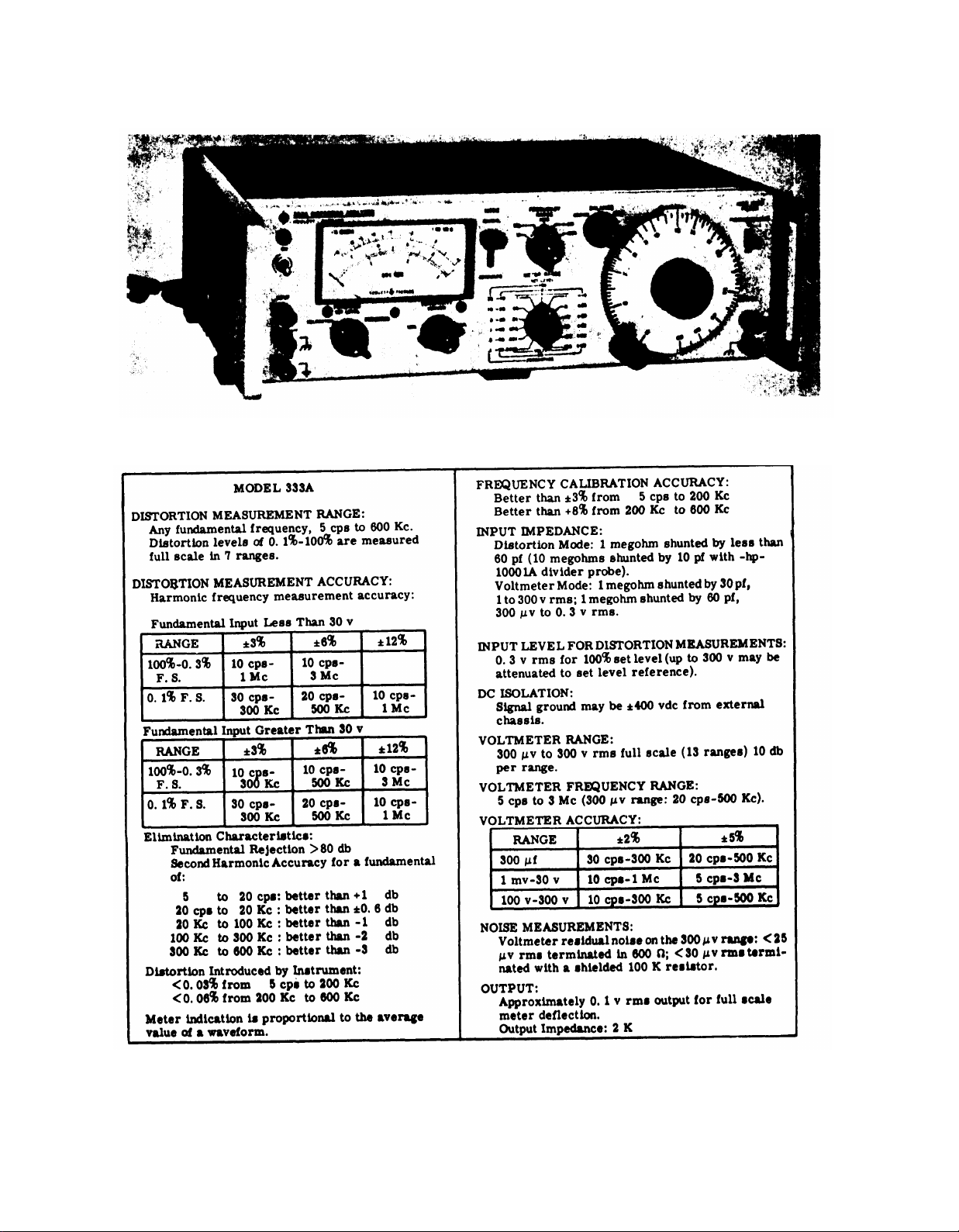
Figure 1-1. Model 333A Distortion Analyzer
Table 1-1. Specifications
1-1
Page 6
TM 11-6625-1576-15
Section I
Table 1-1
Model 333A/334A
Table 1-1. Specifications (Cont ‘d)
1-2
Page 7

TM 11-6625-1576-15
SECTION I
GENERAL INFORMATION
1-A.1 Scope
This manual includes installation and operation instructions and
covers operator’s, organizational, direct support (DS), general support
(GS), and depot maintenance. It describes Hewlett-Packard (Federal support
Code 80537) Distortion Analyzer Models 333A and 334A (fig. l-l). A
basic issue items list for this equipmnent is not included as part of
this manual.
1-A.2 Index of Publications
Refer to the latest issue of DA Pam 310-4 to determine whether there
are new editions, changes, or additional publications pertaining to the
equipment. DA Pam 310-4 is an index of current technical manuals,
technical bulletins, supply manuals (types 7, 8, and 9), supply bulletins,
lubrication orders, and modification work orders that are available through
publications supply channels. The index lists the individual parts (-10,
-20, - 35P, etc) and the latest changes to and revisions of each equipment
publication.
l-A.3 Forms and Records
a. Reports of Maintenance and Unsatisfactory
ment forms and records in accordance with instructions in TM 38-750.
b. Report of Damaged or Improper Shipment. Fill out and forward
DD Form 6 (Report of Damaged or Improper Shipment) as prescribed in
AR 700-58 (Army), NAVSANDA Publication 378 (Navy), and AFR ‘71-4
air Force).
c. Reporting of Equipment Manual Improvements. Report of errors,
omissions, and recommendations for improving this manual by the
individual user is encouraged.
2028 (Recommended Changes to DA Publications) and forwarded direct
to Commanding General, U. S. Army Electronics Command,
ATTN: AMSEL-MR-NMP-AD, Fort Monmouth, New Jersey 07703.
Reports should be submitted on DA Form
Equipment. Use equip-
1-2.1
Page 8

Page 9

TM 11-6625-1576-15
Model 333A/334A
1-1. DESCRIPTION.
1-2. The Hewlett-Packard Models
Distortion Analyzers are solid state
measuring distortion and ac voltages.
333A and 334A include two control loops that automatically tune both legs of a bridge circuit which re -
jects the fundamental when the rejection circuit is
initially set within the range of the loops. A high im pedance detector which operates from 500 Kc to greater
than 65 Mc provides the capability” of monitoring the
distortion of the amplitude modulation on an rf carrier.
1-3. Distortion levels of O. 1% to 1OO% full scale are
measured in seven ranges for any fundamental fre quency of 5 cps to 600 Kc.
to 3Mc. The high sensitivity of these instruments requires only O. 3 v rms for the 100% set level reference.
The distortion characteristics can be monitored at the
OUTPUT connectors with an oscilloscope, a true rms
voltmeter, or a wave analyzer. The instruments are
capable of an isolation voltage of 400 volts above chassis
ground.
1-4. The voltmeter can be used separately for general
purpose voltage and gain measurements. It has a fre quency range of 5 cps to 3 Mc (20 cps to 500 Kc for 300
pv range) and a voltage range of 300 pv to 300 v rms
full scale.
1-5. The AM detector included in the Model 334A is
a broadband dc restoring peak detector consisting of a
semiconductor diode and filter circuit. AM distortion
levels as low as O. 3% can be measured on a 3 v to 8 v
rms carrier modulated 30% in the standard broadcast
Harmonics are indicated up
333A and 334A
instruments for
The Models
Paragraphs l-l to l-13
Section I
band, and lower than 1% distortion can be measured
at the same level of the carrier up to 65 Mc.
1-6. ACCESSORY FEATURES.
1-7. The accessory available with the 333A and 334A
Distortion Analyzers is a voltage divider probe, -hpModel No. 1000lA. The features of the probe are:
a. 10 megohms shunted by 10 pf, giving 10:1
attenuation.
b. DC to 30 Mc bandwidth.
c. 2% division accuracy.
d. 600 v peak input.
e. 5 ns rise-time.
1-8. OPTION.
1-9. Option 0l is a standard -hp- Model 333A or 334A
with a special meter and meter amplifier, compen-
sated to permit response to VU (volume units)
characteristics.
1-11. Modifications
1-12, Specification C10-334A is a standard
334A Distortion Analyzer modified by placing
the INPUT and OUTPUT terminals on the rear
panel of the instrument. The rear terminals
are binding post connectors and are in
parallel with the front panel terminals.
Due to the rear terminal leads, the shunt
capacitance of the instrument is increased
by 20pF .
1-3
Page 10

Page 11

TM 11-6625-1576-15
Model333A/334A
Paragraphs 2-1 to 2-19
SECTION II
INSTALLATION
Section II
2-1. INTRODUCTION.
2-2. This section contains information and instructions necessary for the installation and shipping of the
Models 333A/334A Distortion Analyzers. Included
are initial inspection procedures, power and grounding
requirements,installation information, and instruc tions for repackaging for shipment.
2-3. INSPECTION.
2-4. This instrument was carefully inspected both
mechanically and electrically before shipment. It
should be physically free of mars or scratches and in
perfect electrical order upon receipt. To confirm
this, the instrument should be inspected for physical
damage in transit. Also check for supplied accessories,
and test the electrical performance of the instrument
using the procedure outlined in Paragraph 5-5.
2-5. POWER REQUIREMENTS.
2-6. The Model 333A/334A can be operated from any
ac source of 115 or 230 volts (+10%), at 50- 1000 cps.
With the instrument disconnected from the ac power
source, move the slide (located on the rear panel) un-
til the desired line voltage appears. The instrument
can be battery operated by connecting two 28-50 V
batteries (rated 80 milliamperes) to the battery ter-
minal on the rear panel. Power dissipation is 10 watts
maximum.
2-7. THREE-CONDUCTOR POWER CABLE.
2-8. To protect operating personnel, the National
Electrical Manufacturers’ Association (NEMA) recom-
mends that the instrument panel and cabinet be grounded.
All Hewlett-Packard instruments are equipped with a
three -conductor power cable, which when plugged into an appropriate receptacle, grounds the instrument
The offset pin on the power cable three-prong connec-
tor is the ground wire.
2-9. To preserve the protection feature when operat-
ing the instrument from a two-contact outlet, use a
three-prong to two-prong adapter and connect the
green pigtail on the adapter to ground.
2-10. INSTALLATION.
2-11 The Model 333A/334A is fully transistorized;
therefore, no special cooling is required. However,
the instrument should not be operated where the ambient temperature exceeds 55 C (191 F).
2-12. BENCH INSTALLATION.
2-1% The Model 333A/34A is shipped with plastic
feet and tilt stand in place, ready for use as a bench
instrument.
2-14. RACK INSTALLATION.
2-15. The Model 333A/334A may be rack mounted by
using the 5“ RackMount Kit (-hp- Part No. 5060-0775).
Instructions for the conversion are included with the
The rack mount for the Model 333A/334A is an
kit.
ELA standard width of 19 inches. when mounted in a
rack using the rack mount kit, additional support at
the rear of the instrument should be provided if vibra
tion or similar stress is likely.
2-16. REPACKAGING FOR SHIPMENT.
2-17. The following paragraphs contain a general guide
for repackaging of the instrument for shipment. Refer
to Paragraph 2-18 if the original container is to be
used; 2-19 if it is not.
2-18. If original container is to be used, proceed as
follows:
a. Place instrument in original container if avail-
able.
b. Ensure that container is well sealed with strong
tape or metal bands.
2-19. If original container is not to be used, proceed
as follows:
a. Wrap instrument in heavy paper or plastic be-
fore placing in an inner container.
b. Place packing material around all sides of in-
strument and protect panel face with cardboard strips.
c. Place instrument and inner container in a heavy
carton or wooden box and seal with strong tape or
metal bands.
d. Mark shipping container with “DELICATE
INSTRUMENT," "“RAGILE,” etc.
2-1
Page 12
TM 11-6625-1576-15
Section III
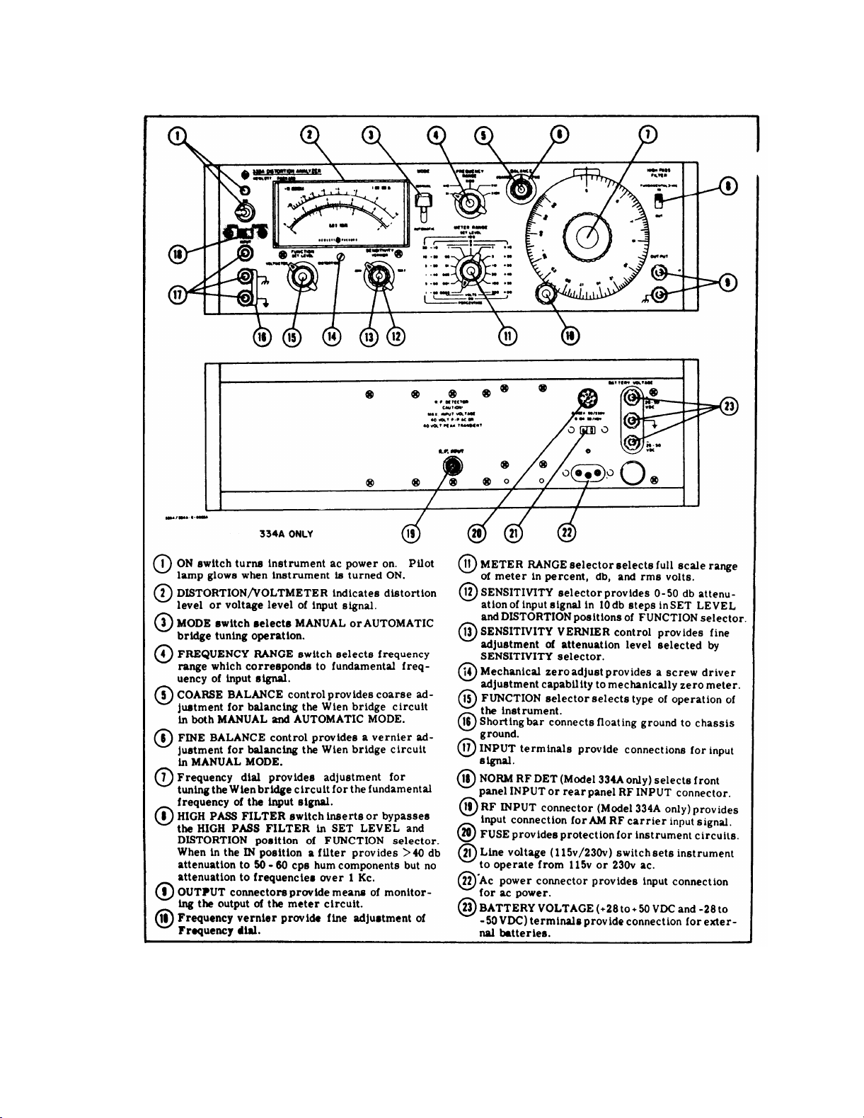
Figure 3-1
Model 333A/334A
3-0
Figure 3-1. Front and Rear Panel Description
Page 13
TM 11-6625-1576-15
Model 333A/334A
Paragraphs-3-l to 3-15
Section III
SECTION III
OPERATING INSTRUCTIONS
3-1. INTRODUCTION.
3-2. The Models 333A and 334A Distortion Analyzers
measure total harmonic distortion from 5 cps to 600
Kc. Harmonics up to 3 Mc are included. The sharp
elimination characteristics, >80 db, the low level of
instrument induced distortion, and the meter accuracy
of the 333A and the 334A result in accurate measurement of low level harmonic content in the input signal.
3-3. An RMS voltmeter is inherent in the 333A and
334A, The voltmeter provides a full scale sensitivity
of 300 u volts rms (residual noise <25 u volts). The
voltmeter frequency range is from 5 cps to 3 Mc except on the 0. 0003 volt range, which is from 20 cps to
500 Kc.
3-4. CONTROLS AND INDICATORS.
3-5. Figure 3-1 illustrates and describes the function
of all front and rear panel controls, connectors, and
indlcators.
keyed to a drawing included within the figure.
3-6. ADJUSTMENTS OF MECHANICAL ZERO.
3-7. The procedure for adjustment of mechanical
zero is given in Section V, Paragraph 5-25.
3-8. GENERAL OPERATING INFORMATION.
3-9. INPUT CONNECTIONS.
3-10. Signal source can be connected to the 333A and
334A through twisted pair leads or a shielded cable
with banana plug connectors. Keep all test leads as
short as possible to avoid extraneous pickup from
stray ac fields,
battery operation is recommended to avoid ground
loops.
by connecting only one instrument in a test setup
directly to power line ground through a NEMA (threeprong) connector,
the power source through a three-prong to two-prong
adapter and leave the pigtail disconnected. Both the
333A and 334A have a dc isolation of ±400 vdc from
the external chassis with the shorting bar, (item 16 ,
Figure 3-1), disconnected.
3-11. VOLTMETER CHARACTERISTICS.
9-12. The RMS VOLTS markings on the meter face are
based on the ratio between the average and effective
(rms) values of a pure sine wave. The ratio of aver-
age to effective values in a true sine wave is approxi-
mately O. 9 to 1.When the meter is used to measure
complex waves,
rms value of the signal applied. This deviation of
meter indication exists because the ratios of average
to effective values are usually not the same in a com plexwave as in a sine wave. The amount of deviation
depends on magnitude and phase relation between
harmonics and fundamental frequency of the signal
The description of each component is
When measuring low-level signals,
Another method for avoiding ground loops is
Connect all other instruments to
the voltage indicated may not be the
applied. Table 3-1 shows the deviation of the meter
indication of a sine wave partly distorted by harmonic..
As indicated in the table, harmonic content of less
than approximately 10% results in very small errors.
Table 3-1
Effect of Harmonics on Voltage Measurements
Input Voltage True
Characteristic
Fundamental = 100
Fundamental +10% 100. s
2nd harmonic
Fundamental +20%
2nd harmonic
Fundamental +50%
2nd harmonic
Fundamental +10%
3rd harmonic
Fundamental +20%
3rd harmonic
Fundamental +50%
3rd harmonic
This chart is universal in application
since time errors are inherent in
all average-responding type voltagemeasuring instruments.
3-13. In distortion measurements where the fundamental frequency is suppressed and the remainder of the
signal is measured, the reading obtained on an average-
responding meter may deviate from the true total rms
value. When residual wave contains many inharmonically related sinusoids, the maximum error in the distortion reading is about 11% low for distorilon levels
below 10%.
Measured Maximum Error Total
Distortion In Meter Indication Distortion
2. 5%
This example represents the maximum possible error,
and in most cases the error is less. In distortion
measurements, the reading of an average-responding
meter is sufficiently close to the rms value to be
satisfactory under most measurement conditions.
3-14. USE OF OUTPUT TERMINALS.
3-15. The OUTPUT terminals provide a O. 1 v rms
output for full scale meter deflection
minals can be used to monitor the output signal with
an oscilloscope,
analyzer. The combination of the distortion meter
and oscilloscope provides more significant information
+0. 11 X O. 025 =
0.00027
RMS Value
100 100
102
112
100.5
102
112
NOTE
a true rms voltmeter, or a wave
Meter
Indication
100
100-102
100-110
96-104
94-108
90-116
0.025 +0. 0027 =
0.0277 or 2.8%
These ter-
3-l
Page 14

TM 11-6625-1576-15
Section III
Paragraphs 3-16 to 3-22
about the device under test than the expression of dis-
tortion magnitude alone.
Information obtained from
the oscilloscope pattern is specific and reveals the
nature of the distortion that sometimes occurs at such
low levels that it is difficult to detect in the presence
of hum and noise.
The impedance at the OUTPUT
terminals is 2000 ohms, therefore, capacitive loads
greater than 50 pf should ‘be avoided to maintain the
accuracy of meter readings.
3-16. OPERATING PROCEDURES.
3-17. The 333A and 334A Distortion Analyzers can be
operated from an ac power source ( 115/230 volt) or a
dc power source (+28 to +50 and -28 to -50 volt source).
If a dc source is used, check the -25 v output. If
necessary, adjust the power supply according to the
procedures in Paragraph 5-27.
3-18. DISTORTION MEASUREMENT.
3- 19. DISTORTION MEASUREMENT IN PERCENT,
AUTOMATIC MODE.
a. Position FUNCTION selector to SET LEVEL.
b. Position MODE switch to MANUAL.
c. If fundamental frequency is 1 Kc or greater,
position HIGH PASS FILTER SWITCH to IN.
d. Rotate SENSITIVITY selector to MIN position.
NOTE
The bandwith of the SENSITIVITY se-
lector is reduced in the two extreme
CCW positions (positions used with an
input signal greater than 30 v).
e. Position METER RANGE selector to SET LEVEL
100%).
f. Connect test leads from device under test to
INPUT terminals.
REMOVE SHORTING STRAP BETWEEN
FLOATING GROUND ~ AND CHASSIS
GROUND (+) TERMINALS ON FRONT
PANEL INPUT TERMINALS WHEN
MEASURING DISTORTION BETWEEN
TWO POINTS WHICH ARE BOTH ABOVE
GROUND POTENTIAL.
g. With SENSITIVITY VERNIER control max. CCW,
position SENSITIVITY selector for meter indication
greater than 1/3 full scale.
NOTE
If unable to adjust for full scale deflection which indicates input signal is be-
low O. 3 volts, use manual mode and
position METER RANGE selector down-
scale. Use this new position as the 100%
SET LEVEL position, thus making the
next range 30%, etc.
h. Adjust SENSITIVITY VENIER control for full
scale deflection.
j. Position FRIQUENCY RANGE selector and
frequency dial to fundamental frequency of input signal.
3-2
Model 333A/334A
k. Position FUNCTION selector to DISTORTION,
m. Adjust METER RANGE selector and frequency
dial vernier control for minimum meter indication.
n. Adjust COARSE and FINE BALANCE controls
for further reduction of meter indication. Meter indication must be less than 10%of SET LEVEL indication.
p. Position MODE switch to AUTOMATIC.
r. Observe percentage of distortion indicated on
meter. Meter indication is in conjunction with METER
RANGE selector. For example, if meter indicates
.4 and METER RANGE selector is on 1% position,
distortion measured is 0.4%.
NOTE
RMS voltage of input signal being analyzed for distortion can be measured
by positioning FUNCTION selector to
VOLTMETER position.
DISTORTION MEASUREMENT IN PERCENT,
3-20.
MANUAL MODE.
NOTE
In MANUAL mode the accuracy of dis tortion measurements is affected by
frequency stability of the input signal.
An inaccuracy in distortion indications
occure when the frequency drift of the input signal exceeds the bandwidth of the
rejection curve.
Perform steps a through n in Paragraph 3-19.
a.
Repeat steps m and n until no further reduction
b.
in meter
-
indication can be obtained.
c. Observe percentage of distortion indicated on
meter.
3-21. DISTORTION MEASUREMENT IN DB,
AUTOMATIC MODE .
a. Perform steps a through g of Paragraph 3-19.
b. Adjust SENSITIVITY VERNIER control for 0 db
meter indication.
c. Perform steps j through 3-19.
d. Observe meter indication for distortion in db.
NOTE
Distortion in db is obtained by algebraically adding meter indication to
db indicated by METER RANGE se-
lector: for example, If meter indicates -2 and METER RANGE selector is on -20 db position, distortion
measured is -22 db.
3-22. DISTORTION MEASUREMENT IN DB, MANUAL
MODE .
NOTE
Notes in Paragraphs 3-20 and 3-21
apply.
a. Perform steps a through g of Paragraph 3-19.
b. Adjust SENSITIVITY VERNIER control for O db
meter indication.
Page 15
Model 333A/334A
c. Perform steps j through n of Paragraph 3-19.
d. Repeat steps m and n until no further reduction
n meter indication can be obtained.
e. Observe meter indication for distortion in db.
3-23. DISTORTION MEASUREMENT OF AM RF
CARRIERS. (334A Only)
a. Set NORM - RF SET selector to RF SET.
OBSERVE MAXIMUM INPUT VOLTAGES
AS INDICATED ON REAR PANEL.
b. Connect Input to RF INPUT on rear panel.
c. Adjust SENSITIVITY VERNIER control for O db
meter indication.
d. Perform steps j through n of Paragraph 3-19.
e. Refer to Paragraph 3-20 for manual measure-
ment in percent.
TM 11-6625-1576-15
Paragraphs 3-23 to 3-27
3-25. The 333A and 334A perform as general purpose
AC Voltmeters when the FUNCTION selector is set
to VOLTMETER position.
NOTE
With the FUNCTION selector in VOLT-
METER position, the SENSITIVITY selector is disabled.
a, Position METER RANGE selector to a range
exceeding the value of the signal to be measured.
b. Connect signal to INPUT terminals.
c. Select a METER RANGE to give a reading as
close to full scale as possible and observe meter
indication.
3-26. OUTPUT TERMINALS.
3-27. In VOLTMETER or SET LEVEL position of
FUNCTION selector, the 333A/334A can be used as a
low distortion, high gain, wideband preamplifier. A
portion of the meter input (O. 1 v RMS output for full
scale meter deflection) is provided at the OUTPUT
terminal J2. In the DISTORTION position, the distor-
tion is provided for monitoring purposes.
Section III
the
f. Refer to Paragraph 3-21 and 3-22 for automatic
and manual measurement in db.
-24. VOLTMETER MODE.
NOTE
If DBM measurements are to be made,
the DB markings on the METER RANGE
switch must each be lowered by 10.
That is, the DB marking for the O. 3 v
range becomes-10 DBM, 1 v range becomes O DBM, 3 v range becomes +10
DBM etc. If the other DB markings are
used, the DBM readings will be 10 DBM
high.
DO NOT EXCEED THE VOLTAGES
LISTED BELOW TO PREVENT BLOWING
FUSE F2:
VOLTMETER.= -1 V RANGE
AND BELOW, AND DISTORTION
ANALYZER, MODE-MAXIMUM
SENSITIVITY.
1. 300 V ABOVE 100 CPS
2. 50 V ABOVE 1 KC
IF LOW FREQUENCIES ARE NOT TO
BE MEASURED, Cl MAY BE REPLACED
WITH A SMALLER CAPACITOR, AND
THE VOLTAGE LIMITS OF F2 MAY BE
RAISED ACCORDINGLY.
3-3
Page 16
TM11-6625-1576-15
Section IV
Figure 4-1
Model 333A/334A
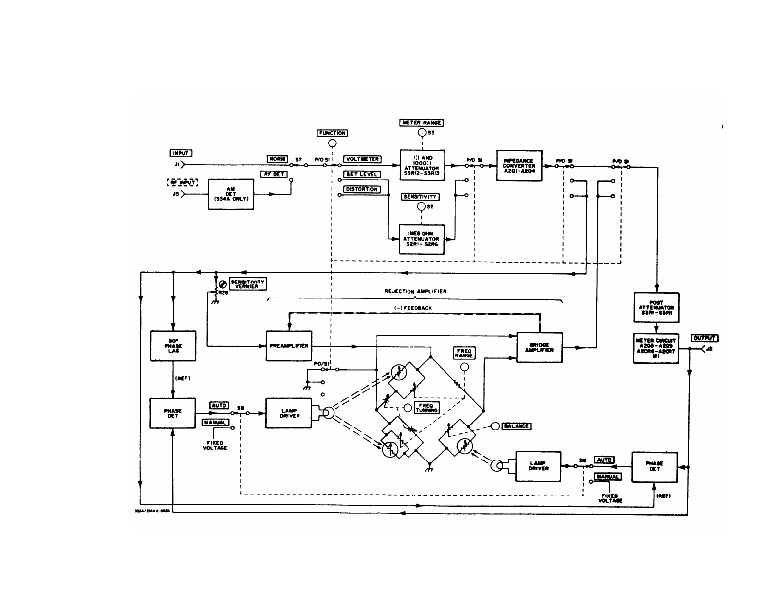
Figure 4-1. Block Diagram
Page 17

TM 11-6625-1576-15
Model 333A/334A
paragraphs 4-1 to 4-12
Section IV
SECTION IV
THEORY OF
4-1. OVERALL DESCRIPTION.
4-2. Models 333A and 334A Distortion Analyzers include an impedance converter, a rejection amplifier,
a metering circuit, and a power supply, The Model
334A also contains an
of the instruments is shown in Figure 4-1. The im pedance converter provides a low noise input circuit
with a high input impedance independent of source
impedance placed at the INPUT terminals. The re-
jection amplifier rejects the fundamental frequency of
an input signal and passes the remaining frequency
components on to the metering circuit for measuring
distortion.
indications of distortion and voltage levels on the front
panel meter, M 1. The AM detector (Model 334A only)
detects the modulating signal from the RF carrier and
filters any RF components from the modulating signal
before it is applied to the impedance converter circuit.
4-3. BLOCK DIAGRAM DESCRIPTION.
4-4. DISTORTION MEASURING OPERATION.
4-5. For distortion measurement, the input signal is
applied to the impedance converter, Assembly A2,
through the FUNCTION selector, S1, and the one megohm attenuator, The one megohm attenuator, a voltage
divider network provides 50 db attenuation in 10 db
steps. The desired level of attenuation is selected by
the SENSITIVITY selector, S2. The impedance converter provides an impedance conversion and unity
gain between the instrument INPUT terminals and the
input of the rejection amplifier. The rejection amplifier consists of a preamplifier, a Wien bridge, and a
bridge amplifier. The SENSITIVITY VERNIER control,
at the input of the preamplifier, provides a set level
signal to obtain a full scale reading on the meter for
any voltage level at the input of the instrument. With
the FUNCTION selector in the SET LEVEL position, a
ground is applied in the Wien bridge circuit to allow
a signal reference level to be set up on the meter.
With the FUNCTION selector in the DISTORTION position, the Wien bridge is used as an interstate coupling
network between the preamplifier and bridge amplifier.
The Wien bridge is tuned and balanced to reject the
fundamental frequency of the applied input signal. Two
automatic control loops consisting of two phase detec tors, lamp drivers, lamps, and photocells provide fine
tuning and balance in the AUTOMATIC MODE. The
remaining frequency components are applied to the
bridge amplifier and are measured as distortion by
the metering circuit.
bridge amplifier to the preamplifier narrows the re-
jection response of the Wien bridge. The output of
the rejection amplifier is applied to the metering cir -
cuit through the post-attenuator. The post-attenuator
is used to limit the input signal level applied to the
metering circuit to 1 mv for full scale deflectlon.
The metering circuit sensitivity is increased to 300
u
V for full scale deflection on the 300 pv range. The
metering circuit provides a visual indication of the
The metering circuit provides visual
AM detector. A block diagram
Negative feedback from the
OPERATION
distortion level of the input signal. In addition to the
visual indication provided by the meter, the OUTPUT
terminals provide a means of monitoring the distortion
components.
4-6. DISTORTION MEASUREMENT IN AM
CARRIERS.
4-7. The Model 334A Distortion Analyzer contains an
AM detector circuit for measuring envelope distortion
in AM carriers.The input signal is applied to the input of the AM detector circuit where the modulating
signal is recovered from the RF carrier. The signal
is then applied to the impedance converter circuit
through the one megohm attenuator and then through
the same circuits previously described in the distortion measuring mode operation.
4-8. VOLTMETER OPERATION.
4-9. In the voltmeter mode of operation, the input
signal is applied to the impedance converter circuit
through the 1:1 and 1000:1 attenuator. The 1:1 atten-
uation ratio is used in the .0003 to .3 VOLTS position
of the METER RANGE selector S3, and the 1000:1
attenuation ratio is used in the 1 to 300 VOLTS posit ions.
METER position, the output of the impedance converter
bypasses the rejection amplifier and is applied to the
metering circuit through the post-attenuator (METER
RANGE selector).Metering circuit sensitivity is in-
creased from 1 mv for full scale deflection to 300 uv
on the 300
suring operation.The function of the post-attenuator
and metering circuit is the same for voltmeter opera-
tion as for the distortion measuring operation.
4-11. IMPEDANCE CONVERTER CIRCUIT.
4-12. The input signal to the distortion analyzer is
applied to the impedance converter circuit (refer to
Figure 6-2) through the 1:1 and 1000:1 attenuator
S3R12 in the voltmeter mode of operation and through
the one megohm attenuator S2R1 through S2R6 in the
distortion mode of operation. Capacitive dividers
S2C10 through S2C 10 in the attenuator keep the frequency
response flat.
distortion, high input impedance amplifier circuit
wit h gain independent of the source impedance placed
at the INPUT terminals. Instrument induced distortion of the signal being measured is minimized by
keeping the input impedance and the gain of the impedance converter linear. The input impedance is kept
linear by use of local positive feedback from the source
of A2Ql to the gate of A2Q1 and to the protective diodes
A2CR2 and A2CR3. Thus signals with large source
impedance can be measured accurately. Overall induced distortion is further minimized by a high open
loop gain and 100% negative feedback. The high open
loop gain is achieved by local positive feedback from
With the FUNCTION selector in the VOLT-
uv range, as it was in the distortion mea-
4-10. SCHEMATIC THEORY.
The impedance converter is a low
4-1
Page 18

TM11-6625-1576-15
Section IV
Paragraphs 4-13 to 4-25 and Figure 4-2
the emitter of A2Q3 to the collector of A2Q2. Overall
negative feedback from the emitter circuit of A2Q4 to
the source of A2Q1 results in unity gain from the impedance converter.
4-13. The bias points of the transistors in the impedance converter are selected to minimize instrument
induced distortion. A2Q 1, an extremely low noise,
high impedance field effect transistor, is the major
component that makes linearity of the Impedance converter independent of the signal source impedance.
4-14. REJECTION AMPLIFIER CIRCUIT.
4-15. The rejection amplifier circuit (see Figures 6-3
and 6-6) consists of the preamplifier (A3Q1) thru A3Q3),
the Wien bridge resistive leg and auto control loop
(A5Q1 thru A5Q9 with associated lamp and photocell),
the reactive leg and auto control loop (A5Q10 thru
A5Q 18 with associated lamp and photocell), and the
bridge amplifier (A3Q4 thru A3Q6).
4-16. PREAMPLIFIER CIRCUIT.
4-17. The signal from the impedance converter is ap-
plied to the preamplifier, which is used during SET
LEVEL and DISTORTION measuring operations. Negative feedback from the junction of A3R1O and A3R11 is
applied to the junction of A3R2 and A3C2 to establish
the operating point for A3Q1. Negative feedback from
the emitter of A3Q3 is applied to the emitter of A3Q1
to stabilize the preamplifier. The preamplifier, like
the impedance converter, is designed for high open
loop gain and low closed loop gain to minimize instru-
ment induced distortion.
4-18. WIEN BRIDGE CIRCUIT.
4-19. In the distortion measuring operation the Wien
bridge circuit is used as a rejection filter for the
fundamental frequency of the input signal. With the
FUNCTION selector, S1, in the DISTORTION position,
the Wien bridge is connected as an interstage coupling
network between the preamplifier circuit and the bridge
amplifier circuit. The bridge is tuned to the fundamen-
tal frequency of the input signal by setting the FREQUENCY RANGE selector, S4, for the applicable frequency range, and tuning the capacitors C4A through
C4D. The bridge circuit is balanced by adjusting the
COARSE balance control, R4, and the FINE balance
control, R5.
In the AUTOMATIC MODE fine tuning
and balancing are accomplished by photoelectric cells
which are in the resistive and reactive legs of the
Wien bridge. The error signals for driving the photo-
cells are derived by detecting the bridge output using
the input signal as a reference.
4-20. When the Wien bridge is not tuned exactly to the
frequency to be nulled, a portion of the fundamental
frequency will appear at the bridge output. The phase
of this signal depends on which leg of the bridge is not
tuned, or on the relative errors in tuning if neither is
set correctly. The magnitude of the signal is proportional to the magnitude of the tuning error of either or
both legs of the bridge.
4-2
Model 333A/334A
Figure 4-2. Bridge Waveforms
4-21. Figure 4-2a is a sinusoid input to the Wien bridge.
If the resistive leg of the bridge i
S slightly unbalanced,
the output of the bridge is very small, but has the
waveform shown in Figure 4-2b and is in phase with
the input.
approaches zero
larger, but 180° out of phase, if the null position is
passed.
As the resistive leg is tuned, the signal
amplitude at null and then becomes
When the resistive leg is correctly tuned
and the reactive leg is tuned through null, a similar
waveform is produced, Figure 4-2c. The only difference is that the reactive signal is 90° out of phase with
the resistive signal.
4-22. When the bridge output is detected using the
input signal as the reference, the error signals in
phase or 180° out of phase with the reference develop
a voltage which is used to vary the resistance in the
resistive leg of the bridge, to tune it to the correct
null position, Signals of the form in Figure 4-2c do
not develop any voltage as the resistive detector is
insensitive to input differing from the reference by 90° .
4-23. In an independent, but similar control loop, the
bridge input signal is shifted 90° and used as the
reference signal for the detector. This detector
develops control voltages to null the reactive leg of
the bridge, but is insensitive to signals of the form
in Figure 4-2b which are caused by small tuning
errors of the resistive branch.
4-24. The result is that the two control loops derive
information from a common source and develop two
independent control signals for nulling the two legs
of the bridge. These control voltages are used to
vary the brilliance of lamps, which in turn causes
resistance changes in photocells which form part of
the Wien bridge.
4-25. Refer to Figure 4-3 for the phase relationship
of the bridge error signal and reference voltage at the
base of A5Q4. The shaded portions of the error signals (b and c) indicate that part of the error signal
which contributes to the dc lamp control voltage. As
indicated in d, any error signal that is 90° out of
phase with the reference does not affect the dc lamp
control voltage.
Page 19

Model 333A/334A
4-26. The operation of the reactive branch control loop
is similar to that of the resistive branch. The phase
delay circuit (Figure 6-6), A5Q15, A5Q16, S4AF and
S4C1 through S4C5, shifts the reference voltage 90º,
as shown in Figure 4-3f.
A5Q12 sensitive to components of the bridge error
signal that are 90° out of phase (g and h). The output
of the lamp driver, Q14, controls the brilliance of
A6DS2, which varies the resistance of A6V2 through
A6V5 to tune the branches of the reactive leg. Deck
AR of the FREQUENCY RANGE switch, S4, switches
A5R56 in parallel with A5R55 on the top three frequency
ranges.
A6DS2 will become brighter, and lower the
This makes the detector
TM 11-6625-1576-15
Section IV
Paragraphs 4-26 to 4-27 and Figure 4-3
resistance of A6V2 through A6V5, making variation
in resistance less than on the two lower ranges.
However, less variation in resistance is needed to
tune the leg, because the impedance in the reactive leg
becomes progressively less as the higher frequency
ranges are selected.
4-27. Any error signal that is not an integral multiple
of 90 is the result of the reactive leg of the bridge
being detuned, and the resistive leg being unbalanced.
For example, an error signal that is 45º out of phase
(Figure 4-3e and j) will result in outputs from both
detectors to tune the bridge and reject the fundamental.
.
Figure 4-3. Reference and Error Phase Relationship
4-3
Page 20

TM 11-6625-1576-15
Section IV
Paragraphs 4-28 to 4-35 and Figures 4-4 to 4-5
Figure 4-4. Wien Bridge Circuit and Rejection Characteristics
4-28. When the bridge circuit is tuned and balanced,
the voltage and phase of the fundamental, which appears
at junction of the series reactive leg (S4R1, 3, 5, 7,
or 9 and C4A/B) and the shunt reactive leg (S4R11,
13, 15, 17, or 19, and C4C/D), is the same as at the
midpoint of the resistive leg (A3R12 and A3R14). When
these two voltages are equal and in phase, the funda-
mental frequency will not appear at the drain of the
field effect transistor A3Q4. For frequencies other
than the fundamental,the reactive leg of the Wien
bridge offers various degrees of attenuation and phase
shift which cause a voltage at the output points of the
bridge. This difference voltage between the reactive
leg and resistive leg is amplified by A3Q4, A3Q5, and
A3Q6.
circuit and the rejection characteristics for it.
Figure 4-4 illustrates a typical Wien bridge
positive half of the signal will be passed, and if it is
out of phase, the negative half will be passed.
4-32. The normal working voltage at TP3 is between
0 and -1 volt. The dc output of the filter network
causes the voltage at TP3 to go in a positive direction
(toward zero) for in phase error signals, and in a
negative direction (toward
signals. The change in base voltage is then amplified
by A5Q5 and lamp driver A5Q6. This will change the
brilliance of lamp A6DS1, which will vary the resistance of A6V1 in the direction necessary to balance
the resistive leg of the bridge.
-1 v) for out of phase error
4-29. The Wien bridge circuit is designed to cover a
continuous frequency range of over a decade for each
position of the FREQUENCY RANGE selector, S4. S4
provides course tuning of the reactive leg by changing
the bridge circuit constants in five steps at 1 decade
per step. For the automatic control loop, the reference
voltage is taken from R6 at the input to the rejection
amplifier and applied to the buffer amplifier A5Q7.
The reference voltage is amplified and clipped by A5Q8
and A5Q9 and coupled to the detector A5Q4. The output
of the metering circuit, which contains the fundamental
frequency if either leg of the bridge is untuned, is ap-
plied to the buffer amplifier A5Q1. It is amplified by
A5Q2 and A5Q3 and coupled to the detector A5Q4.
4-30. Refer to Figure 4-5 simplified partial schematic
for detector operation.
to both resistive and reactive detector circuits.
4-31. The signals from the error amplifier, (A5Q2
and A5Q3) will be equal and of opposite phase, and will
cancel out each other when the detector, A5Q4 is off.
However,
square wave gates A5Q4 on, the signal from the col-
lector of A5Q3 will be shorted to ground. Thus the
signal from the collector of A5Q2 will be coupled
through the filter network to the base of AQ5. If the
signal from A5Q2 is in phase with the reference, the
when the positive half of the reference
The discussion is applicable
4-4
Figure 4-5. Auto Control Loop Detector
4-33. When the FUNCTION selector is set to the VOLT-
METER or SET LEVEL position, the junction of the
series and shunt reactive branches of the Wien bridge
is connected to circuit ground through R19 by S1BF
which disables the frequency rejection characteristic
of the bridge circuit. With the bridge circuit disabled,
the rejection amplifier circuit provides one db of gain
for the fundamental frequency and the harmonics. In
the SET LEVEL operation, this signal is used to establish the SET LEVEL reference.
4-34. BRIDGE AMPLIFIER CIRCUIT.
4-35. The bridge amplifier circuit consists of three
stages of amplification, A3Q4 through A3Q6. The
Page 21

TM 11-6625-1576-15
Figure 4-6. Rejection Amplifier Block Diagram and Typical Frequency Rejection Characteristic
first stage of amplification, A3Q4, is a field effect
transistor which amplifies the difference signal between
the gate and the source.
The field effect transistor
is selected for maximum noise performance with the
high impedances of the Wien bridge circuit. The signal
from the drain is applied to the two stage feedback amplifier A3Q5 and A3Q6. The output of A3Q6 is coupled
to the meter circuit by the post attenuator S3R1 through
S3R11. Negative feedback from the output of the bridge
amplifier is applied to the preamplifier circuit to narrow the frequency rejection characteristic. It can be
noted from the rejection characteristic (refer to Figure
4-4) for the bridge that the rejection of harmonic voltages is not constant.
Typically the second harmonic
is attenuated several db more than the third harmonic
and the third more than the fourth. The result of the
negative feedback is illustrated by the rejection charac-
teristic shown in dashed lines on the attenuation and
phase characteristic of Figure 4-4. Figure 4-6 shows
a simplified block diagram of the rejection amplifier
with the typical frequency-rejection characteristic.
Refer to Figure 4-7, Bandwidth Versus Null Depth for
further detail on the rejection characteristic.
4-36. HIGH PASS FILTER.
4-37. The HIGH PASS FILTER (see Figure 6-3) is
normally used when the fundamental of the input signal
is greater than 1 Kc.
In the voltmeter mode of operation, the filter is not used. In the SET LEVEL and
DISTORTION position of the FUNCTION switch the
filter presents >50 db attenuation to 50 or 60 cycle
hum components, but offers no attenuation to frequencies over 1 Kc.
The filter assembly, A7, consists of
A7C1, A7C2, and A7L1. The filter can be inserted
or bypassed by the HIGH PASS FILTER switch, S9.
4-38. METER CIRCUIT.
4-39. The meter circuit (refer to Figure 6-4) consists
of the post attenuator,
the meter amplifier circuit,
and the meter rectifier circuit.
4-40. POST ATTENUATOR.
4-41. The post attenuator, S3R1 through S3R11, is a
series of resistive networks which attenuate the input
signal in 10 db steps.
The attenuator is used in con-
junction with either the input sensitivity attenuator or
the 1000:1 attenuator to limit the signal level to the
meter amplifier to 1 mv for full scale deflection on
all ranges from 1 mv to 300 v full scale. The meter
circuit sensitivity is increased to 300 uv for full scale
deflection on the 300
V range by switching resistors
u
A2R29 and A2R30 into the calibration network. Resistor A2R41 and capacitor A2C29 are also switched into
Paragraphs 4-36 to 4-45 and Figure 4-6
Section IV
the calibration network on the 300
Pv range to extend
the passband of the amplifier.
4-42. METER AMPLIFIER CIRCUIT.
4-43. The meter amplifier circuit consists of a five
stage amplifier circuit,
A2Q5 through A2Q9, which
develops the current for full scale meter deflection.
Negative dc feedback from the emitter circuit of
A2Q8 is applied to the base of A2Q5 to stabilize the
dc operating point of the meter amplifier circuit and
to minimize the tendency for dc drift due to ambient
temperature changes.
A2R51 and A3CR8 are electric-
ally in the circuit only when the meter circuit is over-
loaded. When the voltage on the emitter of A2Q9 becomes abnormally large during an overload, A2CR8
breaks down and provides a lower resistance charging
path for A2C15 which reduces the transient recovery
time of the meter circuit.
Negative ac feedback is
applied from the collector circuit of A2Q9 to the emitter circuit of A2Q5. This feedback is used to ensure
flat frequency response, to improve linearity, and to
reduce the effect of variation of transistor parameters
with environmental changes.
In this manner, the
calibration of the instrument is made dependent on
high quality passive components.
4-44, METER RECTIFIER CIRCUIT.
4-45. The meter rectifier is connected in a bridge type
of configuration with a diode in each upper branch and
a dc milliammeter connected across the midpoints of
the bridge.
strated in Figure 4-8.
The simplified meter rectifier is illu-
The generator represented by
A2Q5 through A2Q9 with the internal impedance R
provides the meter,
M1, with current for full scale
deflection and develops a voltage across the calibration
network which closes the ac feedback loop. Capacitors
A2C27 and A2C28 are used as coupling capacitors for
the ac feedback loop, output signal to the OUTPUT
connector, and the bridge error signal to the input of
the automatic fine tuning loops. The mechanical inertia
of the meter and A2C26 prevents the meter from re-
sponding to individual current pulses.
Therefore,
the meter indication corresponds to the average value
of the current pulses rather than the peak value. The
meter is calibrated to indicate the rms value of a sine
wave. Resistor A2R45 impresses a fixed bias across
diodes A2CR6 and A2CR7 (biasing them close to the
barrier voltage) to make the meter circuit response
linear to large variations in signal amplitude. The
linearity of this type of circuit is also increased by
including the meter circuit in the overall feedback
loop.
4-5
O
Page 22

TM 11-6625-1576-15
Section IV
Figure 4-7
Model 333A/334A
4-6
Figure 4-7. Bandwidth Versus Null Depth
Page 23

TM 11-6625-1576-15
model
333A/334A
Paragraphs 4-46 to 4-52 and Figure 4-8
Section IV
Figure 4-8. Simplified Metering Circuit
4-46. POWER SUPPLY CIRCUIT.
4-47. The power supply circuit (refer to Figure 6-5)
consists of a +25 voIt series regulated supply and a
-25 volt series regulated supply which is the reference
supply for the +25 volt supply.
4-48. The -25 volt regulated supply is of the conventional series regulator type. The amplifier A1Q5 is
used to increase the loop gain of the circuit, thus improving voltage regulation. The positive feedback ap-
plied to the junction of A1R1l and A1R12 is used to
further improve the line frequency suppression of the
circuit.
4-49. The +25 volt regulated supply is of the conventional series regulator type and operates the same as
the -25 volt regulated supply.
4-50. Diodes A1CR5 and A1CR6 are coupling and pro-
tection diodes for external battery supplies. The diodes
protect the series regulator circuits from application
of incorrect polarity at the battery input terminals.
The diodes also protect external batteries from being
charged when the ac power is being used with batteries
connected to the battery terminals.
4-51. RF
4-52. The RF detector circuit consists of a rectifier
A4CR1 and filter circuit shown on the schematic diagram of Figure 6-2. The RF signal is applied to the
circuit through the RF INPUT connector on the rear
panel. The rectifier diode A4CR1 recovers the modulating signal from the RF carrier and the filter circuit
removes any RF components before the signal is ap pIied to the impedance converter circuit through the
NORM -RF DET switch, S7.
DETECTOR CIRCUIT. (334A only)
4-7
Page 24

TM 11-6625-1576-15
Section V
Table 5-1
Model 333A/334A
Table 5-1. Test Equipment Required
5-0
Page 25

Model 333A/334A
SECTION V
MAINTENANCE
TM 11-6625-1576-15
Paragraphs 5-l to 5-9 and Figure 5-1
Section V
5-1. INTRODUCTION.
5-2. This section contains maintenance and service
information for the 333A and 334A Distortion Analyz -
Included are Performance Checks, Adjustment
ers.
and Calibration Procedures, and Troubleshooting
Techniques.
5-3. TEST EQUIPMENT REQUIRED.
5-4. Test equipment used in the calibration of the 333A
and 334A is given in Table 5-1, Test Equipment Re-
quired.
used,
commercially available test equipment.
5-5. PERFORMANCE CHECKS.
5-6. The Performance Checks are in-cabinet procedures that can be used to verify instrument performance,
maintenance, to check specifications after a repair,
or for incoming quality control inspection.
5-7. Performance Checks for both the 333A and 334A
are provided. The performance checks are applicable
to both instruments except where noted in paragraph
heading.
5-8. The Performance Checks are performed with the
ac power cord connected to nominal line voltage (115
v/230 V) 50 to 1000 cps, MODE SWITCH to MANUAL,
HIGH PASS FILTER to OUT, and NORM RF DET switch
to NORM, unless otherwise specified. Selector positions for the SENSITIVITY Selector will be referred
to as follows: MIN=Position 1, next step-Position 2,
etc, to Max= Position 6.
5-9.
Set
This table lists the type of equipment to be
required characteristics, and recommended
These procedures can be used for periodic
FUNDAMENTAL REJECTION CHECK
a.
Connect 33lA/332A as shown in Figure 5-1.
b.
Set Distortion Analyzer controls as follows:
FUNCTION Selector . . . . . . VOLTMETER
METER RANGE Selector . . . . . . . 1 VOLT
FREQUENCY RANGE Selector . . . . . . X1OO
Frequency Dial . . . . . . . . . . . . . . . 50
filter (White Instr Lab Model
2640)
. . . . . . . . . . . . . . . . .. . . . . . . .5Kc
to 5 K
on Distortion Analyzer meter.
LEVEL. Switch METER RANGE to O. 3 VOLTS. Adjust
SENSITIVITY controls for full scale meter indication.
as follows:
for maximum meter reading (approximately 1 Kc).
meter indication.
TORTION. Adjust BALANCE controls and FREQUENCY dial for null indication on Distortion Analyzer
meter. Reduce Distortion Analyzer METER RANGE
selector setting as necessary to maintain deflection
on meter scale.
Analyzer meter,
continue to adjust for a null indication. Reduce Wave
Analyzer RANGE setting as necessary to maintain
deflection on meter scale.
c. Set Test Oscillator (-hp - Model 651A) frequencv
C and adjust amplitude for indication of 1.0 volt
d. Switch Distortion Analyzer FUNCTION to SET
e. Set Wave Analyzer controls (-hp - Model 302A)
SCALE VALUE . . . . . . . . . . RELATIVE
MAX INPUT VOLTAGE . . . . . . . . ...1
RANGE . . . . . . . . . . . . . . 0 DECIBELS
MODE SELECTOR . . . . . . . . . .NORMAL
f. Adjust Wave Analyzer FREQUENCY controls
g. Adjust Wave Analyzer REF ADJUST for O db
NOTE
If the range of the REF ADJUST control
is insufficient to set meter to O db reference,adjust the Distortion Analyzer
SENSITIVITY VERNIER control slightly
to set reference.
Switch Distortion Analyzer FUNCTION to DIS-
h.
j. After achieving null indication on Distortion
The Distortion Analyzer OUTPUT is a O
to O. 1 volt signal representing a percent-
age of full scale,
observe Wave Analyzer mete r and
NOTE
regardless of RANGE
Figure 5-1. Test Setup for Fundamental Rejection Check
5-1
Page 26

TM 11-6625-1576-15
Section V
Paragraphs 5-10 to 5-11, Figure 5-2 and Table 5-2
setting.
switch represents 10 db fundamental rejection. Therefore, the total fundamental
rejection is the sum of the Wave Analyzer
reading and the 333A/334A indication.
k. The Distortion Analyzer METER RANGE setting
plus the Wave Analyzer RANGE setting plus the two
meter indications shall total more than -80 db.
5-10. SECOND HARMONIC ACCURACY CHECK.
a. Connect Test Oscillator (-hp-Model 651A) 600Ω
output to Distortion Analyzer *
b. Set Distortion Analyzer controls as follows:
FUNCTION Selector . . . . . . . SET LEVEL
FREQUENCY RANGE . . . . . . . . . . . X1
Frequency Dial . . . . . . . . . . . . . . .20
METER RANGE Selector . . . . . . . . . 0 DB
c. Set Test Oscillator controls (-hp- Model 651A)
as follows:
FREQUENCY RANGE . . . . . . . . . . . X10
FREQUENCY Dial. . . . . . . . . . . . . 2
OUTPUT ATTENUATOR . . . . . 1.0 VOLTS
AMPLITUDE . . . . . . . . . . . . . . l Volt
d. Adjust Distortion Analyzer SENSITIVITY controls for a meter reading of O db.
e. Switch Distortion Analyzer FUNCTION selector
to DISTORTION. Adjust Frequency dial and BALANCE
controls for a null indication on meter.
f. Switch Distortion Analyzer FUNCTION selector
to SET LEVEL.
g. Adjust Test Oscillator frequency to 40 cps. Adjust AMPLITUDE control for a O db indication on the
Distortion Analyzer meter.
h. Switch Distortion Analyzer FUNCTION selector
to DISTORTION. The meter reading shall not change
more than ±0. 6 db.
Each decrease of the RANGE
Model 333A/334A
j. Repeat steps a through h at the frequency settings
indicated in Table 5-2.
change within the limits specified.
Table 5-2. Second Harmonic Accuracy Check
5-11.
DISTORTION INTRODUCED BY INSTRUMENT
CHECK AND AUTOMATIC CONTROL LOOP
OPERATION.
Connect 333A/334A as shown in Figure 5-2.
a.
Set Distortion Analyzer controls as follows:
b.
FUNCTION Selector . . . . . . . SET LEVEL
SENSITIVITY Selector
SENSITIVITY VERNIER Control . . full CCW
METER RANGE Selector . . . . . . . . . . 0 db
FREQUENCY RANGE Selector . . . . . . . Xl
Frequency Dial . . . . . . . . . . . . . . .5
Set oscillator for approximately 1 volt output at
c.
5 cycles.
d. Set filter box for 5 cycles.
e. Adjust oscillator amplitude for an indication of
+2 db on the Distortion Analyzer meter.
f. Switch Distortion Analyzer FUNCTION selector
to DISTORTION. Adjust frequency dial and BALANCE
controls for a null meter indication.
lower 1/3 of meter scale, decrease METER RANGE
selector setting. )
g. The meter indication at “null” shall be at least
-8 db on the -60 db METER RANGE which is equiva-
lent to -70 db. Note reading.
The meter readings shall
. Position 1 step CCW
from Full CW position
(If reading is in
5-2
Figure 5-2. Instrument Induced Distorition and Automatic Control Loop Test Setup
Page 27

Model 333A/334A
TM 11-6625-1576-15
Section V
Paragraph 5-12, Table 5-3, and Figure 5-3
h. Set METER RANGE to O. 01 volt RANGE and off-
set frequency dial to a lower reading so that meter
cads full scale.
id note distortion level. Distortion level should be
within +3 -O db of manually nulled reading.
j. Set MODE switch to MANUAL (and meter range
to o. 01).
dial reading so that meter reads full scale. Return
MODE switch to automatic. Distortion reading should
be within +3 -O db of manually nulled reading obtained
in step g of this paragraph.
k. Set MODE switch to MANUAL and adjust fre quency dial for null.
trol CW with METER RANGE set at 0. 01 so that meter
reads full scale. Return MODE Switch to AUTOMATIC.
Distortion reading should be within +3 -0 db of manually
nulled reading obtained in step g of this paragraph.
m. Set MODE switch to MANUAL and METER
RANGE to O. 01.
CCW so that meter reads +2 db. Set Mode switch to
Automatic. Distortion reading should be within +3 -O
of manually nulled reading obtained in step g of
this paragraph.
n. Repeat steps b through m with controls set as
indicated in Table 5-3. Except in steps j thru m use
METER RANGE setting of O. 03 to obtain +2 db reading
when detuning Frequency Dial and COARSE BALANCE
Control to verify automatic control loop operation.
Table 5-3. Distortion Introduced By Instrument Check
5-12. FREQUENCY CALIBRATION ACCURACY
a. Connect 333A/334A as shown in Figure 5-3.
Offset frequency dial past null to a higher
CHECK.
Set MODE switch to AUTOMATIC
Adjust COURSE BALANCE Con-
Adjust COARSE BALANCE Control
NOTE
From 5 cps to 10 cps the FREQUENCY
dial may be as much as 3% low. In this
test the dial is held constant, and the input frequency is varied and monitored.
If the dial is low, the input frequency at
null will be high.
put frequency is measured, it will be low
when the dial is low.
Kc the dial may be as much as 8% high,
Consequently, a low frequency reading at
null would indicate that the dial is reading
high.
b.
Set Distortion Analyzer controls as follows:
FUNCTION Selector . . . . . . . SET LEVEL
METER RANGE Selector . . . . . . . . 0 DB
SENSITIVITY Selector . . . . . . . . . . MIN.
FREQUENCY RANGE Selector . . . . . .Xl
Frequency Dial . . . . . . . . . . . . . . . .5
Set Test Oscillator controls (-hp- Model 203A)
c.
as follows:
FREQUENCY RANGE . . . . . . . . . . . X1
FREQUENCY DIAL . . . . . . . . . . . . . . 5
OUTPUT ATTENUATOR . . . . . . 1.0 VOLT
d. Set Electronic Counter controls (-hp - Model
5532A) as follows:
SENSITIVITY . . . . . . . . . . 3 VOLTS RMS
Function Switch. . . . .
DISPLAY . . . . . . . . . . . . . . Fu1l CCW
e. Adjust Test Oscillator AMPLITUDE control for
a full scale indication on the Distortion Analyzer meter.
f. Switch Distortion Analyzer FUNCTION selector
to DISTORTION.
g. Adjust Test Oscillator FREQUENCY DIAL for
a null indication on the Distortion Analyzer meter.
(If reading is in lower 1/3 of meter scale, decrease
METER RANGE selector setting, )
h. Adjust Distortion Analyzer BALANCE controls
for a null indication on the meter. Repeat steps g and
h until a null is reached.
If the period of the in-
From 200 Kc to 600
1 PERIOD AVERAGED
Figure 5.-3. Test Setup for Frequency Calibration Accuracy Check
5-3
Page 28

TM11-6625-1576-15
Section v
Paragraphs 5-13 to 5-16 and Table 5-4
j. The Electronic Counter shall indicate the period
of 5 cps -3%, i. e. 194 to 200 msec.
k. Repeat steps b through h with controls set as
indicated in Table 5-4. The Electronic Counter shall
indicate the Test Oscillator output frequencies within
the limits indicated.
5-13. INPUT RESISTANCE CHECK
a. Connect Test Oscillator (-hp- Model 651A) 600
Ω output to Distortion Analyzer INPUT terminals.
b. Set Distortion Analyzer controls as follows:
FUNCTION Selector . . . . . . VOLTMETER
SENSITIVITY Selector . . . . . . . . . MAX.
SENSITIVITY VERNIER Control . . . . . MIN.
METER RANGE Selector. . . . . . . 1 VOLT
c. Set Test Oscillator controls as follows:
FREQUENCY RANGE . . . . . . . . . . X10
FREQUENCY Dial . . . . . . . . . . . . . 10
OUTPUT ATTENUATOR . . . . . . 1.0 VOLT
d. Adjust Test Oscillator AMPLITUDE control for
an indication of 1.0 volt (E
Analyzer meter.
e. Connect a 100 K
carbon film resistor in series with the Distortion
) rms on the Distortion
in
Ω (R
) ±1. 0%, 1/2 watt, fixed
a
Analyzer INPUT. Note the Distortion Analyzer meter
reading (E
).
o
f. Calculate the Distortion Analyzer input resistance using the following formula:
Model 333A/334A
e. Set Distortion Analyzer controls as follows:
.
FUNCTION Selector . . . . . .DISTORTION
SENSITIVITY Selector . . . . . . . . . . MIN.
METER RANGE Selector . . . . . . . VOLTS
f. Measure Capacitance at each SENSITIVITY
selector setting of the Distortion Analyzer. The L - C
meter shall indicate less than 60 pf on each of these
settings.
5-15. MINIMUM INPUT LEVEL CHECK.
a. Connect Test Oscillator (-hp- Model 651A) 600
Ω output to Distortion Analyzer INPUT terminals l
Terminate test oscillator with
Ω ±1% 1/2 w resistor.
600
Set Distortion Analyzer controls as follows:
b.
FUNCTION Selector . . . . . . . VOLTMETER
METER RANGE Selector . . . . . . .3 VOLT
SENSITIVITY Selector . . . . . . . . . MIN.
SENSITIVITY VERNIER . . . . . . . . , CCW
Set Test Oscillator for 20 cps.
c.
d.
Adjust Test Oscillator amplitude for a Distortion
-
Analyzer
meter indication O. 3 volts.
e. Switch Distortion Analyzer FUNCTION selector
to SET LEVEL.
f. Switch SENSITIVITY selector to MAX and
VERNIER to full CW. The SENSITIVITY controls shall
have sufficient range to give a full scale meter reading.
g. The input resistance shall be 1 M
Ω ±5%.
h. Switch FUNCTION selector to Distortion and
calculate the input resistance in this position. It shall
be 1 M
Ω ±5%.
INPUT SHUNT CAPACITANCE CHECK.
5-14.
Set Distortion Analyzer controls as follows:
a.
FUNCTION Selector . . . . . . . VOLTMETER
METER RANGE Selector . . . . . . . 1 VOLT
Connect an L - C meter to the 333A/334A and
b.
measure the input capacitance.
c. The L - C meter shall indicate less than 30 pf.
d. Switch the Distortion Analyzer on the 0. 3 range
and measure capacitance. Meter shall indicate less
than 60 pf.
5-4
DC ISOLATION CHECK.
5-16.
Connect 333A/334A as shown in Figure 5-4.
a.
REMOVE SHORTING BARS BETWEEN
POWER LINE GROUND TERMINALS ON
DISTORTION ANALYZER INPUT TERMINALS AND FUNCTION GENERATOR OUTPUT TERMINALS.
b.
Set Distortion Analyzer controls as follows:
FUNCTION Selector . . . . . .VOLTMETER
METER RANGE Selector . . . . . . . 1 VOLT
c. Apply ac power to dc power supply and set for
400 v. Set Power SuppIy controls but do not apply dc
to the Distortion Analyzer.
d. Set Function Generator for 1 Kc and adjust the
amplitude control for an indication of 0. 9 on the Distortion Analyzer meter.
Page 29

TM 11-6625-1576-15
Model 333A/334A
Figure 5-4. DC Isolation Check Test Setup
e. Apply the 400 v dc to the Distortion Analyzer.
There shall be no change in the indication on the Dis tortion Analyzer meter, or any indication on the ammeter of the power supply.
5-17. VOLTMETER ACCURACY CHECK
a. Connect Voltmeter Calibrator (-hp- Model 738B)
and Variable Line Transformer (Superior Type UC1M)
to Distortion Analyzer as shown in Figure 5-5. Re-
move shorting bar between power line ground and circuit ground terminals.
b, Set Variable Line Transformer for 115 v output.
c. Set Distortion Analyzer FUNCTION Selector to
VOLTMETER.
d. Set voltmeter calibrator for 400 cps output.
e. Check the Distortion Analyzer voltmeter full
scale readings on all ranges against the appropriate
rms input voltages from the voltmeter calibrator. The
voltmeter accuracy shall be within ±2%,
f. Set the Distortion Analyzer METER RANGE
selector to 1 VOLT range.
Paragraphs 5-17 to 5-18 and Figures 5-4 to 5-5
g. Check the Distortion Analyzer voltmeter tracking at 0. 1 volt increments from 0. 1 volt to 1 volt. The
voltmeter tracking accuracy shall be within ± 1%.
h. Repeat steps d through g with the variable Line
Transformer set to 105 v & 125 v.
5-18. HIGH PASS FILTER CHECK
Connect the 333A/334A as shown in Figure 5-6.
a.
b.
Set Distortion Analyzer controls as follows:
FUNCTION Selector. . . . . . . SET LEVEL
METER RANGE Selector . . . . SET LEVEL
HIGH PASS FILTER switch . . . . . . . In
SENSITIVITY Selector . . . . . . . . Position 5
SENSITIVITY VERNIER . . . . . . . CCW
c. Adjust frequency response test set to 5Kc and
set output amplitude to obtain a zero db indication on
Distortion Analyzer.
d. Adjust frequency response test set meter to set
level reference.
e. Set frequency response test set to 1 Kc and adjust
output amplitude so that test set meter reads set leveI.
Section V
Figure 5-5. Voltmeter Accuracy check Test Setup
5-5
Page 30

TM 11-6625-1576-15
Section V
Paragraphs 5-19 to 5-21, Figure 5-6 and Table 5-5
f. Reading on Distortion Analyzer shall be within
O. 5 db of zero db setting.
g. Set frequency response test set to 60 cps and
adjust the output amplitude so that test set meter reads
set level.
h. Switch Distortion Analyzer Meter Range to 0. 003
volt range,
j. Reading should be > -40 db.
Model 333A/334A
n. Repeat steps b through k with the Variable Line
Transformer set to 105 v and 125 v.
Table 5-5. Voltmeter Frequency Response Check
5-19, VOLTMETER FREQUENCY RESPONSE CHECK.
a. Connect Distortion Analyzer to test equipment
as shown in Figure 5-6.
b. Set Distortion Analyzer controls as follows:
FUNCTION Selector . . . . . . . .VOLTMETER
METER RANGE Selector. . . . . .0.01 VOLTS
c. Set the Variable Line Transformer output to 115 v.
d. Adjust the Oscillator for an indication of O. 9 at
400 cps on the Distortion Analyzer meter.
e. Adjust the Frequency Response Test Set METER
SET control to SET LEVEL indication on the meter.
f. Switch the Oscillator RANGE switch to X 1 and
set the Frequency Dial to 5.
g. Readjust the Oscillator AMPLITUDE control
until the Frequency Response Test Set meter indicates
SET LEVEL.
h. The Distortion Analyzer meter shall indicate
between 0.855 and 0.945 (±5%).
j. Set the Oscillator to the frequencies listed in
Table 5-5. Repeat step g after each setting. The Dis tortion Analyzer meter shall indicate 0.9 ± the tolerances indicated.
k. Switch the Frequency Response Test Set RANGE
SELECTOR to the 1-3 Mc position. Set the FREQ.
TUNING dial to the frequencies listed in Table 5-5.
Adjust the Frequency Response Test Set AMPLITUDE
control until the meter indicates SET LEVEL after
each frequency setting. The Distortlon Analyzer meter
shall indicate 0.9 ± the tolerances indicated.
5-6
5-20. RESIDUAL NOISE CHECK
a. Connect a shielded 600 Ω resistor across the
Distortion Analyzer INPUT terminals. (See Figure
5-7 for details on constructing shielded load. ) Secure
the shorting bar between the power line ground and circuit ground terminals.
b. Set Distortion controls
FUNCTION Selector . . . . . . . VOLTMETER
METER RANGE Selector . . . . 0.0003 VOLTS
c. The meter shall indicate less than 25 µ volts.
d. Remove the 600
100 K ohm resistor across the INPUT terminals. (See
Figure 5-7 for details on constructing shielded load. )
e. The meter shall indicate less than 30 µ volts.
5-21. AM DETECTOR CHECK (Model 334A only).
a. Connect Signal Generator (hp- Model 606A) 50
RF OUTPUT to Distortion Analyzer RF INPUT.
b. Set Distortion Analyzer controls as follows:
FUNCTION Selector . . . . . . . SET LEVEL
NORM-RF DET Switch . . . . . . . RF DET
METER RANGE Selector . . . . . . . . . 0 DB
FREQUENCY RANGE Selector . . . . . X100
FREQUENCY Dial . . . . . . . . . . . . . 10
χοντρολσ as follows:
Ω resistor. Connect a shielded
Page 31

TM 11-6625-1576-15
Model 333A/334A
#
c. Set Signal Generator controls as follows:
FREQUENCY. . . . . . . . . . . . . . . l Mc
MODULATION SELECTOR . . . . . . . EXT
ATTENUATOR/VERNIER . . . . . 3.O VOLTS
Modulate Signal Generator output 30% with a 1000
cps signal using a 203A Function Generator or
comparable oscillator.
d. Adjust Distortion Analyzer SENSITIVITY Select-
or and VERNIER control for 0 DB reference.
e. Switch FUNCTION selector to DISTORTION. Ad-
just BALANCE controls and Frequency Dial for null
indication.
f. Distortion shall be more than -40 db down.
5-22. ADJUSTMENT AND CALIBRATION
PROCEDURE.
5-23. The following is a complete adjustment and calibration procedure for the 333A and 334A. Before
proceeding with these adjustments, the Performance
Checks should be performed to determine whether
adjustments are necessary, If your instrument does
not meet the test limits specified in the following
steps, refer to Troubleshooting Procedure, Paragraph
5-33. Adjustment locations are shown in Figure 5-8.
5-24. The Adjustment and Calibration Procedure is
performed with the ac power cord connected to nominal line voltage ( 115 v/230 v) 50 to 1000 cps, MODE
Figure 5-7. Shielded Load Assembly
Table 5-6. Power Supply Adjustments
Paragraphs 5-23 to 5-27, Figure 5-7 and Table 5-6
No.
Connector, male
1
Connector, male w/insulator
2
Lug, terminal 90°
3
4
Resistor, 100 K
metal film
4
Resistor, 600 K
5
Washer, int. lock
6
Spacer, 6-32 threaded
Shield
7
8
Screw, bind. head, 6-32 x 1/4 in
switch to MANUAL, HIGH PASS FILTER to OUT, and
NORM RF DET switch to NORM, unless otherwise
specified.
5-25. METER MECHANICAL ZERO SET.
5-26. The meter is properly zero-set when the pointer
rests over the zero calibration mark on the meter
scale and the meter is in its normal operating environment and turned off, Adjust the zero-set, if necessary,
as follows:
wise until meter pointer is to the left of zero and mov-
ing upscale toward zero.
stop when pointer is exactly at zero. If the pointer
overshoots zero, repeat step a.
ment screw approximately 2 degrees counterclockwise.
This is enough to free the zero adjustment screw from
the meter suspension.
step, repeat steps a through c.
5-27. POWER SUPPLY AND BIAS ADJUSTMENTS
measurement points, adjustments, voltage limits and
line regulation specifications.
Description
Ω, 1/2 W, 5%
Ω, 1/4 w, O. 5%
metal film
a. Rotate mechancial zero-adjustment screw clock-
b. Continue to rotate adjustment screw clockwise;
c. When pointer is exactly on zero, rotate adjust-
If pointer moves during this
a. Refer to Table 5-6 for the power supply and bias
-hp- Part No.
1251-0174
1251-0175
0360-0042
0758-0053
0757-1037
2190-0007
0380-0058
1251-1073
2470-0001
Section V
* Referenced to -25 volt supply;
* * This voltage has been adjusted for optimum distortion performance. Do not readjust unless A2Q1 is changed.
‡ This voltage has been adjusted for optimum distortion performance,
-25 volt supply must be adjusted first.
Do not readjust unless A3Q4 is changed.
5-7
Page 32

TM11-6625-1576-15
Section
V
Figure 5-8
Model 333A/334A
.
5-8
Figure 5-8 Component and Adjustment Location
Page 33

TM 11-6625-1576-15
Model 333A/334A
b. Remove top and bottom covers.
c. Secure the shorting bar between the power line
ground and circuit ground INPUT terminals.
d. Connect common lead of VTVM (-hp- Model
412A) to either INPUT ground terminals.
e. Perform the measurements and adjustments
listed in Table 5-6.
DO NOT ALLOW PROBE TO SHORT TP1
TO GROUND. IF THIS HAPPENS, A2Q4
MAY BE DESTROYED.
5-28. A3R16 AND A3R30 DISTORTION ADJUST.
a. Connect test equipment to the 333A/334A as
shown in Figure 5-9.
b. Set Distortion Analyzer controls as follows:
A3R16 ADJ
FUNCTION Selector . .
METER RANGE Switch . SET LEVEL SET LEVEL
FREQUENCY RANGE . . . . . . X1K . . . . X100
Selector
FREQUENCY Dial. . . . . . . . . . 5 . . . . . . 50
SENSITIVITY Selector . . . Position 5 . . Position 5
SENSITIVITY VERNIER . . . . CCW . . . . CCW
c. Adjust Filter Set to 5 Kc.
d. Set Function Generator for 5 Kc and adjust the
output amplitude for +2 db reading on the Distortion
Analyzer.
e. Switch Distortion Analyzer to DISTORTION and
obtain best null (minimum of 40 db down from +2 db
reference).
necessary.
f. Set MODE switch to Automatic and METER
RANGE switch to 0.0003 range and adjust A3R16 for
minimum distortion reading (minimum of 70 db down
from +2 db reading on the Distortion Analyzer).
When adjusting A3R16, the voltage at
A3TP2 must remain within the limits of
Decrease METER RANGE switch as
+ 19.9 to +20. 5 volts.
SET LEVEL SET LEVEL
Range
NOTE
A3R90 ADJ
Range
Paragraphs 5-28 to 5-29 and Figure 5-9
g. Repeat steps b through f, adjusting A3R30 in-
stead of A3R16.
5-29. BRIDGE BALANCE ADJUSTMENT (C3).
MAINTAIN THE LEAD DRESS TO C3 AND
TO THE TUNING CAPACITOR, C4. ANY
CHANGE IN LEAD DRESS WILL CAUSE A
CHANGE IN CAPACITANCE.
a. Connect the Test Oscillator to the Distortion
Analyzer.
b. Set the Distortion Analyzer controls as follows:
FUNCTION Selector . . . . . . . SET LEVEL
METER RANGE Switch . .
FREQUENCY RANGE Selector . . . . . X1K
SENSITIVITY Selector . . . . . . .Position 5
c. Turn the slot on trimmer capacitor C3 parallel
with the side casting of the Distortion Analyzer.
d. Set the Test Oscillator to 5 Kc and Adjust the
amplitude to give an indication of +2. 0 db on the Dis tortion Analyzer.
e. Set the Distortion Analyzer FUNCTION selector
to DISTORTION. Adjust the Frequency dial and BALANCE controls for the best null. (Null must be at least
90 db down from +2. 0 db reference. ) After the Dis-
tortion Analyzer is nulled, the COARSE BALANCE
control should be near the center of its extremes. if
it is near either end, there will not be enough range on
the BALANCE control at other frequencies.
f. Position the METER RANGE switch and FUNCTION selector to SET LEVEL
g. Set the Test Oscillator to 60 Kc and adjust the
amplitude to give an indication of +2. O db on the Dis-
tortion Analyzer.
h. Set the Distortion Analyzer FUNCTION selector
to DISTORTION and set the FREQUENCY RANGE
switch to X10K.
j. Without disturbing the BALANCE controls, adjust the Frequency dial and C3 for best null. (Null
must be at least 40 db down from +2. 0 db reference.
SET LEVEL Range
Section V
Figure 5-9. A3R16 and A3R30 Distortion Adjust Test Setup
5-9
Page 34

TM 11-6625-1576-15
Section V
Paragraphs 5-30 to 5-32
NOTE
If the 60 on the Frequency dial is not under
the cursor after step j is completed, refer
to Figure 7-1 and perform the following
steps:
Remove set screws (#2) from knob on Frequency
1)
dial, and then remove knob (#31). Do not change
C4 setting.
2)
Loosen retaining screws on Frequency dial (#3),
and slip dial until 60 is under cursor, being
careful not to disturb C4 setting.
Tighten retaining screws and replace knob and
3)
set screws.
5-30.
VOLTMETER GAIN ADJUSTMENTS.
Connect Voltmeter Calibrator (-hp- Model
a.
738BR) to Distortion Analyzer as shown in Figure 5-5.
Remove shorting bar between earth ground and floating
ground terminals.
b. Set Distortion Analyzer controls as follows:
FUNCTION Selector . . . . . . . VOLTMETER
METER RANGE Selector . . . .0.001 VOLTS
c. Set Voltmeter Calibrator to 400 ˜ RMS, 1.0
millivolt output.
d. Adjust A2R34 (400 cps CAL. 2) for a meter in-
dication of 1.0.
e. Set Voltmeter Calibrator to 400 ~ RMS, O. 3
millivolt output. Set Distortion Analyzer METER
RANGE selector to 0.0003 VOLTS.
f. The meter shall indicate 3.0 ± 1/3 of a minor
division (±O. 55%). If necessary, change A2R30 to set
reading within these limits,
NOTE
If transistors are replaced in the meter
amplifier, it may be necessary to change
A2R30.
are between 140-260 ohms.
resistance decreases the meter reading
and vice versa.
g. Perform the Voltmeter Accuracy Check of Paragraph 5-17. The meter shall indicate within the
limits specified.
5-31. VOLTMETER FREQUENCY RESPONSE
ADJUSTMENT.
a. Connect the test equipment to the 333A/334A as
shown in Figure 5-6.
Range switch cover must be in place before performing these adjustments.
b. Set the Distortion Analyzer controls as follows:
FUNCTION Selector . . . . . . . VOLTMETER
METER RANGE Selector . . . 0.0003 VOLTS
c. Set the frequency response test set for 400 cps
ad adjust the output amplitude for a Distortion Analyzer meter indication of 0.9 on the 1.0 scale.
Typical values for this resistor
Increasing
NOTE
5-10
Model 333A/334A
d. Adjust the frequency response test set meter
control for a set level indication
e. Change frequency response test set frequency t'
20 cps.
f. Readjust the amplitude until the frequency re-
sponse test set meter indicates set level.
g. The Distortion Analyzer meter shall indicate
0.9 ± 5%.
NOTE
If reading exceeds these limits, change
A2C25. Typical value for this capacitor
is between 50 and 200 µf. Increasing capacitance reduces the meter reading, and
vice versa.
h. Switch Distortion Analyzer METER RANGE
selector to O. 001 VOLTS, Repeat steps c and d.
j. Change frequency response test set to 5 cps.
Repeat step f.
k. The Distortion Analyzer meter shall indicate
0.9 ± 5%.
m. Switch the Distortion Analyzer METER RANGE
selector to O. 01 VOLTS. Repeat steps c and d.
n. Adjust frequency response test set frequency
for 2Mc and adjust the output amplitude until the fre-
quency response test set indicates set level.
p. Adjust A2R39 (GAIN ADJUST) for a Distortion
Analyzer meter indication of O. 9 on the 1.0 scale.
q. Change the frequency response test set frequency to 3 Mc. Readjust the output amplitude until the
frequency response test set indicates set level.
r. Adjust A2C21 (3 Mc CAL trimmer) for a Distortion Analyzer meter Indication of O. 9 on the 1.0
scale.
NOTE
The frequency response adjustments made
thus far interact, It will be necessary to
repeat steps n thru r until all adjustments
are within specifications.
s. Switch Distortion Analyzer METER RANGE to
O. 3 VOLTS. Repeat steps c and d.
t. Change the frequency response test set frequency to 2.5 Mc. Readjust the output amplitude until the
meter indicates set level. Adjust S3C6 (VOLTAGE
CAL at 2.5 Mc O. 3 v RANGE trimmer) for a Distor-
tion Analyzer meter indication of O. 9 on the 1.0 scale.
v. Switch the Distortion Analyzer METER RANGE
selector to 3 VOLTS. Repeat steps c and d.
w. Change the frequency response test set frequen-
cy to 200 Kc. Repeat step f.
x. Adjust S3C1 (200 Kc CAL) for a Distortion Ana-
lyzer indication of O. 9 on the 1.0 scale.
5-32. SENSITIVITY SWITCH CALIBRATION.
a. Connect instruments as shown in Figure 5-6.
Page 35

Model 333A/334A
TM 11-6625-1576-15
Section V
Paragraphs 5-33 to 5-42 and Table 5-7
NOTE
Selector positions for the
selector will be referred
MIN =
Position 1, next step = Position
2, etc. ,to MAX = Position 6.
Set Distortion Analyzer controls as follows:
b.
FUNCTION Selector . . . . . . . SET LEVEL
SENSITIVITY Selector . . . . . .Position 5
SENSITIVITY VERNIER Control . . . . . MAX
METER RANGE Selector . . . . 0.01 VOLTS
Set Frequency Response Test Set controls (-hp-
c.
Model 739AR)as follows:
RANGE SELECTOR . . . . . . . . EXTERNAL
OUTPUT ATTENUATOR . . . . . . . . 0.03
d. Set Oscillator (-hp- Model 200SR) frequency to
400 cps. Adjust AMPLITUDE control for an indication on Distortion Analyzer meter of 0. 9 on the 1. 0)
scale.
e. Adjust Frequency Response Test Set METER
SET for SET LEVEL indication.
f. Change Oscillator frequency to 100 Kc. Read-
just Oscillator AMPLITUDE control for SET LEVEL
indication on Frequency Response Test Set meter.
g. Adjust S2C 5 for a meter indication of O. 9 on the
1.0 scale.
h. Repeat steps d through f, calibrating sensitivity
at the settings indicated in Table 5-7.
NOTE
When switching the SENSITIVITY selector,
be careful not to move SENSITIVITY VERN-
IER control from MAX position.
Table 5-7. Sensitivity Switch Calibration
SENSITIVITY
I
5-33. TROUBLESHOOTING PROCEDURES.
trouble is not a result of conditions external to the
Switch
Position 5
Position 4
Position 3
Position 2
Position 1
5-34. This section contains procedures designed to assist in the isolation of malfunctions. These procedures
are based on a systematic analysis of the instrument
circuits in an effort to localize the problem. These
operations should be undertaken only after it has been
established that the difficulty can not be eliminated by
the Adjustment and Calibration Procedures. An investigation should also be made to insure that the
333A/334A.
THE 333A/334A CONTAINS VERY HIGH
IMPEDANCE, HIGH FREQUENCY CIRCUITS.
SWITCHES, CIRCUIT BOARDS OR TUNING CAPACITORS WILL CAUSE HIGH
ATTENUATOR
I
CONTAMINATION OF THE
SENSITIVITY
to as follows:
Test Set
0.03
0.1
0.3
1.0
3.0
Adjust
for 009
I
S2C 5
S2C 4
S2C 3
S2C2
S2C 1
IMPEDANCE LEAKAGE PATHS AND SUBSEQUENT DETERIORATION OF THE PERFORMANCE OF THE INSTRUMENT.
AVOID TOUCHING ANY OF THESE CIRCUITS WITH THE BARE FINGER, AS
SKIN OILS ARE EXTREMELY CONTAMINATING. IF HANDLING IS NECESSARY,
WEAR CLEAN COTTON OR RUBBER
GLOVES. DO NOT USE A PENCIL TO
TRACE CIRCUITS IN THE INSTRUMENT.
GRAPHITE PENCIL LEAD IS AN EXTREMELY GOOD CONDUCTOR AND
ACCIDENTLY INTRODUCED PATH OF
THIS TYPE IS SOMETIMES DIFFICULT
TO LOCATE. TO AVOID SURFACE CONTAMINATION OF A PRINTED CIRCUIT
OR SWITCH, CLEAN WITH A WEAK SO-
LUTION OF WARM WATER AND MILD DETERGENT AFTER REPAIR. RINSE THOROUGHLY WITH CLEAN WATER AND
ALLOW IT TO DRY COMPLETELY BE-
FORE OPERATING. DO NOT USE ALCO-
HOL OR ANY OTHER CLEANING SOLU-
TION EXCEPT DETERGENT AND WATER.
DO NOT APPLY ANY COMMERCIAL
MOISTURE SEALING SPRAY TO THE
BOARDS.
AGENTS WILL CAUSE LEAKAGE PATHS
AND SUBSEQUENT DETERIORATION TO
THE OPERATION OF THE INSTRUMENT.
5-35. Conduct a visual check of the 333A/334A for
possible burned or loose components, loose connections,or any other obvious condition which might
suggest a source of trouble.
5-36. Table 5-8 contains a summary of the front panel
symptoms and internal adjustment symptoms that
might be encountered.
efforts to select a starting point for troubleshooting
procedures.
I
5-37. Table 5-9, in conjunction with Figure 5-10, contains procedures which may be used as a guide in
isolating malfunctions.
scribe the normal conditions which should be encountered during the checks (circled numbers N ) in
Figure 5-10.
5-38. The checks outlined in Table 5-9 are not designed
to measure all the circuit parameters, rather to localize a malfunction. Therefore, it is quite possible that
additional measurements will be required to completely isolate a problem.
slightly between instruments; therefore, it should not
be necessary to precisely duplicate the values given.
5-39, BOTTOM SHIELD REMOVAL.
5-40. The bottom shield is attached by seven screws.
Access to six is obtained by removing the bottom
cover.
the left (as viewed from the front of instrument) rear
side cover.
5-41. SERVICING ETCHED CIRCUIT BOARDS.
5-42. The Model 333A has six-etched circuit boards
and the Model 334A, seven. Use caution when removing them to avoid damaging mounted components.
Access to the other is obtained by removing
APPLICATION OF THESE
It should be used in initial
The steps in Table 5-9 de-
Circuit parameters may vary
MN
5-11
Page 36

TM 11-6625-1576-15
—
Section V
Table 5-8
Model 333A/334A
5-12
Page 37

TM 11-6625-1576-15
The -hp- Part Number for the assembly is marked on
the circuit board to identify it.
5-43. The etched circuit boards are of the plated-
through type.
two sides of the board is made by a layer of metal
plated through the component hole. When working on
these boards, observe the following rides:
a. Use a low-heat (25 to 30 watts) small-tip sol-
dering iron, and a small diameter rosin core solder.
b. Remove circuit components by placing the soldering iron on the component lead on either side of the
board, and pulling up on the lead. If a component is
obviously damaged, clip leads off as close to the component as possible and then remove leads with a sol-
dering iron.
EXCESSIVE HEAT CAN CAUSE THE CIRCUIT AND BOARD TO SEPARATE, OR
CAUSE DAMAGE TO THE COMPONENTS.
c. Clean component lead hole by heating the hole
with the iron and inserting a wooden toothpick Remove the toothpick after the solder has cooled and
insert the new component lead
The electrical connection between the
Paragraph 5-43 to 5-45
Section V
d. To replace components, shape new leads and
insert them in lead holes. Reheat with soldering iron
and add a small amount of new solder as required to
insure a good electrical connection.
e. Clean excessive flux from the connection and
adjoining area
5-44. SERVICING ROTARY SWITCHES.
5-45. The 333A/334A has five rotary type switches
FUNCTION, SENSITIVITY, FREQUENCY RANGE,
MODE, and METER RANGE. When working on these
switches, observe the following rules:
a. Use a low-heat (25 to 50 watts) small-tip sol-
dering iron and a small diameter rosin core solder.
b. When replacing components, attempt to dress
them as nearly to their original alignment as possible.
c. Clean excessive flux from the connection and
adjoining area.
d. After cleaning the switch, apply a light coat of
lubriplate to the switch detent balls. DO NOT apply
lubricant to the switch contacts or allow lubricant to
contaminate components.
5-13
Page 38

TM 11-6625-1576-15
Section V
Table 5-9
Model 333A/334A
5-14
Page 39

TM 11-6625-1576-15
Section V
Figure 5-10
5-15
Figure 5-10. Troubleshooting Logic
Page 40

TM 11-6625-1576-15
Section V
Table 5-10
Model 33A/334A
5-16
Figure 5-11 Frequency Tuning Assembly
Page 41

TM11-6625-1576-15
SECTION VI
SCHEMATICS
6-1. SCHEMATIC DIAGRAMS.
6-2. This section contains the schematic diagram,
wiring data, and A5 board component location diagram
for the 33A and 334A Distortion Analyzers. The schematic diagram illustrate the circuits contained within
each assembly as well as the assembly interconnections.
Paragraphs 6-1 to 6-2
Main signal paths and significant feedback paths are
identified (refer to notes on the schematic diagrams).
An A5 board component location diagram is included,
because the A5 components are not identified on the
prlnted circuit boards.
diagram is also included to assist in reconnecting
pc boards.
A partial interconnecting
Section VI
6-1
Page 42

TM 11-6625-1576-15
Section VI
Figure 6-1
Model 333A/334A
6-2
Figure 6-1. P/O Internal Wiring Data
Page 43

By Order of the Secretary of the Army:
Offical:
KENNETH G. WICKHAM
Major General, United States Army,
The Adjutant General.
Distribution:
Active Army
:
USAMB (1)
USACDCEC (1)
USACDCCEA (1)
USACDCCEA :
Ft Huachuca (1)
NG
: None.
USAR:
None.
For explanation of abbreviations used, see AR 320-50.
HAROLD K. JOHNSON,
General, United States Army,
Chief of Staff.
Eighth USA (5)
SAAD (5)
TOAD (6)
LEAD (8)
* U. S. GOVERNMENT PRINTING OFFICE : 1990 0 - 262-912 (30346)
Page 44

Page 45

Page 46

Page 47

Page 48

Page 49

Page 50

Page 51

Page 52

Page 53

PIN : 016265-000
 Loading...