

Page 1

Honeywell
Component Maintenance Manual
XK516D1 HF Transceiver
Part Number
964-0452-001
964-0452-002
964-0452-011
964-0452-012
964-0452-022
I.B. 1516A Page T-1/T-2
DOCUMENT NO. 012-0693-001
Honeywell CAGE Code 97896
23-12-01
May 5/97
Rev. 3: Oct 25/02
Page 2

Honeywell
COMPONENT MAINTENANCE MANUAL
PART NUMBER 964-0452
RECORD OF REVISIONS
REV. INSERTION BY
NO. DATE
1 Mar 30/01 HON
2 Sep 5/01 HON
3 Oct 25/02 HON
REV. INSERTION BY
NO. DATE
REV. INSERTION BY
NO. DATE
Retain this record in the front of the manual or chapter. Upon receipt of revisions, insert revised
pages in the manual, and enter revision number, date inserted, and initials.
I.B. 1516A Page RR-1/RR-2
23-12-01
Oct 25/02
Page 3

Honeywell
COMPONENT MAINTENANCE MANUAL
PART NUMBER 964-0452
RECORD OF TEMPORARY REVISIONS
TEMPORARY
REV. NO.
23-01 Jul 15/97 Mar 30/01
23-02 Nov 7/01 Oct 25-02
23-03 Feb 5/02 Oct 25-02
23-04 Mar 26/02 Oct 25-02
23-05 Jul 26/02 Oct 25-02
ISSUE
DATE
INSERTION
DATE / BY
INCORPORATION
DATE
INCORPORATION DATE is the date of the CMM revision that incorporates TR information.
I.B. 1516A Page TR-1/TR-2
23-12-01
Oct 25/02
Page 4

Honeywell
COMPONENT MAINTENANCE MANUAL
PART NUMBER 964-0452
SERVICE BULLETIN LIST
SERVICE BULLETIN
NUMBER
964-0452-00X-23-1
(012-0693-101)
964-0452-00X-23-2
(012-0693-102)
964-0452-00X-23-3
(012-0693-103)
964-0452-00X-23-4
(012-0693-104)
964-0452-0XX-23-5
(012-0693-105)
964-0452-0XX-23-6
(012-0693-106)
964-0452-00X-23-7
(012-0693-107)
964-0452-00X-23-8
(012-0693-108)
964-0452-00X-23-9
(012-0693-109)
964-0452-00X-23-10
(012-0693-110)
964-0452-00X-23-11
(012-0693-111)
964-0452-00X-23-12
(012-0693-112)
DATE
INCORPORATED DESCRIPTION
Mar 30/01 Corrects for anomalous behavior observed during
power interrupts between 4 and 250ms duration.
SW Ver. 1.50; HW Mod 10.
Mar 30/01 Corrects for anomalous behavior observed during
testing at Airbus. Refer to EPRs 00001, 00002,
and 00003. SW Ver. 1.60; HW Mod 14.
Mar 30/01 Eliminates problems encountered with the existing
Controller D module, and provides more reliable
XK516D1 Transceiver operation. HW Mod 22.
Mar 30/01 Eliminates problems encountered with the
ON/OFF module, and provides more reliable
XK516D1 Transceiver operation. HW Mod 15.
Mar 30/01 Changes made in the upgraded software: Added
bit with Air/Ground status information to ARINC
429 Word Label 270 broadcast to ACARS MU and
Radio Control Panel. HFDL SW Mod 3.
Mar 30/01 Changes made in the upgraded software: Correct-
ed erroneous LRU Fault indication when Transceiver is in Data mode and on the ground, and the
Radio Control Panel input to the Radio is missing
or not available on both frequency select ports.
HFDL SW Mod 4.
Mar 30/01 Eliminates problems encountered with the existing
Receiver/Exciter module, and provides more reliable XK516D1 Transceiver operation. HW Mod 13.
Mar 30/01 Eliminates problems encountered during vibration
testing, and provides more reliable XK516D1
Transceiver operation. HW Mod 11.
Mar 30/01 Converting the HF Transceivers to the new Part
Numbers will correct potential HF system lockup
conditions, resulting from unreliable HF Transceiver/Coupler control communications in installations
with high EMI conditions.
Mar 30/01 Corrects potential HF system lockup conditions,
resulting from unreliable HF Transceiver/Coupler
control communications in installations with high
EMI conditions. The software upgrade sets the coaxial interface to Coupler, as the default, in the
Transceiver Control software. SW Ver. 1.70; HW
Mod 16.
Mar 30/01 Reduces potential HF Transceiver susceptibility to
false PTT activation caused by keying of other audio components. HW Mod 18.
Mar 30/01 Corrects for spurious signals on SELCAL output
caused by ringing in SELCAL output stage. Corrects for intermodulation distortion in the RF spectrum in the internal HFDL data mode. HW Mod 19.
I.B.1516A Page SB-1
23-12-01
Sep 5/01
Page 5

Honeywell
COMPONENT MAINTENANCE MANUAL
PART NUMBER 964-0452
SERVICE BULLETIN
NUMBER
964-0452-0XX-23-13
(012-0693-113)
964-0452-0XX-23-14
(012-0693-114)
964-0452-022-23-15
(012-0693-115)
964-0452-00X-23-16
(012-0693-116)
964-0452-012-23-17
(012-0693-117)
964-0452-00X-23-18
(012-0693-118)
964-0452-012-23-19
(012-0693-119)
964-0452-0XX-23-20
(012-0693-120)
964-0452-022-21
(012-0693-121)
964-0452-012-23-22
(012-0693-122)
DATE
INCORPORATED DESCRIPTION
Mar 30/01 The HFDR Software Mod 6 version contains cus-
tomer requested Red label changes to be used for
flight testing. HFDL SW Mod 6.
Mar 30/01 Converts the Transceivers to the production ver-
sion of PN 964-0452-012, which are HFDL Software Mod 8.
Mar 30/01 Converts HF Transceivers with Honeywell propri-
etary HF Data Link (HFDL) protocol (PN
964-0452-022) to HF Transceivers, using the industry standard ARINC 635 HFDL protocol (PN
964-0452-012). HFDL SW Mod 8.
Mar 30/01 Changes the default date mode of operation of the
-0X2 Transceivers when both TP7G and MP2D
are grounded to Internal HFDL Data Mode instead
of defaulting to External Data Mode. This change
does not affect the voice mode of operation of any
of the radios. HW Mods 21 and 22.
Mar 30/01 Changes the Airborne Datalink Processor (ADP)
software to add the capability to display the ADP
and High Frequency Modem (HFM) software part
numbers on the ACARS/MCDU system and to fix
minor problems identified during testing of HFDL
Software Mod 8. HFDL SW Mod 9.
Mar 30/01 Reverts back to Software Version 1.70. Software
Version 1.80 introduced problems with sidetone
suppression during transmit operation. SW Ver.
1.70; HW Mod 22.
Mar 30/01 Incorporates changes to the Airborne Datalink Pro-
cessor (ADP) software requested by ARINC to
prevent the HFDL System from logging on to a
ground station when the ICAO address input from
the MODE-S transponder is missing, and readjusts
the data rate thresholds. HFDL SW Mod 10.
Mar 30/01 Allows the HF Transceivers and Control Panel to
be powered up in any sequence. Currently, the
"HFDR INSTALLED" discrete output of the HF Data Radio (or DOUT0 Spare Discrete OUT of A2
ADP board) is grounded on power up under software control. The "HFDR INSTALLED" discrete
needs to be grounded on the A2 ADP board even
when power is OFF. HW Mod 23.
Mar 30/01 Incorporates changes to the Airborne Datalink Pro-
cessor (ADP) software to reduce/eliminate nuisance HFDR Faults (Fault Code 39) caused by input power transients. HFDL SW Mod 5.
Mar 30/01 Incorporates minor changes to the Airborne
Datalink Processor (ADP) software requested by
ARINC to ensure that the Maximum Uplink Data
Rate recommended by the avionics to the HFDL
ground stations is a minimum of 300bps. HFDL
SW Mod 11.
1I.B.1516A Page SB-2
23-12-01
Sep 5/01
Page 6

Honeywell
COMPONENT MAINTENANCE MANUAL
PART NUMBER 964-0452
SERVICE BULLETIN
NUMBER
964-0452-0XX-23-23
(012-0693-123)
964-0452-00X-23-24
(012-0693-124)
964-0452-00X-23-25
(012-0693-125)
964-0452-00X-23-26
(012-0693-126)
964-0452-0XX-23-27
(012-0693-127)
964-0452-0XX-23-28
(012-0693-128)
964-0452-0XX-23-29
(012-0693-129)
964-0452-0XX-23-30
(012-0693-130)
DATE
INCORPORATED DESCRIPTION
Mar 30/01 Upgrades Transceiver to be capable of operation
in HF Datalink (HFDL) mode per ARINC 753 and
635, as well as the HF Voice Radio (HFVR) capabilities. Control SW Ver. 1.70; HFDL HW Mod 11.
Mar 30/01 Corrects for nuisance CMC input fault reporting.
SW Ver. 2.00; HW Mod 27.
Mar 30/01 Allows the ARINC 429 interface between the HF
Transceiver and a CMU or ATSU to operate reliably at high-speed. Also improves susceptibility of
the Transceiver to short power interrupts of 10 to
40ms when operating in data mode. Mod 28.
Mar 30/01 Incorporates minor changes to Airborne Datalink
Processor (ADP) software to improve data mode
operation during short power interrupts, and to enable high-speed 429 interface to the ATSU. HFDL
SW Mod 12.
Mar 30/01 Converts the Airborne Datalink Processor (ADP)
CCA, A2, from either Part No. 722-4134-006 to
722-4134-008 or from Part No. 722-4134-007 to
722-4134-009. The modification consists of removing IC sockets XU6 and XU23. Mod 31.
Oct 25/02 Replaces the EMC Filter, A7, Part No. 300-1096-
001 (R&S Part No. 6030.2251.02, Mod 4 or lower)
with EMC Filter, A7, Part No. 300-1096-002 (R&S
Part No. 6030.2251.02, Mod 5). HW Mod 33.
Oct 25/02 Replaces EPROM set, Part No. 6030.2151.00 Ver-
sion 2.00 or lower, with Version 2.20 on Controller
D, A8. HW Mod 34.
Oct 25/02 Instructions to upload upgraded HFDL software via
a Portable Data Loader while on the bench. HW
Mod 13.
I.B. 1516A Page SB-3/SB-4
23-12-01
Oct 25/02
Page 7

Honeywell
COMPONENT MAINTENANCE MANUAL
PART NUMBER 964-0452
LIST OF EFFECTIVE PAGES
PAGE DATE PAGE DATE PAGE DATE
T-1 Oct 25/02
T-2 Blank
RR-1 Oct 25/02
RR-2 Blank
TR-1 Oct 25/02
TR-2 Blank
SB-1 Sep 5/01
SB-2 Sep 5/01
SB-3 Oct 25/02
SB-4 Blank
LEP-1 Oct 25/02
LEP-2 Oct 25/02
LEP-3 Oct 25/02
LEP-4 Oct 25/02
TC-1 Oct 25/02
TC-2 Mar 30/01
TC-3 Mar 30/01
TC-4 Mar 30/01
TC-5Oct 25/02
TC-6 Oct 25/02
INTRO-1 Mar 30/01
INTRO-2 Mar 30/01
INTRO-3 Mar 30/01
INTRO-4 Mar 30/01
1Mar 30/01
2Mar 30/01
3Mar 30/01
4Mar 30/01
5Mar 30/01
6Mar 30/01
7Mar 30/01
8Mar 30/01
9Mar 30/01
10 Mar 30/01
11 Mar 30/01
12 Mar 30/01
13 Mar 30/01
14 Mar 30/01
15 Mar 30/01
16 Blank
17 Mar 30/01
18 Blank
19 Mar 30/01
20 Blank
21 Mar 30/01
22 Mar 30/01
23 Mar 30/01
24 Mar 30/01
25 Mar 30/01
26 Blank
27 Mar 30/01
28 Blank
29 Mar 30/01
30 Mar 30/01
31 Mar 30/01
32 Mar 30/01
33 Mar 30/01
34 Mar 30/01
35 Mar 30/01
36 Blank
37 Mar 30/01
38 Blank
39 Mar 30/01
40 Mar 30/01
41 Mar 30/01
42 Mar 30/01
43 Mar 30/01
44 Blank
45 Mar 30/01
46 Mar 30/01
47 Mar 30/01
48 Blank
49 Mar 30/01
50 Mar 30/01
51 Mar 30/01
52 Blank
53 Mar 30/01
54 Mar 30/01
55 Mar 30/01
56 Mar 30/01
57 Mar 30/01
58 Blank
59 Mar 30/01
60 Mar 30/01
61 Mar 30/01
62 Mar 30/01
63 Mar 30/01
64 Mar 30/01
65 Mar 30/01
66 Blank
67 Mar 30/01
68 Mar 30/01
69 Mar 30/01
70 Blank
71 Mar 30/01
72 Mar 30/01
73 Mar 30/01
74 Mar 30/01
75 Mar 30/01
76 Mar 30/01
77 Mar 30/01
78 Blank
79 Mar 30/01
80 Mar 30/01
81 Mar 30/01
82 Mar 30/01
83 Mar 30/01
84 Mar 30/01
85 Mar 30/01
86 Mar 30/01
87 Mar 30/01
88 Blank
89 Mar 30/01
90 Mar 30/01
101 Oct 25/02
102 Oct 25/02
103 Oct 25/02
104 Oct 25/02
105 Oct 25/02
106 Blank
107 Oct 25/02
108 Blank
109 Oct 25/02
110 Blank
111 Oct 25/02
112 Blank
113 Oct 25/02
114 Blank
115 Oct 25/02
116 Oct 25/02
117 Oct 25/02
118 Oct 25/02
119 Oct 25/02
120 Oct 25/02
121 Oct 25/02
122 Oct 25/02
122.1 Oct 25/02
122.2 Oct 25/02
122.3 Oct 25/02
122.4 Oct 25/02
122.5 Oct 25/02
122.6 Oct 25/02
I.B. 1516A Page LEP-1
23-12-01
Oct 25/02
Page 8

Honeywell
COMPONENT MAINTENANCE MANUAL
PART NUMBER 964-0452
PAGE DATE PAGE DATE PAGE DATE
122.7 Oct 25/02
122.8 Oct 25/02
122.9 Oct 25/02
122.10 Oct 25/02
122.11 Oct 25/02
122.12 Oct 25/02
122.13 Oct 25/02
122.14 Oct 25/02
122.15 Oct 25/02
122.16 Oct 25/02
122.17 Oct 25/02
122.18 Blank
122.19 Oct 25/02
122.20 Blank
123 Oct 25/02
124 Blank
125 Oct 25/02
126 Blank
127 Oct 25/02
128 Blank
129 Oct 25/02
130 Blank
131 Oct 25/02
132 Blank
133 Oct 25/02
134 Blank
135 Oct 25/02
136 Blank
137 Oct 25/02
138 Blank
139 Mar 30/01
140 Blank
141 Mar 30/01
142 Blank
143 Mar 30/01
144 Blank
145 Mar 30/01
146 Blank
147 Mar 30/01
148 Blank
149 Mar 30/01
150 Blank
151 Mar 30/01
152 Blank
153 Mar 30/01
154 Blank
155 Mar 30/01
156 Blank
157 Mar 30/01
158 Blank
159 Mar 30/01
160 Blank
161 Mar 30/01
162 Blank
163 Mar 30/01
164 Blank
165 Mar 30/01
166 Blank
167 Mar 30/01
168 Blank
169 Mar 30/01
170 Blank
171 Mar 30/01
172 Blank
173 Mar 30/01
174 Blank
175 Mar 30/01
176 Blank
177 Mar 30/01
178 Blank
179 Mar 30/01
180 Blank
181 Mar 30/01
182 Blank
183 Mar 30/01
184 Blank
185 Mar 30/01
186 Blank
187 Mar 30/01
188 Blank
189 Mar 30/01
190 Blank
191 Mar 30/01
192 Blank
193 Mar 30/01
194 Blank
195 Mar 30/01
196 Blank
197 Mar 30/01
198 Mar 30/01
198.1 Mar 30/01
198.2 Blank
198.3 Mar 30/01
198.4 Blank
198.5 Mar 30/01
198.6 Blank
198.7 Mar 30/01
198.8 Blank
198.9 Mar 30/01
198.10 Blank
198.11 Mar 30/01
198.12 Blank
198.13 Mar 30/01
198.14 Blank
198.15 Mar 30/01
198.16 Blank
198.17 Mar 30/01
198.18 Blank
198.19 Mar 30/01
198.20 Blank
198.21 Mar 30/01
198.22 Blank
198.23 Mar 30/01
198.24 Blank
198.25 Mar 30/01
198.26 Blank
198.27 Mar 30/01
198.28 Blank
198.29 Mar 30/01
198.30 Blank
198.31 Mar 30/01
198.32 Blank
198.33 Mar 30/01
198.34 Blank
198.35 Mar 30/01
198.36 Blank
198.37 Mar 30/01
198.38 Blank
198.39 Mar 30/01
198.40 Blank
198.41 Mar 30/01
198.42 Blank
198.43 Mar 30/01
198.44 Blank
198.45 Mar 30/01
198.46 Blank
198.47 Mar 30/01
198.48 Blank
198.49 Mar 30/01
198.50 Blank
198.51 Mar 30/01
198.52 Blank
198.53 Mar 30/01
198.54 Blank
198.55 Mar 30/01
198.56 Blank
198.57 Mar 30/01
198.58 Blank
198.59 Mar 30/01
198.60 Blank
198.61 Mar 30/01
198.62 Blank
198.63 Mar 30/01
I.B. 1516A Page LEP-2
23-12-01
Oct 25/02
Page 9

Honeywell
COMPONENT MAINTENANCE MANUAL
PART NUMBER 964-0452
PAGE DATE
198.64 Blank
198.65 Mar 30/01
198.66 Blank
198.67 Mar 30/01
198.68 Blank
198.69 Mar 30/01
198.70 Blank
198.71 Mar 30/01
198.72 Blank
198.73 Mar 30/01
198.74 Blank
198.75 Mar 30/01
198.76 Blank
198.77 Mar 30/01
198.78 Blank
198.79 Mar 30/01
198.80 Blank
198.81 Mar 30/01
198.82 Blank
198.83 Mar 30/01
198.84 Blank
198.85 Mar 30/01
198.86 Blank
198.87 Mar 30/01
198.88 Blank
198.89 Mar 30/01
198.90 Blank
198.91 Mar 30/01
198.92 Blank
198.93 Mar 30/01
198.94 Blank
198.95 Mar 30/01
198.96 Blank
198.97 Mar 30/01
198.98 Blank
198.99 Mar 30/01
198.100 Blank
198.101 Mar 30/01
198.102 Mar 30/01
198.103 Mar 30/01
198.104 Blank
198.105 Mar 30/01
198.106 Blank
198.107 Mar 30/01
198.108 Blank
198.109 Mar 30/01
198.110 Blank
198.111 Mar 30/01
198.112 Blank
198.113 Mar 30/01
198.114 Blank
PAGE DATE PAGE DATE
198.115 Mar 30/01
198.116 Blank
198.117 Mar 30/01
198.118 Blank
198.119 Mar 30/01
198.120 Blank
198.121 Mar 30/01
198.122 Blank
198.123 Mar 30/01
198.124 Blank
198.125 Mar 30/01
198.126 Blank
198.127 Mar 30/01
198.128 Blank
198.129 Mar 30/01
198.130 Blank
198.131 Mar 30/01
198.132 Blank
198.133 Mar 30/01
198.134 Blank
198.135 Mar 30/01
198.136 Blank
198.137 Mar 30/01
198.138 Blank
198.139 Mar 30/01
198.140 Blank
198.141 Mar 30/01
198.142 Blank
198.143 Mar 30/01
198.144 Blank
198.145 Mar 30/01
198.146 Blank
198.147 Mar 30/01
198.148 Blank
198.149 Mar 30/01
198.150 Blank
198.151 Mar 30/01
198.152 Blank
198.153 Mar 30/01
198.154 Blank
198.155 Mar 30/01
198.156 Blank
198.157 Mar 30/01
198.158 Blank
198.159 Mar 30/01
198.160 Blank
198.161 Mar 30/01
198.162 Blank
198.163 Mar 30/01
198.164 Blank
198.165 Mar 30/01
198.166 Blank
198.167 Mar 30/01
198.168 Blank
198.169 Mar 30/01
198.170 Blank
198.171 Mar 30/01
198.172 Blank
198.173 Mar 30/01
198.174 Blank
198.175 Mar 30/01
198.176 Blank
198.177 Mar 30/01
198.178 Blank
198.179 Mar 30/01
198.180 Blank
198.181 Mar 30/01
198.182 Blank
198.183 Mar 30/01
198.184 Blank
198.185 Mar 30/01
198.186 Blank
198.187 Mar 30/01
198.188 Blank
198.189 Mar 30/01
198.190 Blank
198.191 Mar 30/01
198.192 Blank
198.193 Mar 30/01
198.194 Blank
198.195 Mar 30/01
198.196 Blank
198.197 Mar 30/01
198.198 Blank
198.199 Mar 30/01
198.200 Blank
198.201 Mar 30/01
198.202 Blank
198.203 Mar 30/01
198.204 Blank
198.205 Mar 30/01
198.206 Blank
301 Mar 30/01
302 Mar 30/01
401 Mar 30/01
402 Mar 30/01
403 Mar 30/01
404 Blank
501 Mar 30/01
I.B. 1516A Page LEP-3
23-12-01
Oct 25/02
Page 10

Honeywell
COMPONENT MAINTENANCE MANUAL
PART NUMBER 964-0452
PAGE DATE
502 Mar 30/01
601 Mar 30/01
602 Mar 30/01
603 Mar 30/01
604 Blank
701 Oct 25/02
702 Mar 30/01
703 Mar 30/01
704 Blank
801 Mar 30/01
802 Blank
901 Oct 25/02
902 Oct 25/02
1001 Mar 30/01
1002 Mar 30/01
1003 Mar 30/01
1004 Mar 30/01
1005 Oct 25/02
1006 Blank
1007 Blank
1008 Mar 30/01
1009 Blank
1010 Oct 25/02
1011 Oct 25/02
1012 Oct 25/02
1013 Mar 30/01
1014 Oct 25/02
PAGE DATE PAGE DATE
I.B. 1516A Page LEP-4
23-12-01
Oct 25/02
Page 11

Honeywell
COMPONENT MAINTENANCE MANUAL
PART NUMBER 964-0452
TABLE OF CONTENTS
TITLE PAGE
DESCRIPTION AND OPERATION . . . . . . . . . . . . . . . . . . . . . . . . . . . . . . . . . . . . . . . . . . 1
1. General . . . . . . . . . . . . . . . . . . . . . . . . . . . . . . . . . . . . . . . . . . . . . . . . . . . . . . . . . . . . . . . . . . 1
2. Purpose of Equipment. . . . . . . . . . . . . . . . . . . . . . . . . . . . . . . . . . . . . . . . . . . . . . . . . . . . . . . 2
3. Equipment Description . . . . . . . . . . . . . . . . . . . . . . . . . . . . . . . . . . . . . . . . . . . . . . . . . . . . . . 2
A. Mechanical . . . . . . . . . . . . . . . . . . . . . . . . . . . . . . . . . . . . . . . . . . . . . . . . . . . . . . . . . . . . . 2
B. Electrical . . . . . . . . . . . . . . . . . . . . . . . . . . . . . . . . . . . . . . . . . . . . . . . . . . . . . . . . . . . . . . . 4
C. Equipment Specifications . . . . . . . . . . . . . . . . . . . . . . . . . . . . . . . . . . . . . . . . . . . . . . . . . . 4
D. Operation of HF Data Radio (HFDR) . . . . . . . . . . . . . . . . . . . . . . . . . . . . . . . . . . . . . . . . . 4
E. Operation of XK516D1 in Voice Mode . . . . . . . . . . . . . . . . . . . . . . . . . . . . . . . . . . . . . . . . 4
4. Theory of Operation . . . . . . . . . . . . . . . . . . . . . . . . . . . . . . . . . . . . . . . . . . . . . . . . . . . . . . . 12
A. General . . . . . . . . . . . . . . . . . . . . . . . . . . . . . . . . . . . . . . . . . . . . . . . . . . . . . . . . . . . . . . . 12
B. Simplified Theory of Operation . . . . . . . . . . . . . . . . . . . . . . . . . . . . . . . . . . . . . . . . . . . . . 14
C. Detailed Theory of Operation . . . . . . . . . . . . . . . . . . . . . . . . . . . . . . . . . . . . . . . . . . . . . . 24
TESTING AND FAULT ISOLATION. . . . . . . . . . . . . . . . . . . . . . . . . . . . . . . . . . . . . . . . 101
1. Introduction . . . . . . . . . . . . . . . . . . . . . . . . . . . . . . . . . . . . . . . . . . . . . . . . . . . . . . . . . . . . . 101
2. Test Equipment . . . . . . . . . . . . . . . . . . . . . . . . . . . . . . . . . . . . . . . . . . . . . . . . . . . . . . . . . . 101
3. Test Conditions . . . . . . . . . . . . . . . . . . . . . . . . . . . . . . . . . . . . . . . . . . . . . . . . . . . . . . . . . . 101
4. Power Requirements. . . . . . . . . . . . . . . . . . . . . . . . . . . . . . . . . . . . . . . . . . . . . . . . . . . . . . 101
5. Automated Test Equipment (ATE) Setup. . . . . . . . . . . . . . . . . . . . . . . . . . . . . . . . . . . . . . . 101
A. Software Installation . . . . . . . . . . . . . . . . . . . . . . . . . . . . . . . . . . . . . . . . . . . . . . . . . . . . 101
B. ATP Software Installation . . . . . . . . . . . . . . . . . . . . . . . . . . . . . . . . . . . . . . . . . . . . . . . . 102
C. CFDS Software Installation. . . . . . . . . . . . . . . . . . . . . . . . . . . . . . . . . . . . . . . . . . . . . . . 102
6. HF Transceiver Test Setup . . . . . . . . . . . . . . . . . . . . . . . . . . . . . . . . . . . . . . . . . . . . . . . . . 102
7. HF Transceiver ATP . . . . . . . . . . . . . . . . . . . . . . . . . . . . . . . . . . . . . . . . . . . . . . . . . . . . . . 103
8. Test Complete . . . . . . . . . . . . . . . . . . . . . . . . . . . . . . . . . . . . . . . . . . . . . . . . . . . . . . . . . . 104
9. Fault Isolation. . . . . . . . . . . . . . . . . . . . . . . . . . . . . . . . . . . . . . . . . . . . . . . . . . . . . . . . . . . .115
A. General . . . . . . . . . . . . . . . . . . . . . . . . . . . . . . . . . . . . . . . . . . . . . . . . . . . . . . . . . . . . . . .115
B. Methods of Fault Isolation. . . . . . . . . . . . . . . . . . . . . . . . . . . . . . . . . . . . . . . . . . . . . . . . .115
C. Fault Isolation Aids . . . . . . . . . . . . . . . . . . . . . . . . . . . . . . . . . . . . . . . . . . . . . . . . . . . . . .115
D. BITE . . . . . . . . . . . . . . . . . . . . . . . . . . . . . . . . . . . . . . . . . . . . . . . . . . . . . . . . . . . . . . . . .116
E. Manually-Initiated Test/Power Up Test . . . . . . . . . . . . . . . . . . . . . . . . . . . . . . . . . . . . . 122.4
F. Basic Voltage Test Procedure. . . . . . . . . . . . . . . . . . . . . . . . . . . . . . . . . . . . . . . . . . . . 122.5
G. Transceiver Fault Isolation Chart . . . . . . . . . . . . . . . . . . . . . . . . . . . . . . . . . . . . . . . . . 122.6
H. Procedure to Verify Failed Frequency with the CFDS Function . . . . . . . . . . . . . . . . . . 122.7
DISASSEMBLY . . . . . . . . . . . . . . . . . . . . . . . . . . . . . . . . . . . . . . . . . . . . . . . . . . . . . . . 301
1. General . . . . . . . . . . . . . . . . . . . . . . . . . . . . . . . . . . . . . . . . . . . . . . . . . . . . . . . . . . . . . . . . 301
I.B.1516A Page TC-1
23-12-01
Oct 25/02
Page 12

Honeywell
COMPONENT MAINTENANCE MANUAL
PART NUMBER 964-0452
TITLE PAGE
2. Disassembly Techniques . . . . . . . . . . . . . . . . . . . . . . . . . . . . . . . . . . . . . . . . . . . . . . . . . . .301
3. XK516D1 Transceiver. . . . . . . . . . . . . . . . . . . . . . . . . . . . . . . . . . . . . . . . . . . . . . . . . . . . . .301
CLEANING . . . . . . . . . . . . . . . . . . . . . . . . . . . . . . . . . . . . . . . . . . . . . . . . . . . . . . . . . . 401
1. General . . . . . . . . . . . . . . . . . . . . . . . . . . . . . . . . . . . . . . . . . . . . . . . . . . . . . . . . . . . . . . . . .401
2. Transceiver Procedures . . . . . . . . . . . . . . . . . . . . . . . . . . . . . . . . . . . . . . . . . . . . . . . . . . . .401
A. Cleaning the Exterior . . . . . . . . . . . . . . . . . . . . . . . . . . . . . . . . . . . . . . . . . . . . . . . . . . . .401
B. Cleaning the Interior . . . . . . . . . . . . . . . . . . . . . . . . . . . . . . . . . . . . . . . . . . . . . . . . . . . . .402
C. Modules and Circuit Card Assemblies . . . . . . . . . . . . . . . . . . . . . . . . . . . . . . . . . . . . . . .402
D. Connectors . . . . . . . . . . . . . . . . . . . . . . . . . . . . . . . . . . . . . . . . . . . . . . . . . . . . . . . . . . . .402
E. Machined metal Parts or Assemblies . . . . . . . . . . . . . . . . . . . . . . . . . . . . . . . . . . . . . . . .403
F. Miscellaneous Metal Parts . . . . . . . . . . . . . . . . . . . . . . . . . . . . . . . . . . . . . . . . . . . . . . . .403
G. Nonmetallic Parts . . . . . . . . . . . . . . . . . . . . . . . . . . . . . . . . . . . . . . . . . . . . . . . . . . . . . . .403
CHECK . . . . . . . . . . . . . . . . . . . . . . . . . . . . . . . . . . . . . . . . . . . . . . . . . . . . . . . . . . . . . 501
1. General . . . . . . . . . . . . . . . . . . . . . . . . . . . . . . . . . . . . . . . . . . . . . . . . . . . . . . . . . . . . . . . . .501
2. General Checks . . . . . . . . . . . . . . . . . . . . . . . . . . . . . . . . . . . . . . . . . . . . . . . . . . . . . . . . . .501
3. Specific Checks . . . . . . . . . . . . . . . . . . . . . . . . . . . . . . . . . . . . . . . . . . . . . . . . . . . . . . . . . .501
A. Housing . . . . . . . . . . . . . . . . . . . . . . . . . . . . . . . . . . . . . . . . . . . . . . . . . . . . . . . . . . . . . .501
B. Connectors . . . . . . . . . . . . . . . . . . . . . . . . . . . . . . . . . . . . . . . . . . . . . . . . . . . . . . . . . . . .501
C. Covers and Shields . . . . . . . . . . . . . . . . . . . . . . . . . . . . . . . . . . . . . . . . . . . . . . . . . . . . .501
D. Seals . . . . . . . . . . . . . . . . . . . . . . . . . . . . . . . . . . . . . . . . . . . . . . . . . . . . . . . . . . . . . . . .501
E. Insulators . . . . . . . . . . . . . . . . . . . . . . . . . . . . . . . . . . . . . . . . . . . . . . . . . . . . . . . . . . . . .501
F. Modules and CCA . . . . . . . . . . . . . . . . . . . . . . . . . . . . . . . . . . . . . . . . . . . . . . . . . . . . . .502
G. Electrical Parts . . . . . . . . . . . . . . . . . . . . . . . . . . . . . . . . . . . . . . . . . . . . . . . . . . . . . . . . .502
REPAIR . . . . . . . . . . . . . . . . . . . . . . . . . . . . . . . . . . . . . . . . . . . . . . . . . . . . . . . . . . . . . 601
1. General . . . . . . . . . . . . . . . . . . . . . . . . . . . . . . . . . . . . . . . . . . . . . . . . . . . . . . . . . . . . . . . . .601
2. Circuit Card Assemblies (CCA). . . . . . . . . . . . . . . . . . . . . . . . . . . . . . . . . . . . . . . . . . . . . . .601
3. Conformal Coating . . . . . . . . . . . . . . . . . . . . . . . . . . . . . . . . . . . . . . . . . . . . . . . . . . . . . . . .602
A. Removal . . . . . . . . . . . . . . . . . . . . . . . . . . . . . . . . . . . . . . . . . . . . . . . . . . . . . . . . . . . . . .602
B. Application . . . . . . . . . . . . . . . . . . . . . . . . . . . . . . . . . . . . . . . . . . . . . . . . . . . . . . . . . . . .602
4. Solder . . . . . . . . . . . . . . . . . . . . . . . . . . . . . . . . . . . . . . . . . . . . . . . . . . . . . . . . . . . . . . . . . .602
5. Wire. . . . . . . . . . . . . . . . . . . . . . . . . . . . . . . . . . . . . . . . . . . . . . . . . . . . . . . . . . . . . . . . . . . .602
6. Painted Surfaces. . . . . . . . . . . . . . . . . . . . . . . . . . . . . . . . . . . . . . . . . . . . . . . . . . . . . . . . . .602
7. Transceiver Special Requirements . . . . . . . . . . . . . . . . . . . . . . . . . . . . . . . . . . . . . . . . . . . .603
ASSEMBLY (INCLUDING STORAGE). . . . . . . . . . . . . . . . . . . . . . . . . . . . . . . . . . . . . 701
1. General . . . . . . . . . . . . . . . . . . . . . . . . . . . . . . . . . . . . . . . . . . . . . . . . . . . . . . . . . . . . . . . . .701
2. Transceiver Assembly. . . . . . . . . . . . . . . . . . . . . . . . . . . . . . . . . . . . . . . . . . . . . . . . . . . . . .701
1I.B.1516A Page TC-2
23-12-01
Mar 30/01
Page 13

Honeywell
COMPONENT MAINTENANCE MANUAL
PART NUMBER 964-0452
TITLE PAGE
A. Housing. . . . . . . . . . . . . . . . . . . . . . . . . . . . . . . . . . . . . . . . . . . . . . . . . . . . . . . . . . . . . . 701
B. Motherboard, A6 . . . . . . . . . . . . . . . . . . . . . . . . . . . . . . . . . . . . . . . . . . . . . . . . . . . . . . . 701
C. EMC Filter, A7 . . . . . . . . . . . . . . . . . . . . . . . . . . . . . . . . . . . . . . . . . . . . . . . . . . . . . . . . 701
D. Power Supply, A4 . . . . . . . . . . . . . . . . . . . . . . . . . . . . . . . . . . . . . . . . . . . . . . . . . . . . . . 702
E. Power Amplifier, A3 . . . . . . . . . . . . . . . . . . . . . . . . . . . . . . . . . . . . . . . . . . . . . . . . . . . . 702
F. Receiver/Exciter Module, A1 . . . . . . . . . . . . . . . . . . . . . . . . . . . . . . . . . . . . . . . . . . . . . 702
G. Airborne Data Link Processor, A2. . . . . . . . . . . . . . . . . . . . . . . . . . . . . . . . . . . . . . . . . . 702
H. LED Board, A5 . . . . . . . . . . . . . . . . . . . . . . . . . . . . . . . . . . . . . . . . . . . . . . . . . . . . . . . . 702
I. Interface D, A9. . . . . . . . . . . . . . . . . . . . . . . . . . . . . . . . . . . . . . . . . . . . . . . . . . . . . . . . . 702
J. Controller D, A8 . . . . . . . . . . . . . . . . . . . . . . . . . . . . . . . . . . . . . . . . . . . . . . . . . . . . . . . 702
K. HF Modem CCA, A10 . . . . . . . . . . . . . . . . . . . . . . . . . . . . . . . . . . . . . . . . . . . . . . . . . . . 702
L. Chassis Cover . . . . . . . . . . . . . . . . . . . . . . . . . . . . . . . . . . . . . . . . . . . . . . . . . . . . . . . . 702
M. Bottom Cover . . . . . . . . . . . . . . . . . . . . . . . . . . . . . . . . . . . . . . . . . . . . . . . . . . . . . . . . . 702
N. Bottom Cover . . . . . . . . . . . . . . . . . . . . . . . . . . . . . . . . . . . . . . . . . . . . . . . . . . . . . . . . . 702
3. Storage After Assembly. . . . . . . . . . . . . . . . . . . . . . . . . . . . . . . . . . . . . . . . . . . . . . . . . . . . 702
A. Temporary Storage . . . . . . . . . . . . . . . . . . . . . . . . . . . . . . . . . . . . . . . . . . . . . . . . . . . . . 703
B. Extended Storage . . . . . . . . . . . . . . . . . . . . . . . . . . . . . . . . . . . . . . . . . . . . . . . . . . . . . . 703
FITS AND CLEARANCES . . . . . . . . . . . . . . . . . . . . . . . . . . . . . . . . . . . . . . . . . . . . . . . 801
SPECIAL TOOLS, FIXTURES, AND EQUIPMENT. . . . . . . . . . . . . . . . . . . . . . . . . . . . 901
ILLUSTRATED PARTS LIST . . . . . . . . . . . . . . . . . . . . . . . . . . . . . . . . . . . . . . . . . . . . 1001
1. Introduction . . . . . . . . . . . . . . . . . . . . . . . . . . . . . . . . . . . . . . . . . . . . . . . . . . . . . . . . . . . . 1001
2. Definitions . . . . . . . . . . . . . . . . . . . . . . . . . . . . . . . . . . . . . . . . . . . . . . . . . . . . . . . . . . . . . 1001
3. Equipment Designator Index. . . . . . . . . . . . . . . . . . . . . . . . . . . . . . . . . . . . . . . . . . . . . . . 1002
4. Numerical Index . . . . . . . . . . . . . . . . . . . . . . . . . . . . . . . . . . . . . . . . . . . . . . . . . . . . . . . . 1002
5. Manufacturers’ Codes, Names, and Addresses . . . . . . . . . . . . . . . . . . . . . . . . . . . . . . . . 1002
MANUFACTURERS’ CODES, NAMES, AND ADDRESSES . . . . . . . . . . . . . . . . . . . 1003
EQUIPMENT DESIGNATOR INDEX . . . . . . . . . . . . . . . . . . . . . . . . . . . . . . . . . . . . . . 1004
NUMERICAL INDEX . . . . . . . . . . . . . . . . . . . . . . . . . . . . . . . . . . . . . . . . . . . . . . . . . . 1005
I.B.1516A Page TC-3
23-12-01
Mar 30/01
Page 14

Honeywell
COMPONENT MAINTENANCE MANUAL
PART NUMBER 964-0452
LIST OF ILLUSTRATIONS
FIGURE DESCRIPTION PAGE
1 XK516D1 HF Transceiver . . . . . . . . . . . . . . . . . . . . . . . . . . . . . . . . . . . . . . . . . . . . 1
2 Transceiver Front Panel and Rear Connector. . . . . . . . . . . . . . . . . . . . . . . . . . . . 3
3 Interconnect Diagram, HF Voice/Data Radio System . . . . . . . . . . . . . . . . . . . . . . 5
4 Transceiver Specifications. . . . . . . . . . . . . . . . . . . . . . . . . . . . . . . . . . . . . . . . . . . 6
5 Interconnect Diagram (Simplified), Transceiver . . . . . . . . . . . . . . . . . . . . . . . . . 13
6 Block Diagram, Transceiver . . . . . . . . . . . . . . . . . . . . . . . . . . . . . . . . . . . . . . . . . 15
7 Functional Diagram, Receiver/transmitter, A1. . . . . . . . . . . . . . . . . . . . . . . . . . . . 17
8 Block Diagram, ADP, A2 . . . . . . . . . . . . . . . . . . . . . . . . . . . . . . . . . . . . . . . . . . . . 19
9 Connector Pin Assignments, ADP, A2. . . . . . . . . . . . . . . . . . . . . . . . . . . . . . . . . . 25
10 Block Diagram, HF Modem, A10. . . . . . . . . . . . . . . . . . . . . . . . . . . . . . . . . . . . . . 27
11 Connector Pin Assignments, HF Modem, A10 . . . . . . . . . . . . . . . . . . . . . . . . . . . 30
12 Block Diagram, Synthesizer Loop 1 . . . . . . . . . . . . . . . . . . . . . . . . . . . . . . . . . . . 34
13 Block Diagram, Synthesizer Loop 2 and 3 . . . . . . . . . . . . . . . . . . . . . . . . . . . . . . 34
14 Frequency Range Corresponding Data Word . . . . . . . . . . . . . . . . . . . . . . . . . . . . 35
15 Gate Arrays Register Address. . . . . . . . . . . . . . . . . . . . . . . . . . . . . . . . . . . . . . . . 37
16 Synthesizer D6 Divider Position . . . . . . . . . . . . . . . . . . . . . . . . . . . . . . . . . . . . . . 43
17 Block Diagram, Receiver Analog Front-End . . . . . . . . . . . . . . . . . . . . . . . . . . . . . 47
18 Block Diagram, Transceiver AF/Digital Section. . . . . . . . . . . . . . . . . . . . . . . . . . . 49
19 Block Diagram, Exciter Analog Section. . . . . . . . . . . . . . . . . . . . . . . . . . . . . . . . . 51
20 Block Diagram, Power Amplifier Board, A3. . . . . . . . . . . . . . . . . . . . . . . . . . . . . . 57
21 Block Diagram, Amplifier Board, A31
22 Block Diagram, Amplifier Control, A33 . . . . . . . . . . . . . . . . . . . . . . . . . . . . . . . . . 69
23 Block Diagram, Harmonic Filter, A32. . . . . . . . . . . . . . . . . . . . . . . . . . . . . . . . . . . 75
24 Block Diagram, Controller Voice, A8 . . . . . . . . . . . . . . . . . . . . . . . . . . . . . . . . . . . 77
25 Assignment of Chip Select Signals . . . . . . . . . . . . . . . . . . . . . . . . . . . . . . . . . . . . 79
26 Connection of an ASCII Terminal . . . . . . . . . . . . . . . . . . . . . . . . . . . . . . . . . . . . . 80
27 Format of an ARINC Word . . . . . . . . . . . . . . . . . . . . . . . . . . . . . . . . . . . . . . . . . . 81
28 Minimum Interval between two ARINC Words . . . . . . . . . . . . . . . . . . . . . . . . . . . 82
29 Assignment of ARINC Level to TTL Level. . . . . . . . . . . . . . . . . . . . . . . . . . . . . . . 82
30 Linking Diagram of TTL Signals . . . . . . . . . . . . . . . . . . . . . . . . . . . . . . . . . . . . . . 82
31 Block Diagram, ARINC Input. . . . . . . . . . . . . . . . . . . . . . . . . . . . . . . . . . . . . . . . . 83
32 Level of Differential Output Signals . . . . . . . . . . . . . . . . . . . . . . . . . . . . . . . . . . . . 83
A3 . . . . . . . . . . . . . . . . . . . . . . . . . . . . . . . . 65
33 Block Diagram, ARINC Output . . . . . . . . . . . . . . . . . . . . . . . . . . . . . . . . . . . . . . . 84
34 Block Diagram, ARINC Output . . . . . . . . . . . . . . . . . . . . . . . . . . . . . . . . . . . . . . . 85
35 Block Diagram, Regulator Board, A41. . . . . . . . . . . . . . . . . . . . . . . . . . . . . . . . . . 87
1I.B.1516A Page TC-4
23-12-01
Mar 30/01
Page 15

Honeywell
COMPONENT MAINTENANCE MANUAL
PART NUMBER 964-0452
FIGURE DESCRIPTION PAGE
36 Block Diagram, Filter Board, A71 . . . . . . . . . . . . . . . . . . . . . . . . . . . . . . . . . . . . . 89
101 Test Setup . . . . . . . . . . . . . . . . . . . . . . . . . . . . . . . . . . . . . . . . . . . . . . . . . . . . . . 105
102 Transceiver Main Menu (ABD0048) . . . . . . . . . . . . . . . . . . . . . . . . . . . . . . . . . . 117
103 Transceiver LRU Identification Menu (ABD0048) . . . . . . . . . . . . . . . . . . . . . . . . 118
104 Transceiver Last Leg Report with No Fault Indicated . . . . . . . . . . . . . . . . . . . . . 118
105 Transceiver Last Leg Report with Failures Detected. . . . . . . . . . . . . . . . . . . . . . 119
106 Previous Leg Report with Failure Detected . . . . . . . . . . . . . . . . . . . . . . . . . . . . . 119
107 Transceiver Ground Report with No Fault Detected . . . . . . . . . . . . . . . . . . . . . . 120
108 Previous Ground Report with Failure Detected . . . . . . . . . . . . . . . . . . . . . . . . . . 121
109 Transceiver Troubleshooting with No Fault Detected . . . . . . . . . . . . . . . . . . . . . 122
110 Transceiver Troubleshooting Data Menu with Failure Detected
111 Transceiver Ground Scanning Menu with No Fault Detected . . . . . . . . . . . . . .122.1
112 Transceiver Ground Scanning Menu with Failure Detected . . . . . . . . . . . . . . .122.2
113 Table of Fault Messages . . . . . . . . . . . . . . . . . . . . . . . . . . . . . . . . . . . . . . . . . .122.3
. . . . . . . . . . . . . 122
114 Table of Test Results . . . . . . . . . . . . . . . . . . . . . . . . . . . . . . . . . . . . . . . . . . . . .122.4
115 Transceiver Test Menu with No Fault Detected . . . . . . . . . . . . . . . . . . . . . . . .122.5
116 Transceiver Test Menu with Failure Detected . . . . . . . . . . . . . . . . . . . . . . . . . .122.5
117 Basic Voltage Test . . . . . . . . . . . . . . . . . . . . . . . . . . . . . . . . . . . . . . . . . . . . . . .122.6
117A Sample Test Report . . . . . . . . . . . . . . . . . . . . . . . . . . . . . . . . . . . . . . . . . . . . . .122.8
118 Transceiver Fault Isolation Procedure . . . . . . . . . . . . . . . . . . . . . . . . . . . . . . . 122.19
119 Schematic, XK516D1 400W HF Transceiver. . . . . . . . . . . . . . . . . . . . . . . . . . . . 139
120 Schematic, Receiver/Exciter . . . . . . . . . . . . . . . . . . . . . . . . . . . . . . . . . . . . . . . . 143
121 Schematic, RF Board. . . . . . . . . . . . . . . . . . . . . . . . . . . . . . . . . . . . . . . . . . . . . . 147
122 Schematic, IF Processor . . . . . . . . . . . . . . . . . . . . . . . . . . . . . . . . . . . . . . . . . . . 181
123 Schematic, Subsynthesizer . . . . . . . . . . . . . . . . . . . . . . . . . . . . . . . . . . . . . . . . . 191
124 Schematic, On Off Board. . . . . . . . . . . . . . . . . . . . . . . . . . . . . . . . . . . . . . . . . . . 195
125 Schematic, Airborne Datalink Processor, A2 . . . . . . . . . . . . . . . . . . . . . . . . . . . . 197
126 Schematic, HF Modem, A10 . . . . . . . . . . . . . . . . . . . . . . . . . . . . . . . . . . . . . 198.19
127 Schematic, Power Amplifier, A3. . . . . . . . . . . . . . . . . . . . . . . . . . . . . . . . . . . 198.35
128 Schematic, Amplifier Board, A31. . . . . . . . . . . . . . . . . . . . . . . . . . . . . . . . . . 198.39
129 Schematic, Harmonic Filter, A32 . . . . . . . . . . . . . . . . . . . . . . . . . . . . . . . . . . 198.51
130 Schematic, Amplifier Control, A33. . . . . . . . . . . . . . . . . . . . . . . . . . . . . . . . . 198.65
131 Schematic, Power Supply, A4 . . . . . . . . . . . . . . . . . . . . . . . . . . . . . . . . . . . . 198.79
132 Schematic, Regulator Board, A41 . . . . . . . . . . . . . . . . . . . . . . . . . . . . . . . . . 198.83
133 Schematic, Mains Filter, A42. . . . . . . . . . . . . . . . . . . . . . . . . . . . . . . . . . . . . 198.95
134 Schematic, LED Board, A5 . . . . . . . . . . . . . . . . . . . . . . . . . . . . . . . . . . . . . . 198.99
135 Schematic, Motherboard, A6 . . . . . . . . . . . . . . . . . . . . . . . . . . . . . . . . . . . . 198.101
I.B.1516A Page TC-5
23-12-01
Oct 25/02
Page 16

Honeywell
COMPONENT MAINTENANCE MANUAL
PART NUMBER 964-0452
FIGURE DESCRIPTION PAGE
136 Schematic, EMC Filter, A7 . . . . . . . . . . . . . . . . . . . . . . . . . . . . . . . . . . . . . . 198.123
137 Schematic, Controller D, A8 . . . . . . . . . . . . . . . . . . . . . . . . . . . . . . . . . . . . . 198.161
138 Schematic, Interface D, A9 . . . . . . . . . . . . . . . . . . . . . . . . . . . . . . . . . . . . . . 198.177
401 Cleaning Materials . . . . . . . . . . . . . . . . . . . . . . . . . . . . . . . . . . . . . . . . . . . . . . . 401
601 Repair Materials . . . . . . . . . . . . . . . . . . . . . . . . . . . . . . . . . . . . . . . . . . . . . . . . . 601
701 Assembly Materials. . . . . . . . . . . . . . . . . . . . . . . . . . . . . . . . . . . . . . . . . . . . . . . 701
901 Special Tools, Fixtures, and Equipment . . . . . . . . . . . . . . . . . . . . . . . . . . . . . . . 901
IPL 1 XK516D1 400W HF Transceiver. . . . . . . . . . . . . . . . . . . . . . . . . . . . . . . . . . . . 1008
1I.B.1516A Page TC-6
23-12-01
Oct 25/02
Page 17

Honeywell
COMPONENT MAINTENANCE MANUAL
PART NUMBER 964-0452
INTRODUCTION
This manual was prepared by Honeywell according to ATA Specification No. 100.
The front matter consists of a title page that displays the equipment name and part number, and the
ATA and document numbers assigned to the manual, a Record of Revisions page for recording
revision incorporation, a Record of Temporary Revisions page for recording temporary revision
(yellow page) insertion prior to formal revision, a Service Bulletin List that includes a brief
description of the reason for the bulletin, and the date that Service Bulletin information was
incorporated into the manual, a Table of Contents, and a List of Illustrations.
DESCRIPTION AND OPERATION section contains an equipment illustration, table of leading
particulars, a general description, and a description of operation for electronic assemblies, to assist
in understanding the equipment for fault isolation purposes.
TESTING AND TROUBLESHOOTING section contains tests to enable maintenance personnel to
assess the operational condition of the equipment, a troubleshooting guide to assist in fault
isolation, and schematics.
DISASSEMBLY section contains procedures for disassembling the equipment to the part
replacement level. Complete overhaul procedures are not provided. Specific procedures are
intended to be a supplement to, and are correlated with the Illustrated Parts List (IPL).
CLEANING section contains general cleaning procedures, which should be observed during repair
and part replacement where applicable.
CHECK section contains general areas to visually observe during disassembly and assembly to
assure that equipment operational standards are met.
REPAIR section contains specific instructions for repairing areas of the equipment not specifically
covered in the ASSEMBLY section.
ASSEMBLY section contains all specific instructions necessary for part replacement and to
supplement the IPL.
FITS AND CLEARANCES section contains a list of dimensional values, torques, etc., if required
during assembly. These parameters are also specified in the ASSEMBLY section where applicable.
SPECIAL TOOLS, FIXTURES, AND EQUIPMENT section contains a list of all special equipment
required to perform procedures specified in the other manual sections.
ILLUSTRATED PARTS LIST (IPL) section contains illustrations and parts lists for all equipment
assemblies, subassemblies, and components. The illustrations and parts lists are item-number
keyed for location of parts, and list quantities, part numbers, and part descriptions. An introduction
to the IPL relates how it is used, definitions used, equipment designators, and alphanumerical
indices for parts.
I.B.1516A Page INTRO-1
23-12-01
Mar 30/01
Page 18

Honeywell
COMPONENT MAINTENANCE MANUAL
PART NUMBER 964-0452
ABBREVIATIONS AND ACRONYMS
A/D Analog-to-Digital
AC Alternating Current
ACARS Aircraft Communications Addressing and Reporting System
ADP Airborne Datalink Processor
AF Audio Frequency
AGC Automatic Gain Control
AM Amplitude Modulation
AMPL Amplifier
ARINC Aeronautical Radio, Inc.
ATA Air Transport Association
ATE Automatic Test Equipment
ATP Acceptance Test Procedure
BIT Built-In Test
BITE Built-In Test Equipment
BP Bottom Plug
CCelsius
CCA Circuit Card Assembly(ies)
CFDS Central Fault Display System
CMC Central Maintenance Computer
CMU Communications Management Unit
CPLR Coupler
D/A Digital-to-Analog
dB Decibel
dBm Decibel with respect to 1 milliwatt
DC Direct Current
DDS Direct Signal Synthesis
DM Data Module
DMM Digital Multimeter
DOD-HDBK Department of Defense Handbook
DOS Disk Operating System
EMC Electromagnetic Compatibility
EMF Electromotive Force
EEPROM Electrically Erasable Programmable Read Only Memory
EPROM Electrically Programmable Read Only Memory
F Fahrenheit
FAA Federal Aviation Administration
1I.B.1516A Page INTRO-2
23-12-01
Mar 30/01
Page 19

Honeywell
COMPONENT MAINTENANCE MANUAL
PART NUMBER 964-0452
Fig. Figure
GND Ground
GSE Ground Support Equipment
HF High Frequency
HFDL High Frequency Data Link
HFDR High Frequency Data Radio
HFM High Frequency Modem
HFVR High Frequency Voice Radio
Hg Mercury
Hz Hertz
IF Intermediate Frequency
kHz kilohertz
kBps kilobits per second
LED Light Emitting Diode
LRU Line Replaceable Unit
MCU Modular Concept Unit
MHz Megahertz
MIL-STD Military Standard
MP Middle Plug
MS Windows Microsoft Windows
mV millivolt
nm Nanometer
PC Personal Computer
PLL Phase-locked Loop
PROM Programmable Read Only Memory
PTT Push-to-Talk
PWB Printed Wiring Board
Ref. Reference
RF Radio Frequency
RTCA Radio Technical Commission for Aeronautics
RX Receive
SSB Single Sideband
TDMA Time Division Multiple Access
TP Test Point or Top Plug
TX Transmit
UTC Universal Time Coordinated
VVolt
VAC Volts Alternating Current
I.B.1516A Page INTRO-3
23-12-01
Mar 30/01
Page 20

Honeywell
COMPONENT MAINTENANCE MANUAL
PART NUMBER 964-0452
VCO Voltage-controlled Oscillator
VDC Volts Direct Current
WWatt
XCVR Transceiver
1I.B.1516A Page INTRO-4
23-12-01
Mar 30/01
Page 21

Honeywell
COMPONENT MAINTENANCE MANUAL
PART NUMBER 964-0452
TO: HOLDERS OF XK516D1 HF TRANSCEIVER COMPONENT MAINTENANCE MANUAL, PART
NO. 964-0452-0XX, I.B.1516A, REV. 2, DATED SEP 5/01.
REVISION 3 DATED Oct 25/02
HIGHLIGHTS
This manual was revised and only revised pages were printed. Please replace existing pages with the
attached Revision 3 pages, dated Oct 25/02.
Revised pages are outlined below. Changes are marked with a bar in the left-hand column.
PAGE DESCRIPTION
Front Matter Updated to Rev. 3. Added SB28, SB29, and SB30 to the Service Bulletin List.
101 Step 2: Added second sentence.
102 Step 6: Was: Prepare HF ATE for HF Transceiver Test. Renumbered steps (1)
through (4) as A through D.
Step 6B: Was: ". . . Power Meter to the FK516 Coupler, using the appropriate FK516
Coupler Interface Cable.".
103 Added step 7. HF Transceiver ATP. Moved step (4) Task 12: Receive Mode SSB and
AM Tests to step 7F(6).
104 Added step 8. Test Complete.
105-113 Figure 101: Added Note 4 to sheet 1. Added sheets 2 through 5.
115 Renumbered step 6 as 9.
122.7 Moved step H. Transceiver ATP to step 7. Added step H. Procedure to Verify Failed
Frequency with the CFDS Function.
122.8 Added Figure 117A Sample Test Report.
122.19 Added correct sheet 1 to Fig. 118. Renumbered sheets 1 through 8 as 2 through 9.
701 Item 2: Added No. 4.
Item 3: Sealant was 1675D/A and manufacturer was Minnesota Mining and Manufac-
turing Co.
901 Item 1: Added Coupler Test Interface Cable, JcAIR Part No. 55-0958-05.
Item 2: source was: Honeywell. FK517 was FK516.
Item 3: source was: Honeywell.
902 Item 2: Model NAP Z6 was Model NAP 26.
Item 3: (1KW) was (500W). Same source as item 1 was Rohde and Schwarz.
Item 4: Added Agilent Model No.; Agilent Technologies, Inc. was Hewlett-Packard Co.
Added Alternate Test Equipment to CMS 54, items 1 through 6.
1005 6030.1555.02 was 6030.1555.01. 6030.1555.03 was 6030.1555.02.
1010 Added Figure name and number.
1011 Added (VD8286) VS0715705 to items 15, 40, 45, and 55.
1012 Added (VD8286) VS0715705 to item 115.
1014 Item 320 was: 6030.1555.01.
Item 320A was: 6030.1555.02.
I.B.1516A Page 1/2
23-12-01
Oct 25/02
Page 22
Honeywell
COMPONENT MAINTENANCE MANUAL
PART NUMBER 964-0452
I.B.1516A Page 3
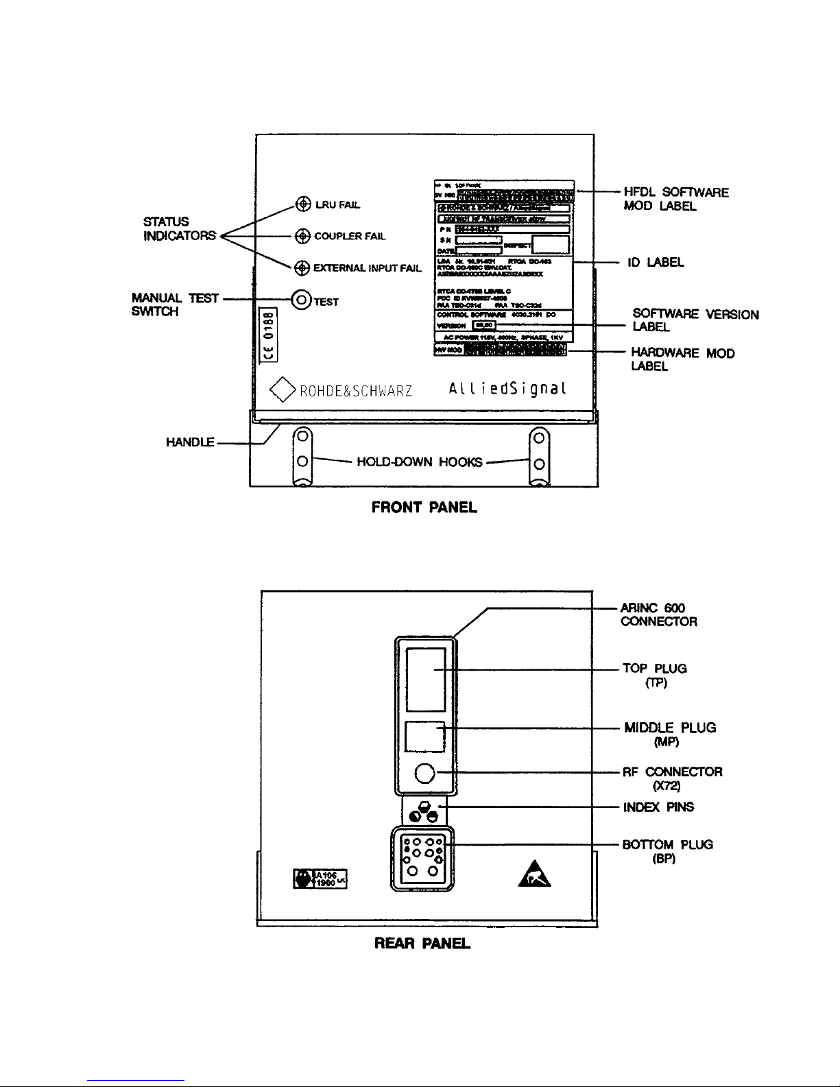
Transceiver Front Panel and Rear Connector
Figure 2
23-12-01
Mar 30/01
Page 23

Honeywell
COMPONENT MAINTENANCE MANUAL
PART NUMBER 964-0452
B. Electrical
The XK516D1 HF Transceiver mode of operation (SSB or AM voice, data, etc.) is controlled
via 2 ARINC 429 serial ports, which are connected on the aircraft to the radio management
panel. The Transceiver is configured for control via ARINC 429 words, both with label 037,
and words with label 205, 206, 207 (installation dependent).
The Transceiver can be connected by means of 2 additional ARINC 429 ports (receive and
transmit) to an on-board central fault display system (CFDS) according to ARINC 604 or to a
central maintenance computer (CMC). There are 3 input discretes (CFDS type programming
pins) that are available in the rear connector to identify the type of aircraft maintenance system. The Transceiver automatically detects which type of aircraft maintenance system (CFDS
or CMC) it is connected to if the CFDS Type input discretes are all open.
Part Number 964-0452-002, 012, and 022 Tranceivers can also be connected to 1 or 2
ACARS Management Units (MU) or Communications Management Units (CMU) by means
of 1 transmit and 2 receive ARINC 429 ports to provide the means to exchange data link
messages with compatible HF Data Link Ground Stations when the Transceiver is operating
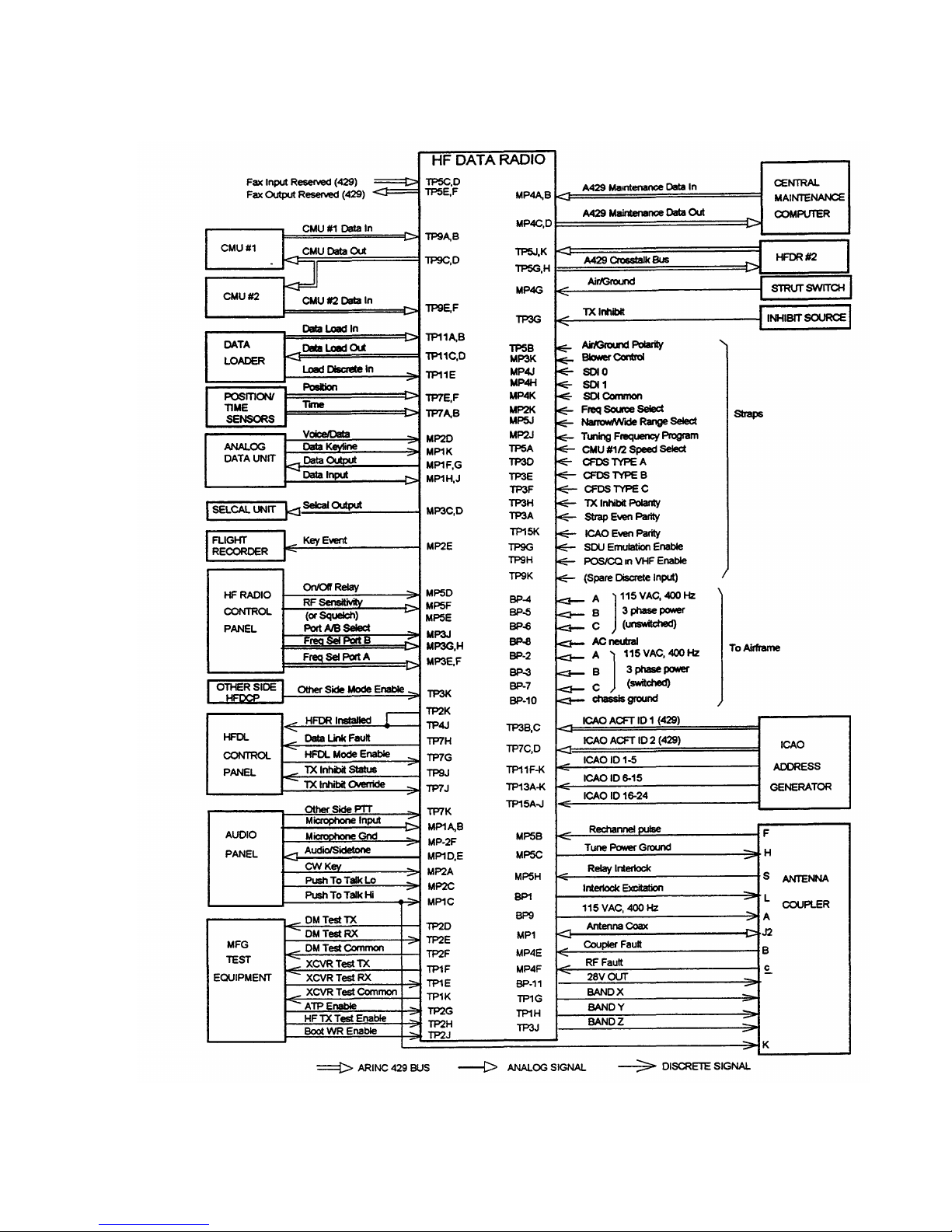
in the internal HFDL Data mode. Refer to Fig. 3 for the HF Voice/Data Radio System Interconnect Diagram, showing all the possible connections to other aircraft systems.
The FK 516 Antenna Coupler (part of XK 516D HF Radio system) is connected to the Transceiver by a coaxial cable and a multiwire control cable. The coaxial cable carries the RF signal and control data for the coupler. The coupler control data consists of serial data messages
sent via the inner conductor of the coaxial cable.The multiwire control cable provides the coupler with 115V/400Hz (single phase) power. The control cable also provides the interlock wiring between couplers in dual HF installations. As an option, for single HF installations, the
multiwire control cable may not be used. In this case, the coaxial cable also carries the Coupler power supply (+28V).
C. Equipment Specifications
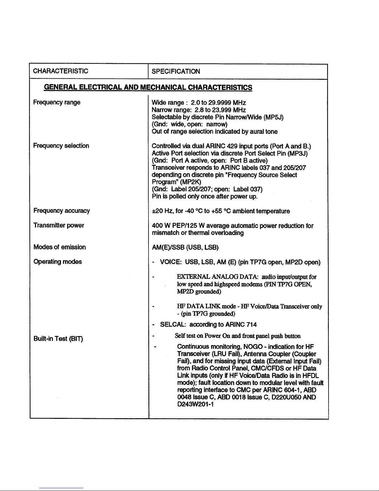
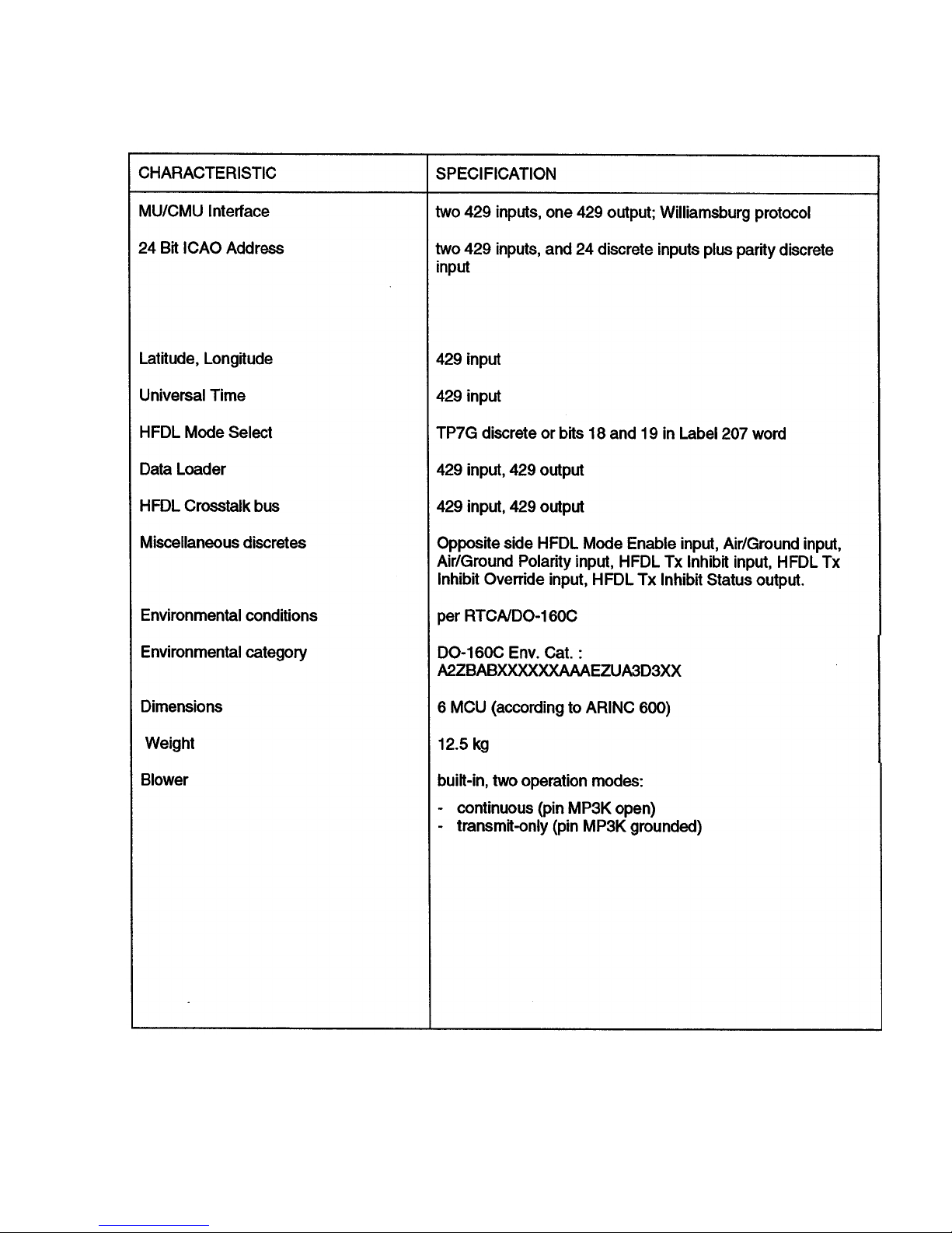
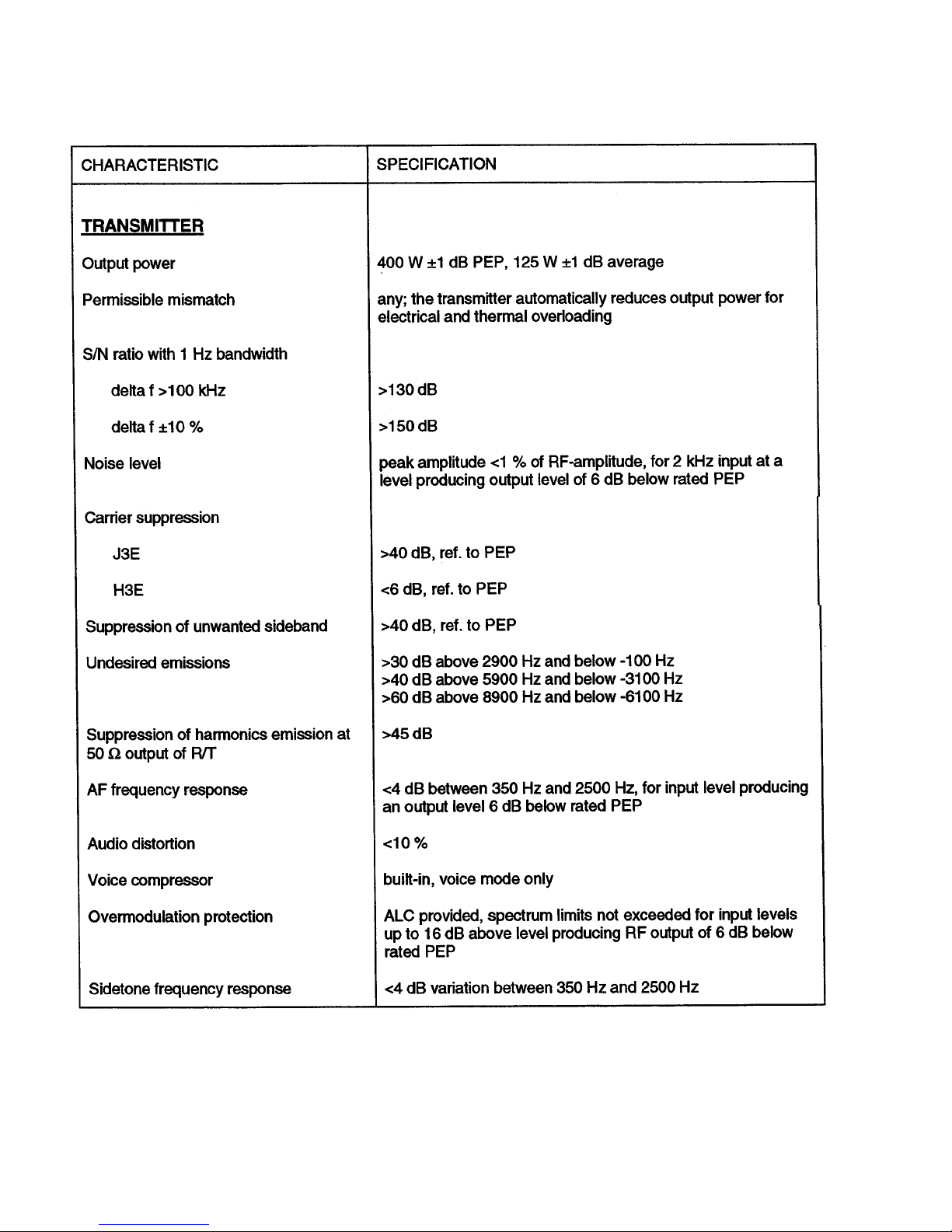
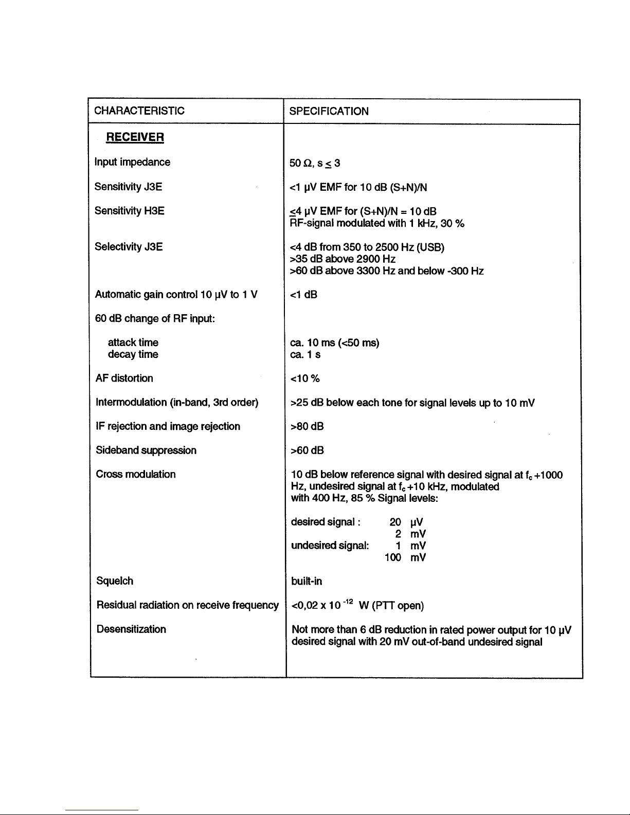
The specifications for the XK516D1 HF Transceiver are listed in Fig. 4.
D. Operation of XK516D1 in Voice Mode
(1) To operate the XK516D1 in Voice Mode, the operator selects either SSB Mode or AM
Mode on the Radio Control Panel and selects the frequency.
(2) The radio tunes to the selected frequency, and the received audio can immediately be
heard on the Audio Management System.
(3) To initiate transmission, the microphone keyline (PTT) must be grounded while speaking
into the microphone.
E. Operation of XK516D1 in HF Data Link Mode
(1) To select HF Data Link Mode, the operator must select DATA mode on the Radio Control
Panel.
(2) When the HFDR is placed in data mode, the HFDR performs an automatic frequency
search from a list of frequencies assigned to HF Data Sync operation. Voice communication through this radio is not possible during this mode of operation.
(3) Based on the aircraft’s position and time of day, the HFDR prioritizes its list of possible
frequencies so that frequencies with the highest probability of propagation are tried first.
1I.B.1516A Page 4
23-12-01
Mar 30/01
Page 24
Honeywell
COMPONENT MAINTENANCE MANUAL
PART NUMBER 964-0452
Interconnect Diagram, HF Voice/Data Radio System
I.B.1516A Page 5
Figure 3
23-12-01
Mar 30/01
Page 25
Honeywell
COMPONENT MAINTENANCE MANUAL
PART NUMBER 964-0452
1I.B.1516A Page 6
Transceiver Specifications
Figure 4 (Sheet 1)
23-12-01
Mar 30/01
Page 26

Honeywell
COMPONENT MAINTENANCE MANUAL
PART NUMBER 964-0452
I.B.1516A Page 7
Transceiver Specifications
Figure 4 (Sheet 2)
23-12-01
Mar 30/01
Page 27
Honeywell
COMPONENT MAINTENANCE MANUAL
PART NUMBER 964-0452
Backup to 516/517 Interface.
Primary mode.
Tune power (MPSC)
1I.B.1516A Page 8
Transceiver Specifications
Figure 4 (Sheet 3)
23-12-01
Mar 30/01
Page 28
Honeywell
COMPONENT MAINTENANCE MANUAL
PART NUMBER 964-0452
I.B.1516A Page 9
Transceiver Specifications
Figure 4 (Sheet 4)
23-12-01
Mar 30/01
Page 29
Honeywell
COMPONENT MAINTENANCE MANUAL
PART NUMBER 964-0452
1I.B.1516A Page 10
Transceiver Specifications
Figure 4 (Sheet 5)
23-12-01
Mar 30/01
Page 30
Honeywell
COMPONENT MAINTENANCE MANUAL
PART NUMBER 964-0452
I.B.1516A Page 11
Transceiver Specifications
Figure 4 (Sheet 6)
23-12-01
Mar 30/01
Page 31

Honeywell
COMPONENT MAINTENANCE MANUAL
PART NUMBER 964-0452
(4) The HFDR then tunes to the first frequency and listens for a periodic uplink (called a
squitter) from the ground station. If no squitter is detected within 32 seconds, the HFDR
tunes to the next frequency on its list.
(5) The HFDR attempts to send a "log-on" downlink when a valid squitter is received. If the
HF Ground Station correctly decodes the downlink, it indicates this in subsequent squitter
uplinks. When this is received by the HFDR, it considers itself logged-on and indicates to
the ACARS MU that data mode is available. The indication on the ACARS display unit
changes from unavailable to available. Transmission of ACARS downlinks and reception
of uplinks is now possible. Note that the HFDR never transmits on an HF frequency
unless the frequency is in its database and a valid squitter is received on that frequency.
(6) If the "log-on" handshake is unsuccessful, the HFDR selects the next frequency from its
list. The HFDR reprioritizes its frequency list when it receives a squitter, since a squitter
contains a list of frequencies that is used by all HF Ground Stations at that moment. The
HFDR indicates that data mode is unavailable after it has exhausted all the frequencies
on its list, but continues to search for a valid connection.
(7) The HFDR begins a search for a new frequency if it fails to detect the periodic squitter or
fails to get a squitter acknowledgement for a downlink.
(8) The existing HF radio system typically shares a common antenna on the aircraft between
the 2 transceivers. If the HFDR detects a Push-To-Talk (PTT) on the other radio operating in voice mode, it delays the transmission of a pending downlink for about 1 minute
(database parameter) to allow the flight crew to complete their voice conversation.
(9) The flight crew may use the HFDR operating in data mode for voice operation at any time
by placing the unit in voice mode via the cockpit control function.
4. Theory of Operation
A. General
The Transceiver performs reception and transmission of voice and data in the frequency
range 2.0MHz to 29.999MHz. The nominal output power of the transmitter is 400W PEP with
a maximum average power of 125W.
A simplified block diagram of the Transceiver is shown in Fig. 5, and a Transceiver interconnect diagram is shown in Fig. 6.
The drive signal for the RF Amplifier, A3, is generated in Receiver/Exciter, A1. The input audio
signal (voice audio from microphone input MP-1A/1B, external audio from AF data input
MP-1H/1J, or internal HFDL data audio from Modem, A10), is digitized in this module and
converted to the necessary modulation signals (SSB or AM(E)) in a signal processor with the
aid of digital signal processing algorithms at a 25kHz IF. This signal undergoes analog conversion again and is up-converted to the final RF level via 2 mixers.
The frequencies of the up-conversion oscillators are generated in a synthesizer according to
the method of digital direct signal synthesis (DDS). This synthesizer also generates the frequencies of the down-conversion oscillators for the receive direction.
1I.B.1516A Page 12
23-12-01
Mar 30/01
Page 32

Honeywell
COMPONENT MAINTENANCE MANUAL
PART NUMBER 964-0452
When receiving, the RF signal is down-converted by means of 2 mixer stages to the second
IF of 25kHz. This IF signal is digitized and undergoes further conditioning in the signal processor. The additional functions, such as filtering, demodulation, and control are achieved by
means of software and appropriate algorithms. The processed signal subsequently undergoes analog conversion again, and is output to the appropriate audio interface (voice audio
output to MP-1D/1E, SELCAL audio output to MP-3C/3D, external data output to MP-1F/1G,
internal HFDL data received audio to Modem, A10).
All external interfaces are passed through EMC Filter, A7, to suppress spurious signals.
The internal BITE system of the Transceiver detects a defective LRU by means of continuous
monitoring, and localizes the fault down to functional units on modules (SRUs). In addition,
I.B.1516A
Block Diagram (Simplified), Transceiver
Figure 5
23-12-01
Page 13
Mar 30/01
Page 33

Honeywell
COMPONENT MAINTENANCE MANUAL
PART NUMBER 964-0452
built-in tests can be initiated, manually via a front panel test button, or from the aircraft maintenance system, via an ARINC 429 interface.
The results of the continuous monitoring are permanently supplied to the CFDS/CMC in the
normal mode, according to ARINC 604. In the interactive mode, the faults of previous flight
legs, test initiation, and more detailed fault information (troubleshooting data) are displayed.
The BITE system, and modes of operation, are controlled by the Controller Module, A8.
The Transceiver is configured for connection to a 115V, 400Hz, 3-phase, approximately
1000W supply. The internal voltages are generated in the Power Supply, A4.
B. Simplified Theory of Operation
The primary functions of the individual modules in the Transceiver are described here:
(1) Receiver/Exciter, A1
(a) General
The key signal processing functions for transmitting and receiving are executed in
Receiver/Exciter, A1. The signal progression for receive and transmit operation is
outlined in functional diagram of Fig. 7 .
In the transmit mode, these functions are involved:
• Modulation (AM(E)), SSB)
• Automatic level control
• Voice compressor
• Signal synthesis for conversion oscillators
• Conversion of modulated signal to 2nd IF (25kHz), 1st IF (40.025MHz),
and RF frequency.
In the receive mode, these functions are involved:
• Demodulation (SSB, AM(E))
• Automatic gain control
• IF filteringSignal synthesis for conversion oscillators
• Conversion of RF signal to 1st IF (40.025MHz) and 2nd IF (25kHz)
All the signal processing functions performed on the 25kHz frequency are executed
in a signal processor as described here:
The 2nd IF signal (25kHz) is digitized by an A/D converter (100kHz sampling rate)
and further conditioned in the signal processor. After processing, the signal again
undergoes conversion in the D/A converter (12.5kHz sampling rate), and is supplied
to the audio outputs (audio, SELCAL, data) as an audio signal.
In transmission mode, a signal (audio, data) present at the audio inputs is digitized
by means of an A/D converter (100kHz sampling rate), and converted to the 25kHz
2nd IF signal in the signal processor.
The RF signal is supplied to the 1st mixer via a 30MHz, low-pass filter, and convert-
ed to the 1st IF at 40.025MHz with the aid of the conversion oscillator (42.025MHz)
to 7 0.02499MHz). The conversion oscillator is derived from voltage-controlled oscillator (VCO3). VCO3 forms part of a phase-locked loop (PLL), whose reference
frequency is derived from a signal generated by direct digital synthesis (DSS).
I.B.1516A
23-12-01
Page 14
Mar 30/01
Page 34

Honeywell
COMPONENT MAINTENANCE MANUAL
PART NUMBER 964-0452
I.B.1516A Page 15/16
Mar 30/01
23-12-01
Interconnect Diagram, Transceiver
Figure 6
KEY INTERLOCK
EMC
FILTER
A7
TP-7B
HFDR #2 IN HI
HFDR #2 IN LO
HFDR #2 OUT HI
HFDR #2 OUT LO
TP-5J
TP-5K
TP-5G
TP-5H
CMU #1 DATA IN HI
TP-9A
TP-9B
CMU #1 DATA IN LO
CMU #2 DATA IN HI
CMU #2 DATA IN LO
TP-9F
TP-9E
CMU DATA OUT HI
TP-9C
CMU DATA OUT LO
TP-9D
TP-5A
CMU BUS SPEED
TP-7A
GMT IN HI
GMT IN LO
TP-7E
TP-7F
POSITION IN HI
POSITION IN LO
ICAO ID#1 IN HI
ICAO ID#1 IN LO
ICAO ID#2 IN HI
ICAO ID#2 IN LO
TP-3B
TP-3C
TP-7C
TP-7D
TP-11A
TP-11B
TP-11C
TP-11D
TP-11E
DATA LOADER IN HI
DATA LOADER IN LO
DATA LOADER OUT HI
DATA LOADER OUT LO
DATA LOAD DISCRETE
TP-5C
TP-5D
TP-5E
TP-5F
FAX REC HI
FAX REC LO
FAX TRANS HI
FAX TRANS LO
TP-9J
TP-7K
TP-3G
TP-3H
TP-7J
TP-15K
*
TP-4J
TP-2K
(24) ICAO DISCRETES
TX INHIBIT STATUS
OTHER SIDE PTT
TX INHIBIT
TX INHIBIT POLARITY
TX INHIBIT OVERRIDE
ICAO EVEN PARITY
HFDR INSTALLED
INTERFACE
A9
AIRBORNE
DATALINK
PROCESSOR
A2
HF
MODEM
A10
CONTROLLER
A8
OTHER SIDE
MODE EN
HFDL MODE ENABLE
FREQ PORT A HI
FREQ PORT A LO
FREQ PORT B HI
FREQ PORT B LO
CFDS TYPE A
CFDS TYPE B
CFDS TYPE C
BITE IN HI
BITE IN LO
BITE OUT HI
BITE OUT LO
PTT HI
PTT OUT
KEY EVENT
VOICE DATA
DATA KEY
PORT SELECT
GROUND/AIR
GROUND/AIR POLARITY
WIDE RANGE SELECT
FREQ SOURCE SELECT
SQUELCH
SENSITIVITY
DATA LINK FAULT
SDI O
SDI 1
STRAP EVEN PARITY
BAND Z
BAND Y
BAND X
KEY INTERLOCK
TUNE POWER
RECHANNEL PULSE
CW KEY
(24) ICAO DISCRETES
HDFR INSTALLED
BITE IN HI
BITE IN LO
BITE OUT HI
BITE OUT LO
ACTIVE FREQ PORT HI
ACTIVE FREQ PORT LO
ADP PRESENT
ADP COMM HI
ADP COMM LO
INT HFDR FAULT
INT SDI0
INT SDI1
TUNE FAIL
TUNE IN PROGRESS
FREQ SRC SEL
GND/AIR
INTFC SPARE 1
INTFC SPARE 2
ICAO EVEN PARITY
TX INHIBIT OVERRIDE
TX INHIBIT POLARITY
TX INHIBIT
OTHER SIDE PTT
HFDR#2 IN HI
HFDR#2 IN LO
HFDR#2 OUT HI
HFDR#2 OUT LO
CMU#1 DATA IN HI
CMU#1 DATA IN LO
CMU#2 DATA IN HI
CMU#2 DATA IN LO
CMU DATA OUT HI
CMU DATA OUT LO
CMU BUS SPEED
GMT IN HI
GMT IN LO
POSITION IN HI
POSITION IN LO
ICAO ID#1 IN HI
ICAO ID#1 IN LO
ICAO ID#2 IN HI
ICAO ID#2 IN LO
DATA LOADER IN HI
DATA LOADER IN LO
DATA LOADER OUT HI
DATA LOADER OUT LO
DATA LOAD DISCRETE
FAX REC HI
FAX REC LO
FAX TRANS LO
FAX TRANS HI
TX INHIBIT STATUS
+15V
-15V
+5V
GND
HFM RESET
HFM PRESENT
HFM FAULT
HFM RX ACTIVE
HFM TX ACTIVE
ADP SPARE 1
ADP SPARE 2
OTHER SIDE MODE EN
DM TEST
DATA ENABLE
PROCESSOR BUS
RECPLS
STRUT
DATA KEY MON
RESET OUT
INT DATA KEY
POWER
SUPPLY
A4
EMC
FILTER
A7
RECEIVER/
EXCITER
A1
POWER
AMPLIFIER
A3
SPARE DISCRETE INPUT 1
SPARE DISCRETE INPUT 2
SPARE DISCRETE INPUT 3
DM TEST TX
RF IN/OUT
AC FAIL
RESET
DM TEST RX
ATP ENABLE
HF TX TEST ENABLE
BOOT WR ENABLE
POS/CQ IN VHF ENABLE
INT DATA KEY
BLOWER
BLOWER
DATA (AF) IN
DATA (AF) IN HI
STRAP EVEN PARITY
BAND Z
BAND Y
BAND X
TUNE POWER
RECHANNEL PULSE
CW KEY
SDI/ICAO COMMON
SDI 1
SDI 0
DATA LINK FAULT
+15v
-15v
+5v
GND
+15v
-15v
+5v
GND
MFG RESERVED CONNECTIONS
RF IN/OUT
+28v
+50v
+5v
GND
+15v
-15v
BP-3
BP-4
BP-5
BP-6
BP-8
BP-9
BP-10
BP-2
BP-7
115V UNSWITCHED A
115V SWITCHED A
115V SWITCHED B
115V SWITCHED C
CHASSIS GND
115V OUT
AC COLD
115V UNSWITCHED B
115V UNSWITCHED C
+15v
-15v
+5v
GND
+15v
-15v
+5v
GND
TX TIM
RTS
TX DATA
CTS
RX DATA
DATA (AF) OUT
TX DATA AF
RX DATA AF
DATA (AF) IN LO
DATA (AF) OUT HI
DATA (AF) OUT LO
MIKE IN LO
MIKE IN HI
MIKE GND
SENSITIVITY
SQUELCH
FREQ SOURCE SELECT
WIDE RANGE SELECT
GROUND/AIR POLARITY
GROUND/AIR
PORT SELECT
DATA KEY
VOICE DATA
KEY EVENT
PTT LO
PTT HI
BITE OUT LO
BITE OUT HI
BITE IN LO
BITE IN HI
CFDS TYPE C
CFDS TYPE B
CFDS TYPE A
FREQ PORT B LO
FREQ PORT B HI
FREQ PORT A LO
FREQ PORT A HI
HFDL MODE ENABLE
OTHER SIDE MODE EN
AUDIO OUT HI
AUDIO OUT LO
SELCAL HI
SELCAL LO
ON/OFF RELAY
COUPLER FAULT
RF FAULT
28V OUT
INTL EXCIT
(7) TEST ID
SPARE DISCRETE INPUT
SDU EMULATION ENABLE
BOOT WR ENABLE
HF TX TEST ENABLE
ATP ENABLE
DM TEST COM
DM TEST RX
DM TEST TX
TP-2D
TP-2E
TP-2F
TP-2G
TP-2H
TP-2J
TP-9G
TP-9H
TP-9K
TP-1F
TP-1E
TP-1K
TEST COM
TEST TX
TEST RX
TEST TX
TEST RX
+28v
+50v
+5v
GND
+15v
-15v
+28v
+5v
GND
+15v
-15v
MIKE IN HI
MIKE IN LO
AUDIO OUT
SELCAL
MP-4D
MP-1C
MP-2C
MP-2E
MP-2D
MP-1K
MP-3J
MP-4G
TP-5B
MP-2K
MP-5J
MP-5E
MP-5F
TP-7H
MP-4H
MP-4J
MP-4K
MP-2A
MP-5B
MP-5C
MP-5H
* *
TP-1G
TP-1H
TP-3K
TP-7G
MP-3E
MP-3F
MP-3G
MP-3H
TP-3D
TP-3E
TP-3F
MP-4A
MP-4B
MP-4C
TP-3J
TP-3A
MP-3K
MP-1H
MP-1J
MP-1F
MP-1G
MP-1A
MP-1B
MP-2F
MP-1D
MP-1E
MP-3C
MP-3D
MP-5D
MP-4E
MP-4F
BP-11
BP-1
ICAO ID 6
ICAO ID 7
ICAO ID 8
ICAO ID 9
ICAO ID 10
TP-13A
TP-13B
TP-13C
TP-13D
TP-13E
ICAO ID 11
ICAO ID 12
ICAO ID 13
ICAO ID 14
ICAO ID 15
TP-13F
TP-13G
TP-13H
TP-13J
TP-13K
ICAO ID 16
ICAO ID 17
ICAO ID 18
ICAO ID 19
ICAO ID 20
TP-15A
TP-15B
TP-15C
TP-15D
TP-15E
ICAO ID 21
ICAO ID 22
ICAO ID 23
ICAO ID 24
TP-15F
TP-15G
TP-15H
TP-15J
**
UNTID0
UNTID1
UNTID2
UNTID3
UNTID4
UNTID5
UNTID6
TP-2C
TP-1A
TP-1B
TP-1C
TP-1D
TP-2A
TP-2B
*
ICAO ID 1
ICAO ID 2
ICAO ID 3
ICAO ID 4
ICAO ID 5
TP-11F
TP-11G
TP-11H
TP-11J
TP-11K
Page 35

Honeywell
COMPONENT MAINTENANCE MANUAL
PART NUMBER 964-0452
I.B.1516A Page 17/18
Mar 30/01
23-12-01
Functional Diagram, Receiver/Transmitter, A1
Figure 7
Page 36

Honeywell
COMPONENT MAINTENANCE MANUAL
PART NUMBER 964-0452
I.B.1516A Page 19/20
Mar 30/01
23-12-01
Block Diagram, Power Amplifier Board, A3
Figure 8
Page 37

Honeywell
COMPONENT MAINTENANCE MANUAL
PART NUMBER 964-0452
Along with the reference signal, the phase comparator of the PLL is also supplied
with the down-converted frequency of VCO3. The mixing frequency for this down
conversion is obtained from a second PLL. The reference frequency of the 2nd PLL
is derived from a crystal oscillator (10Mhz), which is scaled down by a factor of 100.
The 1st IF of 40.025MHz is supplied to the 2nd mixer via a variable amplifier and
converted to the 2nd IF of 25kHz. The mixing frequency for this mixer (40MHz) is
also generated with the aid of a PLL, whose reference frequency (1MHz) is derived
from a crystal oscillator.
The 2nd IF signal (25kHz) is digitized by a 16-bit A/D converter and supplied to the
signal processor. The demodulation and conversion of the signal to an audio frequency (AF) signal is executed in the signal processor.
The principal functions performed in the signal processor are:
• Demodulation (SSB, AM)
• IF filtering for audio, SELCAL, and AM
• Automatic gain control (90dB dynamic range)
• Squelch
• The audio signal is applied via D/A converter (sampling rate 12.5kHz)
to the audio, SELCAL, and data outputs
(b) Transmit Mode
The audio signal (voice or data) is digitized by the 16-bit A/D converter (100kHz
sampling rate) and read into the signal processor.
The functions that are performed in the signal processor by means of software are:
• Filtering of the audio signal
• Voice compression
• Automatic level control
• Conversion to 25kHz IF frequency
• Conversion of SSB or AM(E) signal
• Mixing to 25kHz
The 25kHz IF signal thus created undergoes analog conversion in a D/A converter
(sampling rate 100kHz). The signal is finally converted to the frequency in the 2.0
to 29.9999MHz range.
The conversion oscillators are generated in the same way as for receive operation.
The output signal of Receiver/Exciter, A1, is a –7dBm (nominal) signal, which is
supplied to the Power Amplifier, A3.
The Receiver/Exciter module is connected to the Controller module, A8, via the
module bus, where all settings are made; e.g., frequency, operating mode, transmission mode, BIT functions.
BIT results and the signal level can be determined via the module bus.
(2) Power Amplifier, A3
Power Amplifier, A3, is composed of Amplifier Board, A31, Harmonic Filter, A32, and Amplifier Control, A33. Refer to Fig. 8 for block diagram.
I.B.1516A
23-12-01
Page 21
Mar 30/01
Page 38

Honeywell
COMPONENT MAINTENANCE MANUAL
PART NUMBER 964-0452
(a) Amplifier Board, A31
The Amplifier Board amplifies the RF input from Receiver/Exciter, A1, with a level
of –7dBm ± 3dB Peak Envelope Power (PEP) or Continuous Wave (CW) to a maximum output power of 125W continuous wave (+51dBm) or 400W +0.5dB PEP
(56dBm +0.5dB). It is composed of 4 amplifier stages, the final stage operates in
push-pull mode. A voltage-controlled attenuator is inserted between the 1st amplifier stage and the 2nd amplifier stage with the function of regulating the output power of Amplifier Board, A31, at a constant level, depending upon the ALC voltage
generated by Amplifier Control, A33.
Amplifier board, A31, also contains a number of monitoring and measuring circuits.
(b) Cooling
The preamplifier and final stage transistors are cooled by a heat sink. An internal
blower ensures the airflow through the Transceiver, and maintains proper cooling
of Power Amplifier, A3, during transmit operations.
(c) Harmonic Filter, A32
Harmonic Filter, A32, contains 1 transmit/receive relay, 7 low-pass filters, 1 or 2 of
which are switched on in order to suppress the harmonics in the RF signal path, depending upon the transmission frequency, as well as a directional coupler for measuring the forward and reflected power.
(d) Modem
The Harmonic Filter, A32, also contains a modem with frequency-division multiplex-
ing, permitting simultaneous bidirectional data transfer between transceiver and antenna coupler vial the coaxial line.
(e) Amplifier Control, A33
Amplifier Control, A33, provides the interface between Controller, A8, and Amplifier
Board, A31, and Harmonic Filter, A32. This connection links the information coming
via the module data bus with internal module signals to obtain control signals for the
Amplifier Board and Harmonic Filter. In addition, the ALC control voltage for regulating the transceiver output power is generated here from various analog measured signals from Amplifier board, A31, and Harmonic Filter, A32.
(3) Power Supply, A4
The Power Supply, A4, is composed of a 3-phase transformer, Regulator Board, A41,
and Mains Filter, A42. The transformer is delta-connected at the input end and the 5 secondary windings are all star-connected. The star point for secondary winding 5 is directly
configured on the transformer; the star points of the other 4 secondary windings are located on the Regulator Board, A41.
The outputs of secondary windings 1 through 4 are connected to the Regulator Board,
A41, where the various supply voltages are generated by means of rectifiers and series
regulators. Secondary winding 5 of the transformer is configured as a 3-phase power output in order to supply the RF power transistors in Power Amplifier, A3. The rectifiers and
filters are also located on Power Amplifier, A3.
I.B.1516A
23-12-01
Page 22
Mar 30/01
Page 39

Honeywell
COMPONENT MAINTENANCE MANUAL
PART NUMBER 964-0452
(4) LED Board, A5
The LED Board, A5, contains the 3 LED indicators, which indicate:
• LRU Fail
• Coupler Fail
• Control Fail
The LED Board is connected to the Motherboard via a ribbon cable and connector, and
also contains the switch for manual test initiation (X14).
(5) Motherboard, A6
Motherboard, A6, consists of an 8-layer board, containing all signal links and power supply lines to the individual modules. The modules are contacted via indirect plug-in connections. A coaxial cable provides the RF link between the Receiver/Exciter, A1, and the
Power Amplifier, A3. All signals present at the ARINC 600 rear connector are supplied to
the EMC Filter, A7, via 2 ribbon cables (plug-in connection W74, W76).
(6) EMC Filter, A7
The EMC Filter consists of a rear panel and the Filter board, which connects the external
cabling with the basic modules of the Transceiver.
The Filter board prevents the transmission of spurious signals in both directions by
means of RCR and LCR low pass filters. All lines to the ARINC 600 rear connector are
provided with overvoltage limitation. Lines that do not require filtering are decoupled with
resistors to prevent operational disturbances.
In addition, the Filter board contains an LF board as a subassembly for matching adjustable symmetrical LF inputs and outputs to the 0dBm interface of the Transceiver.
(7) Controller D, A8, and Interface D, A9
The control functions of the Transceiver are performed by the Controller D and Interface
D modules. The 2 modules are interconnected by means of the Motherboard, A6.
(a) Controller D, A8
Controller D, A8, accommodates the processor, the memories, the module bus for
driving the RF assemblies, as well as the serial interfaces for communication with
the FK 516 Antenna Coupler and test interface.
(b) Controller D, A8, Performance Characteristics
• Processor 80C186 with 16MHz clock frequency
• 64 kByte RAM
• 128 kByte EPROM
• 8 kByte EEPROM
• Serial interface to antenna coupler
• Serial test interface
• A/D converter for squelch and sense
• 16 bit module bus for controlling the RF assemblies
• x2 ARINC 429 inputs, 1 ARINC 429 output, with transfer rate of 12.5kBps
• Discrete inputs/outputs
I.B.1516A
23-12-01
Page 23
Mar 30/01
Page 40

Honeywell
COMPONENT MAINTENANCE MANUAL
PART NUMBER 964-0452
(c) Interface D, A9
Interface, A9, houses the serial ARINC inputs and outputs, as well as a number of
discrete input and output lines.
(8) ON/OFF Module, A15
The purpose of the ON/OFF Module, A15, is to provide an optional On-Off switching function to the Transceiver via discrete input MP-5D. It also provides the supply voltage for
the internal blower.
(9) Data Module (PN 964-0452-002, 012, and 022)
The Data Module consists of the Airborne Datalink Processor (ADP) Circuit Card Assembly (CCA), A2, and the HF Modem CCA, A10. When the Data Module components are
installed into an XK516D1 HF Transceiver, they allow the radio to maintain all the functions of the Voice version Transceiver, but in addition, allows the Transceiver to operate
in HF Data Link (HFDL) mode as specified by ARINC 753 and ARINC 635.
The Data Module implements the airborne side of the HF air/ground protocol including
the automatic frequency selection and data link establishment.
C. Detailed Theory of Operation
(1) Receiver/Exciter, A1
The Receiver/Exciter, A1, contains the entire signal path in the recieve direction, the
small-signal path in the transmit direction, and the synthesizer.
(a) Synthesizer
The frequencies required for conversion in the receive and transmit paths are pro-
cessed in the synthesizer. These are the "1. osc.", a frequency that can be modified
in 100Hz increments from 42025 to 70024.9kHz for the first mixer, a fixed frequency
of 40MHz for the 2nd mixer, and a fixed frequency of 8MHz as the clock frequency
for the signal processor. In addition a 2MHz signal is generated for the assembly
self-test (BIT). All these frequencies are derived from a 10MHz crystal oscillator.
The data required to set the "1. osc." are input with active moduLe select 1 (MS1 =
LOW) via the bidirectional data bus (16 bit, 3 addresses).
1 Crystal oscillator
The crystal oscillator is a D-TCXO (digital temperature-compensated crystal oscillator) with a frequency of 10MHz. The frequency deviation is less than 0.5ppm
in the temperature range from –40°C to +85°C. The crystal oscillator is supplied
with a voltage of +12V by fixed voltage regulator, N11. Frequency adjustment is
effected by potentiometer, R239. The output frequency (5V CMOS level) is divided by 5 and then by 2 in divider, D5-B. The 2MHz signal is required for the
self-test; the 1MHz signal to process the frequencies.
2 Loop 1
The fixed frequencies of 40MHz and 8MHz are produced in this Phase-Locked
Loop (PLL ). Ref. Fig. 9 for block diagram.
The Voltage-Controlled Oscillator (VCO) is essentially composed of transistor,
V64, and the oscilLator circuit, which can be retuned with tuning diode, V61. The
I.B.1516A
23-12-01
Page 24
Mar 30/01
Page 41

Honeywell
COMPONENT MAINTENANCE MANUAL
PART NUMBER 964-0452
I.B.1516A Page 25/26
Mar 30/01
23-12-01
Block Diagram, Synthesizer Loop 1
Figure 9
Page 42

Honeywell
COMPONENT MAINTENANCE MANUAL
PART NUMBER 964-0452
I.B.1516A Page 27/28
Mar 30/01
23-12-01
Block Diagram, Synthesizer Loop 2 and 3
Figure 10
Page 43

Honeywell
COMPONENT MAINTENANCE MANUAL
PART NUMBER 964-0452
output signal of 40MHz is brought to TTL level by transistors, V62 and V63, respectively, and supplied to 4:1 divider, D16, or 5:1 divider, D17. The 10MHz output frequency of the 4:1 divider is divided by 2 in D5-A, and then by 5. The 5MHz
signat is required as a clock pulse for digital direct synthesis (DDS) in loop 3.
The 1MHz output frequency from D5-A is supplied with the 1MHz signal from
the crystal oscillator to phase comparator, D15. If the frequency and phase of
the 2 input signals are the same, the output of the phase comparator is in the
tristate condition (high impedance).
If the signal produced by the VCO is advanced in phase; i.e, the VCO frequency
is too high, the output of the phase comparator assumes a LOW level for the
duration of the phase difference, and then returns to the tristate condition.
This brief LOW impulse results in a slight increase in output voltage at the output
of inverted integrator, N15-A. Consequently, the U-LOOP1 voltage, which is
supplied to tuning diode, V61, is reduced at the output of inverted amplifier,
N15-B, thus causing the frequency of the VCO to be decreased again. In this
way, the frequency of the VCO is synchronized with the accuracy of the crystaL
oscilLator at 40MHz.
The 40MHz signal, coupled out of the capacitive divider of the oscillator circuit,
is amplified in cascade amplifiers, V69, V70, V65, and drives the 2nd mixer. V60
is connected as an inverter and is used to reset the divider.
3 Loop 2
This loop generates an auxiliary frequency, which is a multiple of 100kHz between 41.8MHz and 69.8MHz. Ref. Fig. 10 for block diagram.
The VCO, with transistor, V20, is roughly preset and synchronized at the exact
frequency with tuning diode, V22. A data word is stored in Latch, D25, for the
presetting, depending upon the frequency set at the CDU according to Fig. 11.
The latch outputs assigned to data D9 to D12 connect to ground the 4 binary
scaled resistors, A13R11, A13R63, A13R57, and A13R23, via transistors,
A13V3, A13V1, A13V16, and A13V17.
Voltage, UST2, can therefore have 16 values, the lowest, about +6V, when all 4
data are high, and the highest, +12V, when all 4 data are LOW. It is present via
R78 at tuning diodes V17 and V18.
If a LOW is stored for data, D13, transistor, A13V18, is through-connected, and
a current of +5V flows on wire, VCO5, via R93 through switching diode, V14,
and coil, L3 to ground. As a result, C80 and trimmer, C81, are connected to the
oscillator circuit. If a HIGH was stored for data, D13, switching diode, V14, is disabled via A13R28 with –9.1V. Similarly, a LOW for data, D14, results in capacitor
C95 and trimmer, C76, being connected to the oscillator circuit.
If a LOW is stored for data, D15, coil, L2, is connected parallel to coil, L3. To
prevent the amplitude of oscillations from falling as a result of this reduction in
the L/C ratio, resistor, A13Rl3, is by-passed with A13V6, and consequently, the
direct current in transistor, V20, is increased.
I.B.1516A
23-12-01
Page 29
Mar 30/01
Page 44

Honeywell
COMPONENT MAINTENANCE MANUAL
PART NUMBER 964-0452
FREQUENCY (MHZ) DATA WORD
FROM TO D15 D14 D13 D12 D11 D10 D9 D8
2000 2049.9 1 0 0 0 0 0 1 1
2050 2299.9 1 0 0 0 0 0 0 1
2300 2499.9 1 0 1 1 1 1 0 1
2500 2649.9 1 0 1 1 1 0 0 1
2650 2799.9 1 0 1 0 1 1 1 1
2800 2949.9 1 0 1 0 1 1 0 1
2950 3099.9 1 0 1 0 1 0 1 1
3100 3299.9 1 0 1 0 1 0 0 1
3300 3449.9 1 0 1 1 0 1 1 1
3500 3649.9 1 0 1 1 0 1 0 1
3650 3849.9 1 0 1 1 0 0 1 1
3850 4049.9 1 0 1 1 0 0 0 1
4050 4299.9 1 0 1 0 0 1 1 1
4300 4549.9 1 0 1 0 0 1 0 1
4550 4849.9 1 0 1 0 0 0 1 1
4850 5149.9 1 0 1 0 0 0 0 1
5150 5439.9 1 1 0 1 1 0 1 0
5440 5649.9 1 1 0 0 1 1 1 0
5650 5849.9 1 1 0 0 1 1 0 0
5850 6049.9 1 1 0 0 1 0 1 0
6050 6249.9 1 1 0 0 1 0 0 0
6250 6449.9 1 1 0 1 0 1 1 0
6450 6649.9 1 1 0 1 0 1 0 0
6650 6949.9 1 1 0 1 0 0 1 0
6950 7199.9 1 1 0 1 0 0 0 0
7200 7499.9 1 1 0 0 0 1 1 0
7500 7819.9 1 1 0 0 0 1 0 0
7820 8199.9 1 1 0 0 0 0 1 0
8200 8499.9 1 1 0 0 0 0 0 0
8500 8699.9 1 1 1 1 1 1 1 0
8700 8849.9 1 1 1 1 1 0 0
8850 9099.9 1 1 1 1 1 0 1 0
9100 9299.9 1 1 1 1 1 0 0 0
9300 9499.9 1 1 1 0 1 1 1 0
9500 9719.9 1 1 1 0 1 1 0 0
I.B.1516A
Frequency Range Corresponding Data Word
Figure 11 (Sheet 1)
23-12-01
Page 30
Mar 30/01
Page 45

Honeywell
COMPONENT MAINTENANCE MANUAL
PART NUMBER 964-0452
FREQUENCY (MHZ) DATA WORD
FROM TO D15 D14 D13 D12 D11 D10 D9 D8
9720 9949.9 1 1 1 0 1 0 1 0
9950 10199.9 1 1 1 0 1 0 0 0
10200 10449.9 1 1 1 1 0 1 1 0
10450 10749.9 1 1 1 1 0 1 0 0
10750 11099.9 1 1 1 1 0 0 1 0
11100 11449.9 1 1 1 1 0 0 0 0
11450 11849.9 1 1 1 0 0 1 1 0
11850 12299.9 1 1 1 0 0 1 0 0
12300 12799.9 1 1 1 0 0 0 1 0
12800 13249.9 1 1 1 0 0 0 0 0
13250 13469.9 0 0 0 1 1 1 1 1
13470 13729.9 0 0 0 1 1 0 1 1
13730 13999.9 0 0 0 0 1 1 1 1
14000 14299.9 0 0 0 0 1 0 1 1
14300 14599.9 0 0 0 1 0 1 1 1
14600 14799.9 0 0 0 1 0 1 0 1
14800 15019.9 0 0 0 1 0 0 1 1
15020 15299.9 0 0 0 1 0 0 0 1
15300 15549.9 0 0 0 0 0 1 1 1
15550 15859.9 0 0 0 0 0 1 0 1
15860 16119.9 0 0 0 0 0 0 1 1
16120 16349.9 0 0 0 0 0 0 0 1
16350 16599.9 0 0 1 1 1 1 1 1
16600 16879.9 0 0 1 1 1 0 1 1
16880 17249.9 0 0 1 0 1 1 1 1
17250 17599.9 0 0 1 0 1 0 1 1
17600 17999.9 0 0 1 1 0 1 1 1
18000 18249.9 0 0 1 1 0 1 0 1
18250 18499.9 0 0 1 1 0 0 1 1
18500 18799.9 0 0 1 1 0 0 0 1
18800 19149.9 0 0 1 0 0 1 1 1
19150 19499.9 0 0 1 0 0 1 0 1
19500 19899.9 0 0 1 0 0 0 1 1
19900
20199.9
20200 20399.9
0 1 0 1 1 0 1 0
0 1 0 1 1 0 0 0
I.B.1516A
Frequency Range Corresponding Data Word
Figure 11 (Sheet 2)
23-12-01
Page 31
Mar 30/01
Page 46

Honeywell
COMPONENT MAINTENANCE MANUAL
PART NUMBER 964-0452
FREQUENCY (MHZ) DATA WORD
FROM TO D15 D14 D13 D12 D11 D10 D9 D8
20400 20599.9
20600 20849.9
20850 21099.9
21100 21349.9
21350 21599.9
21600 21899.9
21900 22199.9
22200 22599.9
22600 22999.9
23000 23449.9
23450 23999.9
24000 24339.9
24340 24699.9
24700 24999.9
25000 25199.9
25200 25499.9
25500 25749.9
25750 26039.9
26040 26399.9
26400 26699.9
26700 27099.9
27100 27499.9
27500 27999.9
28000 28499.9
28500 29099.9
29100 29699.9
29700 29999.9
0 1 0 0 1 1 1 0
0 1 0 0 1 1 0 0
0 1 0 0 1 0 1 0
0 1 0 0 1 0 0 0
0 1 0 1 0 1 1 0
0 1 0 1 0 1 0 0
0 1 0 1 0 0 1 0
0 1 0 1 0 0 0 0
0 1 0 0 0 1 1 0
0 1 0 0 0 1 0 0
0 1 0 0 0 0 1 0
0 1 0 0 0 0 0 0
0 1 1 1 1 1 0 0
0 1 1 1 1 0 1 0
0 1 1 1 1 0 0 0
0 1 1 0 1 1 1 0
0 1 1 0 1 1 0 0
0 1 1 0 1 0 1 0
0 1 1 0 1 0 0 0
0 1 1 1 0 1 1 0
0 1 1 1 0 1 0 0
0 1 1 1 0 0 1 0
0 1 1 1 0 0 0 0
0 1 1 0 0 1 1 0
0 1 1 0 0 1 0 0
0 1 1 0 0 0 1 0
0 1 1 0 0 0 0 0
To counteract an excessive decline in the tuning transconductance in the event
of the oscillator circuit capacity being enlarged, tuning diode, V23, is connected
to tuning diode, V22, by connecting C95 and C76. This is effected with data, D8,
on HIGH via level shifter, A13N2-A, and FET switch, V21.
The VCO drives 2 base stages. The signal is supplied to loop 3 via V26, and an
ECL level is generated in V34, which drives the loop divider.
I.B.1516A
Frequency Range Corresponding Data Word
Figure 11 (Sheet 3)
23-12-01
Page 32
Mar 30/01
Page 47

Honeywell
COMPONENT MAINTENANCE MANUAL
PART NUMBER 964-0452
The Loop divider consists of D19, a predivider, whose division ratio can be varied between 11:1 and 10:1, and D6, a synthesizer module, containing an A divider, an N divider, a phase comparator, and an R divider.
The division ratios of D6 are set serially with 8 addressed 4-bit words, which are
processed in gate array, D99.
The predivider is switched from the A divider of the synthesizer module. The signal from predivider, D19, drives the A and N dividers. The frequency of the VCO
is divided by 11 A times and divided by 10 N-A times.
The entire division ratio M, therefore, is: 11 x A + 10 x (N–A) = 10 x N + A
The 1MHz reference frequency for loop 2 is supplied to the synthesizer module
via oscillator circuit L31/C89, and divided by 10 to obtain 100kHz in the R divider
of the synthesizer module.
The phase comparator, with subsequent integrator and amplifier, functions in
the same way as described for loop 1. The VCO is synchronized to M x 100kHz
with control voltage U-LOOP2.
4 DDS (digital direct synthesis)
A variable frequency is generated between 220kHz and 319.9kHz in 100Hz increments with the 5MHz clock pulse in ICs, D99, D26, D24, and D23.
In addition, the setting of the loop 2 dividers is processed and output in gate array, D99, and a strobe (STR7B) is decoded to store the VCO presetting in D25.
The registers with addresses 0 to 3 are loaded only when the transceiver is
switched on, the registers with addresses 4, 5, and 7 are loaded with each frequency input.
With module select active (MS1 = LOW), the data of the module data bus are
loaded in the gate array registers according to the module addresses present
(MADR0, MADR1, MADR2) with the positive edge of the module write impulse
(MWR) (Ref. Fig. 12). The significance of the individual registers is:
R03, R02 Constant for N divider (39) Value: 39MHz
R01 Constant for A divider (8) Value: 800kHz
R14,R13 Constant for DDS (22) Value: 220kHz
R12, R11,
R24, R23,
R22, R21
R33, R32,
R31
R44, R43,
R42, R41,
R54, R53
Constant for clock freq. Value: 5MHz
Constant for R divider (A) Value: 10
Value of the set frequency
+5kHz frequency offset.
Example:
A frequency of 15345.6kHz is set at the Control Display Unit (CDU).
I.B.1516A
23-12-01
Page 33
Mar 30/01
Page 48

Honeywell
COMPONENT MAINTENANCE MANUAL
PART NUMBER 964-0452
Add. MADR2 MADR1 MADR0 D15. . . . . . . . . . . . . . . . . . . . . . . . . . . .DO
0 0 0 0 – R03(BCD)
3
1 0 0 1 R14(BCD)
2
2 0 1 0 R24(HEX)
4
3 0 1 1 – R33(HEX)
4 1 0 0 R44(BCD)
f/10MHz
5 1 0 1 R54(BCD)
f/1kHz
7 1 1 1 VCO preset per Fig. 11 – –
R13(BCD)
2
R23(HEX)
B
0
R43(BCD)
f/1MHz
R53(BCD)
f/100Hz
R02(BCD)9R01(BCD)
8
R12(HEX)4R11(HEX)
C
R22(HEX)4R21(HEX)
0
R32(HEX)0R31(HEX)
A
R42(BCD)
f/100kHz
R52(BCD)
f/10Hz
R41(BCD)
f/10kHz
R51(BCD)
f/1Hz
Gate Arrays Register Address
Figure 12
AOUT2 AOUT1 AOUT0 MADR0 DIVIDER DOUT3 DOUT2 DOUT1
0 0 0 A Bit3 Bit2 Bit1 Bit0
0 0 1 A – Bit6 Bit5 Bit4
0 1 0 N Bit3 Bit2 Bit1 Bit0
0 1 1 N Bit7 Bit6 Bit5 Bit4
1 0 0 N – – Bit9 Bit8
1 0 1 R Bit3 Bit2 Bit1 Bit0
1 1 0 R Bit7 Bit6 Bit5 Bit4
1 1 1 R Bit11 Bit10 Bit9 Bit8
A frequency 5kHz higher is input via the data bus, that is to say 15350600 (addr.
4: 1535, addr. 5: 0600). MHz value is added to the constant of the N divider. The
total of 54 (39 + 15) is the N value. The 100kHz value of the frequency is added
to the constant for the A divider. The total of 11 (8 + 3) is the A value.
Value R is 10 for all frequencies. The values for A, N, and R are supplied to synthesizer module D6 in loop 2 with 8 addressed 4-bit words via the lines DOUT0
to DOUT3, AOUT0, AOUT1, AOUT2, and Divider (Ref. Fig. 13).
The value of the frequency from the 10kHz point is added to the constant for
DDS. The total of 270.6kHz (220 + 50.6) is the frequency that is then generated
in the DDS.
The data of a digitized sinusoidal oscillation are stored in EPROM D26. The addresses for these data are determined in the gate array. The sinusoidal values
are supplied to the D/A converter via latch D24.
1I.B.1516A Page 24
Synthesizer D6 Divider Position
Figure 13
23-12-01
Page 34
Mar 30/01
Page 49

Honeywell
COMPONENT MAINTENANCE MANUAL
PART NUMBER 964-0452
I.B.1516A Page 35/36
Mar 30/01
23-12-01
Block Diagram, Receiver Analog Front-End
Figure 14
Page 50

Honeywell
COMPONENT MAINTENANCE MANUAL
PART NUMBER 964-0452
I.B.1516A Page 37/38
Mar 30/01
23-12-01
Block Diagram, Transceiver AF/Digital Section
Figure 15
Page 51

Honeywell
COMPONENT MAINTENANCE MANUAL
PART NUMBER 964-0452
5 Loop 3
The frequency for the 1st mixer (1. OSC), which can vary between 42025kHz
and 70024.9kHz in increments of 100Hz, is generated in loop 3. The VCO of this
loop is synchronized to the sum of the output frequency of loop 2 and the output
frequency of the DDS. Ref. Fig. 10 for block diagram.
The VCO, with transistor, V35, is set up in exactly the same way as the VCO of
loop 2. Presetting is also effected according to Fig. 11. The output signal of the
VCO is supplied to the 2 base stages, V27 and V29, via impedance transformer
V36. V27 produces a level of about +4dBm to drive the oscillator amplifier of the
1st mixer in the receive and transmit path. The difference frequency between
the VCO of loop 3 and loop 2 is formed in mixer U42 (MIX), and is supplied to
phase comparator A13D1, following amplification in A13V20 and A13Vl5.
The output signal of the DDS is applied at the other input of the phase comparator. A phase difference between these 2 signals causes a change in the control
voltage (UR3) after integrator A13N1-A and amplifier A13N1-B, which subsequently readjusts the VCO to its nominal frequency.
The time constant of the loop filter is switched over with the DATA signal. Phase
distortion can be corrected more effectively with data traffic, owing to the larger
bandwidth; the signal-to-noise ratio is better with voice communication, owing
to the small bandwidth.
Some frequency changes may result in the frequency of the VCO being too low
after the change by more than twice the frequency of the DDS. In such cases,
the loop fails to lock (image!), but instead goes to the lower limit of the control
voltage. The output of the phase comparator is on LOW. In this case, A13.N1-C
switches to HIGH after about 1ms, and locking aid A13N1-D generates a pulse
that brings the loop out of the image frequency so that the loop locks correctly.
6 CM monitoring
All 3 loops have 1 output in their phase comparator that is HIGH primarily only
with the Loop Locked. These data are summed with a monitor of the transmit
operation by diodes in point LOC-DET and supplied to comparator A13N2-B. In
the event of a loop failure, the comparator output switches to HIGH, and this information is transferred to the signal processor via inverter A13D2-A. The
CM-INHIBIT signal prevents CM fault messages with frequency changes. Any
change to the CM state triggers a CM interrupt via A13D2-B.
(b) Receive section
The incoming signals in the range from 2.0000 to 29.9999MHz are received at the
RF antenna input of Receiver/Exciter, A1. They are converted to the intermediate
frequencies 40.025MHz and 25kHz. The 25kHz signal undergoes digital conversion
in an A/D converter and is further processed in a signal processor.
Receivers/Exciters, A1, has 3 600Ω outputs:
– Audio output, adjustable -20 to +I0dBm
– Data output 0dBm
– SELCAL output 500mV
Refer to the block diagrams in Figs. 14 and 15.
I.B.1516A Page 25
23-12-01
Page 39
Mar 30/01
Page 52

Honeywell
COMPONENT MAINTENANCE MANUAL
PART NUMBER 964-0452
1 From the Front End to the 2nd Intermediate Frequency
The input signal arrives at antenna jack X201 via a 9th-degree Cauer low-pass
filter, which ensures the necessary signal-to-image ratio. The subsequent
push-pull mixer, composed of transformer, T2, and 4-way switch, S40, is used
for conversion to a 40.025MHz IF signal. The following crystal filter, Z40, suppresses image signals (2nd image + aliasing 75kHz), as well as distant interferers, which could generate intermodulation products.
Together with low-pass filter, L24, C51, L23, and C52, coupling element, R53,
L19, and C33, forms a 50Ω source impedance for the crystal filter. The oscillator
level at the 1st mixer is raised in amplifier stage V7, V8, and V10 to about.
30dBm. This results in high linearity of the mixer stage, thus obviating the need
for regulation. Transistors V10 and V8 operate as base stages according to linear class A.
V7 and transformer, T1, form the output stage of the amplifier that is used as an
emitter follower. Parasitic capacities limit the rise rate of the signal, so that the
level at the push-pull mixer (mixer 1/mixer 2) declines slightly with high frequencies (>65MHz). The oscillator level can be taken at measuring point X501. The
oscillator frequency ranges from 42.0250 to 70.0249MHz, depending upon the
receive frequency. The frequency of the oscillator results in the input signal being transposed; i.e, USB becomes LSB and vice versa.
The pin diodes, V44 and V42, are through-connected by means of RX +15V and
TX +15V. In addition, the 1st IF signal is supplied to a 30dB AGC amplifier. The
input stage is formed by transformer, T40, transistor, V3, and resistor, R29;
matching is achieved by an appropriate turn ratio.
The adjustable section of the amplifier is composed of 2 transistors, V5 and V6,
operated in the base stages. The amplification is modified by applying the AGC
RF voltage, which in turn is obtained in diode detector, V50, V52, and N2-D. To
do this, the 2nd IF signal (N7-D) is amplified, rectified (V50/V52), and compared
with the fixed voltage of +2.7V at V51. The higher of the 2 voltages is effective.
The subsequent "double-balanced" diode mixer, U40, converts the 1st IF signal
into the 2nd IF signal of 25kHz with the aid of the 40MHz oscillator. No change
occurs in the position of the sidebands as a result, so that the reverse frequency
position occurs as compared to the antenna signal (see above).
Now the 2nd IF signal is amplified (V4, N4, V47), filtered (N6), and supplied to
the ADC amplifier (N3-A) via a switch. Antialiasing filter, N6, suppresses the 3rd
harmonic, which may have occurred in U40, and in the 2nd IF amplifier. ADC
amplifier N3-A brings the signal to a level matched to the A/D converter of ±4V.
Note that no trimming value is required for level adjustment from the antenna
input up to this point.
The input stage of Receiver/Exciter, A1, is protected against overvoltage by
means of Voltage Protection Circuit, V11, V12, and C47. A voltage of about 7.5V
is created at diodes V11 and V12 prepolarized in the reverse direction. As soon
as a signal at the output of low-pass filter, L1, L2, L3, and L4, exceeds this voltage, the diodes become conductive, and thus protect the input of the subsequent mixer.
1I.B.1516A Page 26
23-12-01
Page 40
Mar 30/01
Page 53

Honeywell
COMPONENT MAINTENANCE MANUAL
PART NUMBER 964-0452
2 IF Processor, A12
All settings of the IF processor are made via the bidirectional EXTERNAL DATA
bus (16 bit, 3 addresses). The tristate modules, A12D15, D16, D17, and D18,
permit access to the bus; addressing is effected by MS2.
Module, A12D1, is initiatized after Power Up Reset. The basic setting and main
program are located in EPROM, A12D5. The pulse for the signal processor is
generated by a 25MHz crystal, A12B1, independent of the system clock.
While operating, the processor accesses external RAM, A12D2, D3, and D4.
The output signal is output to D/A converters, D7 and D8, via latches, A12D8,
D9, and D11.
The 2nd IF signal is digitized in A/D converter, D9. To do this, the converter requires an input pulse (CLKIN) of 8MHz and a phase-locked 100kHz frame signal, corresponding to the scanning rate. D9 generates a serial data flow (SDATA) and the associated output pulse (SCLK).
The necessary reference voltage of 4.5V is supplied by N2-B. After Pouer Up
Reset, D9 takes about 1.3s to perform internal calibrations.
3 Functional Description SSB Receive Mode
IF selection stage with 2 different bandwidths, depending upon whether the
VOICE or DATA mode is active. The IF filters are linear phase (FIR) filters without delay distortion.
Automatic gain control (AGC) stage with a volume range of 90dB and negligible
residual control error. It is composed of a backwards-acting regulator with peak
rectifying. The up-, down-, and hold-times are adjusted to match the operating
mode concerned (voice/data). The high volume range of the IF stage is
achieved owing to the 16-bit A/D converter and the 24-bit fixed-point arithmetic
of the signal processor.
BFO, which converts the filtered and regulated IF signal to the correct LF position. This synchronous demodulator can select the upper or lower sideband
(USB/LSB) as requi red.
On request, a squelch function can be connected. This is a combined control
voltage/syllable squelch, whereby the input level, from which the signal at the
audio output is to be penetrated, has a setting range of 16 steps. If the algorithm
recognizes syllable, and the set control voltage is exceeded, the squelch is activated and retained for about 0.5s. This condition is also displayed on the RTR
line. The squelch function is not available with the data mode.
The audio output can also be disabled by an externally-supplied signal, RECM
(except to internal LF blocking). The level at this output can be adjusted from –
20dBm to +10dBm/600Ω by means of R181.
4 Functional Description AM Receive Mode
An IF selection, composed of a center-symmetrical Linear phase (FIR) filter.
Automatic Gain Control (AGC) stage with a volume range of 90dB. For control
purposes, the carrier is filtered out from the incoming composite signal, its level
is determined, and the incoming signal is amplified according to this level value.
I.B.1516A Page 27
23-12-01
Page 41
Mar 30/01
Page 54

Honeywell
COMPONENT MAINTENANCE MANUAL
PART NUMBER 964-0452
Synchronous demodulator, with which the frequency of the signal is converted
in such a way that the carrier obtains a frequency of zero. A digital phase-locked
loop (DPLL) ensures that the phase of the demodulated signal also remains
constant within a channel width.
A squelch function can also be connected as an option. If the level of the carrier
exceeds the set 16-stage threshold, the demodulated AM signal is connected
through to the audio output.
The squelch function is not available in the DATA mode.
5 SELCAL Reception
SELCAL output is effected by means of D/A converter, D8, LF amplifiers, N4-A,
and D and anti-aliasing filter N4-B, and C. This filter suppresses higher spectral
elements arising as a result of the scanning frequency of 12.5kHz. SELCAL receive mode corresponds to AM reception as described above with 2 exceptions:
a. The demodulated AM signal appears at a separate output.
b. A squelch function cannot be activated, with the result that a signal is always
present at the SRA output.
(c) Transmission Section
The modulation signals for Receiver/Exciter, A1, can be applied at either the DATA
or microphone input. They are digitized and processed in the signal processor.
There, the signal is output as the 1st IF of 25kHz, before subsequent conversion to
40.025MHz.
After the second conversion stage, a –7dBm RF signal in the range from
2.0000MHz to 29.9999MHz is present at the output of Receiver/Exciter, A1, either
as AME or USB/LSB.
In this connection, see the block diagrams Figs. 15 and 16.
1 IF Processor, A12
In the VOICE mode, the LF signals pass through symmetrical amplifier N5-D,
whose input impedance is determined by R293. This stage is used to amplify
the microphone voltage and to suppress common-mode interference (e.g. hum
voltages). The data input (DATIN) is an unsymmetrical 600Ω input (R294).
The level at both inputs can vary between –10 and +16dBm. The signal paths
are combined via switch S5-B and amplified in LF amplifier, N3-B. Switch, V710,
supplies the signal obtained in this way to amplifier stage N3-A and then to A/D
converter, D9, where it is digitized before finally being supplied to signal processor A12D1 (Ref. paragraph 4C(1)(b)2).
2 Functional Description SSB Transmission Mode
Selection stage with 2 different bandwidths, depending upon the operating
mode (DATA/VOICE). The linear phase (FIR) filters are without delay distortion.
Automatic gain control (AGC) stage, composed of a level range of 22dB. The
dynamic behavior of the control (hold, up, and down times) does not vary in the
DATA and VOICE modes and corresponds to the VOICE times for reception.
1I.B.1516A Page 28
23-12-01
Page 42
Mar 30/01
Page 55

Honeywell
COMPONENT MAINTENANCE MANUAL
PART NUMBER 964-0452
I.B.1516A Page 43/44
Mar 30/01
23-12-01
Block Diagram, Exciter Analog Section
Figure 16
Page 56

Honeywell
COMPONENT MAINTENANCE MANUAL
PART NUMBER 964-0452
BFO, which converts the input signal to the correct IF position. As in the receive
section, it is a synchronous modulator that selects the lower or upper sideband
(LSB/USB) as necessary. In this context, it must be borne in mind that the subsequent stages generate the reverse frequency position (Ref. paragraph
4C(4)(c)5).
A volume compressor is effective in the VOICE mode. This function compresses
the volume range of the input signal by 3dB. The subsequent selection stage
suppresses the spectral elements outside the useful bandwidth.
In this concept, suppression of the carrier and the undesired sideband is
achieved by processing the analytical (complex) signal, and therefore, not by
selection measures as in conventional circuits.
3 Functional Description AME Transmission Mode
Selection stage (Ref. paragraph 4C(1)(c)2, 1st paragraph).
Automatic gain control (Ref. paragraph 4C(1)(c)2, 2nd paragraph).
Carrier generation of 25kHz with subsequent BFO, which converts the signal to
the correct IF position. The upper sideband is selected and added to the carrier.
Voice compressor (Ref. paragraph 4C(1)(c)2, 4th paragraph).
The IF signal,
output via D/A converter, D7, with a 100kHz scanning frequency.
4 Functional Description Monitoring Mode
The modulating LF signal (adjusted) appears at the audio output in the VOICE
mode. The level equals the nominal value (when receiving).
Monitoring is not available in the DATA mode. The signal is output via D/A converter, D8, with a scanning rate of 12.5kHz before being amplified in N4-A, and
subsequently filtered in antialiasing filter N4-B, C. It passes via switches S3-C,
A and adjustable amplifier N5-B (Ref. paragraph 4C(1)(b)3) to the audio output.
5 From the 2nd Intermediate Frequency to the Exciter Output
Amplifier, N17, is used for the current-voltage conversion of the D/A converter
output signal. Low-pass filter, L28, suppresses the 3rd harmonic of the 25kHz
IF signal, which would generate spurious aliasing products in mixer, U40, which
represents the conversion stage to the 1st IF of 40.025MHz. The 2 switches,
V71 and V54, prevent the demodulated IF signal from affecting the IF input in
the receive mode. Amplifier, V3, V5 operates with a maximum amplification of
AGC–RF = +2.7V (Ref. paragraph 4C(1)(b)1).
PIN diodes, V43 and V41, are polarized in the forward direction by signals TX
+15V and RX +15V.
Crystal filter, Z40, suppresses spurious signals arising in the D/A converter as a
result of the scanning rate of100kHz.
The subsequent mixer converts the 1st IF signal to the desired RF position by
means of the 1st oscillator (42.025 to 70.0249MHz).
I.B.1516A Page 29
23-12-01
Page 45
Mar 30/01
Page 57

Honeywell
COMPONENT MAINTENANCE MANUAL
PART NUMBER 964-0452
Low-pass filter, L1, L2, L3, L4, suppresses the oscillator spurious output, which
could reach the RF output via the final balanced attenuation of the mixer.
The RF signal is rectified at the output (nominal value –7dBm) in diode detector,
V1, V68, and V9, and compared to a threshoLd corresponding to an RF level of
about –16dBm. The TTL signal RF detector is required for continuous monitoring, which is effected in IF processor, A12. The RF detector must respond when
a modulation signal threshoLd is exceeded at the input of Receiver/Exciter A1.
(d) Test operation
In the receive mode, the 2MHz test signal generated in the synthesizer is applied to
the receiver input via switch, V300. The IF processor, A12, compares the level of
the received test signal with 2 thresholds, which form a window discriminator. The
results can be inquired by means of the external data bus.
In the transmit mode, the 2 modulation inputs are disconnected for test purposes,
and a 1kHz tone is generated by the IF processor, A12, in the sideband. The level
is 6dB lower than with normal operation. The HF signal is rectified by the same diode detector, V1, V68, V9, and is used for continuous monitoring purposes. Continuous wave operation permits generation of a test signal for tuning the Antenna Coupler and for testing the subsequent assemblies. A 1kHz tone in the sideband is used
as described before with a nominal level of –7dBm.
(2) Airborne Data Link Processor (ADP), A2
The ADP is responsible for implementing data link and network layers of the HF Data Link
air/ground protocols as specified in ARINC 635. It establishes and maintains the data link
between the airplane and the ground, and helps to ensure the timely transmission and
integrity of the data messages sent between the airplane and the ground. The ADP is also responsible for communicating the status of the Data Module to the Controller D, A8,
in the Transceiver. Refer to Fig. 17 for a block diagram of the ADP Assembly and to Fig.
18 for the connector pin assignments, showing the signals interfacing to this assembly.
To perform its intended functions, the ADP has a large number of ARINC 429 and discrete interfaces to the rear connector of the Transceiver, which are connected to other
systems in the aircraft. The ADP also has communication interfaces to both the HF Modem, A10, and the Controller D, A8.
The ADP uses an 80188EB microprocessor. The software controlling this processor is
written primarily in the "C" programming language with minimal assembly code. This software is divided into 4 major functional blocks: Boot, core, Database, and Acceptance
Test Procedure (ATP) code.
The Boot software provides initialization, limited power-up self-tests, and a Data Loader
interface. An ARINC 615 airborne or portable Data Loader may be used to update the
ADP software, attaching to the rear connector of the Transceiver. The ATP functions, although resident on the ADP at all times, are only used for test purposes. The ADP provides a set of commands to test functions within the Data Module, and is used during
manufacturing and return-to-service testing.
1I.B.1516A Page 30
23-12-01
Page 46
Mar 30/01
Page 58

Honeywell
COMPONENT MAINTENANCE MANUAL
PART NUMBER 964-0452
I.B.1516A Page 47/48
Mar 30/01
23-12-01
Block Diagram, ADP, A2
Figure 17
Page 59

Honeywell
COMPONENT MAINTENANCE MANUAL
PART NUMBER 964-0452
A2P1
PIN A B C
1 GND GND GND
2 SDU EMULATION EN SPARE DISC IN * OTHER SIDE MODE EN
3 POS/CQ IN VHF EN HFDR INSTALLED TX INHIBIT STATUS
4 TX INHIBIT POLARITY TX INHIBIT TX INHIBIT OVERRIDE
5 BOOT WR ENABLE ATP ENABLE HF TX TEST ENABLE
6 DATA LOAD DISCRETE OTHER SIDE PTT CMU BUS SPEED
7 DM TEST RX DM TEST TX
8 GND GND GND
9 HFDR "BITE OUT" IN LO POSITION IN LO CMU #2 DATA IN LO
10 HFDR "BITE OUT" IN HI POSITION IN HI CMU #2 DATA IN HI
11 ACTIVE FREQ PORT IN LO GMT IN LO CMU #1 DATA IN LO
12 ACTIVE FREQ PORT IN HI GMT IN HI CMU #1 DATA IN HI
13 GND GND GND
14 ICAO ID 2 IN LO DATA LOADER IN LO HFDR #2 IN LO
15 ICAO ID 2 IN HI DATA LOADER IN HI HFDR #2 IN HI
16 ICAO ID 1 IN LO FAX REC LO BITE IN LO
17 ICAO ID 1 IN HI FAX REC HI BITE IN HI
18 GND GND GND
19 +5VA +5VA +5VA
20 +5VA +5VA +5VA
21 GND GND GND
22 DATA LOADER OUT LO HFDR #2 OUT LO
23 DATA LOADER OUT HI HFDR #2 OUT HI
24
25
26 FAX TRANS LO CMU DATA OUT LO
27 FAX TRANS HI CMU DATA OUT HI
28 GND GND GND
29 –15V –15V –15V
30 +15V +15V +15V
31
32 GND GND GND
*THESE SIGNALS ARE BROUGHT TO THE CONNECTOR FOR FUTURE AND/OR TEST USE.
I.B.1516A Page 31
Connector Pin Assignments, ADP, A2
Figure 18 (Sheet 1)
23-12-01
Page 49
Mar 30/01
Page 60

Honeywell
COMPONENT MAINTENANCE MANUAL
PART NUMBER 964-0452
A2P2
PIN A B C
1 GND GND GND
2
3 ADP PRESENT HFM RESET
4
5 SDI0 SDI1 INT HFDR FAULT
6 INTFC SPARE 1 * INTFC SPARE 2 * DATA KEY MON
7 TUNE IN PROGRESS TUNE FAIL HFM TX ACTIVE
8 HFM PRESENT HFM FAULT HFM RX ACTIVE
9 FREQ SRC SELECT DATA ENABLE GND AIR
10
11 AC FAIL ADP SPARE 2 * RESET OUT
12 ADP SPARE 1 * DM TEST
13 GND GND GND
14 RTS CTS TX TIM
15 TX DATA RX DATA GND
16 GND ADP COMM LO
17 GND ADP COMM HI
18 GND GND GND
19 +5VB +5VB +5VB
20 +5VB +5VB +5VB
21 GND GND GND
22 ICAO ACFT ID #22 DISC ICAO ACFT ID #23 DISC ICAO ACFT ID #24 DISC
23 ICAO ACFT ID #19 DISC ICAO ACFT ID #20 DISC ICAO ACFT ID #21 DISC
24 ICAO ACFT ID #16 DISC ICAO ACFT ID #17 DISC ICAO ACFT ID #18 DISC
25 ICAO ACFT ID #13 DISC ICAO ACFT ID #14 DISC ICAO ACFT ID #15 DISC
26 ICAO ACFT ID #10 DISC ICAO ACFT ID #11 DISC ICAO ACFT ID #12 DISC
27 ICAO ACFT ID #7 DISC ICAO ACFT ID #8 DISC ICAO ACFT ID #9 DISC
28 ICAO ACFT ID #4 DISC ICAO ACFT ID #5 DISC ICAO ACFT ID #6 DISC
29 ICAO ACFT ID #1 DISC ICAO ACFT ID #2 DISC ICAO ACFT ID #3 DISC
30 ICAO EVEN PARITY GND GND
31 SPARE TTL IN 1 * SPARE TTL IN 2 *
32 GND GND GND
*THESE SIGNALS ARE BROUGHT TO THE CONNECTOR FOR FUTURE AND/OR TEST USE.
Connector Pin Assignments, ADP, A2
1I.B.1516A Page 32
Figure 18 (Sheet 2)
23-12-01
Page 50
Mar 30/01
Page 61

Honeywell
COMPONENT MAINTENANCE MANUAL
PART NUMBER 964-0452
I.B.1516A Page 51/52
Mar 30/01
23-12-01
Block Diagram, Amplifier Board, A31
Figure 19
Page 62

COMPONENT MAINTENANCE MANUAL
The Core software provides additional power-up self-tests and the ADP Data Link
functions. These functions include such things as searching and logging onto HF
Data Link channels, processing uplink and downlink packets, and Data Module
built-in-tests/fault reporting. The ADP also maintains a database of HF ground sta-
tions that are used to tune to known data frequencies when logging onto the HF Da-
ta Link network.
(3) Power Amplifier, A3
(a) Amplifier Board, A31
Amplifier Board, A31, is composed of a low-noise 1st amplifier stage with amplifica-
tion of about 16dB, a PIN diode-controlled, voltage-controlled attenuator with an ad-
justment range of 0dB to 35dB and a 2nd amplifier stage with amplification of about
16dB. The amplifier train is completed by a series-connected preamplifier with an
amplification of about 22dB and a final pull-push stage with class A/B operation with
an amplification of about 18dB. Ref. Fig. 19 for block diagram.
With an input Level of –7dBm ±3dB, the output power of Amplifier Board, A31, is a
maximum of 125W continuous wave (+51dBm) or 400W + 0.5dB PEP (+56dBm +
0.5dB).
Honeywell
PART NUMBER 964-0452
The RFIN (X330) input signal is supplied via tubular sheathed cable, W1, to T/R
switch, K1. Choke, L18, is used to smooth any direct voltage peaks occurring at the
input. Relay, K1, has the function of connecting either the output signal of the RX
amplifier to the linking input (X330) for receive purposes, or the linking input (X330)
to the amplifier train for transmission purposes, depending upon the TRAMP 5.3V
logic signal (X2.42). In this connection, relay, K1, is controlled by transistor, V17.
R14 operates as a pull-down resistor. VI6 and C42 provide protection against in-
duction peaks.
The RFREC receive signal from Harmonic Filter, A32, (present at X98) is amplified
by about 6dB with the transistors, V250, V251, which form the RX amplifier. The op-
erating point of transistors, V250 and V251, is set by resistors, R261, R250, R251
and R262, R253, R252. C254, R254, and C255, R255 are used for thermal com-
pensation purposes. C250, C251 and C252, C253 are coupling capacitors. Diodes,
V260, V261, are used to protect the base of V250 and V251 from overvoltage. The
bias voltage of +15V and –15V is smoothed by electrolytic capacitors C261, C262,
and filtered by R258, C256 and R257, C257. The RF output signal of both amplifier
branches is combined by transistor T6. For compensation purposes, the output is
wired with R258, C260. C258, C259 are used as coupling capacitors.
The RF input signal is supplied to transformer, T2, via coupling capacitor, C44, and
the matching network, consisting of C12, R27, R60, C48, and L201. The input im-
pedance at the RF input (X330) consequently amounts to Z = 50Ω, S ≤1.5 across
the entire frequency range of 2MHz to 30MHz.
The RF signal is applied via series resistor, R61, and coupling capacitor, C95, to
transistor, V4, which is reverse coupled with C6, R10 to optimize the frequency re-
sponse. The drain/source voltage of the 1st amplifier stage is +15V, which is con-
nected by V15 and V19, depending upon the OPON 5.3V logic signal (X2.48) and
smoothed by C14. This voltage is supplied to transistor, V4, via filter section L200,
C10. The gate/source voltage is set with potentiometer, R202, via voltage divider
Rl9, R25, choke, L205, and diode, V201. Zener diode, V202, provides overvoltage
I.B.1516A Page 33
23-12-01
Page 53
Mar 30/01
Page 63

Honeywell
COMPONENT MAINTENANCE MANUAL
PART NUMBER 964-0452
protection for the gate of V4. The operating point of transistor, V4, is set to permit a
drain current of ID = 100mA to flow.
Amplified by about 16dB, the RF signal is supplied via the series resistor R50 to the
voltage-controlled attenuator. The RF output level changes in relation to ALC voltage (X2.32) in such a way that the RF amplifier operates with constant output power
according to the set power level. The ALC control voltage is supplied via RC section
R65, C46 and resistor network R57, R66 to operational amplifier, N70-C. This amplifier has the task of coupling the control voltage to emitter follower V13, V28. The
emitter follower represents a low-resistance voltage source, which can be used to
obtain high control rates. PIN diodes, V3, V26, and V2, V27, are driven via resistance branches, R58, R13, R12, R17, R18, which regulate the transmission signal.
Initially, PIN diodes, V2, V27, are active; with higher attenuation, control with PIN
diodes, V3, V26, takes effect. This offset of the initiation points improves the intermodulation behaviour.
Diodes, V14, V18, and V20 to V22, linearize the characteristic curves of the PIN diodes. L2, L5 and C13, L6, and C53, as well as L210, C200, C210, and C220 serve
as filter sections. C7, C45, L4, and C11, C54, L1 operate as equalizing low-pass fi
lters. To save leakage power when receiving, or to avoid flow through the PIN diodes, the + input is connected from operational amplifier, N70-C, to frame potential
via transistor, V23, depending upon the RCV 5.3V logic signal (X2.43).
The output signal of the PIN diode actuator is supplied via the matching network
composed of R69, C104, L12 to transformer, T1, and to the 2nd amplifier stage,
which has a similar setup to the 1st amplifier stage with transistor, V4. The RF signal
passes via series resistor, R70, and coupling capacitor, C102, to transistor, V9,
which is reverse coupled with C103, R75 in order to optimize the frequency response. The drain/source voltage is supplied to transistor, V9, via filter section, L73,
C106. The gate/source voltage is set with potentiometer, R73, via voltage divider,
R103, R71, series choke, L206, and diode, V7.
Zener diode, V8, provides overvoltage protection for the gate of V9. The operating
point of transistor, V9, is set to permit a drain current of ID = 100mA to flow. The
amplification of the 2nd amplifier stage is also 36dB.
The RF signal passes via coupling capacitor C201 to parallel resistor R133 and finally to transformer, T6. The signal arrives at transistor, V39, which forms the
preamplifier, via coupling capacitor C79.
The transistor is reverse coupled with L10, R131 in order to optimize the frequency
response and for reasons of stability; C75 is used for direct voltage isolation. The
drain/source voltage of +28V is supplied via filter section, L11, C80, to transistor,
V39. The +28V supply voltage is also filtered by electrolytic capacitor C111.
The gate/source voltage is set with potentiometer R130 via voltage divider, R122,
R121, and series resistor, R132, or diode, V43. Zener diode V10 provides voltage
protection for the gate of V39. The gate/source voltage is derived from the +15V
supply voltage, as is the case with the first 2 amplifier stages. The operating point
of transistors, V39, is set to permit a drain current of ID = 1.0A to flow. The preamplifier has an amplification of about 22dB, whereby the ballast resistance formed by
the final stage amounts to about 5Ω.
1I.B.1516A Page 34
23-12-01
Page 54
Mar 30/01
Page 64

Honeywell
COMPONENT MAINTENANCE MANUAL
PART NUMBER 964-0452
The RF signal is forwarded via coupling capacitor, C74, to matching network C71,
R127, and transformer, T5, or the input of the final stage. C225 is wired in parallel
to the output of transistor, T5, for compensation purposes. The RF signal is supplied
via coupling capacitors, C77 and C78, which are used for direct voltage isolation.
To optimize the frequency response, and for stabilization purposes at low frequen-
cies, the signal amplified by transistors, V38 and V41, is transformed via T4 and
looped back via the parallel connection of R123, R135, or R124, R143.
The drain/source voltage of 50V is supplied to transistors, V38 and V41, via the cen-
ter tap of transformer, T4. C63, C64, C66, C67, and C107 to C110 are used for fil-
tering purposes. Transformer, T3, combines the output signals of both amplifier
branches, and adjusts the amplifier at the output end. For compensation purposes,
the output is further wired with C97.
The gate bias is supplied to power FETs, V38 and V41, via potentiometers R141
and R145, via diodes V40 and V42, and resistors, R120 and R126. As far as direct
voltage is concerned, the transistors are referred to ground via R125 and R134;
C68 and C83 are used for filtering. The operating points of transistors, V38 and
V41, are set to permit ID = 2A to flow per transistor. The final stage has an amplifi-
cation of about 18dB, whereby an input impedance of about 5Ω is measured at the
terminal of C74.
The gate bias of final stage transistors, V38 and V41, is set in relation to the heat
sink temperature of the amplifier, or to the resistance of NTH thermistor, R155 by
voltage regulator, G2A. R156, R157, and RI58 are used to compensate the temper-
ature characteristic, while R175 and R176 have a current limiting function. The tem-
perature-compensated bias, and consequently the operating points of transistors,
V38 and V41, are switched ON and OFF by transistor, V46, depending upon the
OPOFF 5.3V logic signal (X2.45).
The +50V supply voltage of the final stage transistors is rectified by bridge-connect-
ed rectifier, V50, and filtered via choke, L14, and electrolytic capacitor, C1, before
being supplied via measuring resistor, R144 to the final stage. The falling voltage
across the measuring resistor is supplied to operational amplifier, N70-B, via the re-
sistance networks, R148, R152, R170, and R165, R149, R300, R301, R151. Here
it is amplified and passed on to X2.50 as the CSFS signal, as a measurement of the
final stage power consumption.
The +50V supply voltage is also divided by R171, RI72, and directed as the VSFS
signal to X2.49. C90 has a filtering function. In addition, the VSFS signal is conduct-
ed via R392, V300, and C300 for filtration purposes to comparator, N1-C, compared
with the VREF reference voltage (X2.52), divided by resistors, R303, R304, and fur-
ther processed as CM50V (X2.23). R305 functions as a pull-up resistor, R306 for
connecting the hysteresis of N1-C.
The reference voltage VREF (X2.52) is +4.9V ± 0.1V, and is set by voltage regula-
tor, G1-A, connected by R4, R24, R82, R23, and C16, C94.
The heat sink temperature of the amplifier board is measured with PTC thermistor,
R153, and converted to a voltage by N70-A. The connection of operational amplifi-
er, N70-A, serves the linearization of the PTC thermistor characteristic. Capacitors,
C58 and C59, are used to filter the supply voltages of N70. The TSFS signal (X2.47)
is about +1.55V with a cold heat sink (ambient temperature).
I.B.1516A Page 35
23-12-01
Page 55
Mar 30/01
Page 65

Honeywell
COMPONENT MAINTENANCE MANUAL
PART NUMBER 964-0452
Both the level of the RFIN RF input signal (X330), and that of the RFTRAN RF output signal (X99) are monitored.
To measure the input level, the RFIN signal is applied via coupling capacitor, C98,
to transistor, V6. Transistor, V6, is connected to R177 to R179 as unity gain buffer.
Diode, V51, protects the base of V6 from negative voltages. The signal is passed
on to the peak rectifier formed by V44, R128, R168, C89, R160, via coupling capacitor C73. The rectified voltage is supplied to comparator, N2-A, and compared with
a voltage that depends on the OPON 5.3V logic signal (X2.48). Modules V45, R164,
and C88 serve to compensate the diode characteristic of the rectifier circuit with
V44. The OPON signal is supplied via diode, V47, and voltage divider, R161, RI69
to N1-A. R180, R162, and C84 are used to adjust comparator hysteresis.
For receive purposes, the voltage on the + input of comparator, N1-A, is pulled up
via resistor, R200, and diode, V52, depending upon the OPOFF 5.3V Logic signal
(X2.45).
If the RF input level at RFIN exceeds about –15dBm, then the SENSI 5.3V logic signal (X2.22) = LOW.
To measure the output level, the RFTRAN signal is divided at the output of Amplifier
Board, A31, by capacitive voltage divider, C65, C72, and rectified by peak rectifier
V5, C2, R5, and L17. The rectified voltage is compared at comparator N1-B with the
SPRFP voltage divided by voltage divider, R167, R181. R166 is used to adjust comparator hysteresis.
If the RF output signal exceeds 100 ± 15W continuous wave, or is greater than 200
± 15W PEP, the SENS2 5.3V logic signal (X2.25) = LOW.
The amplifier board is cooled by an internal blower, which is switched with relay, K2.
R185, C115 are used to protect the contact of K2 from arcing.
Relay, K2, is controlled by transistors, V61 or V62, depending upon the BLON1
(X2.24) or BLON2 (X47.4) logic signals. V60 and C116 provide protection against
(b) Amplifier Control, A33
1 Introduction
Amplifier Control, A33, performs 2 primary functions. First, it regulates the output power of the XK516D1 400W HF Transceiver, such that, operating under
normal conditions, the output power is kept constant at the nominal value.In this
connection, the Amplifier Control continuously receives information about the
forward and reverse power from the directional coupler located in Harmonic Filter, A32. Further operating parameters are also reported by Amplifier Board,
A31, which generally only result in a reduction in output power in the event of an
equipment fault. Ref. Fig. 20 for block diagram.
The second function performed by Amplifier Control, A33, is that of an interface
between Controller, A8, and Amplifier Board, A31, and Harmonic Filter, A32.
This includes the evaluation of data bus information, linking with signals from
Amplifier Board, A31, and Harmonic Filter, A32, and driving both these modules
on the one hand, and the detection of faults in the entire Power Amplifier, A3,
and their indication by means of the data bus to ControLler A8 on the other.
1I.B.1516A Page 36
23-12-01
Page 56
Mar 30/01
Page 66

Honeywell
COMPONENT MAINTENANCE MANUAL
PART NUMBER 964-0452
I.B.1516A Page 57/58
Mar 30/01
23-12-01
Block Diagram, Amplifier Control, A33
Figure 20
Page 67

Honeywell
COMPONENT MAINTENANCE MANUAL
PART NUMBER 964-0452
2 Data Bus Controller, A8 —>Amplifier Control, A33
Module data bus information is stored with MS3 (X1 .4) = L and MWR (X1.5) =
L in latches D1-A and D4-A. Bit D0 (signal name TX) initiates the changeover of
the transmit/receive relay in Harmonic Filter, A32 (signal TRHF) and in Amplifier
Board, A31 (signal TRAMP) via gates D13-A, D7-B, and D7-E, D13-C.
The OPON and OPOFF signals are generated via gates, D14-A and D7-F.
These signals switch the operating point of the HF amplifier transistors.
With data bit D1 set, CROFF = H, and also deselects the operating points via
D7-D and D14-A, but without switching over the transmit/receive relay.
Signal PWINT also operates in the same way; in the event of a power failure, it
is set to L by Power Supply, A4, and deselects the operating points.
Data bits D8, D9, and 010 are passed as signals HF1, HF2, and HF3 to demultiplexer, D16-A. This generates signals FILT1 to FILT7, which drive the relays
for filter range setting in Harmonic Filter, A32.
Data bits D11 and D12 are used as signals PI and P2 to generate the 2 30W
and 70W signals via D7-C and D13-B, which are used, as subsequently described, to switch over the loop gain of the peak power control. These 2 signals
are also used to switch over voltage divider R210, R25, and R26 via transistors,
V24 and V25, and thus to switch over the SPRFP set power value with operational amplifier, N2-A, as a control input for regulating the HF power.
The voltage gain of N2-A can be continuously varied from V = 1 to V = 2 with
trimming resistor, R178, thus permitting exact adjustment of the output power in
Power Amplifier, A3.
Finally, the TRHF and TRAMP signals are suitched via gates, D12-C, D13-A,
D7-B, and D13-C with P1 = P2 = L in such a way that Amplifier Board, A31, is
not actuated during certain BIT tests despite TX being set.
With data bit D13 set, the signal TEST400W = H, and shorts the actual value of
average power control, N6-D, to ground via V38. This deselects the restriction
of the average power value to 125W in the XK516D1 HF Transceiver, in order
to obtain 400W
With data bit D14 set, signal DISCRG = H, which initiates rapid discharge of capacitors, C57, C59, via V37, R107, so that the ALC voltage is 0V at the beginning of the next HF transmission, and the amplifier has maximum amplification.
Beyond that, capacitor, C131, of the average control, is discharged via transistor, V57, and in addition, the power nominal value SPRFP is set to 100W
V58 and R175.
With DISCRG = H, transistor, V34, is further disabled via R97. Consequently,
V35 becomes conductive via R99, and the DIODES signal is set to negative
voltage. This is necessary in order to discharge capacitors, C3 and C8, in phase
correction elements (N4-A and N4-C) of the ALC amplifier as well.
for intermodulation measurement with 2 tones, for instance.
pep
pep
via
Data bit D15 switches the BITREL signal, which connects the HF power to a
47Ω resistor in Harmonic Filter, A32, as part of the BIT.
I.B.1516A Page 37
23-12-01
Page 59
Mar 30/01
Page 68

Honeywell
COMPONENT MAINTENANCE MANUAL
PART NUMBER 964-0452
3 Data Bus Amplifier Control, A33 —> Controller, A8
Signals VSWR, BITHF, BITAMP, CM50V, CMTEM, and CMAMP can be applied
to the data bus with MS3 = L and MRD = L via bus driver D11-A, and inquired
by Controller, A8. The generation and significance of these signals is explained
later in this section.
Signals CM50V, CMTEM, and CMAMP are also applied, directly and via RC
sections, time delayed at the inputs of 4-bit comparator, D5-A. Therefore, each
time the 3 signals change, the P and Q values of the comparator will differ for a
short time, and level L is present at output D5.6 for approximately 15 to 20µs.
The subsequent inverter, D8-A, connects through transistor, V1, and line CMINT
(X1.26), which is normally set to H by a pull-up resistor in Controller, A8, is set
to L level for 15 to 20µs. This causes Controller, A8, to inquire the CM messages
by data bus.
4 Control Branches
The voltages of signals FORV and REVV are referred to the ZERO signal in
Harmonic Filter A32. Although connected to ground in Harmonic Filter, A32, this
signal does not correspond exactly to the frame potential at Amplifier Control,
A33, owing to ground currents between the modules.
Consequently, the FORWARD and REVERSE signals are obtained with the 2
operational amplifiers, N1-A and N1-D, connected as differential amplifiers from
the FORV, REVV, and ZERO signals. These now form an exact measurement
of the forward and reverse power at the transceiver output.
The output power of the XK516D1 HF Transceiver is regulated by Amplifier
Control, A33, in such a way that a forward power of 400W
trol) or 125W
ditions. Two further control branches are activated in the event of mismatching
at the transceiver output, namely the VSWR control and reverse power control.
The dissipated power control and overcurrent control protect the amplifier from
damage in the event of a malfunction or abnormal operating conditions.
In conjunction with peak power control, the FORWARD signal is compared by
N3-B with the SPRFP control input, and the difference between the weighted
signals is amplified with N3-C. Depending upon the power stage, amplification
is converted with the 2 transistors,V32 and V33, and resistors, R71, R91, and
R89, in order to keep the loop gain of the entire control circuit constant. This
equation applies at the initiation threshold of the control:
10 * FORWARD – 6.46 * SPRFP = U
5.64 * FORWARD – 3.64 * SPRFP = U
2.82 * FORWARD – 1.82 * SPRFP = U
(average power control) is present under normal operating con-
cw
≈ +0.3V (low power stage)
N3.8
≈ +0.3V (medium power stage)
N3.8
≈ +0.3V (high power stage)
N3.8
(peak power con-
pep
For average power control, the FORWARD signal passes through a low-pass
filter with a limit frequency of 2Hz by means of R132, R135, R134, and C131,
and is then compared with the reference voltage, VREF, in operational amplifier,
N6-D. This equation applies at the initiation threshold of the control:
0.70 * average FORWARD value – 0.30 * VREF = U
(whereby VREF = +4.88)
1I.B.1516A Page 38
23-12-01
N5.1
≈ +0.3V
Page 60
Mar 30/01
Page 69

Honeywell
COMPONENT MAINTENANCE MANUAL
PART NUMBER 964-0452
The actual value can be shorted to ground at N5.3 with V38, thus deselecting
the average power control.
For VSWR control, the weighted sum of the FORWARD and REVERSE signals
is compared with reference voltage, VREF, by means of operational amplifier,
N3-A. The following equation applies at the initiation threshold of the control:
2.14 * FORWARD + 4.09 * REVERSE – 2.49 * VREF = U
For the reverse power control, the REVERSE signal is compared at the opera-
tional amplifier, N3-D, with the reference voltage, VREF. The following equation
applies at the initiation threshold of the control:
8.00 * REVERSE – 2.68 * VREF = U
The dissipated power control restricts the junction temperature of the HF final
stage transistors by reducing the output power if the dissipated power is very
high, owing to unfavorable external operating conditions, such as mismatching,
high supply voltage, or high ambient temperatures. In this context, the signals,
FORWARD, VSFS (a measure of the supply voltages of the HF final stage transistors), CSFS (a measure of the final stage current), and TSFS (a measure of
the heat sink temperature at the final stage transistors) are compared with reference voltage, VREF, at operational amplifier, N2-D. The output signal of N2-D
is guided via the low-pass, switched operational amplifier, N1-B, to avoid a respond of the dissipated power control at short HF peaks.
The following equation applies at the initiation threshold of the control:
2.30 * VSFS + 4.07 * CSFS + 3.70 * TSFS – 1.47 + FORWARD – 5.50 * VREF
= U
For the overcurrent control, the CSFS signal is compared with the reference
voltage at operational amplifier, N2-C. To prevent the control from responding
with short current spikes, the CSFS signal is supplied to the input of the operational amplifier via R75 and C56 after passing through a low-pass filter. The following equation applies at the initiation threshold of the control:
N1.7
≈ +0.3V
N3.14
≈ +0.3V
N3.1
≈ +0.3V
4.15 * CSFS – 1.58 * VREF = U
All the control branches described so far are combined by means of diodes, V8,
V23, V29, V30, V6, and V31, to form the DIODES signal in such a way that the
voltage at the DIODES signal is always determined by the control branch with
the highest output voltage.
The only exception in this context is undervoltage control. The VSFS signal is
compared with reference voltage, VREF, at operational amplifier, N2-B. The following equation applies at the initiation threshold of the control:
1.045 * VSFS = U
Diode, V7, begins to conduct with this voltage at the output of the operational
amplifier, and the voltage at N2.4, and consequently, also the SPRFP control input are steadily decreased as the voltage at VSFS is reduced. This results in the
peak power control being adjusted to a lower set value with a low operating voltage, and thus, the HF final stage transistors are not overdriven.
I.B.1516A Page 39
≈ +0.3V
N2.8
≈ +4-3V (with high power stage)
N2.7
23-12-01
Page 61
Mar 30/01
Page 70

Honeywell
COMPONENT MAINTENANCE MANUAL
PART NUMBER 964-0452
5 ALC Amplifier
The DIODES signal reaches the first phase-boosting section, provided by N4-C,
via operational amplifier, N4-D, which is connected with v = 1 as a noninverting
amplifier. The amplification from R15 and R104 results in v = –2 for direct voltage. For high frequencies on the other hand, C8 functions like a short-circuit,
and the amplification from R7 and R104 results in v = –0.068, whereby the
phase shift is 180° both with direct voltage and high frequencies.
The second phase-boosting section, provided by N4-A, has a direct voltage amplification of v = –15 (R110/R103). With medium frequencies, the resistance of
C3 becomes steadily lower, consequently making R6 active, as a result of which
the amplification decreases. With very high frequencies, C9 and C3 have a negative feedback effect, causing the amplification for high frequencies to approximate v = 0. The phase shift remains at approximately 135°, however, even with
high frequencies.
The decrease in amplification at high frequencies with simultaneous phase
boosting is essential for the stability of the entire control circuit, since a high direct voltage ring amplification is necessary for minimum control deviation during
stationary operation; similarly, the actuator and the control system must be quick
in order to permit the output power to reduce in a short time.
Diodes, V10 and V11, are required so that the negative voltage present at the
DIODES signal with a control reset does not saturate operational amplifiers,
N4-C and N4-A, and furthermore, so that capacitors, C8 and C3, are not negatively charged at the end of the reset.
Operational amplifier, N4-B, quickly charges hold capacitors, C57 and C59, to
the positive peak value of the voltage at N4.2 via diode, V36, and resistor R100.
Operational amplifier, N5-B, serves only as driver with v = 1, and therefore,
passes on the voltage at the hold capacitors to provide the ALC signal.
This ALC signal acts on a voltage-controlled attenuator with a transconductance
of approximately –7dB per volt in Amplifier Board, A31, and thus regulates the
overall RF gain of Amplifier Board, A31.
During voice communications, the overall gain, and therefore, also the ALC voltage, must be kept constant during short breaks in speech, and the amplifier set
to maximum gain only with longer pauses. With the amplifier driven to full output,
a positive voltage peak is present at N4.10 with every voice peak that would result in the 400W
N5-D, connected as a comparator goes to approximately –13V at its output.
This results in capacitor, C96, being charged to about –12V via R213 and V49,
and transistor, V50, is disabled. Consequently, hold capacitors, C57 and C59,
are not discharged.
If, however, no or only minimum output power is present during a speech pause
in SSB transmission mode, the N4.10 voltage goes towards the lower limit value, the output of comparator N5-D goes to approximately +13V, whereby diode,
V49, is disabled, and capacitor C96 is charged via R214 with 100ms time constant to +5V. If the threshold voltage of about 2V is exceeded at V50, the latter
begins to conduct and discharges hold capacitors, C57 and C59, via R101 and
R106 with a time constant of 4 seconds.
output power being exceeded, and the operational amplifier,
pep
1I.B.1516A Page 40
23-12-01
Page 62
Mar 30/01
Page 71

Honeywell
COMPONENT MAINTENANCE MANUAL
PART NUMBER 964-0452
6 Monitoring, CM, BIT
Power Amplifier, A3, is able to detect and locate accurately mismatching and
overtemperature as well as module defects with the aid of monitoring circuits on
Amplifier Control, A33.
The TSFS signal comes from Amplifier Board, A31, and is a measure of the
heat sink temperature at the final stage transistors. It is applied via diode, V48,
to the inverting input of comparator, U1-C, where it is compared with a voltage
derived from VREF. If the heat sink temperature exceeds +125°C so that TSFS
consequently exceeds +3.8V, U1-C switches the output to 0V, and inverter D8-B
transfers the CMTEM signal to H level, thus producing the "Overtemperature
Power Amplifier A3" message.
R208 initiates a hysteresis of approximately 0.2V at TSFS, corresponding to a
temperature difference of 10K.
To detect mismatching at the transceiver output, the REVERSE signal is compared with the FORWARD signal divided by R191 and RI77 at comparator,
U2-A. If the REVERSE voltage exceeds 25% of the FORWARD voltage, which
would correspond to a VSWR = 1.7, comparator, U2-A, switches its output to
high resistance, and capacitor, C92, is charged with a time constant of 220µs to
+5.3V via resistor, R205, and diode, V12.
In the reverse direction, diode V12 is disabled, and a discharge time constant of
22ms is derived from C92 and R206, whereby the VSWR message is maintained for approximately 5ms. In conjunction with the operating point of the
Schmitt trigger input of inverter D6-B, a response time of about 50µs results.
The second inverter finally generates the VSWR signal, which can be inquired
by Controller, A8, via the data bus.
To prevent the comparator from reporting VSWR = H without HF power (FORWARD = REVERSE = 0) as a result of offset voltages, a LOW forward power is
simulated by means of R207, R185, and V47.
Comparator, U1-B, monitors whether the forward power is greater than 80% of
the set value. The FORWARD signal is compared with the set point value
SPRFP divided by R181 and R195, and U1.3 is set to L level if the HF power is
sufficiently high.
The 2 comparators, U2-B and U2-D, monitor the value of the ALC voltage,
whereby U2.3 is set to L level if the ALC voltage exceeds 1V and U2.19 switches
to L level with ALC voltage greater than 5V.
The BITHF signal is formed by linking signals SENS2, VSWR, U1.14 and U2.14.
This signal reports a fault in Harmonic Filter, A32. It is valid only during the BIT
routine, and this is the only time when it is inquire by controller A8. The BITHF
signal goes to H level if 1 of these is fulfilled:
– VSWR = H
– SENS2 = L (i.e., HF power present at the output of Amplifier Board, A31) and:
– if the forward power is too low, and/or
– the ALC voltage is 4V.
I.B.1516A Page 41
23-12-01
Page 63
Mar 30/01
Page 72

Honeywell
COMPONENT MAINTENANCE MANUAL
PART NUMBER 964-0452
Gates, D9-B and D9-C, link the SENS2 and U2.2 signals in such a way that BITAMP = H, and therefore, a fault is reported in Amplifier Board, A31, if the ALC
vottage is in the normal range below 5V, but the HF voltage present at the output
of Amplifier Board, A31, is still too LOW (SENS2 = HI). The BITAMP signal is
also valid only during the BIT routine, and this is the only time when it is inquired
by Controller, A8.
The continuous monitoring of Power Amplifier, A3, includes permanent comparison of the RF voltages at the input and output of Power Amplifier, A3, with their
set values and setting CMAMP = H, if the level is sufficiently high at the power
amplifier input (SENS1 = L), but not at the output.
The FORWARD signal, which is an image of the HF envelope, undergoes peak
detection via V46, C176, and R176 with a very short charging time constant and
a discharge time constant of 4.7ms. This rectified signal is compared with the
set point value SPRFP divided by R187 and R182 at comparator U1-D. If the
output power is too LOW, U1.2 switches to H level, and CMAMP becomes H as
a result of linking with SENS1 via gates, D6-D and D9-A (i.e., Power Amplifier
A3, defective), if at the same time SENS1 = L.
Like CMTEM, the CMAMP signal also initiates an L pulse to CMINT via D5-A,
and therefore, actively triggers an inquiry by Controller, A8, via the data bus.
In addition, the CMAMP signal switches OFFthe operating points (OPON = L,
OPOFF = HI via gates D8-D, D8-E, D13-D, D7-A, D14-A, and D7-F in the event
of a fault, that is to say, when CMAMP = H.
The response time of this protective circuit is delayed by means of R209 and
C93 in order to provide sufficient time for measurement and fault localization
during the BIT routine.
(c) Harmonic Filter, A32
1 General
A32 is composed of 7 filters, a directional coupler, a transmit/receive relay, a BITREL circuit breaker, and a modem. Ref. Fig. 21 for block diagram
2 Low-Pass Filter
The 3-stage Cauer low-pass filter is designed to attenuate the harmonics generated by the amplifier to an interval stated in the data sheet. Of the 7 filters, 6
are connected via relays at the inputs and outputs. The 7th filter with the highest
frequency range can either be connected separately by a relay at the input or
series connected to the other filters. Depending upon the operating frequency
on1 or 2 filters are in operation. The relays are actuated by FETs, which in turn
are driven by the FILT1 to FILT7 signals.
3 Directional Coupler
A forward and reverse voltage are tapped from the directional coupler. These
voltages are rectified by forward and reverse diodes, V36A and V31A, respectively. Diodes, V31B and V36B, serve to provide temperature compensation.
The direct voltages are amplified by N1A and N1B. The forward and reverse direct voltages FORV and REVV, thus generated, are directly proportional to the
forward and return power.
1I.B.1516A Page 42
23-12-01
Page 64
Mar 30/01
Page 73

Honeywell
COMPONENT MAINTENANCE MANUAL
PART NUMBER 964-0452
I.B.1516A Page 65/66
Mar 30/01
23-12-01
Block Diagram, Harmonic Filter, A32
Figure 21
Page 74

Honeywell
COMPONENT MAINTENANCE MANUAL
PART NUMBER 964-0452
4 Transmit/Receive relay
Transmit/receive relay, K1, connects the receive signal from the antenna to the
receiver and switches the RF-power from the amplifier to the antenna.
5 BITREL circuit-breaker
The BITREL signal actuates a relay, which switches to 47B during test operation. This test facility permits short time monitoring of part functions of the Harmonic Filter under HF power.
6 Modem
The modem in the Harmonic Filter and the modem in the Antenna Coupler replace the conventional multiple cable between the units. Now only a screened
HF cable is necessary for transfer purposes.
The modem effects the transfer of the following signals, independently of each
other, from the Transceiver to the Antenna Coupler via the inner conductor of
the HF cable:
1. HF frequency 2 to 29.9999MHz (receive signal or transmission power)
2. Serial Data from transceiver to antenna coupler, carrier frequency 105kHz
3. Serial Data form antenna coupler to transceiver, carrier frequency 240kHz
4. Direct voltage +28V (+19V to 31V) to supply the antenna coupler.
The modem consists of a transmitter, a receiver, 2 combined, series-parallel,
resonant circuits, a high-pass filter, and a direct-voltage coupling.
Operational amplifier, N2, of the transmitter oscillates at 105kHz on the basis of
its connection; N3 amplifies the signal. The signal passes to jack X36 via the series-connected, series-parallel, resonant circuit configured for thfis frequency.
V37, V34, and V36 function as switches and cause the oscillator to pulsate or
rest in step with the applied CPLTX pulses. The receive signal passes from jack
X36 via the series-parallel, resonant circuit (resonant frequency 240kHz) to V31
and D1.
The circuit around monostable multivibrator with timer, R51, C126, is configured
such that only the slow pulses, in this case the CPLRX signal, penetrates the
circuit by means of the post-trigger.
The CPLPS supply voltage of the antenna coupler passes via decoupling coil
L16 to jack X36. A high-pass filter between the directional coupler and the modem allows only HF frequencies to pass unobstructed; the direct voltage and
modem frequencies, on the other hand, are blocked.
(4) Power Supply, A4
(a) Regulator Board, A41
1 Introduction
Regulator Board, A41, houses the rectifier diodes and series regulators or current-limiting circuits for the voltages +5V, +15V, 15V, +28V, 28V
as well as monitoring facilities for detection of faults or impermissible operating
I.B.1516A Page 43
23-12-01
, and CPLPS,
EXT
Page 67
Mar 30/01
Page 75

Honeywell
COMPONENT MAINTENANCE MANUAL
PART NUMBER 964-0452
states in the power supply. In addition, the Regulator Board, A41, forms the interface between Power Supply, A4, and Controller Voice, A8, via the bidirectional module data bus. Ref. Fig. 22 for block diagram.
2 Rectifiers and series regulators
The 3 phases of secondary winding 1 are connected to diodes, V39, V31, V30,
V40, V47, and V29, which are wired as 3-phase bridge-connected rectifiers, via
connections, X52, X53, and X54. A direct voltage of approximately –20V is generated at C33. From this, integrated fixed-voltage regulator, N4, generates the
–15V output voltage, and at the same time, limits the output current to 0.5A.
The 3 phases of secondary winding 2 are wired via connections, X55, X56, and
X57, to diodes, V43, V44, V42, V13, V45, and V46, thus generating a direct voltage of about +29V at C23.
From this, a direct voltage with the signal name +28V is generated with a voltage drop of only about 2V, which supplies the driver stage in Power Amplifier
Module, A3.
As a result of the voltage drop at R24 when current flows, V18, already lightly
biased via R23, gradually becomes conductive with an output current of about
2A, and reduces the gate-source voltage of V16, preventing a further current increase. In the event of a short circuit, output current is limited to below 1.5A. R32
and C4 generate a direct voltage almost without residual ripple from the voltage
at C23, whereby the residual ripple at the +28V output is below 100mV.
To generate the CPLPS supply voltage for the Antenna Coupler, the voltage at
C23 is applied via shunt, R21, to transistor, V15. Under normal conditions, this
is fully through-connected via V17 and R22, and about +28V is present at
CPLPS. In the event of overcurrent, transistor, V36, gradually becomes conductive as a result of the voltage drop, and limits the gate-source voltage of V15,
resulting in a short circuit current of about 7A.
The 3 phases of secondary winding 3 are wired to rectifier diodes, V34, V35,
V23, V33, V38, and V37, via connections, X58, X59, and X60, thus generating
a direct voltage of about +18V at C31.
From this, integrated voltage regulator, N2, generates a regulated output voltage of +15V at output, +15V, together with P-channel series transistor, V12. Resistor, R76, provides the voltage regulator with a base load, which acts together
with compensating capacitor, C32, and Zener diode, V72, to prevent hunting.
The 3 phases of secondary winding 4 are wired to rectifier diodes, V48, V26,
V27, V10, V49, and V11, via connections X61, X62, and X63, thus generating a
direct voltage of about +10V at C20.
From this, integrated voltage regulator, N1, creates a regulated output voltage
of +5.3V together with series transistor, V19, which is designated by the signal
name +5V. From this, the output voltage, +5VA, is derived via a choke, providing
protection against pulse spikes for supplying particularly critical circuit components in Receiver/Exciter, A1.
VoLtage regulator, N1, obtains its supply voLtage from the auxiliary voltage,
AV12. The reference voltage is derived via voltage divider, R23 and R19, and
1I.B.1516A Page 44
23-12-01
Page 68
Mar 30/01
Page 76

Honeywell
COMPONENT MAINTENANCE MANUAL
PART NUMBER 964-0452
I.B.1516A Page 69/70
Mar 30/01
23-12-01
Block Diagram, Regulator Board, A41
Figure 22
Page 77

Honeywell
COMPONENT MAINTENANCE MANUAL
PART NUMBER 964-0452
filter capacitor, C21. As a result, the output voltage can still be maintained at
+6V at C20 with full output current. R66 provides the output of N1 with a base
load, and thus prevents oscillation of the voltage regulator, as does correction
capacitor, C39. Current limitation with foldback characteristic is realized by
means of shunt, R18, and the 2 resistors, R64 and R65.
An auxiliary voltage (AU21) of +13V is generated from the direct voltage at C23
by means of transistor, V14, via V20. From this, a further auxiliary voltage, AV5,
is derived by means of fixed voltage regulator, N3. These 2 auxiliary voltages
are used to supply the monitoring facilities and circuit components to the data
bus connection. In the event of voltage failure at C23, diode, V21, takes over,
and continues to supply the auxiliary voltages from the voltage at C31.
3 Continuous monitoring, CM
Power Supply, A4, contains numerous circuits for monitoring input voltages, output voltages, output current, and temperature. Some of these are signalled by
data bus to Controller, A8, but others also directly trigger responses in Power
Supply, A4, and Power Amplifier, A3, in the event of a fault to prevent damage.
To monitor the small-signal supply voltages, the +15V voltage is initially divided
by R56 and R55. In the event of undervoltage, the potential at the noninverting
input of comparator, N5-C, is set to a lower value than that present at the inverting input of N5-C via R72. Comparator, N5-C, then switches to L level. Resistor,
R46, ensures a switching hysteresis.
Comparator, N5-B, monitors the –15V voltage. This is applied via R47 to the inverting input of N5-8, which is set to a positive voltage by R85. In the event of
undervoltage at –15V, this voltage exceeds the value applied via R105 and R84
at N5.9; N5-B switches to L level. Resistor, R54, ensures a suitching hysteresis.
As soon as either N5-C or N5-B switches to L level, the CMSSPS signal is set
to H level by gates, D6-A, D6-B, and D6-C if the signal PWINT = H. That means
that there is sufficiently high mains input voltage at this time. The CMSSPS signal generates an L pulse via D2-A at CMINT, and is thus able to cause Controller, A8, to inquire the CM reports by data bus, and permits fault localization.
Power Supply, A4, supplies a RESET signal to Controller Voice, A8. For this purpose, comparator, N5-A, is monitoring the +5V supply voltage, and switches its
output to L level when this voltage is ≥+4.8V.
Until this moment, capacitor, C54, is charged at >4V via R51 and V50, and is
now beginning to discharge slowly via R71. With a delay of 60ms, RESET is set
to H level via gate, D4-A, and the processor will start.
On mains interruptions, PWINT is set to L level. V28 blocks, and C54 is charged
at >+4 V via R57 and V51 with a time constant of 13ms. RESET, caused by
mains interruptions >10ms, is set to L level, and the processor is switched OFF.
Comparator, N6-D, monitors the supply voltage of the driver stage in amplifier,
A3, +28V. Voltage divider, R98 and R74, prevents the maximum input voltage of
N6-D from being exceeded. In the event of nominal voLtage at +28V, C86 is
quickly charged via diode, V73, to about +7V, N6-D switches to L level, and thus
indicates, via signal CM28V, that the supply voltage is in order. If the +28V fails,
C86 is discharged via R75 with a time constant of 40ms, whereby CM28V is-
I.B.1516A Page 45
23-12-01
Page 71
Mar 30/01
Page 78

Honeywell
COMPONENT MAINTENANCE MANUAL
PART NUMBER 964-0452
sues a fault message to Controller Voice, A8 via D2-A and D1A only after about
15ms. This delay is necessary in order to prevent the drop in the +28V supply
voltage in the event of a power failure during the 10ms transparency period being incorrectly interpreted as a power supply fault.
Comparator, N6-C, monitors the CPLPS supply voltage for the antenna coupler.
A voltage of about +2.5V is applied at N6-C by means of resistors, R40, R99,
and R67, the latter being responsible for the switching hysteresis.
If the voltage at N6.6 exceeds this value, which is the case with a voltage of
+11V at CPLPS owing to R73 and R83, N6-C switches its output to high resistance, and signal CMVCPL is set to H Level via pull-up resistor, R58. This causes a CMlNT pulse to be generated via D2-A, which prompts Controller Voice,
A8, to inquire the CM messages via the module data bus. Since the CPLPS voltage can be switched OFF via the data bus (CPLOFF = H), the monitor must not
interpret the absence of voltage as a fault in this case. For this purpose, the
CPLOFF signal is applied via diode, V74, at N6.6, and consequently, C87 is
quickly charged to more than +4V, Immediately, switch OFF begins, whereby
N6-C is retained at L level at the output. CPLOFF goes to L level in conjunction
with the starting command, and C87 maintains the voltage at N6.6 >2.5V until
CPLPS is increased to the nominal value; further discharge is prevented.
In order to be able to determine whether a failure in the CPLPS voltage is attributable to a defect in the Power Supply, or an external short circuit (and therefore
a fault in the Antenna Coupler), the output current at CPLPS is monitored, and
CMCCPL = H is signalled via the data bus if the maximum value is exceeded.
In this context, the voltage at R21 is tapped (CCPL+ and CCPL) as a measurement for the current, and supplied to comparator, N6-8, which is configured similarly to a differential amplifier. Resistors R39/R38 and R48/R69 divide the input
voltage to provide the value permitted for N6-B. R81 defines the response
threshold, and R62 defines the hysteresis of the comparator.
If the current is within the permitted range, N6-B is on H level,c C51 is maintained at +5V via R70, and gate D4-C sets CMCCPL to L level. If the response
threshold is exceeded, N6-6 switches to L, C51 is discharged via R88 and diode, V63, with a time constant of 12ms. Together with C55, this leads to a response delay time of about 15ms. This is necessary in order to prevent a fault
message from being issued as a result of the short, high current peaks occurring
during tuning of the Antenna Coupler. Once the overcurrent has diminished
again, C51 is charged via R70 with a time constant of 820ms, and consequently,
CMCCPL is maintained at H level for at least 400ms. Upon switching ON the
transceiver, V75 is conductive until C89 is charged at about 4.3V via R100 and
R101. Thus, C51 is charged at +5V and CMCCPL is set to L level.
Temperature sensor, R102 is mounted in the heat sink of the power transistors,
and its resistance value helps form a measurement for the cooler temperature.
If this rises above 90°C, comparator, N6-A, switches to L level, and the
CMTEMP signal is set to H level via gate D4-B. A second temperature sensor,
R107, wrapped inside the 3-phase transformer, T1, is monitoring the transformer winding's temperature, and switches the comparator, N5-D, to L level when
the temperature exceeds 150°C. This too results in CHTEMP = H. This initiates
an L pulse at CMINT with each change via N2-A, and can be inquired via D1-A.
1I.B.1516A Page 46
23-12-01
Page 72
Mar 30/01
Page 79

Honeywell
COMPONENT MAINTENANCE MANUAL
PART NUMBER 964-0452
The SENSE signal is formed in order to detect power system failures of 1 or
more phases with diodes, V24, V25, and V32. In normal circumstances, the voltage never falls below 10V at this point. A direct voltage of +6.8V, limited by Zener diode, V54, is present at the gate of V57, whereby the source connection
lies at about +4V. Diode, V55, is disabled and V3 is through-connected. V2 is
also through-connected by the voltage drop at R89, and sets the PWINT signal
to H level. In the event of 1 phase failing or having a voltage below 80V
age dips are already present at the base connection of V57, whereby V57 is
briefly disabled every 2.5ms and capacitor, C50, is quickly discharged via diode,
V55, and resistor, R77. As a result, V3 is disabled and,in turn, causes V2 to be
disabled as well. The PWINT signal is then drawn to L level by pull-down resistor, R25, and consequently, the operating points of the HF transistors are disconnected in Power Amplifier, A3. Furthermore, an L pulse is generated on
CMINT at every PWINT edge. PWINT is available via D4-D and D1-A for scanning by data bus.
In the event of recovery of all 3 phases of the input voltage, V57 is again permanently through-connected and V55 is disabled. Capacitor, C50, is now charged
with a time constant of 33ms via R42, and if the voltage at the gate of V3 is large
enough, V3 and V2 are through-connected and set PWINT to H level. R41 initiates positive feedback, and thus ensures a switching hysteresis as well as
steep edges at PWINT.
rms
, volt-
The equipment operation envisages that power failures must be classified according to their duration. In this context, the 2 monoflops D5-A and D5-B are triggered with the falling edge at PWINT; their outputs, D5.6 and D5.10 are inquired
via data bus (data bits D7 and D6) as quickly as possible once the supply voltage has recovered.
In the event of a power system failure <200ms, both outputs are H; in the case
of failures >200ms and <5,000ms, D5.6 = H and D5.10 = L. With Longer failures,
both outputs are L.
During normal operation, D5 is supplied via diode, V70, from auxiliary voltage,
AV5. During the power system failure, the energy is taken from C80.
4 Data Bus Controller ——> Power Supply
The information from the module data bus (only D0 to D7 in use) is stored with
MS4 = L and MWR = L in latch, D3A.
When at H level (CPLOFF signal = H), data bit D1 causes output voltage CPLPS
to be turned OFF via V71.
If data bit D4 is set to H level, the BLOWON signal is H, and a relay in the Power
Amplifier, A3 switches ON the internal blower.
5 Data Bus Power Supply ——> Controller
SignaIs CMCCPL, CMTEMP, CMSSPS, CMVCPL, PWfNT, and CM28V are applied, both directly and time-deLayed via RC sections, at the inputs of 8-bit comparator, D2A. Each time the 6 signals change, therefore, the P and Q values of
the comparator differ for a short time. Level H is present at output, D2.19, for
about 15 to 20µs. Transistor, V1, connects through and sets line CMINT (nor-
I.B.1516A Page 47
23-12-01
Page 73
Mar 30/01
Page 80

Honeywell
COMPONENT MAINTENANCE MANUAL
PART NUMBER 964-0452
mally set to H by a pull-up resistor in the controller) to L level for 15 to 20µs. This
causes Controller, A8, to inquire the CM messages by data bus. In this context,
Controller, A8, sets lines MS4 = L and MRD= L, and the 6 CM signals named
above are connected via bus driver, D1-A, to the data bus.
6 Protective Resistors
The star points of secondary windings 1 to 4 on the Regulator Board are not performed directly, but reaiized by special. protective resistors. Thus the 3-phase
transformer is protected against destruction when defects occur on the Regulator Board.
(b) Mains Filter, A42
Interference voltages, both from the mains to the Power Supply, and vice versa, are
suppressed by means of capacitors, C5 to C10 and chokes L1, L2, and L3. In addition, there is 1 1Ω resistor, each in series, connected to each choke. These resistors limit the current when the 3-phase transformer is saturated in case of extreme
overvoltages at mains input.
(5) LED Board, A5, and Motherboard, A6
LED Board, A5, houses the 3 LEDs, which indicate LRU fail, Coupler fail, and Control fail,
as well.as the switch for manual test initiation. The LED Board, A5, is connected to the
Motherboard by means of a ribbon cable and connector (X14). Motherboard, A6, is composed of an 8-layer multilayer board, containing all signal links and power supply lines to
the individual modules. The modules are contacted via indirect plug-in connections. A coaxial cable forms the RF link between the Receiver/Exciter, A1, and the Power Amplifier,
A3. All signals present at the ARINC connector are supplied to the EMC Filter, A7, via 2
ribbon cables (plug-in connection W74, W76).
(6) EMC Filter, A7
The EMC filter is composed of a rear panel and the Filter Board, A71, which connects the
external cabling with the basic assemblies of the XK516D1 400W HF Transceiver. Refer
to Fig. 23 for block diagram.
The Filter Board prevents the onward transmission of spurious signals in both directions
by means of RCR and LCR low-pass filters. All lines to MP are provided with overvoltage
limitation. Lines that do not require filtering are decoupled with resistors to prevent operational disturbances. In addition, the Filter Board contains an LF Board as a subassembly
for matching adjustable, symmetrical LF inputs and outputs to the 0dBm interface of the
XK516D1 400W HF Transceiver.
In detail, this is composed of:
– Carbon microphone interface with constant current source; gain adjustable to 0dBm.
– A data input with an adjustable gain with a factor of 8.
– A SELCAL output with decoupling stage with gain of 1 and an adjustable output.
– An audio output with an adjustable gain of 10 with a pushpull output stage up to a max-
imum output power of 20dBm.
– A data output with decoupling stage with a gain of 1 and and adjustable output.
1I.B.1516A Page 48
23-12-01
Page 74
Mar 30/01
Page 81

Honeywell
COMPONENT MAINTENANCE MANUAL
PART NUMBER 964-0452
(7) Controller D, A8, and Interface D, A9
(a) Controller D, A8
The functional units located on the Controller Assembly are described here. Ref.
Fig. 24 for block diagram.
1 Processor, D11
The Central Processor Unit (CPU) used is the Intel 80C186, 16-bit processor.
The processor receives a 16MHz clock pulse from crystal oscillator, B1. For test
I.B.1516A Page 49
Block Diagram, Filter Board, A71
Figure 23
23-12-01
Page 75
Mar 30/01
Page 82

Honeywell
COMPONENT MAINTENANCE MANUAL
PART NUMBER 964-0452
purposes, the crystal oscillator can be isolated from the processor by jumper,
X2. Functional units that are integrated in the processor are:
a Timers
The processor has 3 independent timers, which timers receive their clock pulse
from the processor clock. Two of the timers have a programmable output. All
timers can generate an interrupt.
Timer 0 – serves as a baud rate clock generator for both serial interfaces. A
symmetrical square-wave pulse with 16 times the baud rate of the serial interfaces is present at the timer output, that is 16 * 9600 = 153.6kHz.
Timer 1 – serves as a clock generator for the serial ARINC inputs and outputs.
A symmetrical rectangular pulse signal of 50kHz is present (C50KHZ).
Timer 2 – has no output line and is used as a time base for the operating system.
An interrupt is generated every 10ms. The operating system can derive
time-controlled operations from this interrupt.
b Chip Select Unit
The processor chip select unit permits direct actuation of memory blocks in the
processor. Separate signal lines are available for the memory and the I/O area.
The addressable area of the chip select signals is programmable. The lines are
assigned as shown in Fig. 25.
c Interrupt controller
The interrupt controller in the processor processes external and internal inter-
rupt requests, and branches the program to the appropriate interrupt routines,
provided that the interrupt is released and no interrupt with a higher priority is
currently being processed.
Five external interrupt inputs are available.
NM1 – Not in use
INT0 – CM interrupt input of the HF modules via the module bus
INT1 – Interrupt of serial interfaces test and coupler
INT2 – ARINC control input, ARINC BIT input, ARINC BIT output
INT3 – Parallel inputs
d Bus unit
The control signals for actuating the address and data drivers are generated in
the bus unit. Address lines A0 to A15 and controt line BHE are generated via
address latches D2, D3, and D4 from the multiplexed address data bus AD0 to
AD15 by means of control signal ALE.
Bidirectional data drivers, D5 and D6, are controlled by signals DEN and DT/R.
The DTIR signal states the data directionk, and signal DEN releases the data
driver. The data lines are connected to 5V via 10kΩ resistors in each case.
e DMA controller
Not in use
1I.B.1516A Page 50
23-12-01
Page 76
Mar 30/01
Page 83

Honeywell
COMPONENT MAINTENANCE MANUAL
PART NUMBER 964-0452
I.B.1516A Page 77/78
Mar 30/01
23-12-01
Block Diagram, Controller D, A8
Figure 24
Page 84

Honeywell
COMPONENT MAINTENANCE MANUAL
PART NUMBER 964-0452
SIGNAL NAME WRITE READ
UCS ——
LCS RAM RAM
MCS0 EEPROM EEPROM
MCS1 USART Test Interface USART Test Interface
MCS2 USART Coupler USART Coupler
MCS3
PCS5 Module Bus Data Module Bus Data
PCS6 Module Bus Control Fault LEDs Parallel Input
PCS0
PCS1 Parallel Output Parallel Input
PCS2 ARINC BIT Output ARINC Control Input
2 EPROM
The control program is permanently programmed in the 2 EPROMs, D7 and 08.
The EPROMs occupy the E0000 to FFFFF memory area, that is to say,
128kByte. The use of 2 EPROMs allows the processor to read out the program
in 16-bit blocks from the EPROMs. Module, D7, is connected to data lines
D0-D7, module, D8 is connected to data lines D8-D15.
—— ——
——
Assignment of Chip Select Signals
Figure 25
EPROM
A/D Converter
3 RAM
RAM is used to store the control data and variables. The read/write memory occupies the 00000 to 0FFFF memory area. Data can be written in and read out
of the RAMS in 16-bit blocks. Even or odd addresses are selected by control signals BHE and A0, respectively. Module D10 is connected to data lines PD0 to
PD7, module, D9, to data lines, PD8 to PD15. If the RESET line is on LOW, neither read nor write operations can be carried out on the RAM.
RAM receives power for at least 5 seconds after the supply voltage has been
disconnected by means of capacitor, C3. Consequently, setting data can be
held in temporary storage in the event of a power failure lasting 5 seconds, and
immediately reset. The power supply is decoupled from the 2 RAMS and the capacitor by the 2 transistors, V1 and V2, in the event of a voltage collapse.
4 EEPROM
The EEPROM occupies the odd addresses in the memory area from 40000 to
47FFF. Only 8-bit data can be written into and read out of the EEPROM, which
is used to store data that must be retained for more than 5 seconds after power
disconnection. Essentially, this is where the ARINC fault memory is located.
I.B.1516A Page 51
23-12-01
Page 79
Mar 30/01
Page 85

Honeywell
COMPONENT MAINTENANCE MANUAL
PART NUMBER 964-0452
Connection of an ASCII Terminal
Figure 26
5 USART
Modules, D20 and D12, convert the parallel data on the data bus into a serial
data flow, and serial incoming data are transformed into a parallel data word.
Both interfaces operate with a data rate of 9600kbit/s. The data rate is controlled
via timer output 2 of the processor (BAUD). The system uses 7 data bits, 1 stop
bit, and odd parity. The processor clock is supplied to the modules via counter
D21. The counter divides the processor clock output by a factor of 4.
a Test interface
The test interface allows commands to be transferred to the control from a ter-
minal for test purposes. Module D13 (MAX232) is used to convert the TTL signals of USART module, D20, to V28 level. Signals of the test interface are available at connector, X5. The connections shown in Fig. 26 are necessary in order
to be able to send commands to the control from an ASCII terminal.
Commands to the control begin in each case with a <LF>, line feed (0AH) and,
end with a <CR> carriage return (0CH). Commands are composed of a command name and 1 or more parameters. The blank (20H) is used as a punctuation mark between command names and parameters, and between parameters.
<LF><Command name> <Parameter1> . . . <ParameterN><CR>
Replies are also delimited by <LF> and <CR>.
A command overview can be obtained by entering <LF>HELP<CR>.
b Coupler interface
The FK516 Antenna Coupler is controlled by means of serial control commands
from the control unit. For test purposes, access to the serial signals is also provided at test adapter, X5, with V28 level if jumper, X3, is connected to position
2-3, and jumper, X8, is connected to position 12.
6 Module bus Interface
Setting commands to the HF assemblies are transferred via a parallel bidirectional 16-bit data bus. HF assemblies for their part can transmit fault messages
1I.B.1516A Page 52
23-12-01
Page 80
Mar 30/01
Page 86

Honeywell
COMPONENT MAINTENANCE MANUAL
PART NUMBER 964-0452
to the control unit. If a fault state changes in an HF assembly, a LOW pulse is
initiated on the MINT line via an open-collector transistor.
Now the control unit can read the fault state via the module bus. A module select
is available for each HF assembly (MS1-MS4). During data transfer, only 1 module select is on LOW at any time. Address lines (ADR0 to ADR2) can now address a register on the module. The RD and WR lines specify the data direction.
The module bus data lines are connected to high potential via 100kΩ resistors.
Assemblies actuated by the module bus are:
– Amplifier
– Receiver/Exciter
– Power supply
7 A/D converter
The A/D converter transforms squelch and sense analog control signals into
digital values, thus permitting their further processing by means of software.
8 Parallel Input
The discrete input signals, LFTR and STRUT, are read in via the parallel inputs,
integrated in the USARTs.
(b) Interface D, A9
The interface accommodates all serial ARINC inputs and outputs, and parallel input
and output lines. Refer to Figs. 27 through 34.
1 ARINC input
There are 3 ARINC inputs on the interface (BITI, FRBA, FRQB), 2 ARINC control inputs and 1 ARINC BIT input. Only 1 ARINC control input is active at any 1
time; the active input port can be selected by means of the POSEL control line.
An ARINC data telegram has 32 bits in each case. The data are transferred on
2 lines, inverted and noninverted, respectively, according to an RZ code. A logical 1 is transferred on the noninverting line as a high pulse, whereas, a logical
0 is transmitted as a LOW pulse. The levels are defined as the difference between the 2 lines. These apply:
HI: +6.5V to +13V
ZERO: +2.5V to –2.5V
LO: –6.5V to –13V
– ARINC word:
I.B.1516A Page 53
Format of an ARINC Word
Figure 27
23-12-01
Page 81
Mar 30/01
Page 87

Honeywell
COMPONENT MAINTENANCE MANUAL
PART NUMBER 964-0452
A minimum interval of 4 bits is defined between 2 ARINC words.
Minimum Interval between two ARINC Words
Figure 28
The bit rate is 12.5kbit/s. A TTL high pulse is obtained separately for a logical 0
and a logical 1 from the inverted and noninverted lines via 2 comparators at
each ARINC input circuit.
Assignment of ARINC Level to TTL Level
Figure 29
The 2 TTL signals are now logically linked by an OR gate, thus providing the receive pulse for the 32-bit shift register.
The data for the shift register are obtained by applying the noninverted line to
the SET input and the inverted line to the RESET line of an RS flip-flop.
This signal diagram results:
Linking Diagram of TTL Signals
Figure 30
1I.B.1516A Page 54
23-12-01
Page 82
Mar 30/01
Page 88

Honeywell
COMPONENT MAINTENANCE MANUAL
PART NUMBER 964-0452
Block Diagram, ARINC Input
Figure 31
A pause of at least 3 bits between the OR clock pulse is detected by the pause
recognition circuit. The 32-bit ARINC word is reloaded from the shift register in
a 32-bit holding register with the positive edge of the circuit, and an interrupt
flip-flop is set. This flip-flop is reset by a read cycle to the holding register.
2 ARINC output
ARINC output is composed of 3 function blocks. The 32-bit shift register is loaded in parallel via the processor bus. The shift clock-pulse generator generates
all the clock signals necessary for shift purposes. The multiplexer finally generates the ARINC bipolar RZ ARINC signal from the signals of the shift register
and the clock-pulse generator.
The 50kHz C50kHz rectangular signal is supplied to the clock-pulse generator.
If a positive pulse is issued to the START line, the clock-pulse generator produces 32 write pulses for the shift register. The clock-pulse generator counts on 6
bits and sets the INTOT line via an interrupt flip-flop. This line in turn generates
an interrupt, thus signalling that a further data word can be sent. The INTOT line
is reset by a pulse on the START line.
Analog multiplexer D21 generates the ARINC signal from the data and the shift
register clock-pulse. The differential output signals (referred to the ground of the
transmitter) are defined as:
HI ZERO LOW
Line A to B +10 ± 1.0V 0 ± 0.50V –10 ± 1.0V
Line A to Ground +5 ± 0.5V 0 ± 0.25V –5 ± 0.5V
Line B to Ground –5 ± 0.5V 0 ± 0.25V +5 ± 0.5V
I.B.1516A Page 55
Level of Differential Output Signals
Figure 32
23-12-01
Page 83
Mar 30/01
Page 89

Honeywell
COMPONENT MAINTENANCE MANUAL
PART NUMBER 964-0452
Block Diagram, ARINC Output
Figure 33
3 Parallel output
Open-collector transistor, V4, is controlled via a port output on module, D3. This
generates the KEYEV signal.
4 Parallel input
The Logic states of discrete input lines can be inquired by input port modules,
D1 and D2. These input lines can also generate a pulse during the transition
from LOW-to-HIGH and from HIGH-to-LOW, which is forwarded to an interrupt
input from the processor:
– TUNPOW
– KYINTL
– VOIDA
– BITKEY
Debounced PTT input Lines, CPTT, DATON, CWON, are available for delayed
suitching on the radio. Depending upon the current modulation type, 1 of the 3
inputs is connected through to the debouncing circuit in each case.
The debouncing circuit is provided by monoflop, D4. Monoflop, D4-A, is triggered by the first negative edge of the bouncing PTT signal. The negative pulse
at NAND gate, D32-A, suppresses the bounce pulses of the button. If the PTT
button is released, monoflop, D32-B, is triggered. Any bounce pulses are now
suppressed by a negative pulse at NAND gate, D32-B. Both monoflops are set
to pulse widths of 20ms by means of an R-C combination.
1I.B.1516A Page 56
23-12-01
Page 84
Mar 30/01
Page 90

Honeywell
COMPONENT MAINTENANCE MANUAL
PART NUMBER 964-0452
I.B.1516A Page 57
Block Diagram, Interface D, A9
Figure 34
23-12-01
Page 85
Mar 30/01
Page 91

Honeywell
COMPONENT MAINTENANCE MANUAL
PART NUMBER 964-0452
(8) HF Modem, A10
HF Modem, A10, performs the necessary functions to implement both transmission and
reception of the audio waveform specified in ARINC 635. Digital message packets received from the ADP, A2, are encoded, interleaved and scrambled to generate a stream
of binary 1’s and 0’s, all used to modulate the phase of a 1440Hz carrier. This transmit
audio is fed to a Digital-to-Analog converter via the processor, is amplified to the level
required by the Exciter, and sent through the transmit relay to the Receiver/Exciter, A1,
for downlink transmission. Audio messages received from the Receiver/Exciter, A1, are
digitized, demodulated, descrambled, decoded, and passed on to the ADP in digital
packet format. The communication path between the HF Modem and the ADP is an
RS-232, bidirectional, synchronous, serial bus, utilizing the HFDL protocol. Refer to Fig.
35 for a block diagram of the HF Modem CCA, and to Fig. 36 for the HF Modem connector pin assignments, showing the signals that interface with this assembly.
The HF Modem uses 2 Digital Signal Processors: a TMS320C30 and a TMS320C31.
Both of these processors run at a clock frequency of 33.1776MHz. The software that controlls these processors is written in assembly language and resides in PROM devices.
The software is divided between the 2 processors into the "Master" (C30) and "Slave"
(C31) processor functions.
Master processor software performs all of the control functions of the HF Modem board,
including power-up self-tests, control of discretes, ADP, and HF Transceiver interfaces,
as well as all the signal processing that is required to modulate a digital message, and
the front-end signal processing that is required to demodulate an incoming audio message. The Slave processor operates only during demodulation, and executes computationally intensive algorithms on blocks of data under the Master processor’s supervision.
The analog section of the HF Modem provides the interface to the Receiver/Exciter, A1.
The receive audio and the transmit audio are both passed through a relay circuit to place
or remove the Data Module from the audio inputs to the Receiver/Exciter, A1. When the
HF Transceiver is in internal data link mode, the relays connect the HF Modem audio circuitry directly to the data ports on the Receiver/Exciter, A1. When the HF Transceiver is
in voice mode or external data mode, the HF Modem audio circuitry is removed from the
Receiver/Exciter, A1, data ports. These relays can also be used to loop the HF Modem
output to the HF Modem input, allowing the HF Modem to perform a complete self-test of
all of it’s analog functions. After the receive audio passes through the relay, it is amplified,
placed through an Automatic
Gain Control (AGC) circuit, which is under the processor’s control, and then sent to the
Analog-to-Digital converter, which digitizes the audio signal at a sampling rate of 7200Hz.
1I.B.1516A Page 58
23-12-01
Page 86
Mar 30/01
Page 92

Honeywell
COMPONENT MAINTENANCE MANUAL
PART NUMBER 964-0452
I.B.1516A Page 87/88
Mar 30/01
23-12-01
Block Diagram, HF Modem, A10
Figure 35
Page 93

Honeywell
COMPONENT MAINTENANCE MANUAL
PART NUMBER 964-0452
A2P1
PIN A B C
1 GND GND GND
2 +5V +5V +5V
3 GND GND GND
4 +15V +15V +15V
5 –15V –15V –15V
6 GND GND GND
7 RX-DATA-AF TX-DATA-AF
8 GND GND GND
9
10
11 IN-DATA-KEY DATA-KEY-MON
12 GND GND GND
13 RESET OUT HFM-RESET DATA-ENABLE
14
15 GND GND GND
16 ADP-SPARE-1 ADP-SPARE-2 DM-TEST
17 CONFIG3 * CONFIG4 * CONFIG5 *
18 CONFIG6 * CONFIG7 *
19 GND GND GND
20 HFM-PRESENT HFM-FAULT HFM-RX-ACTIVE
21 HFM-TX-ACTIVE STAT4 * STAT5 *
22 GND GND GND
23 TEST-TX * TEST-RX *
24 TEST-RTS * TEST-CTS *
25 GND GND GND
26 RX-DATA DSR * CTS
27 GND GND GND
28 TX-DATA TX-TIM RTS
29
30 GND GND GND
31 +5V +5V +5V
32 GND GND GND
*THESE SIGNALS ARE BROUGHT TO THE CONNECTOR FOR FUTURE AND/OR TEST USE.
I.B.1516A Page 59
Connector Pin Assignments, HF Modem, A10
Figure 36
23-12-01
Page 89
Mar 30/01
Page 94

Honeywell
COMPONENT MAINTENANCE MANUAL
PART NUMBER 964-0452
(9) ON OFF Module, A15
The ON OFF Module, A15, contains 3 relays for switching ON and OFF the transceiver.
The relay contacts are closed when the line ONREL is connected to ground. Transformer, T1, provides an auxiliary voltage of +28V (with relays in operation = 22V) for supplying
the exciting coils of the 3 relays via the protective, thermally-controlled resistor, R1, and
the diode rectifier, V1. On operation, this auxiliary voltage is substituted by the +28V unit
internal voltage. Capacitor, C4, ensures, on primary voltage drop, that the relays do not
release during the 10ms transparency time.
Further, the module provides the supply voltage for the internal blower (BLOWHI, BLOWLO). For protection against HF interference from the power amplifier, the supply voltage
is connected with the sockets, X40.1 and X40.2 via each lead-in filter and an LC circuit.
1I.B.1516A Page 60
23-12-01
Page 90
Mar 30/01
Page 95

Honeywell
COMPONENT MAINTENANCE MANUAL
PART NUMBER 964-0452
TESTING AND FAULT ISOLATION
1. Introduction
This section contains information and instructions for testing and of the Transceiver. The procedures and data are intended to assist in testing, isolation of faults to a module, and elimination of
faults by replacement of the modules.
The test procedures are designed to verify the operational readiness of the Transceiver, or, in the
event of faults, to determine the starting point of the fault isolation procedures. The Transceiver
requires testing for these reasons:
• Verification of Return-To-Service operational readiness prior to installing in the aircraft.
• Verification of operational readiness after repair.
• Trouble Shooting a Transceiver with unspecified faults.
The fault isolation procedures objective is to return a faulty Transceiver to operational readiness.
In the event of a nonspecified malfunction, or where faults stored in the memory of the Transceiver fail to isolate the fault to a module, the test procedure must be performed to establish the beginning point of the fault isolation process. In the case of faults precisely specified by the internal
fault routines, it may be advantageous to proceed directly to the appropriate test section or fault
isolation procedure. Refer to Fault Isolation, paragraph 6, for more information about fault isolation procedures and data. After identification of a fault, repair of the fault, and verification of faultless operation through completion of the test procedure, the failure memory should be erased via
test interface.
2. Test Equipment
Test equipment is listed in Fig. 901. Refer to HF Data Radio Automated Test Equipment System
Description, Part No. 951-6732-001, for HF Data Radio ATE Calibration and Setup Information.
3. Test Conditions
Unless otherwise specified, all tests shall be performed under these laboratory conditions:
Temperature: 25
Relative Humidity: 90% or less
Barometric Pressure: 30
Altitude: Normal Ground
Vibration: None
4. Power Requirements
A. A power source of 115 ± 10VAC, 400 ± 10Hz, 3-phase is required for the Transceiver.
B. A power source of 115VAC, 60Hz is required for ancillary test equipment.
5. Automated Test Equipment (ATE) Setup
This procedure ensures that the ATE software, including DOS, Windows, and ATEasy are installed, according to the respective user’s manuals.
A. Software Installation
± 5°C (77 ± 9°F)
± 2 in Hg
Use this procedure to install a new release of the GSE software.
(1) Turn the ATE Personal Computer (PC) power ON for software installation.
(2) Launch MS Windows by typing win at the DOS prompt.
I.B.1516A Page 101
23-12-01
Oct 25/02
Page 96

Honeywell
COMPONENT MAINTENANCE MANUAL
PART NUMBER 964-0452
(3) Install the GSE Setup software diskette, Part No. 998-2403-50X, into drive A of the PC
(if A is not the current drive, substitute the proper drive).
(4) From the Program Manager, select File, Run.
(5) In the command line, type: a:setup. Click OK. The GSE Setup Software is loaded into
the PC. When complete (the DOS prompt returns), remove the diskette from the drive.
B. ATP Software Installation
Use this procedure to install a new release of the ATP software.
(1) Launch MS-Windows by typing win at the DOS prompt.
(2) Install the ATP Setup diskette, Part No. 998-2402-50X, into drive A.
(3) From the Program Manager select File, Run.
(4) In the command line, type: a:setup. Click OK.
(5) When prompted to enter the ATEasy directory, if ATEasy is already entered select OK.
If not, enter ATEASY as the root directory, then select OK. The test software is loaded
into the proper directories, and a separate program group of 2 icons appears in the HFDR
folder. These icons are labelled HFDR ATP and Coupler ATP.
(6) Remove diskette from drive.
C. CFDS Software Installation
Use this procedure to install a new release of the CFDS software.
(1) Launch MS-Windows by typing win at the DOS prompt.
(2) Install the CFDS Setup diskette, Part No. 998-2885-50X, into drive A.
(3) From the Program Manager, select File, Run.
(4) In the command line, type: a:setup. Click OK.
(5) When prompted to enter the ATEasy directory, if ATEasy is already entered, select OK.
If not, enter ATEASY as the root directory, then select OK. The test software is loaded
into the proper directories, and a new group of 4 icons appears in the HFDR folder. These
icons are labelled XCVR, ADP, CPLR, and CFDS.
(6) Remove diskette from drive.
6. HF Transceiver Test Setup
A. Verify that the test equipment is set up as shown in the Test Setup of Fig. 101.
B. If an FK516 (or FK517) Coupler and Coupler Bench Tray/Dummy Antenna are available, con-
nect the output of the RF Power Meter to the FK516 (or FK517) Coupler, using the appropriate Coupler Interface Cable.
C. If no Antenna Coupler is available for the test setup, install a jumper between KEY INTER-
LOCK (MP-5H) and 28V (BP-11) on the HFDR Breakout Panel, and connect the 50-ohm load
to the RF Power Meter as shown in Fig. 101.
NOTE
I.B.1516A Page 102
: A printer is optional. The ATP will execute whether or not a printer is present, but to
record the ATP test results, a printer is recommended. The test results may be transferred to another PC that can read and print text files.
23-12-01
Oct 25/02
Page 97

Honeywell
COMPONENT MAINTENANCE MANUAL
PART NUMBER 964-0452
D. Power Connection Integrity Check
Use an ohmmeter to check that the following Transceiver rear connector power pins are not
shorted to Ground:
BP-2 BP-5
BP-3 BP-6
BP-4 BP-7
7. HF Transceiver ATP
All relevant receiver and transmitter data are checked in the tests. The ATP is performed if no
adequate BITE fault message is present, or after repair of faults, to verify operation before installation of the Transceiver on an aircraft. The procedure for peforming the ATP is:
A. Install the HF Transceiver into XCVR Test Tray; ensure that connectors are fully engaged.
B. Turn ON power to the GSE PC.
C. Invoke MS Windows by typing win at the DOS prompt.
D. From Program Manager, double-click on the HFDR icon.
E. Activate the RUN menu and choose START.
F. Follow the instructions that appear on the monitor.
(1) The first dialog to appear is the HFDR ATP CONFIGURATION box. The operator must
type in the Transceiver Part Number, Serial Number, Mod Status, and other optional information, in the appropriate fields, using the mouse to position the cursor at each field.
When complete, click OK. This information is used in the test log that is being created by
the test software.
(2) During the test, dialog boxes appear, giving instructions for operator action. Follow the
instructions, using the mouse to activate the YES, NO, OK, PAUSE, or ABORT buttons,
as required.
(3) Some dialog boxes require operator actions to observe measurements or to perform con-
nections in the test setup, or to type a measurement in the dialog box field.
(4) A small dialog box is present throughout the test, with the status (PASS or FAIL) of the
current test being run (Task XX, Test XX), and with buttons for PAUSE and ABORT test.
(5) If the Task 12 test failed, perform the tests of step (6).
(6) Task 12: Receive Voice Mode SSB and AM Tests
If the 1kHz tone reading from the audio output for both of these tests fails the 10 ± 1dBm
test, R124 on EMC Filter, A7, can be adjusted to bring the reading within specification.
(7) The test is a PASS if the test result at the end of the test is PASSED.
(8) At the end of the test sequence, the test report data is in memory. Specify a log file (ad-
ditional to the default file previously described):
X:\ATEASY\LOG\HFDR.L00
This log file is stored, by default, in the LOG subdirectory in the ATEasy directory. Whether a log file is specified as described or not, the test report may be printed from memory
(if a printer is connected), or may be transferred to another PC that can read and print
test files. At the operators discretion, the path, file name, and extension may be changed.
I.B.1516A Page 103
23-12-01
Oct 25/02
Page 98

Honeywell
COMPONENT MAINTENANCE MANUAL
PART NUMBER 964-0452
Refer to Fig. 117A for a sample test report.
NOTE
8. Test Complete
Remove the GSE power after the completion of the test.
: The extension automatically increments the next time a report is printed to file; for
instance, the second time changes the extension to L01, etc.
I.B.1516A Page 104
23-12-01
Oct 25/02
Page 99

Honeywell
COMPONENT MAINTENANCE MANUAL
PART NUMBER 964-0452
I.B.1516A Page 105/106
Oct 25/02
23-12-01
Test Setup
Figure 101 (Sheet 1)
Page 100

Honeywell
COMPONENT MAINTENANCE MANUAL
PART NUMBER 964-0452
I.B.1516A Page 107/108
Oct 25/02
23-12-01
Test Setup
Figure 101 (Sheet 2)
 Loading...