HIT HA13614FH Datasheet

HA13614FH
Combo (Spindle & VCM) Driver
ADE-207-246D (Z)
Preliminary
5th Edition
October 1998
Description
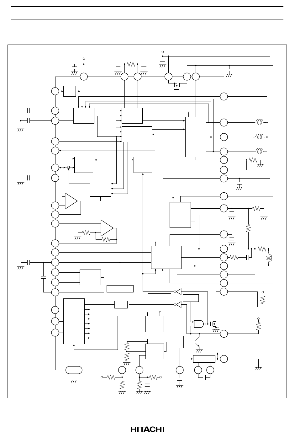
This COMBO driver for HDD application consists of sensorless spindle driver and BTL type VCM driver.
“PWM soft switching function” for low power dissipation and less commutation acoustic noise at the same
time is implemented by using the IPIC* process.
Note: I ntelligent P ower IC
Features
• PWM soft switching drive
• Small surface mount package: FP-48T
• Low thermal resistance: 30°C/W with 4 layer multi glass-epoxy board
• Low output on resistance
Spindle 1.2 Ω Typ
VCM 1.4 Ω Typ
• TTL compatible input level (with 3.3 V logic interface)
• High precision reference voltage output (for 3.3 V power supply)
Functions
• 16 bit serial port
• 2.0 A Max/3-phase spindle motor driver with PWM soft switch function
• 1.5 A Max BTL VCM driver with low crossover distortion
• PWMDAC for VCM drive current control
• Power off brake function for spindle motor
• Auto retract with constant output voltage
• Booster
• Internal Protector (OTSD, LVI)
• Precision power monitor
• OP amplifier

HA13614FH
Pin Arrangement
OP1OUT
OP1IN(−)
OP2IN(+)
Vss
OP2OUT
PC
TABGND
VCMPS
VCMN
Rs
VCMIN
VCMP
VCMSLC
POR
LVI1
DELAY
DACOUT
VREF
BC2
VIPWMH
Vpsv
VBST
48 47 46 45 44 43 42 41 40 39 3738
1
2
3
4
5
6
7
8
9
10
11
12
13 14 15 16 17 18 19 20 21 22 23 24
BC1
RETSET
RETPOW
TABGND
TABGND
VIPWML
12VGOOD
U
BRKDLY
DATA
SEENAB
V
RNF
SCLK
CLK
BRK
LVI2
36
COMM
35
PHASE
34
SPNCTL
33
UFLT
32
NFLT
31
VpsIN
30
VpsOUT
29
FLTOUT
28
Vpss
27
W
26
ISENSE
25
CT
TABGND
(Top View)
2

HA13614FH
Pin Description
Pin No. Pin Name Function
1 OP1OUT Output of OP amp. 1
2 OP1IN(–) Inverted input of OP amp. 1
3 OP2IN(+) Non-inverted input of OP amp. 2
4 Vss Power supply for +5 V
5 OP2OUT Output of OP amp. 2
6 PC External time costant connection terminal for phase compensation of VCM
driver
7 VCMPS Current sensing terminal for VCM driver
8 VCMN Output of VCM driver (Inverted output of VCMP)
9 Rs Current sensing terminal for VCM driver (differential input for VCMPS)
10 VCMIN Input of VCM driver (differential input for VREF)
11 VCMP Output of VCM driver (inverted output of VCMN)
12 VCMSLC External capacitor connection terminal for stabilizing internal reference
voltage of VCM driver
13 RETPOW Power supply terminal of retract driver
14 RETSET Output voltage set up terminal of retract driver
15 BC1 External capacitor connection terminal for pumping of booster
16 BC2
17 Vpsv +12 V power supply for VCM driver
18 VBST Output of booster circuit
19 BRKDLY Time constance set up terminal of delayed brake
20 U U-phase output of spindle motor driver
21 V V-phase output of spindle motor driver
22 RNF Current sensing terminal for spindle motor driver
23 BRK External capacitor connection terminal for power off brake
24 LVI2 Resistor connection terminal for set up the threshold of +3.3 V power monitor
25 CT Center tap connection terminal for spindle motor
26 ISENSE Input of PWM comparator
27 W W-phase output of spindle motor driver
28 Vpss +12 V power supply for spindle motor driver
29 FLTOUT PWMDAC output for current control of spindle motor driver
30 VpsOUT Output of power supply switch
31 VpsIN Input of power supply switch (+12 V)
32 NFLT Output of pre-filter for B-EMF sensing (capacitor connection terminal)
33 UFLT
3

HA13614FH
Pin Description (cont)
Pin No. Pin Name Function
34 SPNCTL PWMDAC input for current control of spindle motor driver
35 PHASE Toggle signal output for zero-crossing timing of B-EMF
36 COMM Commutation signal input for spindle motor driver during synchronous driving
37 CLK Master clock input of commutation logic circuit
38 SCLK Clock input of serial port for data strobe
39 SEENAB Enable signal input of serial port
40 DATA Data signal input of serial port
41 12VGOOD Output of power monitor for +12 V power supply (open drain)
42 VIPWML PWMDAC input for current control of VCM driver
43 VIPWMH
44 VREF Output of internal reference voltage
45 DACOUT PWMDAC output for current control of VCM driver
46 DELAY Capacitor connection terminal for set up the power on reset time
47 LVI1 Resistor connection terminal for set up the threshold of +12 V power monitor
48 POR Output of power on reset signal
TAB GND Ground of this IC
4

Block Diagram
C113
37
C101
UFLT
33
NFLT
FLTOUT
C1
SCLK
DATA
32
36COMM
35PHASE
SPN
GAIN
34
29
1.4V ref.
2
1OP1OUT
3OP2IN(+)
5OP2OUT
10VCMIN
VREF
44
VIPWMH
43
VIPWML
42
DACOUT
45
38
40
39
C102
SPNCTL
(TESTOUT)
C103
OP1IN(−)
C104
SEENAB
1
128
B-EMF
Amps
Input
OP Amp.1
+
−
Serial
input
RESET
Vss (+5V)
Vss
4
CLKCLK
filter
PWM
decoder
STANDBY
(+12V)
C112 C116
23
BRK
BRAKE
POR
OTSD
CLK
EXTCOM
Selector
Commutation
B-EMF
PWMOUT
MASK
TEST
OP Amp.2
+
−
Vref(=5.3V)
SPNENAB
EXTCOM
BRAKE
VCMENAB
SOFTSW
TEST
SPNGAIN
Vps
BIAS
LVI1 LVI2
47
R101 R107
R102 R108
R109
Brake
control
logic
19
BRKDLY
Current
control
(PWM)
VCMENAB
Vps Vss
Vss
24
Vps (+12V)
C111
VpsIN31VpsOUT
V
BST
+
VCM
driver
−
POW DWN
Power
monitor2
Power
monitor1
DELAY
Vdd
(+3.3V)
C117
30
V
V
BST
Retract
driver
P
N
OTSD
POR
delay
CLK
46
BC1 BC2
C105
28
BST
Spindle
driver
Booster
15 16TAB
Vpss
U
V
W
VCMSLC
VCMP
VCMN
VCMPS
C106
PC
V
Rs
BST
HA13614FH
C114
CT
25
U
20
V
21
W
27
RNF
22
ISENSE
26
Vpsv
17
RETPOW
13
RETSET
14
12
11
6
R104 C108
8
7
9
41
12VGOOD
(Open Drain)
POR
(L: RESET)
48
VBST
18
C115
C109
R
NF
C110
R106
R105
Vss (+5V)
Vss (+5V)
C107
R
S
R
R103
L
R110
5

HA13614FH
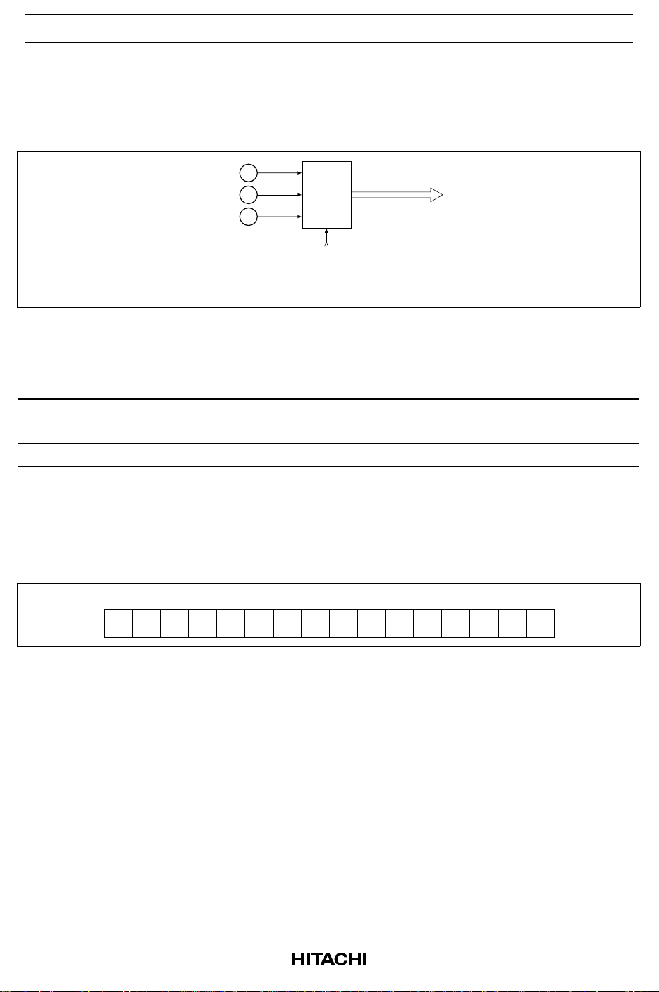
Serial Port
Construction
SEENAB
SCLK
DATA
Note: When POR = Low, internal RESET signal becomes High and when RESET = High,
all bit of serial port are set up default value as shown in table 2.
Serial
RESET *
port
D0 to D15
to each block
Figure 1 Construction of Serial Port
Table 1 Truth Table of Internal RESET Signal
Input Output Note
POR RESET
Low High 1
Open Low 1
Note: 1. When +5 V or +3.3 V power supply goes to Low, then POR = Low.
POR output is able to construct the wired logic with external signal.
Input Data
MSB LSB
D15 D14 D13 D12 D11 D10 D9 D8 D7 D6 D5 D4 D3 D2 D1 D0
Figure 2 Input Data
The serial port is required the 16 bits data (D0 to D15). When the data length is less than 16 bits, the
internal register will not be up dated. And when the data length is more than 16 bits, this register will take
later 16 bits and ignore the faster bit.
6

HA13614FH
Bit Assingnment
Table 2 Bit Assingnment of Serial Port
Bit Symbol 1 (= High) 0 (= Low) Default Note
D0 STANDBY Active Stand by 0 1
D1 VCMENAB VCM enable VCM disable 0 1
D2 SPNENAB Spindle enable Spindle disable 0 1
D3 BRAKE Brake enable Brake disable 0 1
D4 SENSEN B-EMF sense enable B-EMF sense disable 0 2
D5 VARCNT Variable count Normal count 0 2
D6 EXTCOM External commutation Internal commutation 0 2
D7 SRCTL1 High slew rate Low slew rate 0 3
D8 SRCTL2 Commutation time select (See table 4) 0 4
D9 SRCTL3 0 4
D10 OFFTIME1 Off time select of PWM drive (See table 5) 0 5
D11 OFFTIME2 0 5
D12 SPNGAIN High gain Low gain 0 6
D13 RETRACT Retract Not retract 0 1
D14 TEST1 For testing 0 7
D15 TEST2 0 7
Note: 1. The priority of operation for each bit is as shown in table 3.
2. This bit is using for start up of spindle motor. Please refer to the application note explained
about start up of spindle motor.
3. The slew rate during every commutation of spindle motor is selectable by using this bit. Please
select the suitable value of this bit for your motor.
4. This bit is used for setting up the commutation time (refer to figure 9) of spindle motor as shown
in table 4.
5. This bit is used for setting up the off time at PWM driving of spindle motor as shown in table 5.
6. The gain of current control for spindle motor is selectable by using this bit. Please select the
suitable value of this bit for your motor.
7. This bit will be used in fabrication test. Please set up D15 = “0” normally.
SPNCTL terminal (pin 35) is using for output terminal in the case of “1” for testing. Then please
do not input signal into pin 35 from outside.
7

HA13614FH
Table 3 Truth Table
Input Driver Output
OTSD 12VG OOD
Enable Low ×*
Disable Low ЧЧЧЧЧBraking Cut off On Cut off
Disable High Low ××××Braking Cut off Cut off Cut off
Disable High High 0 0 0 0 Cut off Cut off Cut off On
Disable High High 0 1 0 0 Braking Cut off Cut off On
Disable High High 1 × 0 0 On Cut off Cut off On
Disable High High 0 0 0 1 Cut off On Cut off O n
Disable High High 0 1 0 1 Braking On Cut off On
Disable High High 1 × 0 1 On On Cut off O n
Disable High High 0 0 1 × Cut off Cut off On On
Disable High High 0 1 1 × Braking Cut off On On
Disable High High 1 × 1 × On Cut off On On
1
*
Note: 1. The 12VGOOD terminal is open drain output type. The 12VGOOD signal output is determined by
the power monitor output for 12 V power supply, POR output and OTSD signal as shown in the
table below.
STAND BY SPNENAB BRAKE RETRACT VCMENAB Spindle
2
××××Braking Cut off On Cut off
Driver
VCM
Driver
Retract
Driver
Power
Switch
12 V Supply POR OTSD 12VGOOD
Cut off ××Low
× Low × Low
××Enable Low
Normal High Disable High
2. The symbol “×” means “Don’t care”.
Table 4 Commutation Time
SRCTL2 SRCTL3 Commutation Time (s)
0 0 24 × (128 / fclk)
0 1 16 × (128 / fclk)
1 0 12 × (128 / fclk)
1 1 No slew rate control
Note: The “fclk” is the frequency on pin “CLK”. (Recommendation: 20 MHz)
8
 Loading...