HIT 2SC1472 Datasheet

Application
High gain amplifier
Outline
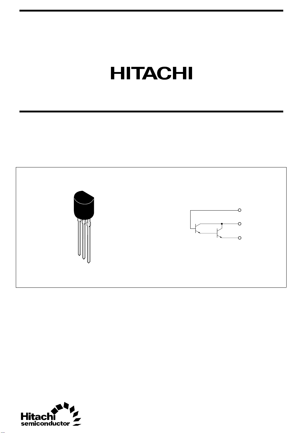
TO-92 (1)
2SC1472(K)
Silicon NPN Epitaxial, Darlington
3
2
1. Emitter
2. Collector
3. Base
3
2
1
1

2SC1472 (K)
Absolute Maximum Ratings (Ta = 25°C)
Item Symbol Ratings Unit
Collector to base voltage V
Collector to emitter voltage V
Emitter to base voltage V
Collector current I
Collector peak current i
Collector power dissipation P
CBO
CEO
EBO
C
C(peak)
C
Junction temperature Tj 150 °C
Storage temperature Tstg –55 to +150 °C
40 V
30 V
10 V
300 mA
500 mA
500 mW
2

2SC1472 (K)
Electrical Characteristics (Ta = 25°C)
Item Symbol Min Typ Max Unit Test conditions
Collector to emitter breakdown
V
(BR)CEO
voltage
Collector cutoff current I
Emitter cutoff current I
DC current transfer ratio h
Collector to emitter saturation
h
h
V
CBO
EBO
FE1
FE2
FE3
CE(sat)
voltage
Base to emitter voltage V
Gain bandwidth product f
BE(sat)
T
Collector output capacitance Cob — — 10 pF VCB = 10 V, IE = 0, f = 1 MHz
Turn on time t
Turn off time t
Storage time t
on
off
stg
Note: 1. The 2SC1472(K) is grouped by hFE as follows.
AB
h
FE1
h
FE2
h
FE3
2000 to 100000 5000 to 100000
3000 min 10000 min
3000 min 10000 min
30 — — V IC = 1 mA, RBE = ∞
— — 100 nA V
— — 100 nA V
1
*
2000 — 100000 IC = 10 mA, VCE = 5 V
1
*
3000 — — IC = 100 mA, VCE = 5 V
= 30 V, IE = 0
CB
= 10 V, IC = 0
EB
(Pulse Test)
1
*
3000 — — IC = 400 mA, VCE = 5 V
(Pulse Test)
— — 1.5 V IC = 100 mA, IB = 0.1 mA
— — 2.0 V IC = 100 mA, IB = 0.1 mA
50 — — MHz VCE = 5 V, IC = 10 mA
— 60 — ns VCC = 11 V
I
= 100 IB1 = 100 mA
C
I
= –I
B2
B1
— 800 — ns
— 350 — ns
P.G.
tr, tf ≤ 15 ns
PW ≥ 10 µs
duty ratio ≤ 10%
Switching Time Test Circuit
D.U.T.
6 k
6 k
0.002
50
0.002
+–
+–
50
50
–6 V
100
11 V
Unit R : Ω
CRT
C : µF
13 V
Input
0
Output
0
Response Waveform
10%
90%
10%
t
d
t
on
90%
t
stg
t
off
90%
10%
3
 Loading...