

Page 1

harman/kardon
BDS 2 / BDS 5 Service Manual
Page 1 of 63
IMPORTANT INFORMATION ABOUT PAIRING NEW LOADER
WITH MAIN BOARD ON PAGE 64-65.
harman/kardon Service Manual
HK BDS 2 / BDS 5
2 x 65W and 5 X 65w multi-voltage Blu-ray home cinema
receivers
OWNER’S MANUAL INTRODUCTION 2
BDS SYSTEM ACCESSORIES 3
FRONT
REMOTE C
TROUBLESHOOTING GUIDE
BASIC SPECIFICATIONS
FFFF
ADDEDFSF
Released EU2010 Harman Consumer Group, Inc. Rev 4, 03/2012
8500 Balboa Boulevard
Northridge, California 91329
AND REAR PANELS 4
ONTROL FUNCTIONS
9
RE UPGRADE PROCESS 10
CONTENTS
TROUBLESHOOTING CHARTS 11
EXPLODED VIEW AND PARTS 22
BDS 2 PA
6
8
BDS 5 PA
PCB DRAWINGS 25
WIRING DI
SCHE
RTS LIST 23
RTS LIST 24
AGRAM 33
MATIC DIAGRAMS
34-63 SOFTWA
Page 2
BDS
harman/kardon
BDS 2 / BDS 5 Service Manual
Page 2 of 63
Verify Line Voltage Before Using, Unpacking, Installation Location,
Cleaning, Moving the Receiver and Introduction
Introduction
Please register your product on our Web site at
www.harmankardon.com.
Note: You’ll need the product’s serial number.
At the same time, you can choose to be
notified about our new products and/or special
promotions.
Thank You for Choosing harman kardon® Products!
In the years since harman kardon engineers invented the high-fidelity receiver, we have
taken to heart this philosophy: Bringing the joy of home entertainment to as many people
as possible, adding performance and ease-of-use features that enhance the experience.
The BDS series of home entertainment systems offers a complete home entertainment
solution with a wealth of listening and viewing options in one sleek receiver. Each BDS
series system also includes a 5.1-channel, 2.1-channel or soundbar loudspeaker system,
a system remote control and all the cables and accessories you need to enjoy movies
and music in your own home, when you use them with your television or video display.
To get the maximum enjoyment from your new BDS system, we urge you to read this
manual thoroughly and refer back to it as you become more familiar with your new
system’s features and their operation.
If you have any questions about this product, its installation or its operation, please
contact your retailer or custom installer, or visit our Web site at www.harmankardon.com.
Verify Line Voltage Before Using
Your BDS receiver has been designed for use with 110 – 240-volt, 50Hz/60Hz AC current.
Your subwoofer has been designed for use with either 120-volt, 60Hz or 220 – 240-volt,
50/60Hz AC current, depending on where your system was sold. The receiver includes a
detachable IEC power cable designed for use in the region where the system is sold.
Connection to a line voltage other than that for which the units are intended can create
a safety and fire hazard and may damage the units. If you have any questions about
the voltage requirements for your specific model or about the line voltage in your area,
contact your dealer before plugging the unit into a wall outlet.
Unpacking
The carton and shipping materials used to protect your new player during shipment were
specially designed to cushion it from shock and vibration. We suggest that you save the
carton and packing materials for use in shipping if you move or if the unit ever needs
repair.
To minimize the size of the carton in storage, you may wish to flatten it. You can do it by
carefully slitting the tape seams on the carton’s bottom and collapsing it. You can store
cardboard inserts in the same manner. Packing materials that cannot be collapsed should
be saved along with the carton in a plastic bag.
If you do not wish to save the packaging materials, please note that the carton and
other sections of the shipping-protection materials are recyclable. Please respect the
environment and discard those materials at a local recycling center.
Remove the protective plastic film from the front-panel lens. Leaving the film in place will
affect the performance of your remote control.
Installation Location
• To ensure proper operation and to avoid the potential for safety hazards, place the
unit on a firm and level surface. When placing the unit on a shelf, be certain that the
shelf and any mounting hardware can support the weight of the product.
• Provide proper space both above and below the unit for ventilation. If this product will
be installed in a cabinet or other enclosed area, make certain that there is sufficient
air movement within the area. Under some circumstances, a fan may be required.
• Do not place the unit directly on a carpeted surface.
• Avoid installation in extremely hot or cold locations or in an area that is exposed to
direct sunlight or heating equipment.
• Avoid moist or humid locations.
• Do not obstruct the fan vents on the rear panel or the ventilation slots on the top and
sides of the unit or place objects directly over or next to them.
• Do not place the receiver directly on top of a product that generates excessive
heat.
• Due to the heat generated by the receiver and other components in your system,
there is the remote possibility that the rubber padding on the bottom of the unit’s
feet may leave marks on certain wood or wood-veneer materials. Use caution when
placing the unit on soft woods or other materials that heat or heavy objects may
damage. Some surface finishes may be particularly sensitive to absorbing such
marks, due to a variety of factors beyond harman kardon control, including the
nature of the finish, cleaning materials used, normal heat and vibration caused by
the use of the product, or other factors. Your warranty will not cover this type of
damage to furniture, so exercise caution in choosing an installation location for the
component and in performing normal maintenance practices.
• Your new harman kardon
connection for BD-Live™ interactivity.
®
Blu-ray Disc™ player requires a broadband Internet
Cleaning
Receiver
When the receiver gets dirty, wipe it with a clean, soft, dry cloth. If necessary, and only
after unplugging the AC power cord, wipe it with a soft cloth dampened with mild soapy
water, then a fresh cloth with clean water. Wipe it dry immediately with a dry cloth. NEVER
use benzene, aerosol cleaners, thinner, alcohol or any other volatile cleaning agent. Do
not use abrasive cleaners, as they may damage the finish of metal parts. Avoid spraying
insecticide near the unit.
Speakers and Subwoofer
When needed, use a soft cloth to remove any fingerprints or dust from the enclosures or
grilles. NOTE: Do not use any cleaning products or polishes on the enclosures or grilles.
Moving the Receiver
Before moving the receiver, disconnect any interconnection cords to other components,
and disconnect the unit from its AC outlet.
NOTE: The built-in Blu-ray Disc/DVD player in your BDS receiver is designed
and manufactured for compatibility with region management information that is
encoded on most Blu-ray Disc recordings and DVD recordings:
• BDS receivers sold in the USA are designed only for playback of discs
with Blu-Ray Disc Region Code A and DVD Region Code 1 information, or
for discs that do not contain any region code information.
• BDS receivers sold in Europe are designed only for playback of discs with
Blu-ray Disc Region Code B and DVD Region Code 2 information, or for
discs that do not contain region code information.
If there is a region code on a disc other than the one your BDS player is designed
for, it will not play in your BDS receiver.
3
Page 3
BDS
harman/kardon
BDS 2 / BDS 5 Service Manual
Page 3 of 63
System Components and Supplied Accessories
System Components
Your BDS system includes the following components:
BDS 800 System
1 x BDS 5 5.1-channel Blu-ray Disc receiver
4 x SAT-TS60 satellite speakers
1 x SAT-TS60 center speaker
1 x HKTS200SUB powered subwoofer
BDS 700 System
1 x BDS 5 5.1-channel Blu-ray Disc receiver
4 x SAT-TS7 satellite speakers
1 x CEN-TS7 center speaker
1 x HKTS200SUB powered subwoofer
BDS 600 System
1 x BDS 5 5.1-channel Blu-ray Disc receiver
1 x SB10 soundbar speaker
1 x HKTS210SUB powered subwoofer
BDS 400 System
1 x BDS 2 2.1-channel Blu-ray Disc receiver
2 x SAT-TS60 satellite speakers
1 x HKTS200SUB powered subwoofer
BDS 300 System
1 x BDS 2 2.1-channel Blu-ray Disc receiver
2 x SAT-TS11 satellite speakers
1 x HKTS200SUB powered subwoofer
Supplied Accessories
If any of these items are missing, please contact harman kardon Customer Service via
www.harmankardon.com.
BDS 800, BDS 400 Systems
System
remote
control
EJECT POWER TV
iPOD
RADIO
DISC
A - B
REPEAT
SETTINGS
2
1
5
4
8
7
0
CLEAR
SURROUND
OPTIONS
HOME
OK
EXIT
POP-UP
TOP MENU
+ +
VOLUME
CHANNEL
MUTE
PROGRAM
BOOKMARK
THUMBNAIL
HDMI™ cable
AUX
DISPLAY
3
6
9
FIND
––
ZOOM
FM wire antenna
Two 5-meter (16.4-foot)
speaker cables – red and
white color bands
Satellite speaker
wall-mount brackets
(four with BDS 800
system, two with
BDS 400 system)
BDS 700, BDS 300 Systems
System
remote
control
EJECT POWER TV
iPOD
RADIO
AUX
DISC
A - B
REPEAT
DISPLAY
SETTINGS
2
1
3
5
6
4
8
9
7
0
FIND
CLEAR
SURROUND
OPTIONS
HOME
OK
EXIT
POP-UP
TOP MENU
+ +
VOLUME
CHANNEL
MUTE
––
PROGRAM
ZOOM
BOOKMARK
THUMBNAIL
One 4-meter (13.1-foot) speaker
cable for center speaker – green
color band (BDS 700 system only)
One mono RCA audio cable for
connection to the subwoofer –
purple connectors
BDS 600 System
System
remote
control
EJECT POWER TV
iPOD
RADIO
DISC
A - B
REPEAT
SETTINGS
2
1
5
4
8
7
0
CLEAR
SURROUND
OPTIONS
HOME
OK
EXIT
POP-UP
TOP MENU
+ +
VOLUME
CHANNEL
MUTE
PROGRAM
BOOKMARK
THUMBNAIL
AUX
DISPLAY
3
6
9
FIND
––
ZOOM
Two soundbar wallmount brackets
Two rubber feet
HDMI cable
FM wire antenna
Two 5-meter (16.4-foot)
speaker cables – red and
white color bands
Two 10-meter (32.8-foot) speaker cables
for rear satellites – gray and blue color
bands (BDS 700 system only)
Satellite speaker wallmount brackets and
hardware (four with
BDS 700 system, two
with BDS 300 system)
One center speaker
wall-mount bracket
(BDS 700 system only)
HDMI cable
FM wire antenna
Three speaker cables
Center speaker wallmount bracket (BDS
800 system only)
One mono RCA audio cable for
connection to the subwoofer –
purple connectors
4
One 4-meter (13.1-foot)
speaker cable for center
speaker – green color band
(BDS 800 system only)
Two 10-meter (32.8-foot) speaker cables
for rear satellites – gray and blue color
bands (BDS 800 system only)
Metal stop plates
and screws for
satellite speaker
wall-mount
brackets (four
with BDS 800
system, two with
BDS 400 system)
One mono RCA audio cable for
connection to the subwoofer –
purple connectors
Page 4
BDS
harman/kardon
BDS 2 / BDS 5 Service Manual
Page 4 of 63
Receiver Front-Panel Controls
Receiver Front-Panel Controls
Disc Slot Information Display
Disc Slot: Insert a compatible disc into the slot. The BDS receiver’s disc player will
accept 5-inch (12cm) and 3-inch (8cm) discs.
Information Display: Various messages appear on this display in response to
commands and to show the audio/video that is playing, the settings or other aspects
of the BDS receiver’s status as described throughout this manual.
Eject Button (on top of unit): Press this button to eject a disc from the BDS
receiver’s built-in disc player. Before pressing this button, make sure no objects are
blocking the disc-slot opening. NOTE: If you do not remove the ejected disc within
90 seconds, it will automatically re-load back into the disc player for protection.
Standby Button (on top of unit): This button toggles the receiver between the On
and Standby modes.
Power Indicator: This LED surrounds the Standby button. When the BDS receiver
is plugged into AC power, the LED turns amber to indicate that the receiver is in
Standby mode (ready to be turned on). When you turn the BDS receiver on (by the
Standby button or the remote control’s Power button), the LED turns white.
Headphone Jack: Insert the 3.5mm stereo mini connector from a set of headphones
Eject Button
(on top panel)
Headphone Jack
into this jack. NOTE: When a plug is inserted into the Headphone jack, the BDS
receiver’s speaker outputs automatically mute; the HDMI audio output remains
active.
Volume Control: Rotate the disc clockwise to raise the volume; rotate
counterclockwise to lower the volume. The volume level will appear on the
Information Display and on the on-screen menu.
IMPORTANT: Do not turn the receiver’s Volume control up to or past the point
where the audio from the speakers becomes distorted. Doing so can damage the
speakers.
USB 2.0 Port: Gently insert a flash drive or HDD disk drive with a USB Standard-A
cable to this port.
IMPORTANT: Do not connect a PC or other USB host/controller to this port, or
you may damage both the BDS receiver and the other device.
Orient the device’s plug so it fits all the way into the BDS receiver’s USB connector.
You may insert or remove the device at any time – there is no installation or ejection
procedure.
Standby Button
(on top panel)
USB Port
Volume Control
5
Page 5
BDS
harman/kardon
BDS 2 / BDS 5 Service Manual
Page 5 of 63
Receiver Rear-Panel Connections
Receiver Rear-Panel Connections
Main Power Switch Speaker Connectors (BDS 5 Shown)
AC Power Connector
NOTE: See the Connections section, on page 14, for detailed information about
making connections.
AC Power Connector: After you have made and verified all other connections, plug
the supplied AC power cord into this input and into an unswitched AC outlet.
Main Power Switch: This mechanical switch turns the BDS receiver’s power supply
on or off. After you have made and verified all connections (see the Connections
section, on page 14), set this switch in the On position. During normal use you will
usually leave this switch set to On; it cannot be turned on or off using the remote
control. To conserve energy when you’re not going to be using the receiver for an
extended period of time, set this switch to Off.
Speaker Connectors: Use the speaker wires supplied with the speakers to connect
the satellite and center speakers to the proper terminals.
•
The BDS 5 receiver (shown) has connections for five speakers: front left, front
right, surround left, surround right and center.
•
The BDS 2 receiver (not shown) has connections for two speakers: front left
and front right.
See Connections, on page 14, for more information.
Subwoofer Output: Use the supplied mono RCA audio cable (with the purple
connectors) to connect this jack to the subwoofer’s Line-Level In LFE jack.
See Connecting the Subwoofer, on page 16, for more details about making
connections.
BD-Live Connector: To be able to use the BD-Live feature, connect this port to your
local area network (LAN) using a Cat. 5/Cat. 5e/RJ-45 network cable. See BD-Live
Interactivity, on page 25, for details.
Cooling Fan Air Exhaust Optical
BD-Live Connector
Digital
Inputs
Subwoofer
Output
Optical Digital Inputs: Connect the optical digital output of an audio-only source
component here. The signal may be a Dolby
a standard PCM digital-audio bitstream.
NOTE: Use only one type of digital connection for each source component.
Coaxial Digital Input: Connect the coaxial digital output of an audio-only source
component here. The signal may be a Dolby Digital bitstream, a DTS bitstream or a
standard PCM digital-audio bitstream.
NOTE: Use only one type of digital connection for each source component.
HDMI Output (HDMI ver. 1.3a): Connect the BDS receiver’s HDMI output to your
TV’s HDMI input. Since the HDMI cable transmits both video and audio to the TV, we
recommend that you set the receiver’s HDMI audio output to Off in the receiver’s
Audio menu to take full advantage of your BDS system’s superior audio performance.
See Audio Settings, on page 21, for more information.
IMPORTANT: Your BDS receiver is in compliance with HDCP (High-Definition Copy
Protection). Your TV must also be HDCP-compliant to be used with the BDS receiver’s
HDMI output. For best results, we do not recommend HDMI connections in excess of
ten feet (about 3 meters) without a repeater. If your TV has a DVI input, you may use
an optional HDMI-to-DVI cable or adapter for the video connection to the TV. (The
DVI connection is video-only.)
Analog Audio Inputs 1 and 2: Use these inputs to connect to an audio-only source
component (such as a tape deck). Do not connect a turntable to these jacks without
a phono preamp.
The Bridge IIIP Connector: Connect The Bridge IIIP iPod/iPhone dock (available
separately) to this terminal.
FM Antenna Connector: Connect the supplied FM antenna to this terminal.
HDMI Output
Coaxial
Digital Input
Analog
Audio
Inputs
The Bridge IIIP
Connector
®
Digital bitstream, a DTS® bitstream or
FM Antenna Connector
6
Page 6
BDS
harman/kardon
BDS 2 / BDS 5 Service Manual
Page 6 of 63
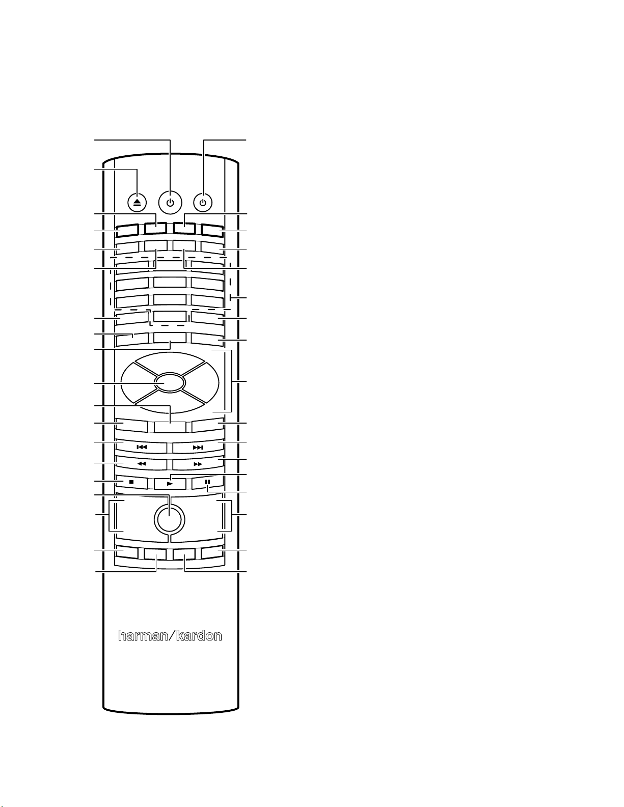
Remote Control Functions
Remote Control Functions
Power Button
Eject Button
EJECT POWER TV
Radio Button
RADIO
Disc Button
Settings Button
Repeat Button
Clear Button
Home Button
Surround Button
OK Button
Top Menu Button
Exit Button
Previous/Step
Button
Search/Slow
Reverse Button
Stop Button
Mute Button
Volume Up/Down
Buttons
Program (Red)
Button
Bookmark
(Green) Button
DISC
REPEAT
SETTINGS
1
4
7
CLEAR
EXIT
SURROUND
TOP MENU
HOME
+ +
VOLUME
PROGRAM
BOOKMARK
2
5
8
0
OK
MUTE
iPOD
A - B
THUMBNAIL
DISPLAY
3
6
9
FIND
OPTIONS
POP-UP
CHANNEL
––
AUX
ZOOM
TV Power Button
iPod Button
Aux Button
Display Button
A-B Button
Numeric Buttons
Find Button
Options Button
Cursor Controls
Pop-Up Menu
Button
Next/Step Button
Search/Slow
Forward Button
Play Button
Pause Button
Channel Up/
Down Buttons
Zoom (Blue)
Button
Thumbnail
(Yellow) Button
Eject Button: Press this button to eject a disc from the BDS receiver’s built-in disc
player. Before pressing this button, make sure no objects are blocking the disc slot
opening.
Power Button: Pressing this button toggles the BDS receiver between the On and
Standby modes.
TV Power Button: After you program the remote control, pressing this button turns
the TV’s power on and off. See Programming the Remote, on page 18.
Disc Button: Pressing this button selects the BDS receiver’s built-in disc player as
the system’s active audio and video source and plays a disc that has been inserted
into the player. Pressing this button also puts the remote control into the disc player
control mode. See Using the Disc Player, on page 23, for details. NOTE: Pressing this
button when the BDS receiver is in the Standby mode will switch it on.
Radio Button: Pressing this button selects the BDS receiver’s built-in FM radio as
the system’s active audio source. Pressing this button also puts the remote control
into the control mode for the radio. See Using the Radio, on page 26, for details.
NOTE: Pressing this button when the BDS receiver is in the Standby mode will
switch it on.
iPod Button: Pressing this butt on s elect s an iPo d inse rted in a conn ected
The Bridge IIIP dock (available separately) as the system’s active audio source.
Pressing this button also puts the remote control into the control mode for the iPod.
See Listening to Your iPod/iPhone, on page 25, for details. NOTE: Pressing this
button when the BDS receiver is in the Standby mode will switch it on.
Aux Button: Pressing this button selects the receiver’s active rear-panel audio input
as the system’s active audio source. Repeatedly pressing the button cycles through
all of the rear-panel audio inputs. See Listening to Audio Sources, on page 26, for
details.
Pressing this button also places the remote into the auxiliary-component control
mode, enabling the remote to use any pre-programmed and/or learned functions.
See Listening to Audio Sources, on page 26, for details. NOTE: Pressing this button
when the BDS receiver is in the Standby mode will switch it on.
Settings Button: Pressing this button displays the BDS receiver’s Settings menu.
See Settings Menus, on page 20, for details.
Repeat Button: When the BDS is playing a Blu-ray Disc recording or DVD, pressing
this button cycles through the following repeat modes: Chapter, Title, All, Off. When
the BDS is playing a CD or listening to media stored on an iPod or USB device, this
button cycles through the following repeat modes: Track, All, Off.
A-B Button: Pressing this button activates the A-B repeat mode. The first press sets
the “A” repeat point; the second press sets the “B” repeat point and begins repeating
the section of the program between the two points. Pressing the A-B button while
the A-B repeat mode is active cancels the A-B repeat mode. This feature works both
for the built-in disc player and for content from a USB device. Note: This feature is
disc-dependent. Some discs do not allow A-B repeat.
Display Button: When playing Blu-ray Disc and DVD recordings, pressing this
button activates a bar display containing information about the currently-playing
disc or program. The button does not function when the BDS is playing material from
an iPod, a USB device, an auxiliary source or the radio.
Numeric Buttons: Use these buttons to enter numbers for various items.
Clear Button: This button clears an incorrect entry made using the Numeric
buttons.
Find Button: Pressing this button during disc playback activates the search function,
allowing you to jump to a specific location on the disc. You can find a location by
title, chapter or time. Note: This feature is disc-dependent. Some discs do not allow
finding locations by title.
Home Button: Pressing this button returns the on-screen display to the Home
screen from whatever screen is active when the button is pressed.
8
Page 7

BDS
harman/kardon
BDS 2 / BDS 5 Service Manual
Page 7 of 63
Remote Control Functions
Surround Button: Pressing this button cycles through all of the surround-sound
modes that are available for the active program. Each press of the Surround button
will change to the next mode in line. A pop-up display will appear, showing the
modes as you cycle through them. NOTE: Not all surround modes will be available
for all programs. See Surround-Sound Modes, on page 23, for more information.
Options Button: Pressing this button displays any available options for the item
that is active at the time the button is pressed. When listening to an Aux source,
pressing the Options button lets you adjust the audio delay to eliminate “lip sync”
errors between the sound and picture when watching video programs with sound
playing through one of the receiver’s rear-panel audio inputs. See Listening to Audio
Sources, on page 26, for details.
Cursor Controls: Use these buttons to navigate through items on the on-screen
menu.
OK Button: Press this button to select the highlighted item on the on-screen menu.
Exit Button: Pressing this button exits the current on-screen menu and displays the
previous screen.
Top Menu Button: Displays the top menu of the Blu-ray Disc recording or DVD that
is playing. NOTE: This feature is disc-dependent. Not all DVDs have top menus. If
the DVD has no top menu, pressing the Top Menu button may display the disc menu,
depending on how the disc’s menu system was authored. See Using the Disc Player,
on page 23, for details.
Pop-Up Button: Pressing this button while playing a Blu-ray Disc recording or DVD
displays its disc menu. NOTE: This feature is disc-dependent. Not all DVDs have
pop-up menus. If the DVD has no pop-up menu, pressing the Pop-Up button may
display the disc menu, depending on how the disc’s menu system was authored.
Previous/Step Button: Press this button once to skip to the beginning of a track
or, when viewing photos, to the previous photo. Press the button twice to skip to
the beginning of the previous track. Press the button repeatedly to go back through
the previous chapters or tracks. When video content is playing on Blu-ray Disc
recordings and DVDs, press the Pause button first; afterwards, each subsequent
press of the Previous/Step button reverses the video one frame.
Next/Step Button: Press this button once to skip to the beginning of the next track
or, when viewing photos, to the next photo. Press the button repeatedly to advance
through the next chapters or tracks. When video content is playing, press the Pause
button first; afterwards, each subsequent press of the Next/Step button advances
the video one frame.
Search/Slow Reverse Button: Press this button to reverse through a disc track.
For Blu-ray Disc recordings and DVDs, each press cycles through 2x, 4x, 8x, 16x
and 32x reverse speed. Pressing the button while a Blu-ray Disc recording or DVD is
paused will reverse through the chapter in slow motion. Each press cycles through
1/2, 1/4, 1/8 and 1/16 normal speed.
Search/Slow Forward Button: Press this button to fast-forward through the current
disc track. For Blu-ray Disc recordings and DVDs, each press cycles through 2x, 4x,
8x, 16x and 32x normal speed. Pressing the button while a Blu-ray Disc recording
or DVD is paused will play through the chapter in slow motion. Each press cycles
through 1/2, 1/4, 1/8 and 1/16 normal speed.
Stop Button: Press this button to stop playback at the current point. (Pressing the
Play button will resume playback from this point.) Press the Stop button twice to
stop playback fully. NOTE: Some settings and functions will be available only when
the player is fully stopped.
Play Button: Press this button to play a disc that has been loaded into the player’s
disc drawer or a music file that has been highlighted on the on-screen menu.
Pressing this button when viewing photos begins a slide show of all photos in the
current folder.
Pause Button: Press this button to pause a disc or music file that is playing. Pressing
the button while a Blu-ray Disc recording or DVD is playing will freeze-frame on the
current video frame. Pressing the button while the disc is paused will resume play.
Pressing this button while viewing photos freezes the current photo on the screen.
Volume +/– Buttons: Press these buttons to increase or decrease the volume of the
BDS receiver’s speaker outputs. NOTE: The Volume +/– buttons do not change the
volume of the HDMI audio outputs.
IMPORTANT: Do not turn the Volume buttons up to or past the point where the
audio from the speakers becomes distorted. Doing so can damage the speakers.
Mute Button: Press this button to mute the sound from the BDS receiver’s speaker
outputs. Press the button again to un-mute the sound. NOTE: The Mute button does
not mute the HDMI audio outputs.
Channel +/– Buttons: When Radio is the source selected on the remote control, the
Channel +/– buttons select the next higher or lower preset station.
Bookmark (Green) Button: Press this button to activate the Bookmark function.
See Bookmark Function, on page 24, for more information.
Thumbnail (Yellow) Button: Press this button while playing a photo slide show to
display thumbnail images of all photos in the slide show.
Program (Red) Button: Press this button to create a programmed playback
list for the currently-playing disc. See Programmed Play, on page 25, for more
information.
Zoom (Blue) Button: Press the Zoom button to zoom in on or recede from a video
image or slide. Use the Navigation buttons to zoom in on different sections of the
image. NOTE: This function is disc-dependent for Blu-ray Disc recordings and DVDs.
Not all discs can be zoomed in on.
Red, Green, Yellow and Blue Buttons: When the BDS is playing a Blu-ray Disc
recording, these buttons can activate features and menus that may vary from disc
to disc. Refer to the menu instructions for each particular disc for more information.
NOTE: These Blu-ray Disc functions may override the Bookmark, Thumbnail,
Program and Zoom functions.
9
Page 8

BDS
harman/kardon
BDS 2 / BDS 5 Service Manual
Page 8 of 63
Troubleshooting
If your BDS system isn’t performing the way you think it should, check to see if the problem is
covered in this section before calling your dealer or contacting a harman kardon representative.
Problem Solution
Troubleshooting
The receiver won’t power up (the Power indicator is not lit): • Check that the receiver’s Power cord is properly plugged into the receiver’s AC
Sound plays through the BDS system speakers, but there is no TV picture: • Check the HDMI connection between the receiver and the TV.
There is no sound coming from just the subwoofer: • Check that the subwoofer’s Power cord is plugged into a working AC outlet.
There is a constant hum in the sound: • Check that all input cables are plugged all the way into their connectors.
The disc does not play: • Check that the disc is inserted correctly (label side up).
There is noise or other interference in the picture while playing a Blu-ray Disc recording
or DVD:
The sound and picture are out of sync when listening to an Aux source: • Press the Options button and perform the Lip Sync adjustment to bring the sound
Cannot tune in radio stations: • Check that the FM antenna is correctly connected.
The receiver does not respond to remote-control commands: • Replace all three remote-control batteries with fresh ones, and make sure that they
The remote does not control programmed components (TV or video): • Check that you have pressed the remote’s Aux button before trying to operate the
The Ø symbol appears on the screen when you press a remote-control button: • The selected function is not permitted at the time the button is pressed.
The receiver does not respond to commands, or it behaves in an erratic way: • Unplug the receiver’s Power cord from the AC outlet, wait 30 seconds, then plug
You can find additional troubleshooting information in the FAQs link on the Support page at www.harmankardon.com.
Power Input connector.
• Check that the Power cord is plugged into a working AC outlet. If the outlet is
controlled by a switch, make sure the switch is set in the “On” position.
• Check that the receiver’s Main Power switch (located on the rear panel) is in the
“On” position.
• Check that the TV is turned on and is set to the proper input source.
• Unplug the HDMI cable from the TV and plug it back in again.
• Check that the subwoofer’s Power switch is in the “On” position.
• Check that the Subwoofer Level control is not turned all the way down (fully
counterclockwise).
• Check that the audio connection between the receiver and the subwoofer has been
properly made.
• Check the receiver’s Settings: Configuration menu to make sure that the subwoofer
volume has not been set at –10dB.
• Check that all cables are at least 10 ft (3.3m) from fluorescent lights.
• Check that all cable connectors are clean. If necessary, wipe them with a cloth
slightly moistened with alcohol.
• Set the subwoofer’s Power switch to “Off.” If the hum goes away, there is a ground
loop between the subwoofer and the receiver. Plugging the subwoofer’s Power cord
into the same AC outlet that the receiver is plugged into should eliminate the ground
loop.
• Check that the disc is the correct type: BD-Video (single-layer or double-layer),
DVD-Video, DVD+R/+RW, DVD-R/-RW, CDDA (CD digital audio), CD-R/RW. Other
disc types will not play.
• Check that the disc surface is clean and not scratched.
• Check that the disc surface is clean and not scratched.
and picture into synchronization.
• Adjust the antenna’s position. If necessary, use a powered FM antenna or an
outdoor FM antenna.
are installed with the correct polarity.
• Hold the remote closer to the receiver.
• Check that the receiver’s remote sensor is in the line of sight of the remote control.
component.
• Re-program and/or re-teach the component’s commands into the remote.
it back in.
29
Page 9

BDS
harman/kardon
BDS 2 / BDS 5 Service Manual
Page 9 of 63
Specifications
Specifications
BDS 5 receiver (BDS 800, BDS 700, BDS 600 systems)
BDS 2 receiver (BDS 400, BDS 300 systems)
Audio Section
Continuous average power, stereo mode (BDS 5, BDS 2): 65 watts per channel, 20Hz – 20kHz, @ <0.1% THD, both channels driven into 6 ohms
Multichannel power (BDS 5 only): 65 watts per channel, 20Hz – 20kHz, @ <0.1% THD, into 6 ohms
Input sensitivity/impedance (line inputs): 250mV/46k ohms
Signal-to-noise ratio (IHF-A): –90dB
Frequency response @ 1W (±0.5dB): 20Hz – 20kHz
Slew rate: 40V/µsec
FM Tuner Section
Frequency range: 87.5MHz – 108.0MHz (US and EU)
Usable sensitivity IHF: >14dBf
Signal-to-noise ratio (mono/stereo): –60dB/–55dB
Distortion (mono/stereo): 0.3%/0.5%
Stereo separation: –45dB @ 1kHz
Image rejection: –70dB
IF rejection: –80dB
Disc Player Section
Supported disc formats: 5-inch (12cm) or 3-inch (8cm) BD-Video (single-layer or double-layer), DVD-Video, DVD+R/+RW,
Region code (BD/DVD): A/1 (USA); B/2 (EU)
Audio formats: Dolby Digital, Dolby Digital Plus, Dolby TrueHD, DTS Digital, DTS-HD High Resolution Audio, DTS-HD
Still-image format: JPEG
Video signal system: NTSC (USA) or PAL (EU)
Frequency response: 20Hz – 20kHz ±0.5dB
Signal-to-noise ratio: –90dB (A-weighted)
Dynamic range: 90dB (16-bit)
THD @ 1kHz (DVD/CD): 0.1%
Wow & flutter: Below measurable limits
DVD-R/-RW, CDDA (CD digital audio), CD-R/RW discs
Master Audio, PCM, WMA (DRM-free version only): WMA9, CBR @ 192kbps, VBR @ 355kbps; MP3:
32kbps – 320kbps bitrates, including variable-bitrate encoding
Video Section
Television format: NTSC or PAL (selectable)
HDMI version: 1.3a, with 30/36-bit Deep Color
General
Power requirement: 110 – 240V AC, 50/60Hz
Power consumption: 110W maximum (BDS 5), 70W maximum (BDS 2); <1W standby
Dimensions (H x W x D): 4" x 15-25/32" x 10-1/4" (102mm x 401mm x 260mm)
Weight: 14.3 lb (6.5kg) (BDS 5); 14 lb (6.4kg) (BDS 2)
Depth measurement does not include terminal connections. Height measurement includes feet and chassis.
35
Page 10

4-1
harman/kardon
BDS 2 / BDS 5 Service Manual
Page 10 of 63
Software upgrade
Preparation to upgrade software
1) Power on and press "SETTINGS" button and ‘Left’ button on the remote control to check the SW
version info .
2) Select an match upgrade package by the SW version info, for example ,
BDS2_EU VX.XX.XX, you must select the package HK_BDS2_EU_VX.XX.XX
3) Unzip the package, and copy the ‘UPG’ folder to the root folder in an USB disc
4) Start the CD Burning software and create a new CD project (Data Disc) .
5) Burn the UPG folder onto a blank CDR.
A. Procedure for software upgrade:
A) Upgrade software via USB Flash Drive:
1) plug in the Preparation step 3) mentioned USB disc
2) Power on and press "SETTINGS" button, invoke the Settings menu
3) navigate to General Settins-> ‘System’ -> System Upgrade -> USB
4) press ‘OK” to start upgrade.
5) it will reboot when upgrade successful (about 2Min).
B) Upgrade software via CDR
1) insert the upgrade CD.
2) Power on and press "SETTINGS" button, invoke the Settings menu
3) navigate to General Settins-> ‘System’ -> System Upgrade -> Disc
4) press ‘OK” to start upgrade.
5) it will reboot when upgrade successful (about 5Min).
B. Upgrading Procedure
C. &onfirmXpgradH
1,press "SETTINGS" button and ‘Left’ button on the remote control to check the new SW version info
and confirm the upgrade.
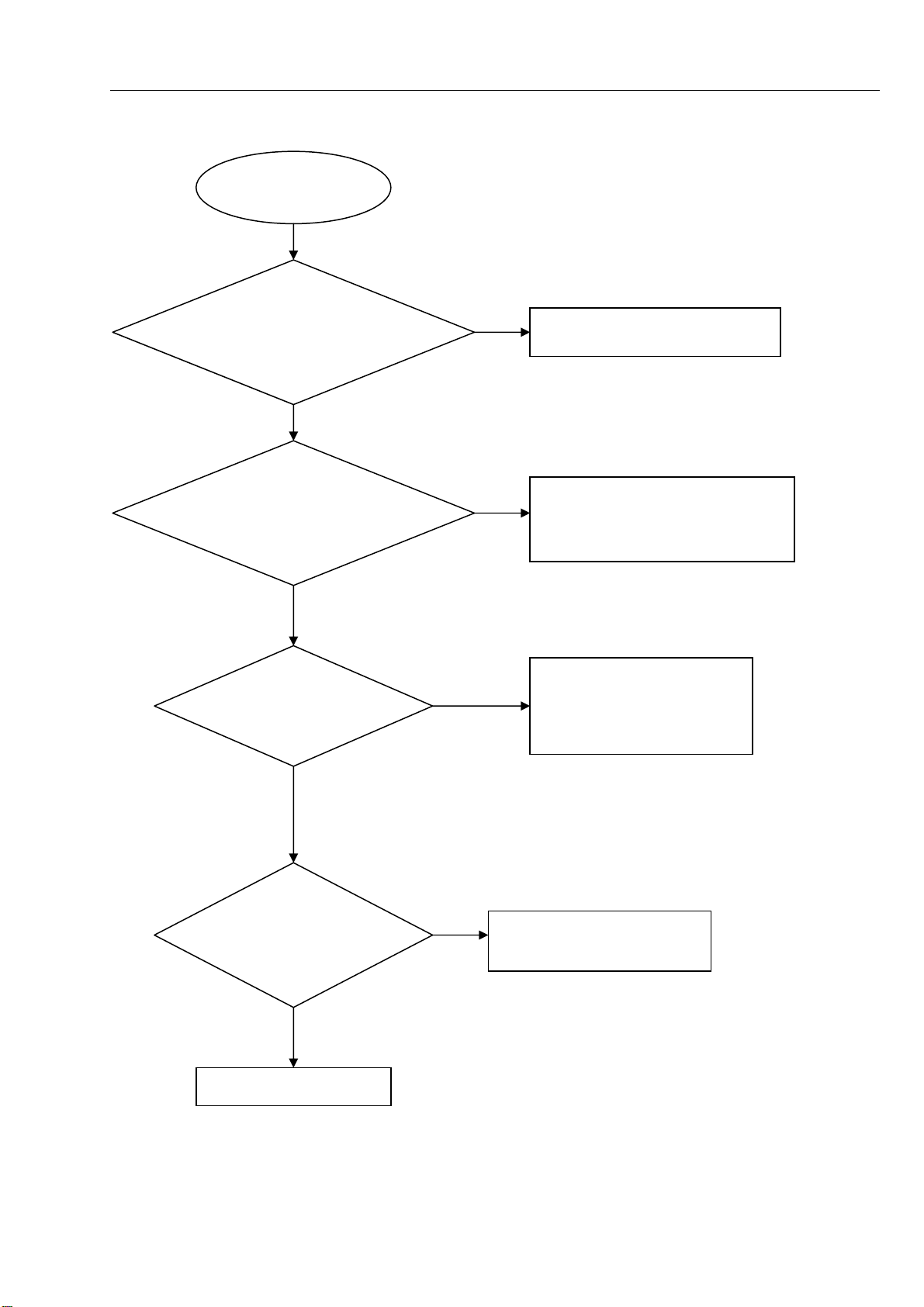
Page 11
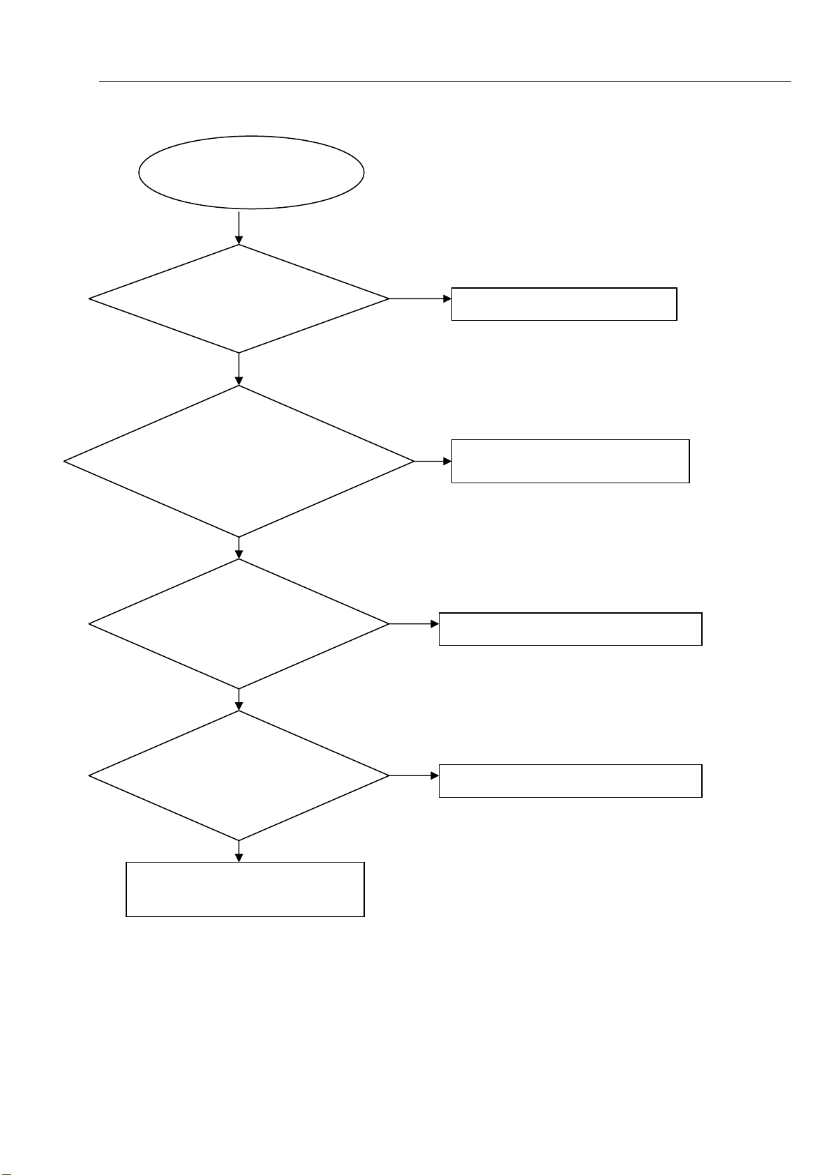
Power on led doesn't work
harman/kardon
BDS 2 / BDS 5 Service Manual
Page 11 of 63
power on led doesn't work
GO
5-1 Trouble shooting Chart
Switch performance
check
OK
NG
change switch
Check the cable XS603 is
NG
connect well to power board
CN501
OK
Reconnect the cable
Check+5V,+12V,+5VSTB
voltage on the power and
front board
NG
Refer to Power supply board part
OK
Check the power on led
control circuit is OK
OK
Replace the LED610,LED611
NG
Replace the FB
Page 12
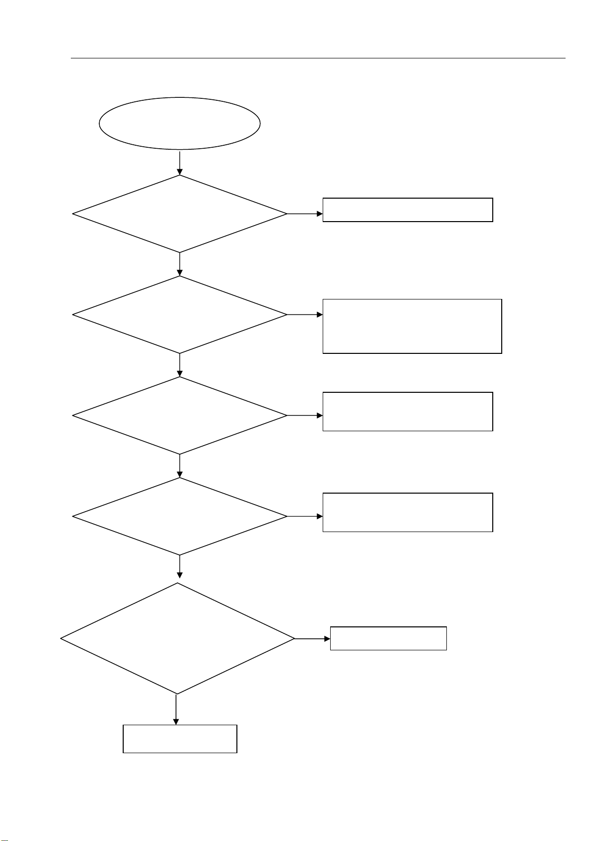
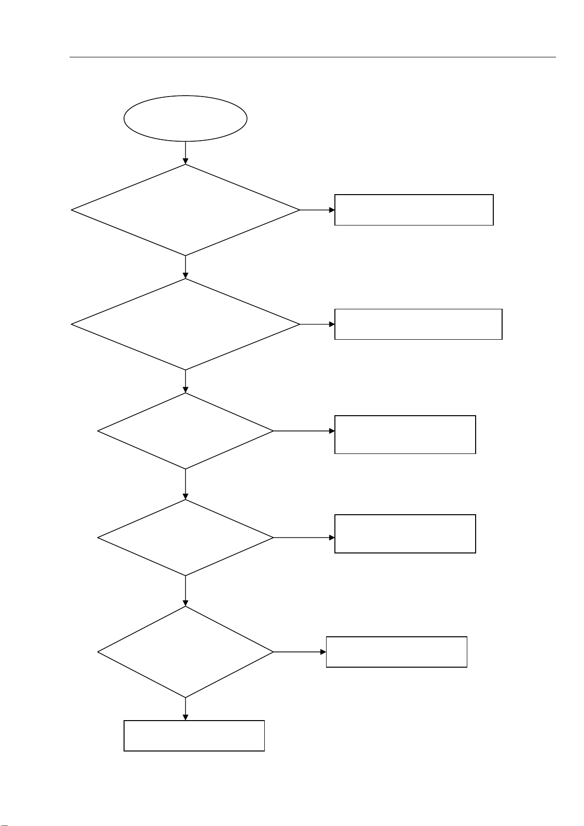
No display on VFD
harman/kardon
BDS 2 / BDS 5 Service Manual
Page 12 of 63
No display on VFD
5-2 Trouble shooting Chart
Go
Check every supply
voltage on AM board is
normal
Yes
Check+5V,+12V,+5VSTB
voltage on the power and
front board
Yes
Check the power key is
working normally
Yes
No
No
No
Refer to Power supply board part
Fix the connection XS603 on front board
and CN501 on power board, and 20pin
FFC cable from FB to AM board
Replace U721 on AM board, or replace
the AM board
Check the front board
signals VDIN,VCLK,
VSTB
Yes
1.Check whether bad
solder exists on pins of
VFD,
Yes
Replace VFD or FB
No
Check the U601 pin 31,32,34 arrive the
condition XP808 13,10,9
No
Correct connection
Page 13
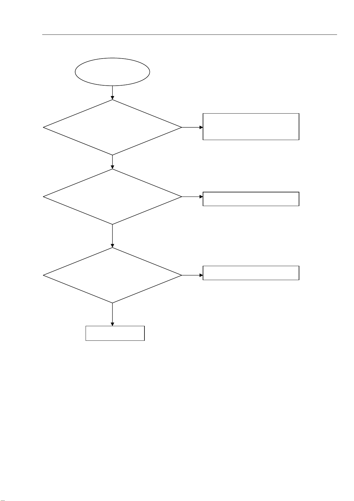
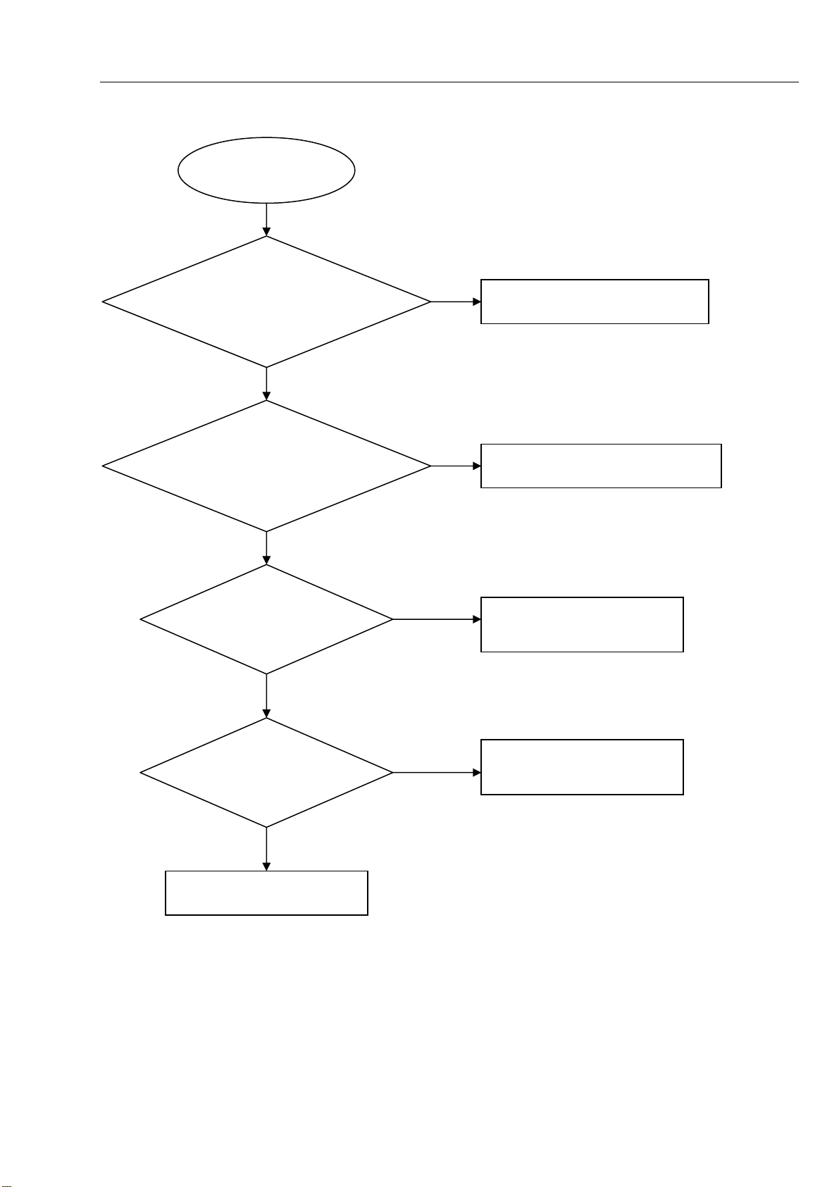
Remote control does not work
harman/kardon
BDS 2 / BDS 5 Service Manual
Page 13 of 63
Remote control
does not work
Go
5-3 Trouble shooting Chart
Check whether the remote
controller’s battery is
exhausted or not.
Yes
Check the 2pin FFC cable
from AM to BD board is
connect wenll
Yes
Check the IR601 power
supply is OK, IR1’3 is about
3.3V
No
No
No
Replace the battery for remote
controller
Reconnect the cable
Check the +3.3V net on front board
Yes
Replace IR1
Page 14
Can’t read disc or can’t eject
r
harman/kardon
BDS 2 / BDS 5 Service Manual
Page 14 of 63
Can’t read disc or can’t
eject
GO
5-4 Trouble shooting Chart
Check whether the
DVD loader running is
normal
Yes
Check 45pin and 8pin
cable from BD board
connection to the loader is
normal
Yes
Replace the loade
NO
Check the connection 4pin cable from the
BD board
NO
Fix the connection the 45pin cable
Page 15
5.1/2.1 channel no audio output
p
harman/kardon
BDS 2 / BDS 5 Service Manual
Page 15 of 63
5.1/2.1 channel no audio
ut
out
Go
5-5 Trouble shooting Chart
Check the 10pin/4pin cable is
connect well from AM to JC
board
Yes
Check XP701 is short
to GND
No
Check +32V at XP702 on
AM board is OK
No
Reconnect well
Yes
Replace the AM board
No
Refer to Power supply board
Yes
check the system weather is
ear mode or not, pull out the
4pin cable XS601 from FB to
AM board XP806
Yes
Replace the FB board
No
Replace the AM board
Page 16
BD/DVD/CD no audio output
p
p
harman/kardon
BDS 2 / BDS 5 Service Manual
Page 16 of 63
BD/DVD/CD no audio
output
Go
5-6 Trouble shooting Chart
Check HDMI audio is ok
Yes
Check the 22pin cable
from BD to AM board is
connect well
Yes
Next actiong as the problem
channel no audio out
ut
5.1/2.1
No
No
Check the software
setup HDMI audio
oout
Turn to ON
Reconnect well
ut is ON or OFF
Page 17
Tuner FM does not work
harman/kardon
BDS 2 / BDS 5 Service Manual
Page 17 of 63
Tuner FM does not work
Go
5-7 Trouble shooting Chart
Check the DVD mode is
OK,audio output is ok
Yes
Check Tuner module
pin5 supply voltage is
+3.3V
Yes
Check Tuner module
pin6,pin7,pin8,I2S output
Yes
Check the U202
74LV541 PIN20
VDD+3.3V,
No
No
No
No
Replace the AM board
Check AM board tuner voltage supply
circuit.
Change the Tuner module
Check the main board U202
power supply circuit
Yes
Replace U202 74LV541
Page 18
AUX IN does not work
harman/kardon
BDS 2 / BDS 5 Service Manual
Page 18 of 63
AUX in does not
work
Go
5-8 Trouble shooting Chart
Check the DVD mode is
OK,audio output is ok
Yes
Check the AM board U18
AK5367 PIN2,PIN3,
PIN4,PIN5 L/R signal input
Yes
check the U18
AK5367
PIN30,VDD+5V,
No
No
No
Replace the AM board
Check the main board
R301,R302,R303,R304
Check the main board U18
power supply circuit
Yes
Check U18 AK5367
is broken.
Yes
Replace U18 AK5367
No
Check the U202 74LV541
Page 19
IPOD IN does not work
harman/kardon
BDS 2 / BDS 5 Service Manual
Page 19 of 63
IPOD in does not
work
Go
5-9 Trouble shooting Chart
Check the DVD mode is
OK,audio output is ok
Yes
Check whether bad solder
exists on pins of BRIDGE
ċ connector
Yes
Check whether the
remote can control
the IPOD unit
No
Replace the AM board
No
Correct connection
No
Check the IPOD power supply
IC U723 LM7808
Yes
Check whether the
remote can control
the IPOD unit
Yes
Check U719,U720
input and output
signal is ok
Yes
Check the U18 AK5367 and
U202 74LV541
No
No
Replace U721 or replace the
AM board
Replace U719, U720
Page 20
COAX/OPTICAL does not work
harman/kardon
BDS 2 / BDS 5 Service Manual
Page 20 of 63
COAX/OPTICAL
does not work
Go
5-10 Trouble shooting Chart
Check the DVD mode is
OK,audio output is ok
Yes
Check the coax/optical
RCA connector is ok
Yes
Check U714
PIN3,PIN22 +3.3V
No
Replace the AM board
No
Replace the RCA connector
No
Check the main board
U714power supply circuit
Yes
Check U714
CS8422 is broken.
Yes
Replace U714 CS8422
No
Check the U202 74LV541
Page 21

Fan does not rotate
harman/kardon
BDS 2 / BDS 5 Service Manual
Page 21 of 63
FAN does not rotate
5-11 Trouble shooting Chart
Go
Check the voltage
of FAN
OK
Replace with new fan
No
Check the FAN
power supply circuit
Page 22

8-1
harman/kardon
BDS 2 / BDS 5 Service Manual
Page 22 of 63
ASSY1
ASSY2
8-1
Exploded view for BDS2&BDS5:
:
This is general mechanical exploded view for BDS2&BDS5.
ASSY1 includes components :18,19,20,21,22,23,24,25,26,33,34,35,36
Please refer to the model set for the detailed information.
ASSY2 includes components:1,30
Page 23

BDS2 SERVICE PARTS
harman/kardon
BDS 2 / BDS 5 Service Manual
Page 23 of 63
Location No. TCL P/N. Description Q'ty
6 08-00BDSX-MAY
14 08-00BDSX-FBY
12 08-BDSXEU-PWY
11 08-00BDS2-AMY ASSY-AMPLIFIER BOARD 1
10 08-00BDS2-JCY ASSY-JC OUTPUT BOARD
3 08-BD8000-002 HARMAN AUDIO INHALANT LOADER
ASSY1 08-HS1000-001
ASSY2
28 08-HS10T2-001 SCREEN SHIELD BOARD
32 43-FS612M-211 DC FAN 60X60X15MM
8 46-35063W-03X-M POWER SOCKET
HDMI 46-HDI015-19G HDMI GOLD CABLE 1.5M
FM 47-ANT022-XX0 FM CABLE
5 51-DC0180-0KEM9-M EUROPEAN POWER CORD 1.8m
15 56-BDS8E1-0HA FOOT A
27 56-BDS8E2-0HA FOOT B
13 58-997160-000 INSULATION SLICE
16 59-993700-000 RUBBER PAD
4 67-BDS8B2-0E0B5
2 67-HS10H1-0E0 LOADER COVER
31 67-HS10H2-0E0 LOADER BRACKET
9 67-HS10H5-0E0 MAIN BOARD RADIATOR BRACKET
29 67-HS10T1-0E0B1 TOP COVERE
67-HS10T2-0A0B1 DECORATIVE ALUMINIUM-BAR
48-POW036-XX0-M
8-2
ASSY-MAIN BOARD BDS2 1
ASSY-FRONT CONTROL BOARD
ASSY-POWER BOARD
ASSY-FRONT PANEL
BACK PANEL 1
POWER SWITCH 1
1
1
1
1
1
1
1 1
1
1
1
1
1
2
2
1
4
1
1
1
1
REMARK:
ASSY1 includes components:18,19,20,21,22,23,24,25,26,33,34,35,36
ASSY2 includes components:1,30
SAFETY PRECAUTION
The parts identified by mark are critical for safety. Replace only with part number
specified. The mounting position of replacement is to be identical with originals.
The substitute replacement parts which do not have the same safety characteristics as
specified in the parts list may create shock, fire or other hazards.
Page 24

BDS5 SERVICE PARTS
harman/kardon
BDS 2 / BDS 5 Service Manual
Page 24 of 63
Location No. TCL P/N. Description Q'ty
6 08-00BDS5-MAY
14 08-00BDSX-FBY
12 08-BDSXEU-PWY
11 08-00BDS5-AMY ASSY-AMPLIFIER BOARD 1
10 08-00BDS5-JCY ASSY-JC OUTPUT BOARD
3 08-BD8000-002 HARMAN AUDIO INHALANT LOADER
ASSY1
RC 06-RB76A0-0X HARMAN REMOTE CONTROL
ASSY2
28 08-HS10T2-001 SCREEN SHIELD BOARD
32 43-FS612M-211 DC FAN 60X60X15MM
8 46-35063W-03X-M POWER SOCKET
HDMI 46-HDI015-19G HDMI GOLD CABLE 1.5M
FM 47-ANT022-XX0 FM CABLE
5 51-DC0180-0KEM9-M EUROPEAN POWER CORD 1.8m
15 56-BDS8E1-0HA FOOT A
27 56-BDS8E2-0HA FOOT B
13 58-997160-000 INSULATION SLICE
16 59-993700-000 RUBBER PAD
4 67-BDS8B1-0E0B7
2 67-HS10H1-0E0 LOADER COVER
31 67-HS10H2-0E0 LOADER BRACKET
9 67-HS10H5-0E0 MAIN BOARD RADIATOR BRACKET
29 67-HS10T1-0E0B1 TOP COVERE
08-HS1000-001 ASSY-FRONT PANEL ASSEMBLY
67-HS10T2-0A0B1 DECORATIVE ALUMINIUM-BAR
48-POW036-XX0-M
8-3
ASSY-MAIN BOARD BDS5 1
ASSY-FRONT CONTROL BOARD
ASSY-POWER BOARD
BACK PANEL 1
POWER SWITCH 1
1
1
1
1
1
1
1
1 1
1
1
1
1
1
2
2
1
4
1
1
1
1
REMARK:
ASSY1 includes components:18,19,20,21,22,23,24,25,26,33,34,35,36
ASSY2 includes components:1,30
SAFETY PRECAUTION
The parts identified by mark are critical for safety. Replace only with part number
specified. The mounting position of replacement is to be identical with originals.
The substitute replacement parts which do not have the same safety characteristics as
specified in the parts list may create shock, fire or other hazards.
Page 25

7-19 7-19
harman/kardon
BDS 2 / BDS 5 Service Manual
Page 25 of 63
Front Control Board Print-layout(top side):
Page 26

7-20
harman/kardon
BDS 2 / BDS 5 Service Manual
Page 26 of 63
Front Control Board Print-layout (bottom side):
7-20
Page 27

7-21
harman/kardon
BDS 2 / BDS 5 Service Manual
Page 27 of 63
Amplifier Board Print-layout (top side):
7-21
Page 28

7-22
harman/kardon
BDS 2 / BDS 5 Service Manual
Page 28 of 63
Amplifier Board Print-layout (bottom side):
7-22
Page 29

7-23
harman/kardon
BDS 2 / BDS 5 Service Manual
Page 29 of 63
Power Supply Print-layout (top side):
7-23
Page 30

7-24
harman/kardon
BDS 2 / BDS 5 Service Manual
Page 30 of 63
Power Supply Print-layout (bottom side):
7-24
Page 31

7-25
harman/kardon
BDS 2 / BDS 5 Service Manual
Page 31 of 63
Main Board Print-layout (top side):
7-25
Page 32

7-26
harman/kardon
BDS 2 / BDS 5 Service Manual
Page 32 of 63
Main Board Print-layout (bottom side):
7-26
Page 33

6-1 6-1
harman/kardon
BDS 2 / BDS 5 Service Manual
Page 33 of 63
5
4
3
2
1
WIRING DIAGRAM
FAN
D D
XP806 XP8
XP12
XP6
C C
XP11
22pin FFC wire
JC
AMMA
XP701
10pin/4pin 3.96 18# wire
XP702
XP3 XP4
XP9 XP2
45pin FFC wire
B B
8pin FFC wire
LOADER
4pin FFC wire
5pin wire
XP13XP809
10pin wire
6pin 22# wire
CN502
CON502
CN503
CON501
PW
AC INPUT
CN501
20pin FFC wire
4pin ear wire
5pin wire
XS605XS601XS603XP808
A A
FB
4pin USB wire
5
4
3
2
1
Page 34

7-1 7-1
harman/kardon
BDS 2 / BDS 5 Service Manual
Page 34 of 63
A
B
C
D
E
Front Control Board Circuit Diagram:VFD SCH
1 1
VC3.3V
R657
XP807
6PIN/2.0mm
1
1
2
2
3
3
4
4
5
5
6
6
TO POWER BOARD
TP61
TP62
TP63
TP64
TP66
TP65
LED_1
V5V
VOL_+
VOL_-
VOL_-
VOL_+
VC3.3V
10K
2 2
R684
10K
R679 330
R661 330
ZD603
3.3HSA
C627
100pF
C626
100pF
EGND
ZD604
3.3HSA
VR601
2
VOL+1GND
GND
VOL-
GND
VR_5P
3
4
5
R682
R683
330
330
LED607LED25B
LED606LED25B
C628
0.1uF
R680
330
R681
330
LED604LED25B
LED605LED25B
3 3
4 4
A
B
C
D
E
Page 35

7-2
harman/kardon
BDS 2 / BDS 5 Service Manual
Page 35 of 63
7-2
A
Front Control Board Circuit Diagram:VOL
HP_R
TP22
Q615
MMBT8050C
R600
47K
12V
PW_KEY
TP25
HP_MUTE
HP_DET
KEY_LED0
C601
470pF
R623
10K
TP27
VCC3.3V
TP20
TP23
C602
470pF
C6040.1uF
HP_DETHP_DET
VCC3.3V
R613 0
C629
220pF
TP24
HP_ROUT
TP26
HP_LOUT
MIC_OUT
TP28
TP29
TP30
TP31
TP32
VCC3.3V
TP33
POWER_control
TP34
TP35
TP36
TP37
TP38
TP39
TP40
TP41
RST
VOL+
VOL-
VCLK_1
Q617
S8050C
VSTB_1
VDIN_1
VCC3.3V
VCC3.3V
R612
10K
R658 4.7K
HP_DET
TAC020
VOL-
VOL+
IR
VSTB_1
OPEN_KEY
PW_KEY
VDIN_1
R620 4.7K
C660
0.1uF
C661
0.1uF
HP_L
MIC_CT
S602
JACK_6P_3.5mm
P601
1 1
2 2
TO MAIN PCB
1
7
6
3
2
4
5
6PIN/2.0mm
XS601
1
7
6
3
2
TP21
4
TP68
5
R690
68K
6
6
5
5
4
4
3
3
2
2
1
1
TO MAIN BOARD
1
1
2
2
3
3
4
GND21GND
22
XS603
5PIN/2.0mm
XS807
6PIN/2.0mm
4
5
5
6
6
7
7
8
8
9
9
10
10
11
11
12
12
13
13
14
14
15
15
16
16
17
17
18
18
19
19
20
20
20PIN/0.8mm
5
5
4
4
3
3
2
2
1
1
TO POWER BOARD
1
1
2
2
3
3
4
4
5
5
6
6
XP808
VFD_RST
VT5V
5V
12V
LED_O
5V
TP49
TP56
TP44
TP45
TP46
TP47
TP48
TP50
TO VFD BOARD
TP42
TP67
TP43
0
R655
TP51
TP52
TP53
TP54
TP55
MIC_CT
3 3
4 4
R695
0
U22
4
COM
5
V+
6
IN
6
IN
5
V+
4
COM
TS5A3159
R696 0
OPEN_KEY
CE608
47uF/16V
B
NC
GND
NO
U21
NO
GND
NC
12V
R645 0
3
2
1
1
2
3
R659
10K
C625
220pF
+
R644
10K
C662
0.1uF
R669 10K
C759
1800pF
R694
0
MMBT8050C/NC
Q610
Q609
MMBT8050C/NC
R691
2.2K
R692
1.5K
TAC020
R668
10K
Q620
MMBT8050C
Q619
MMBT8050C
R656 1K
R606
R605
C600
0.047uF
POWER_control
S603
CE607
47uF/16V
R653
470
0
200/NC
R601 4.7K /NC
R602 4.7K/NC
R603 200/NC
R604
0
R634 0
12V
+
R685 470
C758
0.1uF/50V
R670 4.7K
VT5V
10K
R626
MMBT8050C
Q621
R671
10K
R607
100K
R608
100K
CE602
MIC_IN
Q611
MMBT8550C
R660
47K
R665 56
D610
1N4007
R672
2K
470uF/16V
+
HP_MUTE
CE601
+
470uF/16V
R686 220
R635
1K
Q614
MMBT8050C
+
R689 10K
R697 220
C
27K
R610 1K
123
C611
0.1uF
LED611
LED03A
C657
1000pF
R614
³
ເ
C658
R664 2K
R617
22K
100pF
R673
68
Q623
S8050C
D611
1N4148
Q622
S8050C
47pF
C605
10K
R647
-
2
1
+
3
U603A
8 4
NJM2068V
+12V_MIC
REFM
VSTB_1 VDINVDIN_1
123
³ເ
L601
680uH
D609
1N4148
Q618
S8050C
C664
1000pF
F+ F-
C665
1000pF
D613
1N4148
FB15
12V REFM
FB500/0.5A
HP_ROUT
HP_LOUT
MMBT8550C
C659
0.1uF
47uF/16V CE611
CE612
10uF/16V
+
Q612
R611
4.7K
R639
R627 2.2K
U602
SA555
47uF/16V
R633 200
R636
1K
V12V
8
Q626
S8050C
+12V_MIC
+
CE603
R609
100K
LED1
330
LED610
LED03A
R648 12K
6
5
7
TS
CV
DA
VCC
GND1TG2OUT3RESET
4
V12V
C656
1000pF
R687
3.3K
R677 1.2K
R676 3.3K
VCC3.3V
1000pF
C666
1000pF
C663
CE605
10uF/16V
+
R640
1.5K
2SK3018
+
CE609
10uF/50V
R674
68
D612
1N4148
R615
27K
Q601
D S
S8050C
Q624
S8050C
Q625
C608
470pF
R618 1K
D
R619
22K
5V
G
IRM_16mm
GND
VCC
GND
GND
IR1
R666 10
R678 1.2K
R675 3.3K
R637
2.2K
IR
R667 10
+
1
2
3
4
5
CE604
47uF/16V
C607
R616
6
5
REFM
-
+
8 4
+12V_MIC
VCC3.3V
ZD602
BZX79C33
C606
1000pF
R643
4.7K
0.1uF
C651
47pF
10K
NJM2068V
U603B
7
38V
5
GND
Shell A
VCC
Shell B
6
CE606 10uF/16V
R646
1.5K
+
47uF/50V
4
3
D+
2
D-
1
P602
USB-A
L1 NC
+
Q602
D S
2SK3018
R649
CE610
USB5V
A
E
MIC_OUT
R622
100K
R638
2.2K
R650
D S
RST
R632 10
G
2.2K
U3
1
F-
26
TSB
29
TSA
31
DA
32
CP
34
CS
37
RESET
40
OSC
43
VDD
45
VH
46
GND
48
GND
51
F+
FUTABA
D1
1N4148
4
4
3
3
2
2
1
1
4PIN/2.0mm/200mm
XS605
5V
R628
1K
RST
C603
0.01uF
R663
1.5K
TP57
TP58
TP59
TP60
VDIN
VSTB
R630 33K
R631 10
23
1
Q603
2SK3018
F-
VCLK
F+
USB_DN
G
VCLKVCLK_1VSTB
IR
100
VCC3.3V
R651
47K
R629
10
5V
C620
0.01uF
A
USB5V
C623
0.1uF
USB_DN
USB_DP
USB_DP
38V
C624
0.1uF
ESD1
4
PRTR5V0U2X
A
B
C
D
E
Page 36

7-3 7-3
harman/kardon
BDS 2 / BDS 5 Service Manual
Page 36 of 63
A
B
C
D
E
Inter.Connet Board Circuit Diagram:
CON2 Sled
XP1
1
2
3
4
GND5GND
XP2
1
2
3
4
GND5GND
1
2
3
4
5
6
7
8
GND9GND
10
10
8
7
GND9GND
6
5
4
3
2
1
8PIN/1.0mm
Conn.
1
2
3
4
1
2
3
4
1
2
3
4
5
6
7
8
XP3
8PIN/1.0mm
8
7
6
5
4
3
2
1
XP4
B+
BAA+
COMMON
A+
ABB+
U
V
W
COMMON
A+
ABB+
U
V
W
COMMON
W
V
U
4PIN/1.0mm
1 1
6
4PIN/1.0mm
6
FFC SOCKET
2 2
FFC SOCKET
3 3
4 4
A
B
C
D
E
Page 37

7-4
harman/kardon
BDS 2 / BDS 5 Service Manual
Page 37 of 63
7-4
A
B
C
D
E
BDS2 JACK Output Board Circuit Diagram::
1 1
2 2
XP711
3.96 PIN
4
3
2
1
Linewidth 2mm
FL-
4
FL+
3
FR-
2
FR+
1
5
1
5
1
2
2
3
4
L/R SPK JACK
3
4
P750
3 3
4 4
A
B
C
D
E
Page 38

7-5
harman/kardon
BDS 2 / BDS 5 Service Manual
Page 38 of 63
7-5
A
B
C
D
E
BDS5 JACK Output Board Circuit Diagram:
1 1
2 2
XP711
3.96 PIN
10
9
8
7
6
5
4
3
2
1
Linewidth 2mm
10
9
8
7
6
5
4
3
2
1
CC+
SLSL+
SRSR+
FLFL+
FR-
FR+
9
1
77889
1
2
3
4
5
6
1
2
3
4
SL/SR/C SPK JACK
P750
L/R SPK JACK
5
5
P751
2
3
4
5
6
1
2
3
4
3 3
4 4
A
B
C
D
E
Page 39

7-6
harman/kardon
BDS 2 / BDS 5 Service Manual
Page 39 of 63
7-6
A
B
C
D
E
Power Supply Board Circuit Diagram:
PAS
CE501
C515
1000pF
R572
10
11
NC12NC
RC7Reg
8
VGL
C533
0.22uF
HV
CX501
103uF/400V
C2
N/C
C1
N/C
C516
0.1uF
D513
EG01C
10
COM
RV
9
VCC
+
CE511
22uF/35V
R581
680
R508
1M
R522
1M
R527
470K
R560
22K
R1 0
C523
10pF/3KV
NCP1271
D511
BAS316
R568
22
D514
BAS316
R575
22
R509
1M
R518
1M
U504
C507
0.1uF
C509
2200pF
R501
150K
R510
33K
D505
BAS316
R523
33K
6
7
8
HV
NC
VCC
RT1COMP2CS3GND
R550
C508
18K
100pF
R567
22
R573
22
C525
220pF/1KV
R586
100
R502
150K
5
OUT
4
Q514
SM13MK50
R512
22
R519
150
ZD503
BZX79C24V
C506
0.1uF
R546
680
HV
R569
10K
R576
10K
C528
56nF/630V
R503
150K
D501
MK2050
C535
0.01uF
Q503
C534
100pF
1N5407
C512
0.22uF
1
2
3
STTH8R06
R516
10K
U506
SSC2001S
GND
Icomp
IS
Vins4Vcomp
R2
0
D502
BAS316
Gate
Vcc
VFB
D507
R517
22
+
220uF/450V
R532
22
8
7
6
5
R551
47K
C514
C513
0.22uF
1uF
NTC501
3R0
PAS
PAS
PAS
PAS
BD501
BU608
2
LFT501
10mH
R536
470K
CY503
220pF/250VAC
R545
470K
0.33uF/275VAC
LFT502
10mH
PAS
1
3
-+
4
32
4
1
R537
470K
CY502
220pF/250VAC
R544
470K
CX502
32
4
1
PAS
CX503
0.33uF/275VAC
RV501
14D561
CON501
1
+2+
AC IN
PAS
PAS
PAS
F501
T6.3A/250V
PAS
R594
100
C503
1uF/400V
ZD510
BZX79C18
ZD511
BZX79C18
R595
100
1 1
2 2
CY504
470pF/250VAC
R558
33K
R520
1M
R530
1M
R538
1M
R541
100K
4 10
3 9
R531
200
ZD506
BZX79C4V7
L501
400UH
R515
0.15 1W
R525
0.15 1W
90V-264V 32V/5A
3 3
4 4
HV
R571
1M
R574
1M
R579
1M
R584
18K
C526
0.22uF
SSC9512S
VCC
C527
0.1uF
18
NC
U511
Vsen1VCC2FB3GND4OC6SS
+
CE515
22uF/35V
CE516
+
4.7uF/16V
R587
47K
ZD507
C521
BZX79C18
0.22uF
15
17
16
NC
VGH
C529
1000pF
C530
0.22uF
13
VB14VS
5
R585
1M
C532
C531
1000pF
100pF
R588
680
R504
150K
R526
10K
+
Q513
SM13MK50
R533
2.2
VCC
CE510
22uF/35V
R556
470
C522
100pF/1KV
C501
2200PF/1KV
R505
22
FB501
FB10ȍ~80ȍ
Q506
SMK0465
R534
2.2
R539
100
Q515
MMBT8050C
ZD505
BZX79C18
R591
2.2
R577
22
R547
1K
4410
2
2
D503
FR107
VC1
T502
SRW39
FR107
+
CE506
22uF/35V
FB1
1000PF/250VAC
D509
11
11
10
14
14
13
13
12
12
9
9
8
8
CY501
PAS
T501
EF25
12
BPC-817B
U509
1
3
1
3
9
6
7
10
6
D508
SR560
8
R554
470
D512
MBR20100
D515
MBR20100
U510
AS431A
2
2
5
2
3
4
1
PAS
43
12
R559
2.2K
12
2
3
1 2
C505
1200pF
D510
SR560
1
D504
SR3100
D506
FR107
CE507
2200uF/16V
+
C518
0.1uF
+
CE512
820uF/50V
R540
22
L502
6.8uH
CE508
1000uF/16V
R563
10K
+
43
+
CE502
1000uF/16V
CE504
47uF/35V
+
R592
68K
PAS
+5VSTB
ZD508
BZX79C18
R589
1K
12
U512
BPC-817B
U513
AS431A
+M
R548
4.7K/1%
Q512
2N3904
R565
4.7K/1%
R506
10K
C502
0.1uF
R521
2.2K
+M
R549
10K
R557
2.2K
6.8uH 10*26mm
+
CE513
820uF/50V
R578
2.2K
2
1
3
R511
2.2K
Q504
2N3904
R529
10K
MMBT8050C
Q508
97N03
Q510
3CG3906M
R552
10K
L503
C524
0.1uF
Q507
D S
G
VC1
U508
BPC-817B
FB1
R566
10K
+
R528
2.2K
R535
22
+5V
CE509
22uF/35V
+
R553
10K
43
C519
0.1uF
CE514
820uF/50V
R580
10K
Q502
3CG3906M
C504
0.1uF
PAS
R564
22K
12
C520
0.1uF
R582
NC/1%
ZD502
BZX79C33
2
PCON
VIN
R507
10K
R513
2.2K
U505
LM79L12
R542
470
R593
470
Q501
FQP47P06
3
1
Q505
2N3904
VOUT
GND
1
Q511
2N3904
+32V
R590
56K 1%
R583
4.7K/1%
G
D2S
12-S
3
+32V
ZD504
BZX79C33
R555
1K
R561
1K
+5V
+
BZX79C11
+12V
GND
GND
+5V
+5VSTB
-12V
CE505
22uF/35V
+12V
GND
GND
+5V
+5V
R543
22K
R562
10K
+5V
PCON
+5VSTB
GND
+5V
+5V
GND
+12V
GND
-12V
+32V
+32V
+32V
GND
GND
GND
ZD509
R514
150
R524
200
12-S
5
4
3
2
1
C517
0.1uF
10
+12V
+
5
4
3
2
1
CN501
5x2.0mm
5
5
4
4
3
3
2
2
1
1
CN502
5x2.5mm
10
9
9
8
8
7
7
6
6
5
5
4
4
3
3
2
2
1
1
8 x2.0mm
1
1
2
2
3
3
4
4
5
5
6
6
CON502
6x2.5 mm
CE503
470uF/16V
CN503
5V/2.5A
12v/0.5A
-12v/0.02A
* CAUTION :
THE PARTS MARKED WITH ARE IMPORTANT PARTS ON THE SAFETY.
PLEASE USE THE PARTS HAVING THE DESIGNATED PARTS NUMBER WITHOUT FAIL.
A
B
C
D
E
Page 40

7-7
harman/kardon
BDS 2 / BDS 5 Service Manual
Page 40 of 63
7-7
A
B
C
D
E
Main Board Circuit Diagram:POWER
to power board
+5_V
+5V
GND
GND1
FB713 120R
FB714 1 20R
5V_STBY
U5
10K
VCC
2
GND
G691L293T73U
GND3
FB711
FB712 1 20R
-12V
R40
C31
10uF/10V/NC
XP2
8PIN/2.5MM
1
C30
0.1uF
POR
2
3
4
5
6
7
8
+12V_P
3.3V_STBY 3.3V_STBY
3
RESET#
1 1
2 2
1
120R
D2
1N4148/SMD/NC
VCC_P
+12V_P
-12V
5V_STBY
R44
+
0R
CE609
VCC_P
470uF/16
RESET# [7,11]
C44
10uF/10V
120R
R88
R80 0R/NC
R84 0R/NC
-12V
C70
0.1uF
VCC_USBVCC_P
5V_STBY
1.8V
3.3V
R58
3.3K 1%
R110
3.9K 1%
C43
1000PF
R63
390 R1%
C53
1000PF
R113
5.6K 1%
C92
22uF/10V
R60
0R
C93
22uF/10V
R112
0R
L8
2.2uH
C47
22uF/10V
R66
3K 1%
C72
22uF/10V
R111
3K 1%
V3P3
R133
16K
C46
100pF
2.2uH
R114
16K
C56
100pF
12C_ADD
VMON2
VMON1
nBOR/nHOT
USBFLG1/VCTRL
USBOUT2
VINU
USBOUT1
BST3
VINB3A
VINB3B
PH3A
PH3B
PGND3A
PGND3B
EN_BCK3
CMP3
USBFLG2/nINT
EN_USB2/SDA
EN_USB1/SCL
nRST
AGND
V3P3
PGND
49
V3P3
EN_BCK2V3P3
VPULLUP
FB3
VCC_P
48
47
46
45
44
43
42
41
40
39
38
37
36
35
34
33
32
31
30
29
28
27
26
25
C84
1uF
R129
0R
R124 10K
0.1uF
10uF/10V
VPULLUP
R126 4 .7K
C85
C86
EN_BCK3
USB_OC1
R127 4 .7K
+12V_P
VCC_P
V6V
EN_BCK2
1
2
3
4
5
6
7
8
9
10
11
12
13
14
15
16
17
18
19
20
21
22
23
24
TPS65230
R4
10K
U352
BG
VINBQ
V6V
VIN
FB2
CMP2
EN_BCK2
PGND2A
PGND2B
PH2A
PH2B
VINB2A
VINB2B
BST2
DGND
LDRV
HDRV
PH1
BST1
EN_BCK1
CMP1
FB1
SS
TPIP
C88 0.033UF
R120
0.1uF
0R
R121
0R
EN_BCK1
C98
3300PF
R1
210K
C99
1000PF
C65 1uF
C52
1uF
C73
10uF/10V
C74
C81 0.22uF
C45
C57 1uF
1000pF
C58 1uF
+12V_P
VCC_P
L16
1000pF
R3
10K
C55
C96
0.1uF
EN_BCK1
C95
0.1uF
2 3
2 3
C80
10uF/25V
Q305
CES2302
1
Q304
CES2302
1
C89
0.033UF
TP10
VCC_USB
USB_OC0
C90
33nF
R130
4.7K
V3P3
USBEN1
USBEN0
USB_OC0
R132 196K
C82 1000pF
R123 0R
C87 10uF/10V
C77
1000pF
C91
0.1uF
R131
0R(NC)
C83
1000pF
R125 470R
L15
2.2uH
22uF/10V
R119
20K
C78
100pF
USB_OC1
R61 0R
1.1V
R128 20K
3.3V
U5V
U5V
U5V0
R11
4.7K
R118
1K 1%
1.1V
R115
120R 1%
R6
10K
U5V0
NOR-RESET# [7,1 1]
EN_BCK3EN_BCK3V3P3 EN_BCK3EN_BCK3
Q8
3906
R141
R144
4.7K
4.7K
C94
22uF/10V
C79
R116
3K 1%
OPWRSB[7]
1000pF
C75
R117
0R
R91 0R
USB_EN0
USB_EN1
USB_EN0
USB_EN1
R142 4.7K
R143 4.7K
V3P3
V3P3
Q6
3904
R136
4.7K
Q7
3904
R137
4.7K
USBEN0
USBEN1
-12V
-12V[10]
+12V
+12V[10,13]
3.3V
3.3V[3,5,6,7,8,10,11,12,13]
5V_STBY
5V_STBY[5,10,12]
M3.3V
A3.3V
D3.3V
C50
0.01uF
A1.2V
D1.2V
+12V_P
R72
100K
Q34
BT3904
L9 500R
L10 500R
L11 500R
CE12
100uF/16v
L13 500R
L14 500R
+12V_P
C36
0.1uF
R73
49.9K_1%
+
Q33
AO3401
2 3
1
R71
100K
C49
10uF/10V
1.2V
3.3V
C51
0.1uF
+12V
1.1V
5V_STBY
3 3
4 4
C41
10uF/10V
3.3V_STBY
R52
10K
C39
0.1uF
R51
1K
U4
3
IN
1
ADJ/GND
UTC LD1117-3.3
SOT-223
1
2
3
4
1
2
3
4
2
OUT
4
OUT
0.1uF
R43
100K
C33
0.01uF
R42
47K
Q15
BT3904
P_M3
P_M4
8
8
7
7
6
6
5
5
8
8
7
7
6
6
5
5
1
2
3
4
1
2
3
4
3.3V_STBY
C40
10uF/10V
3.3V_STBY5V_STBY
C34
1
GND
R55
0R/NC
23
Q14
AO3401
VCC3IO_STB
C42
10uF/10V
3.3V
CE3
+
100uF/10V
1.1V
R67
1K
R65
10K
C13
0.1uF
VCC_P
R69
20K
Q12
BT3904
C630
2.2uF
R76 0R /NC
R68
100K
3
1
VCC_P
U2
IN
ADJ/GND
AZ1117-1.2
SOT-223
C35
0.1uF
R64 0R /NC
NOR-RESET#RESET#
OUT
OUT
Q35
PMN50NXP
4
2
4
SG
3
+
CE7
220uF/6.3V
VCC
6
5
D
2
1
RESET_MCU_FB [7]
C71
0.1uF
1.2V
C10
0.1uF
R70
1K
R74
10K
servo
GND
A
B
C
D
E
Page 41

7-8
harman/kardon
BDS 2 / BDS 5 Service Manual
Page 41 of 63
7-8
A
Main Board Circuit Diagram:MT530.DDR Part1
1.8V
BB18
VCC2IO
AY18
VCC2IO
BB22
VCC2IO
AY22
C100
C108
0.1uF
0.1uF
C129
4.7uF
0805-C
C117
0.1uF
0402-C
C130
4.7uF
0805-C
C118
0.1uF
4 4
0402-C
0603-C
0402-C
C131
0.1uF
0402-C
C119
0.1uF
C109
0.1uF
0402-C
C120
0.1uF
0402-C
C132
0.1uF
0402-C
AVDD12_MEMPLL
A_TP_MEMPLL
A_TN_MEMPLL
AR19
AY14
BB14
AY30
BB30
AR31
AY34
BB34
AL35
AY38
BB38
AB40
AF40
AK40
AP40
AV40
AB42
AF42
AK42
AP42
AV42
BB42
BA43
AY26
BB26
AW39
AY40
BB40
BC41
W35
P40
V40
P42
V42
VCC2IO
VCC2IO
VCC2IO
VCC2IO
VCC2IO
VCC2IO
VCC2IO
VCC2IO
VCC2IO
VCC2IO
VCC2IO
VCC2IO
VCC2IO
VCC2IO
VCC2IO
VCC2IO
VCC2IO
VCC2IO
VCC2IO
VCC2IO
VCC2IO
VCC2IO
VCC2IO
VCC2IO
VCC2IO
VCC2IO
VCC2IO
VCC2IO
VCC2IO
VCC2IO
VCC2IO
A_AVDD12_MEMPLL
A_AVSS12_MEMPLL
A_TP_MEMPLL
A_TN_MEMPLL
3 3
TP100
A_TP_MEMPLL
TP102
A_TN_MEMPLL
2 2
R107
NC
0603-R
U100A
MT8530_DDR2
MT8530/BGA702/P0.695/B0.5
A_DQ0
A_DQ1
A_DQ2
A_DQ3
A_DQ4
A_DQ5
A_DQ6
A_DQ7
A_DQ8
A_DQ9
A_DQ10
A_DQ11
A_DQ12
A_DQ13
A_DQ14
A_DQ15
A_DQ16
A_DQ17
A_DQ18
A_DQ19
A_DQ20
A_DQ21
A_DQ22
A_DQ23
A_DQ24
A_DQ25
A_DQ26
A_DQ27
A_DQ28
A_DQ29
A_DQ30
A_DQ31
A_DQM0
A_DQM1
A_DQM2
A_DQM3
A_DQS0#
A_DQS1#
A_DQS2#
A_DQS3#
A_DQS0
A_DQS1
A_DQS2
A_DQS3
A_BA0
A_BA1
A_BA2
A_ODT
A_CAS#
A_CS#
A_RAS#
A_WE#
A_CKE
A_RA0
A_RA1
A_RA2
A_RA3
A_RA4
A_RA5
A_RA6
A_RA7
A_RA8
A_RA9
A_RA10
A_RA11
A_RA12
A_RA13
A_RCLK0
A_RCLK0#
A_RCLK1
A_RCLK1#
A_REXTDN
A_RVREF
AV16
AW15
BC13
AU15
BA13
AT16
BA15
BC15
AY20
AU19
BB20
AT20
AW19
BC19
AV20
BA19
AV32
BB32
AW31
BC31
BA31
AU31
AY32
AT32
AY36
AV36
BA37
AU37
AW35
BC37
AV38
BB36
AT18
AV18
AV34
AU35
BB16
BA17
BC33
BA35
AY16
BC17
BA33
BC35
BB28
AU27
AT28
AW23
AU23
AV24
BB24
BC29
BA29
BC23
AT26
AV26
BC27
AY24
AV28
BC25
BA27
BA23
AW27
AY28
AT24
BA25
AV22
BC21
BA21
BA39
BC39
AV30
NC
REXTUP
BC43
AT30
A_DQ0
A_DQ1
A_DQ2
A_DQ3
A_DQ4
A_DQ5
A_DQ6
A_DQ7
A_DQ8
A_DQ9
A_DQ10
A_DQ11
A_DQ12
A_DQ13
A_DQ14
A_DQ15
A_DQ16
A_DQ17
A_DQ18
A_DQ19
A_DQ20
A_DQ21
A_DQ22
A_DQ23
A_DQ24
A_DQ25
A_DQ26
A_DQ27
A_DQ28
A_DQ29
A_DQ30
A_DQ31
A_DQM0
A_DQM1
A_DQM2
A_DQM3
A_DQS0#
A_DQS1#
A_DQS2#
A_DQS3#
A_DQS0
A_DQS1
A_DQS2
A_DQS3
A_BA0
A_BA1
A_BA2
A_ODT
A_CAS#
A_CS#
A_RAS#
A_WE#
A_CKE
A_RA0
A_RA1
A_RA2
A_RA3
A_RA4
A_RA5
A_RA6
A_RA7
A_RA8
A_RA9
A_RA10
A_RA11
A_RA12
A_RA13
A_CLK0
A_CLK0#
A_CLK1
A_CLK1#
B
DDR_VREF
TP101
C151
0.1uF
0402-C
C
1.8V
C113
0.1uF
C154
NC
0805-C
0603-C
C105
0.1uF
C125
0.1uF
AVDD12_MEMPLL
C155
0.1uF
0402-C
C123
0.1uF
100R
C112
0.1uF
C136
0.1uF
FB100
0R
0603-L
1.8V
C156
0.1uF
C104
0.1uF
C124
0.1uF
C137
0.1uF
C101
0.1uF
C110
0.1uF
C121
0.1uF
C133
C134
0.1uF
0.1uF
3.3V
3.3V[2,5,6,7,8,10,11,12,13]
C152
0.1uF
0402-C
C103
C102
0.1uF
0.1uF
1.8V
C111
0.1uF
1.8V 1.8V
C122
0.1uF
C135
0.1uF
1.2V
R106
0603-R
C114
0.1uF
C126
0.1uF
DDR_VREF
0.1uF
C106
0.1uF
C149
C115
0.1uF
C127
0.1uF
0.1uF
C107
0.1uF
C116
0.1uF
C128
0.1uF
C150
3.3V 1.8V
A_DQ13
A_DQ9
A_DQ8
A_DQ14
A_DQ10
A_DQ12
A_DQ15
A_DQ4
A_DQ0
A_DQ6
A_DQ5
A_DQ3
A_DQ7
A_DQ1
A_DQ2
A_DQS0
A_DQS0#
A_DQS1
A_DQS1#
A_DQM0
A_DQM1
DDR_VREF
A_CKE
3
2
A_CLK0#
A_CLK0
A_CLK1#
A_CLK1
U103
VIN
VCNTL
GND1VREF
G2992BT11U
VOUT
U101
G8
DQ0
DQ1
DQ2
DQ3
DQ4
DQ5
DQ6
DQ7
DQ8
DQ9
DQ10
A10/AP
DQ11
DQ12
DQ13
NC/A13
DQ14
NC/A14
DQ15
NC/N15
NC
NC
UDQS
NC/BA2
UDQS
LDQS
LDQS
UDM
LDM
VREF
CKEK2WE
VDD
VSSQ
VDDQ
VSSQ
VDDQ
VSSQ
VDDQ
VDDQ
VSSQ
VDDQ
VSSQ
VDD
VSSQ
VDDQ
VSSQ
VDDQ
VSSQ
VDDQ
VDDQ
VSSQ
VDDQ
VSSQ
VDDL
VSSDL
VDD
VDDM9VSS
VDD
R101 0R
R102 0R
R103 0R
R105 0R
D0V9
C1052
22uF/10v
4
5
C153
0.1uF
BA0
BA1
CAS
ODT
RAS
VSS
VSS
VSS
VSS
A0
A1
A2
A3
A4
A5
A6
A7
A8
A9
A11
A12
CK
CK
CS
G2
H7
H3
H1
H9
F1
F9
C8
C2
D7
D3
D1
D9
B1
B9
A2
E2
B7
A8
F7
E8
B3
F3
J2
A1
A9
C1
C3
C7
C9
E1
E9
G1
G3
G7
G9
J1
J9
R1
64Mb x16 DDR2/1066 FBGA 84
FBGA84
A_RA0
M8
A_RA1
M3
A_RA2
M7
A_RA3
N2
A_RA4
N8
A_RA5
N3
A_RA6
N7
A_RA7
P2
A_RA8
P8
A_RA9
P3
A_RA10
M2
A_RA11
P7
A_RA12
R2
A_RA13 A_RA13
R8
R3
R7
A_BA0
L2
A_BA1
L3
A_BA2
L1
D_CLK0
J8
D_CLK0#
K8
A_CS#
L8
A_CAS#
L7
A_ODT
K9
A_RAS#
K7
A_WE#
K3
A3
A7
B2
B8
D2
D8
E3
E7
F2
F8
H2
H8
J3
J7
N1
P9
D_CLK0#
R100
100R
D_CLK0
D_CLK1#
R104
100R
D_CLK1
1.8V
R108
0603-R
100R
DDR_VREF
R109
100R
D
1.8V1.8V
DDR_VREF
A_DQ16
A_DQ22
A_DQ21
A_DQ19
A_DQ20
A_DQ18
A_DQ17
A_DQ23
A_DQ24
A_DQ27
A_DQ29
A_DQ25
A_DQ28
A_DQ26
A_DQ30
A_DQ31
A_DQS3
A_DQS3#
A_DQS2
A_DQS2#
A_DQM3
A_DQM2
DDR_VREF
A_CKE
A_RA9
A_RA3
A_RA7
A_RA12
A_RA13
A_CAS#
A_RA11
A_CS#
A_BA0
A_RA10
A_WE#
A_CKE
A_RA1
A_RA2
A_RA8
A_RA0
A_ODT
A_RA4
A_RA6
A_BA1
A_BA2
A_RA5
U102
G8
DQ0
G2
DQ1
H7
DQ2
H3
DQ3
H1
DQ4
H9
DQ5
F1
DQ6
F9
DQ7
C8
DQ8
C2
DQ9
D7
DQ10
D3
DQ11
D1
DQ12
D9
DQ13
B1
DQ14
B9
DQ15
A2
NC
E2
NC
B7
UDQS
A8
UDQS
F7
LDQS
E8
LDQS
B3
UDM
F3
LDM
J2
VREF
CKEK2WE
A1
VDD
A9
VDDQ
C1
VDDQ
C3
VDDQ
C7
VDDQ
C9
VDDQ
E1
VDD
E9
VDDQ
G1
VDDQ
G3
VDDQ
G7
VDDQ
G9
VDDQ
J1
VDDL
J9
VDD
VDDM9VSS
R1
VDD
64Mb x16 DDR2/1066 FBGA 84
FBGA84
1 8
2 7
3 6
4 5
RN102
4 5
3 6
2 7
1 8
RN100
4 5
3 6
2 7
1 8
RN103
4 5
3 6
2 7
1 8
RN104
4 5
A_RAS#
3 6
2 7
1 8
RN105
4 5
3 6
2 7
1 8
RN101
0402-RP8
0402-RP8
0402-RP8
0402-RP8
0402-RP8
0402-RP8
A10/AP
NC/A13
NC/A14
NC/N15
NC/BA2
VSSQ
VSSQ
VSSQ
VSSQ
VSSQ
VSSQ
VSSQ
VSSQ
VSSQ
VSSQ
VSSDL
D0V9D0V9
100X4R
100X4R
100X4R
100X4R
100X4R
100X4R
BA0
BA1
CAS
ODT
RAS
VSS
VSS
VSS
VSS
A0
A1
A2
A3
A4
A5
A6
A7
A8
A9
A11
A12
CK
CK
CS
A_RA0
M8
A_RA1
M3
A_RA2
M7
A_RA3A_DQ11
N2
A_RA4
N8
A_RA5
N3
A_RA6
N7
A_RA7
P2
A_RA8
P8
A_RA9
P3
A_RA10
M2
A_RA11
P7
A_RA12
R2
R8
R3
R7
A_BA0
L2
A_BA1
L3
A_BA2
L1
D_CLK1
J8
D_CLK1#
K8
A_CS#
L8
A_CAS#
L7
A_ODT
K9
A_RAS#
K7
A_WE#
K3
A3
A7
B2
B8
D2
D8
E3
E7
F2
F8
H2
H8
J3
J7
N1
P9
C138 0.1uF
C139 0.1uF
C140 0.1uF
C141 0.1uF
C142 0.1uF
C143 0.1uF
C144 0.1uF
C145 0.1uF
C146 0.1uF
C147 0.1uF
C148 0.1uF
E
1 1
A
B
C
D
E
Page 42

7-9
harman/kardon
BDS 2 / BDS 5 Service Manual
Page 42 of 63
7-9
A
B
C
D
E
Main Board Circuit Diagram:MT530.DDR Part2
B_DQ0
B_DQ4
B_DQ2
B_DQ1
J9
DVSS
J11
DVSS
T12
DVSS
V12
DVSS
P12
DVSS
J13
DVSS
U13
DVSS
W13
4 4
3 3
2 2
AW13
AT14
AR17
AU17
AW17
AA21
AC21
AE21
AG21
AJ21
AU21
AW21
AK22
AT22
AC23
AE23
AG23
AB24
AD24
AF24
AH24
AK24
AC25
AE25
AG25
AR25
AU25
AW25
AB26
AD26
AF26
AH26
AK26
AC27
AE27
AG27
AB28
AD28
AF28
AH28
AK28
AC29
AE29
AG29
AR29
AU29
AW29
AK30
AA31
AC31
AE31
AG31
AJ31
AU33
AW33
AT34
AA35
AE35
AJ35
AN35
AT36
AA37
AE37
AJ37
AN37
AW37
AA39
AE39
AJ39
AN39
AU39
BA41
AY42
T14
P14
H16
Y22
Y24
Y26
Y28
Y30
U35
H36
G37
N37
U37
N39
U39
V14
U15
W15
Y14
K34
R35
AJ7
J19
J23
DVSS
DVSS
DVSS
DVSS
DVSS
DVSS
DVSS
DVSS
DVSS
DVSS
DVSS
DVSS
DVSS
DVSS
DVSS
DVSS
DVSS
DVSS
DVSS
DVSS
DVSS
DVSS
DVSS
DVSS
DVSS
DVSS
DVSS
DVSS
DVSS
DVSS
DVSS
DVSS
DVSS
DVSS
DVSS
DVSS
DVSS
DVSS
DVSS
DVSS
DVSS
DVSS
DVSS
DVSS
DVSS
DVSS
DVSS
DVSS
DVSS
DVSS
DVSS
DVSS
DVSS
DVSS
DVSS
DVSS
DVSS
DVSS
DVSS
DVSS
DVSS
DVSS
DVSS
DVSS
DVSS
DVSS
DVSS
DVSS
DVSS
DVSS
DVSS
DVSS
DVSS
DVSS
DVSS
DVSS
DVSS
DVSS
DVSS
DVSS
DVSS
DVSS
DVSS
DVSS
DVSS
DVSS
DVSS
DVSS
DVSS
DVSS
DVSS
DVSS
DVSS
DVSS
DVSS
DVSS
DVSS
DVSS_XTAL
B_DQ0
B_DQ1
B_DQ2
B_DQ3
B_DQ4
B_DQ5
B_DQ6
B_DQ7
B_DQ8
B_DQ9
B_DQ10
B_DQ11
B_DQ12
B_DQ13
B_DQ14
B_DQ15
B_DQ16
B_DQ17
B_DQ18
B_DQ19
B_DQ20
B_DQ21
B_DQ22
B_DQ23
B_DQ24
B_DQ25
B_DQ26
B_DQ27
B_DQ28
B_DQ29
B_DQ30
B_DQ31
B_DQM0
B_DQM1
B_DQM2
B_DQM3
B_DQS0#
B_DQS1#
B_DQS2#
B_DQS3#
B_DQS0
B_DQS1
B_DQS2
B_DQS3
B_BA0
B_BA1
B_BA2
B_CAS#
B_CS#
B_RAS#
B_WE#
B_CKE
B_RA0
B_RA1
B_RA2
B_RA3
B_RA4
B_RA5
B_RA6
B_RA7
B_RA8
B_RA9
B_RA10
B_RA11
B_RA12
B_RA13
B_RCLK0
B_RCLK0#
B_RCLK1
B_RCLK1#
B_ODT
B_REXTDN
B_RVREF
NC1
AR39
AW43
AU43
AU41
AW41
AT38
AR37
AP36
AN43
AK36
AM40
AL37
AM38
AM42
AL39
AN41
Y38
AA41
W37
AA43
Y40
W39
Y42
Y36
T40
R37
R43
T38
T36
R41
R39
T42
AP38
AM36
V38
V36
AT42
AR41
W43
U41
AT40
AR43
W41
U43
AD40
AD36
AC39
AH40
AD42
AJ41
AC43
AC41
AB38
AG43
AF38
AG37
AJ43
AH42
AC37
AG39
AE43
AH36
AD38
AF36
AH38
AE41
AK38
AL43
AL41
N41
N43
AG41
M42
AB36
B_DQ0
B_DQ1
B_DQ2
B_DQ3
B_DQ4
B_DQ5
B_DQ6
B_DQ7
B_DQ8
B_DQ9
B_DQ10
B_DQ11
B_DQ12
B_DQ13
B_DQ14
B_DQ15
B_DQ16
B_DQ17
B_DQ18
B_DQ19
B_DQ20
B_DQ21
B_DQ22
B_DQ23
B_DQ24
B_DQ25
B_DQ26
B_DQ27
B_DQ28
B_DQ29
B_DQ30
B_DQ31
B_DQM0
B_DQM1
B_DQM2
B_DQM3
B_DQS0#
B_DQS1#
B_DQS2#
B_DQS3#
B_DQS0
B_DQS1
B_DQS2
B_DQS3
B_BA0
B_BA1
B_BA2
B_CAS#
B_CS#
B_RAS#
B_WE#
B_CKE
B_RA0
B_RA1
B_RA2
B_RA3
B_RA4
B_RA5
B_RA6
B_RA7
B_RA8
B_RA9
B_RA10
B_RA11
B_RA12
B_RA13
B_CLK0
B_CLK0#
B_CLK1
B_CLK1#
B_ODTB_ODT
REXTUN
DDR_VREFDDR_VREF
TP200
C239
0.1uF
0402-C
R206
100R
0603-R
1.8V
C201
0.1uF
C207
0.1uF
C213
0.1uF
C203
C202
0.1uF
0.1uF
C209
C208
0.1uF
0.1uF
C215
C214
0.1uF
0.1uF
B_CLK0# D_CLK2#
R200 0R
B_CLK0 D_CLK2
R202 0R
B_CLK1#
R203 0R
B_CLK1
R205 0R
C200
0.1uF
DDR_VREF
0603-C
1.8V
C211
0.1uF
C217
0.1uF
R201
R204
C205
0.1uF
1.8V
1.8V
100R
D_CLK3#
100R
D_CLK3
C212
0.1uF
C218
0.1uF
C238
0.1uF
0603-C
C206
0.1uF
C219
0.1uF
C220
0.1uF
DDR_VREF
C204
0.1uF
C210
0.1uF
C216
0.1uF
DDR_VREF DDR_VREF
B_DQ6
B_DQ7
B_DQ3
B_DQ5
B_DQ8
B_DQ9
B_DQ10
B_DQ11
B_DQ15
B_DQ13
B_DQ14
B_DQ12
B_DQS1
B_DQS1#
B_DQS0
B_DQS0#
B_DQM1
B_DQM0 B_ODT
DDR_VREF DDR_VREF
B_CKE
U201
G8
DQ0
G2
DQ1
H7
DQ2
H3
DQ3
H1
DQ4
H9
DQ5
F1
DQ6
F9
DQ7
C8
DQ8
C2
DQ9
D7
DQ10
D3
D1
D9
B1
B9
A2
E2
B7
A8
F7
E8
B3
F3
A1
A9
C1
C3
C7
C9
E1
E9
G1
G3
G7
G9
R1
A10/AP
DQ11
A11
DQ12
A12
DQ13
NC/A13
DQ14
NC/A14
DQ15
NC/N15
NC
BA0
NC
BA1
UDQS
NC/BA2
UDQS
LDQS
LDQS
UDM
CAS
LDM
J2
J1
J9
C224
0.1uF
ODT
VREF
RAS
CKEK2WE
VDD
VSS
VSSQ
VDDQ
VSSQ
VDDQ
VSSQ
VDDQ
VDDQ
VSSQ
VDDQ
VSSQ
VDD
VSS
VSSQ
VDDQ
VSSQ
VDDQ
VSSQ
VDDQ
VDDQ
VSSQ
VDDQ
VSSQ
VDDL
VSS
VSSDL
VDD
VDDM9VSS
VSS
VDD
64Mb x16 DDR2/1066 FBGA 84
FBGA84
C225
0.1uF
DDR_VREF
DDR_VREF
C234
0.1uF
B_RA0
M8
A0
B_RA1
M3
A1
B_RA2
M7
A2
B_RA3
N2
A3
B_RA4
N8
A4
B_RA5
N3
A5
B_RA6
N7
A6
B_RA7
P2
A7
B_RA8
P8
A8
B_RA9
P3
A9
B_RA10
M2
B_RA11
P7
B_RA12
R2
B_RA13
R8
R3
R7
B_BA0
L2
B_BA1
L3
B_BA2
L1
J8
CK
D_CLK2#
K8
CK
B_CS#
L8
CS
B_CAS#
L7
B_ODT
K9
B_RAS#
K7
B_WE#
K3
A3
A7
B2
B8
D2
D8
E3
E7
F2
F8
H2
H8
J3
J7
N1
P9
1.8V
C226
C227
0.1uF
0.1uF
C235
0.1uF
B_DQ18
B_DQ20
B_DQ23
B_DQ19
B_DQ17
B_DQ16
B_DQ22
B_DQ21
B_DQ24
B_DQ25
B_DQ26
B_DQ27
B_DQ28
B_DQ29
B_DQ30
B_DQ31
B_DQS3
B_DQS3#
B_DQS2
B_DQS2#
B_DQM3
B_DQM2
B_CKE
1.8V1.8V
B_RA10
B_RA9
B_BA2
B_WE#
B_RA0
B_ODT
B_RA2
B_RA1
B_RA12
B_RA7
B_BA0
B_CS#
B_BA1
B_RA5
B_CKE
B_RA11
B_RA4
B_RA8
B_RA6
B_RAS#
B_RA3
B_CAS#
B_RA13
U202
G8
DQ0
G2
DQ1
H7
DQ2
H3
DQ3
H1
DQ4
H9
DQ5
F1
DQ6
F9
DQ7
C8
DQ8
C2
DQ9
D7
DQ10
D3
DQ11
D1
DQ12
D9
DQ13
B1
DQ14
B9
DQ15
A2
NC
E2
NC
B7
UDQS
A8
UDQS
F7
LDQS
E8
LDQS
B3
UDM
F3
LDM
J2
VREF
CKEK2WE
A1
VDD
A9
VDDQ
C1
VDDQ
C3
VDDQ
C7
VDDQ
C9
VDDQ
E1
VDD
E9
VDDQ
G1
VDDQ
G3
VDDQ
G7
VDDQ
G9
VDDQ
J1
VDDL
J9
VDD
VDDM9VSS
R1
VDD
64Mb x16 DDR2/1066 FBGA 84
FBGA84
RN200
4 5
3 6
2 7
1 8
RN201
100X4R
4 5
0402-RP8
3 6
2 7
1 8
100X4R
RN202
4 5
0402-RP8
3 6
2 7
1 8
RN203
100X4R
4 5
0402-RP8
3 6
2 7
1 8
RN204
100X4R
4 5
0402-RP8
3 6
2 7
1 8
100X4R
RN205
4 5
0402-RP8
3 6
2 7
1 8
100X4R
0402-RP8
A0
A1
A2
A3
A4
A5
A6
A7
A8
A9
A10/AP
A11
A12
NC/A13
NC/A14
NC/N15
BA0
BA1
NC/BA2
CK
CK
CS
CAS
ODT
RAS
VSS
VSSQ
VSSQ
VSSQ
VSSQ
VSSQ
VSS
VSSQ
VSSQ
VSSQ
VSSQ
VSSQ
VSS
VSSDL
VSS
D0V9
C221 0.1uF
C222 0.1uF
C223 0.1uF
C228 0.1uF
C229 0.1uF
C230 0.1uF
C231 0.1uF
C232 0.1uF
C233 0.1uF
C236 0.1uF
C237 0.1uF
B_RA0
M8
B_RA1
M3
B_RA2
M7
B_RA3
N2
B_RA4
N8
B_RA5
N3
B_RA6
N7
B_RA7
P2
B_RA8
P8
B_RA9
P3
B_RA10
M2
B_RA11
P7
B_RA12
R2
B_RA13
R8
R3
R7
B_BA0
L2
B_BA1
L3
B_BA2
L1
D_CLK3D_CLK2
J8
D_CLK3#
K8
B_CS#
L8
B_CAS#
L7
K9
B_RAS#
K7
B_WE#
K3
A3
A7
B2
B8
D2
D8
E3
E7
F2
F8
H2
H8
J3
J7
N1
P9
U100B
MT8530_DDR2
MT8530/BGA702/P0.695/B0.5
1 1
A
B
C
D
E
Page 43

7
7-10
harman/kardon
BDS 2 / BDS 5 Service Manual
Page 43 of 63
7-10
A
B
C
D
E
Main Board Circuit Diagram:MT520.AV
1.2V
4
3
3.3V
3.3V
3.3V
1.2V
1.2V
VCC3IO_STB
3.3V
1.2V
3.3V
2
3.3V
FB312
FB/0603
0R
FB308
0R
RTC_VDD3.3
FB300
FB301
0R
FB302
0R
FB303
0R
FB304
0R
FB305
0R
FB309
0R
FB310
0R
FB311
0R
C301
NC
C303
NC
C305
NC
C307
NC
C311
NC
C314
NC
C320
NC
C324
NC
C327
NC
C331
NC
AVDD12_APLL
AVDD33_VDACY
AVDD33_VDACR
AVDD33_VDACBG
AVDD12_DMPLL
AVDD12_27MPLL
AVDD33_XTAL
AVDD33_SACD
AVDD12_ADC
AVDD33_XTAL25M
NFCLE[6]
R337
NC
C302
0.1uF
C304
0.1uF
C306
0.1uF
C308
0.1uF
C312
0.1uF
C315
0.1uF
C321
0.1uF
C325
0.1uF
C328
0.1uF
C332
0.1uF
NFCLE
TXN
R326
U100C
AVDD33_VDACR
AVDD33_VDACY
AVDD33_VDACBG
AVDD33_XTAL
AVDD33_XTAL25M
AVDD33_SACD
AVDD12_ADC
AVDD12_DMPLL
AVDD12_APLL
AVDD12_27MPLL
SATA
C319
XTALI_25M
R304
TP302
TP303
C326
0.1uF
1M
R305 10R
TP1
C334
22pF
C335
22pF
22pF
XTALO_25M
Y300
C322
25.0000MHz
22pF
RTC_VDD3.3
10K
XTALI
XTALO
TXP
TXN
REXT_RTC
Y301
27.0000MHz
E31
H32
G31
H30
D32
F32
E25
G25
BC7
AY8
AU5
AV4
AR7
AT6
B24
F24
D24
H24
A23
J25
BB8
BA9
A25
C25
E27
F26
AU1
AU3
AR5
AT2
AT4
MT8530_DDR2
AVDD33_VDACR
AVSS33_VDACR
AVDD33_VDACY
AVSS33_VDACY
AVDD33_VDACBG
AVSS33_VDACBG
AVDD33_XTAL
AVSS33_XTAL
AVDD33_XTAL25M
AVSS33_XTAL25M
AVDD33_SACD
AVSS33_SACD
AVDD12_ADC
AVSS12_ADC
AVDD12_DMPLL
AVSS12_DMPLL
AVDD12_APLL
AVSS12_APLL
AVDD12_27MPLL
AVSS12_27MPLL
XTAL25MI
XTAL25MO
NS_XTALI
NS_XTALO
TP_PLLG
TN_PLLG
AVDD33_RTC
AVSS33_RTC
RTCRBIAS
XI_RTC
XO_RTC
R317
1M
R319 10R
AOMCLK
AOBCK
AOLRCK
AOSDATA0
AOSDATA1
AOSDATA2
AOSDATA3
AOSDATA4
AOSDATA5
SPDIF
MCIN
AMUTE
DACOUT1
DACOUT2
DACOUT3
DACOUT4
DACOUT5
DACOUT6
DACFS
AVDD12_HDMI
AVDD12_HDMI
AVDD33_HDMI
AVDD33_HDMI
AVSS12_HDMI
AVSS12_HDMI
AVSS33_HDMI
AVSS33_HDMI
CLK_M
CLK_P
CH0_M
CH0_P
CH1_M
CH1_P
CH2_M
CH2_P
HTPLG
HDMISD
HDMISCK
EXT_CAP
EXT_RES
NS_TSTP
NS_TSTN
NS_CKIN33
NS_RFIP
NS_RFIN
SPBCK
SPDATA
SPLRCK
SPMCLK
XTALI
XTALO
CEC
AOMCLK_R
D22
AOBCK_R
B22
AOLRCK_R
E23
AOSDATA0_R
C23
AOSDATA1_R
G23
AOSDATA2_R
H22
AOSDATA3_R
F22
AOSDATA4_R
E21
D20
A19
MCIN
F20
H20
A33
C33
B32
A31
C31
D30
E33
G29
F30
H26
J27
H28
J29
G27
F28
A29
C29
B28
D28
A27
C27
B26
D26
G39
E43
E41
F40
B30
E29
BA1
AY2
F6
K8
H4
A21
G21
B20
C21
NS_CLKIN_33
SPBCK
SPDATA
Y4
Y5
CHIP_FS
R302 560R_1%
AVDD12_HDMI
AVDD33_HDMI
TXCTXC+
TX0TX0+
TX1TX1+
TX2TX2+
HPD
CEC
HDMISD
HDMISCK
EXT_CAP
EXT_RES
R300 2.49K_1%
NS_TSTP
NS_TSTN
NS_RFIP_C NS_RFIP
C329 1uF
NS_RFIN_C
C330 1uF D303
AOSDATA3_R
AOSDATA2_R
AOSDATA1_R
AOSDATA0_R
AOLRCK_R
AOBCK_R
AOMCLK_R
ASPDIF [9]
AMUTE [7,10 ]
Y1 [9]
Y2 [9]
Y3 [9]
Y6 [9]
TP305
TP300
NS_CLKIN_33 [12]
SP0
SP1
SPDATA
NS_RFIN
NS_RFIP
R330 0R
R331 0R
R332 0R
R333 0R
R334 0R
R335 0R
R336 0R
TP424
TP425
C323
NC
R307
NC
NS_RFIN
MCIN_1
TP304
C300
10uF/10V
NS_RFIN [12]
NS_RFIP [12]
AOSDATA3
AOSDATA2
AOSDATA1
AOSDATA0
AOLRCK
AOBCK
AOMCLK
TX2+
TX2-
TX1+
TX1-
TX0+
TX0-
TXC+
TXC-
C313 0.1 uF
AVDD12_HDMI
AVDD33_HDMI
CEC
AOSDATA3 [10]
AOSDATA2 [10]
AOSDATA1 [10]
AOSDATA0 [10]
AOLRCK [10]
AOBCK [10]
AOMCLK [10]
C316
0.1uF
R314
0R
FB306
C317
0.1uF
R312
10M
1.2V
FB307 0 R
C318
4.7uF
3.3V_STBY
CEC_M
R311
27K
1N4148
HDMI Port
TVS Arrays
1
1
10
2
2
3
GND
GND
4
4
5
5
D300
RClamp0524P
TVS Arrays
1
1
10
2
2
GND
4
5
D301
RClamp0524P
23
Q300
CES2302
1
R306
10K
HDMI-CEC
R93
0R
8
GND
7
6
3.3V VCC
3
4
5
Differential Signal !
No Through Hole !
10
100 ohm - Impedance
9
8
8
7
7
6
6
10
9
8
7
6
R303
1K
3.3V_STBY
HDMISCK
5V_STBY
R315
10K
5V_STBY
HDMISD
3.3V_STBY
R310
10K
R323
10K
R316
0R
5V_STBY_DDC
R308
0R
C309
0.1uF
1
2 3
Q9
2SK3018
Q11
2SK3018
2 3
1
R321
100K
TP301
HDMI_VCC
R325
NC
F_TX2+
F_TX2F_TX1+
F_TX1F_TX0+
F_TX0F_TXC+
F_TXCHDMI-CEC
HDMI_SCL
HDMI_SDA
HPD
5V_STBY_DDC
R309
1.8K
HDMI_SCL
5V_STBY_DDC
R313
1.8k
HDMI_SDA
R318
NC
Q10
AO3401
2 3
1
1
2 3
F1
300mA
C310
10uF/10V
R322
10K
Q13
CES2302
5V_STBY[2,10,12]
1
2
3
4
5
6
7
8
9
10
11
12
13
14
15
16
17
18
19
J300
HDMI-TYPE-A
D302
ESD0603/SMD/NC
D304
ESD0603/SMD/NC
C336
0.01uF
2221
20 23
5V_STBY
[7]
HPD_MCU
HDP_MCU HPD
5V_STBY_DDC
4
R94
0R
3
2
I2S for Audio DAC
,8,10,11,12,13]
3.3V
3.3V
AOSDATA4_R
AOLRCK_R
AOBCK_R
AOMCLK_R
AOSDATA4_R [ 10]
AOLRCK_R [10]
AOBCK_R [10]
AOMCLK_R [10]
CEC_M[7]
CEC_M
I2S for Audio 2ch DAC
1 1
A
B
C
D
E
Page 44

7-11
harman/kardon
BDS 2 / BDS 5 Service Manual
Page 44 of 63
7-11
A
B
C
D
E
Main Board Circuit Diagram:MT520.FLASH
R354
R356
10K
R353
NC
C358
0.1uF
R355
4.7K
NC
NFRBN2
NFRBN
NFREN
NFCEN
NFCEN2
NFCEN3
NFCEN4_R
NFCLE
NFALE
U5V
USB_OC0
U5V0
USB_OC1
TP358
TP359
USB_EN1
USB_EN0
U5V
USB_OC0
U5V0
USB_OC1
USB_EN1
USB_EN0
48
NC
47
NC
46
NC
45
NC
44
I/O7
43
I/O6
42
I/O5
41
I/O4
40
NC
39
NC
38
NC
37
VCC
36
VSS
35
NC
34
NC
33
NC
32
I/O3
31
I/O2
30
I/O1
29
I/O0
28
NC
27
NC
26
NC
25
NC
NAND08GW3B2A
3.3V
TP419
TP420
TP421
TP422
C374 0.01uF
C375 0.01uF
C376 0.01uF
C377 0.01uF
U351
R/B
VCC
VSS
CLE
ALE
WE
WP
NC
NC
NC
NC
NC
SE
RE
CE
NC
NC
NC
NC
NC
NC
NC
NC
NC
R352
4.7K
1
2
3
4
5
6
7
8
9
10
11
12
13
14
15
16
17
18
19
20
21
22
23
24
TXOP [1 2]
TXON [12]
RXIN [12]
RXIP [12]
NFWP#
1.2V
C359
0.1uF
VDD3.3_USB
C361
0.1uF
C360
NC
C364
0.1uF
TP357
TP361
TP365
TP366
SFCS
J39
SFCS
SFCK
SFDI
SFDO
NFALE
NFCEN
NFCLE
NFRBN
NFREN
NFWEN
NFCEN2
NFRBN2
NFD0
NFD1
NFD2
NFD3
NFD4
NFD5
NFD6
NFD7
GPIO0
GPIO1
GPIO2
GPIO3
GPIO4
GPIO5
GPIO6
GPIO7
SCL
SDA
TDO
TRST_
TDI
TMS
TCK
VCLK25MI
MRESET_
U100E
MT8530_DDR2
AVDD12_STX1
AVDD12_SRX1
AVDD12_SRX2
AVDD12_STX2
BD_MUTE
SFCK
SFDI
SFDO
NFALE
NFCEN
NFCLE
NFRBN
NFREN
NFWEN
NFCEN2
NFRBN2
NFD0
NFD1
NFD2
NFD3
NFD4
NFD5
NFD6
NFD7
GPIO0
GPIO1
GPIO2
GPIO3
GPIO4
GPIO5
GPIO7
SCL
SDA
TTDO
TTRST#
TTDI
TTMS
TTCK
R358
0R
VCLK25MI
R360
0R
MRESET_
R365 0R
AY10
AW11
AV12
AT12
AV14
BB10
AY12
BB12
BC11
BA11
G41
H40
F42
L37
M38
K38
P38
M36
G43
L39
P36
H42
J41
J43
K40
K42
L41
L43
M40
C17
A17
C19
B18
BC9
AJ9
C35
SFCK[7]
4 4
NFALE[7]
NFCEN[7]
NFCLE[5]
NFREN[7]
NFWEN[7]
NFCEN2[7]
CSN
GPIO6
SCL[7]
SDA[7]
3 3
25M_Buf[12]
RST1[12,13]
C371
5pF/NC
GPIO7
AVSS12_ST1
SRXP_1
SRXN_1
STXN_1
STXP_1
AVSS12_ST2
AVSS12_ST2
SRXP_2
SRXN_2
STXN_2
STXP_2
AVDD33_ST
AVDD12_ST
SVCTST
RREF
AVDD33_USB
AVSS33_USB
AVDD12_USB
AVSS12_USB
USB_DP0
USB_DM0
USB_DP1
USB_DM1
USB_ID
USB_VRT
FESFCK
FESFDO
FESFCS
FESFDI
AW5
AV6
AV8
BC1
BB2
BA3
BC3
AW7
AY6
AU9
AW9
AY4
BB4
BA5
BC5
AU7
AV10
BA7
BB6
AN3
AL5
AK8
AK6
AL1
AK2
AM2
AL3
AP4
AM4
D4
A1
B2
C3
SATA_RXP1_C
SATA_RXN1_C
SATA_TXN1_C
SATA_TXP1_C
AVDD12_SRX2
AVDD12_STX2
SATA_RXP2_C
SATA_RXN2_C
SATA_TXN2_C
SATA_TXP2_C
SVCTST
SREF
USBP0
USBM0
USBP1
USBM1
R92
PAD_VRT
RN350
FESFCK
1 8
FESFDO
2 7
FESFCS
3 6
FESFDI
4 5
[10]
AVDD12_STX1
AVDD12_SRX1
C353
0.1uF
C356
0.1uF
AVDD33_ST
R427 12.1K_1%
R357 12.1K_1%/NC
1K
22X4
0603-RP8
FB350 0R
FB351 0R
C354
0.1uF
FB352 0R
FB353 0R
NOR-RESET# [2]
USFCK
USFDO
USFCS#
USFDI
FESFDI
USFCK
USFDO
USFCS#
USFDI
C357
0.1uF
AVDD12_ST
R3595.1K_1%
FESFDI [7]
USFCK [12]
USFDO [12]
USFCS# [12]
USFDI [12]
1.2V
TP351
SVCTST
SFCS
seril FLASH
FB354
0R
TP352
C362
NC
VDD1.2_USB
C365
NC
SFDI
C368
0.1uF
TP353
3.3V
FB355
0R
SFDO
FB356
0R
SFCK
C363
0.1uF
C369
NC
1.2V
FB357
0R
3.3V
1.2V
NFD7
NFD6
NFD5
NFD4
C355
0.1uF
NFD3
NFD2 NFWEN
NFD1
NFD0
NAND Flash
SATA I/F
SATA_RXP2_C
SATA_RXN2_C
SATA_TXN2_C
SATA_TXP2_C
SATA_RXP1_C
SATA_RXN1_C
SATA_TXN1_C
SATA_TXP1_C
TP9
TP4
TP3
MOSI
4
3
2
1
pitch=2.0mm*4
56
1:GND
2:D+
1
2
3
3:D4:VCC
4
USB CIRCUIR
XP9
1
2
FOR WiFi
3
4
P503
USB TYPEA
Resert-NET
GPIO6
IC_READY_1
SKEY
3.3V
3.3V[2,3,5,7,8,10,11,12,13]
TP55
TP56
U5V
USBP0
USBM0
1
2
U5V0
DEBUG BOARD
2 2
1 1
TTRST#
TTDI
TTMS
TTCK
TRTCK
TTDO
C1051
NC
TTRST#
TTDI
TTMS
TTCK
TTDO
3.3V
3.3V
R1053
R373
NC
R1064
10K
10K
R1054
R1055
1K
HA2
TVTREF
TDBGRQ
DBGACK
R1066
10K
R377
10K
12
11
10
9
8
TOP
7
6
5
4
3
2
1
HEADER 8 SMD1.0 TOP
CON1.25-12-SMT-XP
NC
10K
R382
R381
VSYNC_IN USB_OC0
VSYNC_IN[8]
HSYNC_IN[8]
VOUTVSYNC[8]
VOUTHSYNC[8]
SKEY[8]
R368 0R
R378 0R
VOUTHSYNC USB_EN1
R367 0R
SKEY
USB_OC1HSYNC_IN
USB_EN0VOUTVSYNC
10K
R1065
10K
10K
10K
R376
R375
R374
10K/NC
D516
TVS Arrays
1
2
GND3GND
RClamp0522P/NC
FB715
FB710
6
5
USBM0
10R
C157
CE35
+
USBP0
C372
0.1uF
GPIO
GPIO0
GPIO1
GPIO2
GPIO3
GPIO4
GPIO5
0.1UF
CE351
+
220uF/16V
R371 0R
220uF/16v
USBP0
6
USBM0
5
4
USBP0
USBM0
0R
GND4
GND5
GND6
GND7
GND8
GND10
USBM1
USBP1
TP2
AGND1
5V
MOSI
R372 0R
TP438
TP439
TP440R379 0R
TP441
TP442
TP443
A
B
C
D
E
Page 45

,
7-12
harman/kardon
BDS 2 / BDS 5 Service Manual
Page 45 of 63
7-12
A
Main Board Circuit Diagram:Part4
VCC3IO_STB
FB358
0R
VCC3IO_S
J33
AVDD33_LDO
AVDD10_LDO
C384
NC
C386
0.1uF
G35
J37
K36
H38
ETRXER
EXT_INTR_3
SCL
SDA
3.3V_STBY
FB359
0R
4
VCC3IO_STB A VDD33_LDO
C385
3
NC
2
3.3V
3.3V
10,11,12,13]
VCC3IO_STB
VCC3IO_STB
AVDD33_LDO
AVSS33_LDO
AVDD10_LDO
U100D
MT8530_DDR2
R420
NC
3.3V
R423
4.7K
C387
NC
ETRXCLK
ETTXCLK
OPWRSB
R421
NC
R424
4.7K
SCL
SDA
ETCOL
ETCRS
ETMDC
ETMDIO
ETRXD0
ETRXD1
ETRXD2
ETRXD3
ETRXDV
ETRXER
ETTXD0
ETTXD1
ETTXD2
ETTXD3
ETTXEN
ETTXER
UARXD
UATXD
VSTB
VDATA
VCLK
LCDRD
IR
RESET_
C388
0.1uF
3.3V_STBY
ETCOL
C37
ETCRS
H34
ETMDC
F36
ETMDIO
B38
ETRXCLK
A43
ETRXD0
A41
ETRXD1
B40
ETRXD2
C39
ETRXD3
A39
ETRXDV
F38
ETRXER
B42
ETTXCLK
C41
ETTXD0
C43
ETTXD1
D40
ETTXD2
D42
ETTXD3
E39
ETTXEN
D38
EXT_INTR_3
E37
A37
D36
D34
B34
A35
P_RESET#
G33
B36
E35
F34
R48
SCL [6]
SDA [6]
UARXD
UATXD
VSTB
VDATA
VCLK
IR
1K
ETCOL [11]
ETCRS [11]
ETMDC [1 1]
ETMDIO [11]
ETRXCLK [11]
ETRXD0 [11]
ETRXD1 [11]
ETRXD2 [11]
ETRXD3 [11]
ETRXDV [1 1]
ETRXER [1 1]
ETTXCLK [1 1]
ETTXD0 [11]
ETTXD1 [11]
ETTXD2 [11]
ETTXD3 [11]
ETTXEN [11]
TP363
R397
4.7K
0R/1K
R431
RESET# [2,11]
OPWRSB [2]
3.3V_STBY
3.3V_STBY
B
3.3V 3.3V
R389
10K/NC
NFCEN2[6]
R393
[FESFDI:SFCS]=1 TEST CPU
[FESFDI:SFCS]=2 TEST VDAC
[FESFDI:SFCS]=3 TEST SCAN
MODE
R401
4.7K
R407
2.2K
R412
2.2K
R403
2.2K
OPEN
JTAG2 PIN selection
POWER
LCDRD
3.3V
LCDRD
10K
NFREN[6]
ABIST mode
3.3V
C
R395
10K/NC
R400
10K
3.3V
R390
10K/NC
R394
10K
RTC TEST
FESFDI [6]
ETTXD1
ETTXD0
R398
10K
R399
10K
D
OLT TEST MODE
HW Straping
NFCEN2 is no Function
E
4
ICE mode Enable
R414
10K/NC
AMUTE[5,10]
R429
10K
3.3V
R413
10K/NC
NFALE[6]
R428
10K
SFCK[6]
NFWEN[6]
NFCEN[6]
3.3V
3.3V
R402
10K
R406
10K/NC
R410
10K/NC
R419
10K
R411
10K/NC
R422
10K
UGND
XP10
RS232 Ports
U3V3
UARXD
UATXD
1
2
3
4
4x1 W/HOUSING
UARXD
UATXD
R404
3.3V_STBY
R405
10K
10K
3.3V_STBY
FB360
FB/0603
RS232 CONNECT
VFD/IR Port
CONS14-XP
C389
0.1uF
J3
CON14P-2.0
1
2
3
4
5
6
7
8
9
10
11
12
13
14
OPEN
RESET_MCU_FB
A_MUTE_M
SKEY
V_SDA
V_CLK
VSTB1
R56
0R
VGND
R99
PWR_CTRL#
IR
0R
A_MUTE_M
R54
0R
PWR_CTRL#
R409
2.2K/NC
C367
2.2K/NC
C352
5pF/NC
100pF
R138
R408
R139
0R
R140
0R
IR
0R
R57
VSTB
0R
POWER
CEC_M
RESET_MCU_FB
SKEY
V_SDA
V_CLK
C346
100pF/NC
OPWRSB PWR_CTRL#
OPWRSB[2]
IR1
IR1
OPEN
POWER
HPD_MCU
C350
100pF
VCLK
VCLK
R95 0R/NC
R134 0 R/NC
C348
C349
100pF
VSTB
VDATA
CEC_M [5]
HPD_MCU [10]
RESET_MCU_FB [2]
A_MUTE_M [2]
SDA
SCL
C366
100pF/NC
R53
4.7K
OPWRSB
100pF
C351
VSTB
VCLK
VDATA
VDATA
SDA [6]
SCL [6]
100pF/NC
3
SKEY
SKEY[2]
HDP_MCU
HPD_MCU[5]
HPD_MCU[5]
CEC_M[5]
RESET_MCU_FB[2]
A_MUTE_M[10]
HPD_MCU
CEC_M
RESET_MCU_FB
A_MUTE_M
2
1 1
A
B
C
D
E
Page 46

7-13
harman/kardon
BDS 2 / BDS 5 Service Manual
Page 46 of 63
7-13
5
4
3
2
1
Main Board Circuit Diagram:Video In/Out
U100F
1.1V
Y20
VCCK
AB20
VCCK
AD20
VCCK
D D
3.3V VCC3IO
FB361
FB/0603
C C
R426
0R
C390
0.1uF
AF20
VCCK
AH20
VCCK
AK20
VCCK
W21
VCCK
AL21
VCCK
AB22
VCCK
AD22
VCCK
AF22
VCCK
AH22
VCCK
W23
VCCK
AA23
VCCK
AJ23
VCCK
AL23
VCCK
W25
VCCK
AA25
VCCK
W27
VCCK_PWM
AL25
VCCK
AJ25
VCCK
AA27
VCCK
AJ27
VCCK
AL27
VCCK
W29
VCCK
AA29
VCCK
AJ29
VCCK
AL29
VCCK
AB30
VCCK
AD30
VCCK
AF30
VCCK
AH30
VCCK
W31
VCCK
AL31
VCCK
Y32
VCCK
AB32
VCCK
AD32
VCCK
AF32
VCCK
AH32
VCCK
AK32
VCCK
VCC3IO
EFPWRQ CCIR_IN_Y9
AU13
AU11
H10
H12
J15
H18
J21
L35
N35
VCC3IO_3
VCC3IO_3
VCC3IO_1
VCC3IO_3
VCC3IO_3
VCC3IO_PWM
VCC3IO_2
VCC3IO_2
EFPWRQ
MT8530_DDR2
VOUTVSYNC
VOUTHSYNC
VOUTCLK1
VOUTCLK2
VOUTD0
VOUTD1
VOUTD2
VOUTD3
VOUTD4
VOUTD5
VOUTD6
VOUTD7
VOUTD8
VOUTD9
VOUTD10
VOUTD11
VOUTD12
VOUTD13
VOUTD14
VOUTD15
VOUTD16
VOUTD17
VOUTD18
VOUTD19
VINVSYNC
VINHSYNC
VINCLK
VIND0
VIND1
VIND2
VIND3
VIND4
VIND5
VIND6
VIND7
VIND8
VIND9
VIND10
VIND11
VIND12
VIND13
VIND14
VIND15
VIND16
VIND17
VIND18
VIND19
G11
F10
E9
F8
D8
A3
E7
B4
C5
A5
D6
B6
C7
A7
B8
C9
A9
D10
B10
C11
E11
F12
G13
E13
E17
B16
D16
A11
D12
E15
F16
B12
F14
H14
F18
G15
J17
G17
C13
A13
D14
B14
C15
A15
D18
G19
E19
VOUTVSYNC
VOUTHSYNC
VOUTCLK1
VOUTCLK2
VOUT0
VOUT1
VOUT2
VOUT3
VOUT4
VOUT5
VOUT6
VOUT7
VOUT8
VOUT9
VOUT10
VOUT11
VOUT12
VOUT13
VOUT14
VOUT15
VOUT16
VOUT17
VOUT18
VOUT19
VSYNC_IN
HSYNC_IN
CCIR_IN_CLK
CCIR_IN_C1
CCIR_IN_C2 CCIR_IN_C2
CCIR_IN_C3 CCIR_IN_C3
CCIR_IN_C4 CCIR_IN_C4
CCIR_IN_C5 CCIR_IN_C5
CCIR_IN_C6 CCIR_IN_C6
CCIR_IN_C7 CCIR_IN_C7
CCIR_IN_C8 CCIR_IN_C8
CCIR_IN_C9 CCIR_IN_C9
CCIR_IN_Y0 CCIR_IN_Y0
CCIR_IN_Y1 CCIR_IN_Y1
CCIR_IN_Y2 CCIR_IN_Y2
CCIR_IN_Y3 CCIR_IN_Y3
CCIR_IN_Y4
CCIR_IN_Y5
CCIR_IN_Y6
CCIR_IN_Y7
CCIR_IN_Y8
TP369
TP444
TP371
TP372
TP373
TP374
TP375
TP376
TP377
TP378
TP379
TP380
TP381
TP382
TP383
TP384
TP385
TP386
TP387
TP389
TP391
TP393
TP411
C395
C396
0.1uF
C402
0.1uF
C408
0.01uF
C414
0.1uF
C417
10uF/6.3V
C420
0.01uF
C423
0.1uF
C397
10uF/6.3V
C403
0.1uF
C409
0.1uF
C415
0.1uF
C418
0.01uF
C421
0.01uF
C424
0.01uF
0.1uF
C401
0.1uF
C407
0.01uF
C413
4.7uF
CCIR_IN_C0CCIR_IN_C0
TP426
TP428
TP429
TP430
TP431
TP432
TP433
TP434
TP435
TP401
TP402
TP403
TP404
C416
4.7uF
C419
0.1uF
C422
0.1uF
1.1V
VCC3IO
C398
0.1uF
C404
0.1uF
C410
0.1uF
C399
0.1uF
C405
0.1uF
C411
0.1uF
C400
0.1uF
C406
0.1uF
C412
0.1uF
3.3V
3.3V[2,3,5,6,7,10,11,12,13]
VOUTVSYNC
VOUTHSYNC
VSYNC_IN
HSYNC_IN
VOUTVSYNC [6]
VOUTHSYNC [6]
VSYNC_IN [6]
HSYNC_IN [6]
B B
CCIR_IN_Y4
CCIR_IN_Y5
CCIR_IN_Y6
CCIR_IN_Y7
CCIR_IN_Y8
CCIR_IN_Y9
CCIR_IN_C1
3.3V
GND
GND
Card reader
SDD2
SDD3
SDD1
SDCMD_1
SDCLK_1
SDD0
SDGND1
SD_P_CTL_1
SD_3V3
SDGND2
A A
5
4
3
2
1
Page 47

7-14
harman/kardon
BDS 2 / BDS 5 Service Manual
Page 47 of 63
7-14
A
Main Board Circuit Diagram:VIDEO OUTPUT & SPDIF OUT
C451
C452
33pF
FB452
FB500/0603
0.1uF
COAXOUT
R451
100R
R450
100R
B
CN10
1
2
3
COAX OUT
C
FB450
VCC +5VV
FB/0805
C1053
10uF/10V
0805-C
D
E
4 4
ASPDIF
ASPDIF[5]
LOUT5[10]
ROUT5[10]
SPDIF OUTOUT
Y3-CY6
Y6[5]
R455
75_1%R
L451 1.8 uH
C455
47pF
3 3
R1398
2.4K/NC
R535
100R_1%/NC
C509
10pF/NC
R536
91_1%/NC
L852
1.2uH/NC
C510
10pF/NC
CE605
47uF/16v /NC
+
R1399
1.2K/NC
C456
47pF
VCC
R1403
0R
Q212
BT3904/NC
R1262
75 1%/NC
R454 0R
CE606
470uF/16V/NC
+
CB968
0.1uF
R456
NC/0
CVBS
CB1009
33pF/NC
FL
FR
COMPONENT
FR
C626
100PF
D5
2 1
FL
CVBS
R/V
C627
100PF
2 1
INA-1KV
TVS3
INA-1KV
TVS4
B/U
G/Y
D7
TP804
TP800
Pr (Red)
PB (Blue)
TP806
J6
RCA-6
8
9
1
6
7
2
4
5
3
TP801
Left (White)
TP802
Right (Red)
TP803
CVBS (Yellow)
D8
Y (Green)
TP805
2 1
D6
2 1
Y2
Y2[5]
R461
75_1%R
L453 0.22 uH
C459
C460
22pF
22pF
2 2
Y3
Y3[5]
Y1
Y1[5]
R467
75_1%R
R470
75_1%R
L455 0.22 uH
C464
C463
22pF
22pF
L450 0.22 uH
C466
C465
22pF
22pF
G/Y
B/U
R/V
Y2[5]
Y3[5]
Y1[5]
R1354
150R/NC
R1355
150R/NC
R1356
150R/NC
C608
0.1uF/NC
16V
C609
0.1uF/NC
16V
C610
0.1uF/NC
16V
1 2
1 2
1 2
10%
10%
10%
R1348
7.5MR/NC
+5VV
C607
10uF/10V
0805-C
R1349
7.5MR/NC
R1350
7.5MR/NC
C1002
0.1uF
+5VV
U913
1
IN1
2
IN2
3
IN3
VCC4GND
FMS6363CS/NC
OUT1
OUT2
OUT3
R1343 7 5 1%/NC
8
R1345 7 5 1%/NC
7
R1347 7 5 1%/NC
6
5
C1006
33PF/NC
C1007
33PF/NC
R/V
B/U
G/Y
C1008
33PF/NC
1 1
A
B
C
D
E
Page 48

7-15
harman/kardon
BDS 2 / BDS 5 Service Manual
Page 48 of 63
7-15
A
-12V
-12V[2]
+12V
+12V[2,13]
3.3V
3.3V[2,3,5,6,7,8,11,12,13]
SCL
SCL
SDA
SDA
R1388 NC /0R
AOMCLK_R
AL
AOUTL-
R1389 NC /0R
C168
NC/10uF/16V
R75
4.7K/NC
1 1
5V_STBY
AL
ARAOBCK_R
5V_STBY
R122
+
NC/10K
1%
21
12
C48
2 2
R79
1%
4.7K/NC
AOUTL+
AR
AOUTR-
AOUTR+
3 3
4 4
4.7K/NC
R87
C169
+
NC/10uF/16V
R83
4.7K/NC
1%
21
R135
NC/10K
1%
21
21
21
12
21
CON14
C66
Main Board Circuit Diagram:AUDIO DAC
R77
5.1K/30K
1%
21
470R/5.1K
3300PF/1000PF
R82
5.1K/0R
3300PF/1000PF
R90
5.1K/0R
1%
XP8
1
2
3
4
5
6
7
8
9
10
11
12
13
14
R78
1%
R86
470R/5.1K
1%
21
470R/0R
5.1K/30K
1%
21
470R/0R
SCL
SDA
AOMCLK
AOLRCK
AOBCK
AOSDATA0
AOSDATA1
AOSDATA2
AOSDATA3
MUTE
VCC
R81
R89
R85
VCC
C59
1 2
560PF/100PF
1%
21
1%
21
C63
1 2
560PF/100PF
1%
21
TP14
TP13
VCC
C69
0.1uF
6
5
12
NE5532D
12
-12VA
SO8
U6B
C62
470PF/NC
SO8
2
3
U6A
C64
470PF/NC
IN-
IN+
+12VA
IN-
IN+
4
NE5532D
OUT
8
-12VA
OUT
+12VA
V-
7
V+
4
V-
V+
8
B
OP CIRCUIT
C60
0.1uF
C61
0.1uF
-12V[2]
+12V[2,13]
1
+12V
AOUTL
AOUTL
0.1uF
C68
0.1uF
R59
100R
-12VA
C67
R62
100R
+12VA
R97
100R
-12V
CE18
+
100uF/16V
R98
100R
CE17
+
100uF/16V
AOUTR
for inside and outside Audio DAC
BD_MUTE
AOSDATA3 [5]
AOSDATA2 [5]
AOSDATA1 [5]
AOSDATA0 [5]
AOLRC K [5]
AOBCK [5]
BD_MUTE
AOMCLK [5]
BD_MUTE [6]
C501
+
10uF/16V
MUTE_L
C511
+
10uF/16V
BD_MUTE
+12V_P
AOMCLK_R[5]
AOSDATA4_R[5]
AOLRCK_R[5]
R1362 330R
CSN
R501
470R
R504
100K
R512
470R
R514
100K
MUTE_R
BD MUTE USE
R49 0
AOSDATA0
AOSDATA1
AOSDATA2
AOSDATA3
C
AOBCK_R[5]
R507
3.3K
R516
3.3K
R47 DELETE BD MUTE USE
SPDATA
AOLRCK
AOBCK
AOMCLK
IR1
MOSI
VDATA
VCLK
VSTB
LCDRD
R1358 100R
R1359 100R
DAC_RST#
C613
0.01uF
R47 0
AOLRCK
AOBCK
AOMCLK
AOSDATA0
AOSDATA1
AOSDATA2
AOSDATA3
IR1
MOSI
VDATA
VCLK
VSTB
LCDRD
TP11
SCL
SDA
CSN
R502
470R
Q17
BT3904
Q16
BT3904
R45 0
R41 0
CE603
10uF/10V
R513
470R
+
U915
1
MCLK
2
BICK
3
SDTI1
4
LRCK
5
PDN
6
CSN
CCLK7AOUTR+
8
CDTI
AK4385ET
OUTSIDE DAC
3
IN
C611
0.1uF
16
DZFL
15
DZFR
14
VDD
13
VSS
12
AOUTL+
11
AOUTL-
10
9
AOUTR-
LOUT5
Q18
R508
BT3904
3.3K
ROUT5AOUTR
Q19
BT3904
XP12
CON_22P_2GNDS
1
1
2
2
TP81
3
3
TP80
4
4
TP79
5
5
TP78
6
6
TP77
7
7
TP75
8
8
TP74
9
9
TP73
10
10
TP72
11
11
TP71
12
12
TP70
13
13
TP69
14
14
TP64
15
15
TP63
16
16
TP62
17
17
18
18
19
19
TP59
20
20
TP58
21
21
TP57
22
22
GND23GND
U914
78L05
OUT
GND
2
MUTE_1
MUTE_2
AOUTL+
AOUTLAOUTR+
AOUTR-
ROUT5 [9]
R517
3.3K
24
L859 10 0uH
1
C612
0.1uF
LOUT5 [ 9]
MUTE_L
MUTE_R
TO BD PCB
D
C628
C625
0.1uF
10uF
MUTE CIRCUIT
AMUTE[5,7]
A_MUTE_M[7]
R1367
0R/NC
D525
1N4148
D526
1N4148/NC
R1363
3.3K
VCC_P5V_STBY
R1365
4.7K
MUTE_1
MUTE_2
R1364
0R
VCC_P
R1384
1K
R1396
1K
R1368
22K
R1366
4.7K
Q215
BT3904
R1391
R1361
10K
CE597
220U/16V
R1383
100K
Q219
3906
100K
Q218
3906
Q213
3906
R1360
4.7K
+
MUTE_L
MUTE_R
E
Q214
3906
MUTE
D523
D524
1N4148
1N4148
GND
A
B
C
D
E
Page 49

7-16
harman/kardon
BDS 2 / BDS 5 Service Manual
Page 49 of 63
7-16
5
Main Board Circuit Diagram:SMSC 8700
3.3V
3.3V[2,3,5,6,7,8,10,12,13]
R701
NC
R707
NC
0.1uF
C712
R741
10K/NC
ETRXER
ETCRS
LAN-3.3V
LAN-3.3V
C711
22uF/10v
R735
10K
LAN0_RESET#
C716
0.1uF
ETMDIO[7]
ETMDC[7]
ETRXD3[7]
ETRXD2[7]
ETRXD1[7]
ETRXD0[7]
ETRXDV[7]
ETRXCLK[7]
ETRXER[7]
ETTXEN[7]
ETTXCLK[7]
ETTXD0[7]
ETTXD1[7]
ETTXD2[7]
ETTXD3[7]
ETCOL[7]
ETCRS[7]
R727 1M
Y700
25.0000MHz
C700
22PF
R700 33R
R708 33R
R709 0R
R710 0R
R711 0R
R712 0R
R713 0R
R714 0R
R715 0R
R716 0R
R717 0R
R718 0R
R719 0R
R720 0R
R721 0R
R722 0R
R723 0R
R20
10R
C715
22PF
LAN0_ETMDIO
LAN0_ETMDC
LAN0-ETRXD3
LAN0-ETRXD2
LAN0-ETRXD1
LAN0-ETRXD0
LAN0-ETRXDV
LAN0-ETRXCLK
LAN0-ETRXER
LAN0-ETTXCLK
LAN0-ETTXD0
LAN0-ETTXD1
LAN0-ETTXD2
LAN0-ETTXD3
LAN0-ETCOL
LAN0-ETCRS
D D
FB701
3.3V
FB/0805/NC
FB705
FB/0805
3.3V_STBY
C C
Resert-NET[2,7]
C701
0.1uF
LAN0_RESET#
4
C702
0.1uF
U701
16
MDIO
17
MDC
8
RXD3/PAYAD2
9
RXD2/RMIISEL
10
RXD1/MODE1
11
RXD0/MODE0
26
RXDV
7
RX_CLK/PHYAD1
13
RX_ER/RXD4
21
TXEN
20
TXCLK
22
TXD0
23
TXD1
24
TXD2
25
TXD3
15
COL/CRS_DV/MODE2
14
CRS
19
NRST
5
CLKIN/XTAL1
4
XTAL2
SMSC8710
C703
0.1uF
12
VDDIO
32
FB700
FB/0603
27
VDD2A1VDD1A
LED1/REGOFF
LED2/NINTSEL
Nint/TX_ER/TXD4
RBIAS
R731
12.4K_1%
VDDCR
33
RXN
VSS/FLAG
RXP
TXN
TXP
LAN-3.3V
C704
0.1uF
30
31
28
29
3
2
18
6
C705
0.1uF
TP_RX-
TP_RX+
TP_TXTP_TX+
LINKLED
ACTIVITYLED
LED4/PHYAD4
VDD_CORE
C713
0.1uF
C706
10pF
C708
10pF
C714
4.7uF
LAN-3.3V
C709
10pF
ACTIVITYLED
LINKLED
C707
10pF
R1404
49.9R
0603-R
3
R1405
49.9R
0603-R
TDK ACM2012H-900-2P/0
TDK ACM2012H-900-2P/0
LAN-3.3V
R734 330R
R738 330R
TPTXTPTX+
R1312
49.9R
0603-R
R1299 0 R/NC
1
L860
DLW21SN900SQ2L-2
2
L861
DLW21SN900SQ2L-2
R1314
49.9R
0603-R
LAN-3.3V
R1294
10R
0805-R
R1296 0R
R1300 0R
4
32
TD+
TD+
3
TD-
41
TD+
LAN-3.3V
ACTIVITYLED
LINKLED
C595
0.22uF
RD-
RD+
TD-
R1334 330R
R1335 330R
PWFBOUT1
PWFBOUT2VDD_CORE
RD+
RD-
PWFBOUT1
PWFBOUT2
J1
1
3
2
RJ-45
7
6
8
4
5
9
10
12
11
2
KS-06
1
13
14
15
16
G
Y
LAN-3.3V
R736 10K/NC
LAN0_ETMDIO
LAN0-ETRXD0
LAN0-ETRXD1
LAN0-ETRXD2
LAN0-ETRXD3
LAN0-ETCOL
LAN0-ETRXCLK
B B
R739 10K/NC
R740 10K/NC
R702 10K
R742 10K
R743 10K
R746 10K
R747 10K/NC
R748 10K/NC
R750 10K/NC
R751 10K/NC
R752 10K
R753 10K/NC
LAN-3.3V
R744
NC
LAN0-ETCRS
LED4/PHYAD4
R749
10K
R745
NC
A A
5
4
3
2
1
Page 50

7-17
harman/kardon
BDS 2 / BDS 5 Service Manual
Page 50 of 63
7-17
5
Main Board Circuit Diagram:MT1939E.128/SATA
USFCS#FE_SFCS#
FE_SFDO USFDO
FE_SFCLK USFCK
USFDIFE_SFDI
D D
XP6
C C
46
FE_GND
47
FE_GND
VCC_CLSFT
FE_GND
GND_CLSFT
TOP
SW(DVD/CD)
MON_CD/DVD
B B
SEL_HFA_DVD
SEL_HFA_CD
HEADER 45 SMD0.5 TOP
VCC_HFM AVCC
FE_GND
VRDC2O
3.3V[2,3,5,6,7,8,10,11,13]
FCS2+
FCS2-
TRK+
FCS1+
TRK-
FCS1-
SIG_P0
SW3(BD)
SWB2(BD)
SWB1(BD)
VREF_PD
VCC_+5PD
GND_PD
GND1
LDI_BD
LDI_CD
LDI_DVD
GND1
TEMP
VCC(HFM)
MON_BD
SEL_DVD
SEL_CD
GND1
F_C95
2.2uF
3.3V
F_NC13
F_NC14
F_NC25
M
1
2
3
4
5
6
7
A-
8
B-
9
A+
10
B+
11
12
13
14
A
15
B
16
C
17
D
18
SA
19
SB
20
SC
21
SD
22
23
RF+
24
RF-
25
26
27
28
29
30
31
32
33
34
35
36
37
38
39
40
41
42
43
44
45
NC
FE_GND
F_NC22
F_R125 NC
RFO+
RFO-
VHAVC
VCC_HFM
FE_GND
FE_GND
F_Q15
BT3904
GIO7
F_R150 NC
F_R126 0R
RFO+
VHAVC
BD_LD
CD_LD
DVD_LD
VCC_HFM
MDI_DVD
MDI_BD
DVD_VR
CD_VR
DVD_HFM
CD_HFM
F_R141
1K
F_R147 470R
F_R142
470R
FE_GND
FE_GND
FOC2+
FOC2-
TR-
FOC1+
TR+
FOC1-
CO_ACO_BCO_A+
CO_B+
INB
INA
IND
INC
ING
INH
INF
INE
LGO2P
RFO-
LGO3P
LGO3N
VCC_PDIC
GAINSW
AUX1
add for large current
F_C111
10uF
USFC S# [6]
USF DO [6]
USF CK [6]
US FDI [6]
A3.3V
A1.2V
FE_GND
A3.3V
FOC2+
FOC2-
TR-
FOC1+
A3.3V
INB
INA
F_C135
IND
NC
INC
ING
INH
FE_GND
INF
INE
LGO2P
BD_LD
CD_LD
DVD_LD
MDI_DVD
MDI_BD
DVD_VR
CD_VR
CD_HFM
F_R146
F_Q16
2SB1132
FE_GND
F_C121
0.1uF
A1.2V
TR+
FOC1-
CO_A-
CO_B-
CO_A+
CO_B+
A3_3
LGO3P
LGO3N
VCC_PDIC
GAINSW
DVD_HFM
FE_GND
F_R140
33R
33R
F_L9 10uH
RFORFO+
RFO+
RFO-
A3.3V
F_C120
2.2uF
A A
FE_GND
A1.2V
F_R149
10K
F_C134
0.1uF
A3.3V
AUX1
DVD_LD
F_C133
0.1uF
F_C114 0.1uF
F_C115 0.1uF
FOIP
FOIN
MDI_DVD
MDI_BD
F_C1120.1uF
F_C1130.1uF
F_C1180.1uF
F_C1170.1uF
F_C1160.1uF
F_C110
0.1uF
FE_GND
VRDC3O
VDAC0
A1.2V
V14REF
VFVREF
VHAVC
TRINA
TRINB
TRINC
TRIND
INA
INB
INC
IND
INE
INF
ING
INH
FE_GND
F_Q14
BT3904
FE_GND
F_C17
0.1uF
F_R50 22K/1%
FE_XTALI
U7
N5
J1
W5
P4
R5
N3
R7
P2
N1
R3
T6
U9
V6
U1
R1
T2
W7
V2
U3
P8
T4
U5
Y4
Y2
W1
W3
V4
AA7
W9
AB8
AC7
F_R143
1K
F_R144
470R
XTAL25MO
U100G
FE_V14
FE_VFVREF
FE_HAVC
FE_AGND
FE_TRINA
FE_TRINB
FE_TRINC
FE_TRIND
FE_INA
FE_INB
FE_INC
FE_IND
FE_AVDD33_2
FE_INE
FE_INF
FE_ING
FE_INH
FE_AGND
FE_FOIP
FE_FOIN
FE_AVDD12_1
FE_FPDODVD
FE_FPDOCD
FE_RFIN
FE_RFIP
FE_RFIP2
FE_RFIN2
FE_REG_CAP
FE_AGND
FE_AVDD33_3
FE_AVDD12_3
FE_AVDD12_4
FE_GND
F_Q13
BT3904
FE_GND
F_R148 470R
4
F_R51
1.2K/1%
EQBIAS
AJ1
K4
AA9
AJ3
FE_EQBIAS
FE_XTAL25MI
FE_XTAL25MO
FE_SAGND
FE_LVDS_1P
FE_LVDS_1NY6FE_LVDS_2P
AA5
AA1
AA3
AN5
LGO1N
LGO2N
LGO2P
LGO1P
F_C122 0.1uF
VCC_BD_LD
F_R118
1K
F_R117 470R
F_R119
470R
F_C104
10uF
F_C14 0.1uF
FE_GND
VRDC1O
VRDC2O
VRDC3O
VDAC0
AUX1
VRDCO
M4
L3
P6
G1
FE_AUX1
FE_VDAC0
FE_VRDC0
FE_VWDC3OL1FE_VWDC2OM2FE_VWDC1O
FE_AVDD33_LVDS
FE_LVDS_2N
FE_LVDS_3P
FE_LVDS_3N
FE_LVDS_4P
FE_LVDS_4N
FE_LVDS_5P
FE_LVDS_5N
AB4
AB2
AB6
AC3
AC1
AC5
LGO3N
LGO4N
LGO5N
LGO3P
LGO4P
LGO5P
F_C98
10uF
VCC_LD
F_Q17
2SB1132
F_L10 10uH
D3.3V
D1.2V
M3.3V
M3.3V
D1.2V
RSTI
MPX1
MPX2
MPX3
GIO15
L5
K2
J3
H2
M10
M8
T10
U11
AB12
M6
R9
FE_RSTI
FE_MVDDQ
FE_MVDDQ
FE_DVDD12I
FE_DVDD12I
FE_DVDD33O
FE_MPXOUT1
FE_MPXOUT2
FE_MPXOUT3
FE_AVDD12_2
FE_AVDD33_4
FE_CFREQ
FE_OSCEN
FE_CMOD
FE_GAINSW1
FE_GAINSW2
FE_GAINSW3
FE_FMO3
FE_FMO4
AF8
LDD_SEN
AE5
AD6
GAINSW
GAINSW2
FE_TLO
AF6
AH6
AG5
AG7
AM8
TLO
TRO
FMO4
FMO3
GAINSW3
A3.3V
V8
AE7
AD2
LDD_SDIO
LDD_CLK
add for large current
F_R121
F_R120
39R
39R
F_Q11
2SB1132
F_L8
10uH
BD_LD
F_R145
F_R122
33R
33R
add for large current
CD_LD
GIO14
GIO19
GIO16
GIO17
GIO18
FE_SFWP#
H6
AW1
G7
AV2
L7
AW3
FE_JTDI
FE_JTDO
FE_JTMS
FE_JTCLK
FE_SFWP#
FE_JTRST#
FE_JRTCLK
FE_TRO
FE_FOO
FE_TRAYPWM
FE_FMO
FE_FMO2
FE_DMO
FE_DVDD12I
Y10
AF4
AF2
AE3
AE1
AD4
FOO
TYPWM
FMO
FMO2
DMO
D1.2V
VCC_PDIC
VCC_LD
VHAVC V14REF VFVREF
FE_GND
FE_SFDO
FE_SFCLK
FE_SFCS#
FE_SFDI
K6
C1
F2
E1
FE_SFDI
FE_SFDO
FE_SFCS#
FE_DVDD33O
FE_DVDD33O
FE_DVDD33O
N7
AE9
AC9
AB10
FE_GND
GIO12
D3.3V
D3.3V
D3.3V
TP54
SPLLVDD
F_C102
2.2uF
SXVDD
F_C103
2.2uF
VCC_BD_LD
F_C101
2.2uF
D1.2V
FE_SFHOLD
F4
W11
T8
FE_SFCLK
FE_DVDD12I
FE_DVDD12I
FE_SFHOLD#
FE_GIO11
FE_GIO10
FE_AVDD12_RX
FE_SRXN
FE_STXVDD12
FE_SPLLVDD12
FE_SVDD33
FE_SXVDD33
FE_PLAY#
FE_DVDD12I
FE_EJECT#
FE_TRAYOUT
FE_TRAYIN#
FE_FSOURCE
FE_DVDD33O
FE_DVDD33O
FE_DVDD33O
FE_GIO12
FE_GIO13
FE_AGND
Y8
AT10
GIO13
TP53
F_R123 4.7R
F_R124 4.7R
F_C105
2.2uF
FE_GND
FE_GND
F_C100
2.2uF
M
FE_GND
FE_FG
FE_GIO2
FE_GIO9
FE_GIO8
FE_GIO7
FE_GIO6
FE_GIO5
FE_GIO4
FE_SRXP
FE_STXN
FE_STXP
FE_LIMIT
FE_GIO3
FE_GIO1
FE_GIO0
MT8530_DDR2
A1.2V
A3.3V
F_C106
2.2uF
F_C107
2.2uF
F_C99
2.2uF
G3
E3
D2
H8
E5
L9
G5
G9
J5
J7
AP8
AR1
AR3
AP2
AN1
AP6
AN7
AL7
AM6
AH2
AG3
V10
AG1
AH4
AK4
AJ5
AG9
AD8
AH8
N11
N9
P10
FE_GND
F_NC26
F_NC27
2 3
FE_GND
F_NC28
3
FG
GIO2
UTXD
URXD
GIO9
GIO8
GIO7
GIO6
GIO5
GIO4
RXIP
RXIN
TXON
TXOP
SPLLVDD
SXVDD
PLAY#
LED1
EJECT#
TRAYOUT#
TRAYIN#
MUTE2
MUTE1
F_Q12
2SK3018
1
2 3
A3.3V
F_Q18
2SK3018
1
5V_STBY[ 2,5,10]
5V_STBY
F_R128
12K/NC
F_C109
TP7
D3.3V
FE_GND
F_R116 1K
DVD_VR
F_R151 1K
AVCC
VCC_OPU
F_C108
NC
FE_GND
PLAY#[1 3]
GIO8[13]
LGO4N[13]
LED1[1 3]
UTXD[13]
EJECT#
GIO2
URXD
5V_STBY
AVCC
F_R49
20K/NC
F_R48
10K
FE_GND
A1.2V
0.1uF
A1.2V
SPLLVDD
SXVDD
D1.2V
TRAYOUT# [13]
TP8
F_C119
0.1uF
CD_VR
GAINSW
LGO1P
PLAY#
GIO8
LGO4N
LED1
UTXD
EJECT# [13]
URXD [13]
F_R47
20K
RST1
F_C20
0.1uF/NC
F_C131
0.1uF
M
GIO2 [13]
1K
R46
GIO9
MPX1
MPX2
V14REF
F_C1231000pF
F_C1242200pF
F_C1272200pF
F_C125330pF
F_C130NC
FE_XTALI
RSTI
F_R59 0R
F_R70 0R
F_R113 0R
F_R114
100K
F_R115 0R
F_C1291000pF
F_C1260.1uF
F_C128330pF
F_C132330pF
F_R129 NC
GIO17
GIO18
GIO17
GIO18
NS_CLKIN_33 [5]
NS_RFIP [5]
NS_RFIN [5]
F_C93
NC
FE_GND
XTAL25MO
25M_Buf [6]
FMSO4
F_R133 20K
FMSO3
F_R130 20K
FMSO FMO
F_R138 10K
DMSO
F_R134 10K
FMSO2
F_R131 10K
TRSO
F_R137 10K
FOSO
F_R135 10K
TLSO
F_R136 10K
TRAYPWM
F_R132 10K
TR+[13]
TR-[13]
FOC1-[13]
FOC1+[13]
FOC2-[13]
FOC2+[13]
TLSO[13]
TRAYPWM[13]
V14REF[1 3]
MUTE2[13]
MUTE1[13]
RST1[6,13]
TR+
TRFOC1FOC1+
FOC2FOC2+
TLSO
TRAYPWM
V14REF
MUTE2
MUTE1
RST1
USFCK
USFCK[6]
USFDO
USFDO[6]
USFCS#
USFCS#[6]
USFDI
USFDI[6]
A3.3V
GIO14 TTRST#A
GIO19 TTDOA
GIO16 TTMSA
GIO17
GIO18
GIO15 TTDIA
8PIN
Servo debug
GIO17
GIO18
R96 0R
R815 0R
R823 0R
2
TYPWM
FMO4
FMO3
DMO
FMO2
TRO
FOO
TLO
1
TXOP [6 ]
TXON [6]
RXIN [6]
RXIP [6]
3.3V
URXD
UTXD
FE_GND
TRAYIN#
FG
VFVREF
VHAVC
GIO6
EJECT#
LED1
TP44
TP45
TP46
TP47
TP48
TP49
TP50
TP52
TP423
F_C33
0.1uF
A3.3V
TP37
TP38
TP39
TP40
TP41
TP42
TP43
TRINA
TRINB
TRINC
TRIND
FOIP
FOIN
VFVREF
LDD_SDIO
LDD_CLK
LDD_SEN
GIO4
GIO5
GIO6
GIO7
MPX3
GAINSW3
LGO2N
LGO1N
GIO8
GIO5
RST1
GAINSW2
LGO3N
LGO3P
LGO4P
GIO8 [13]
GIO5 [13]
RST1 [6,13 ]
GAINSW2 [13]
UTXD
URXD
LGO5N
LGO5P
UTXD1
UTXD [1 3]
URXD [13]
URXD1
TP30
TP31
LGO1N
TP32
LGO2N
TP33
LGO3P
TP34
LGO3N
TP35
LGO4P
TP36
LGO5P
LGO5N
VRDCO
TP6
VRDC1O
TP5
TXOP
TXON
RXIN
RXIP
XP7
1
2
3
4
4x1 W/HOUSING
F_R58
FE_SFWP#
FE_SFHOLD
FMSO[13]
FMSO2[13]
DMSO[13]
FOSO[13]
TRSO[13]
CO_B-[1 3]
CO_B+[13]
CO_A+[13]
CO_A-[1 3]
FMSO4[13]
FMSO3[13]
FMSO
FMSO2
DMSO
FOSO
TRSO
CO_BCO_B+
CO_A+
CO_AFMSO4
FMSO3
F_R57 0R
F_R139 10K
F_R152 0R
TRAYIN#[13]
FG[13]
VFVREF
VHAVC[1 3]
GIO6[13]
EJECT#[13]
LED1[13]
10K
JTAG Port
HA1
10
9
8
TOP
7
6
5
4
3
2
1
HEADER 8 SMD1.0 TOP
CON1.25-8-SMT-XP
R819
/TRST
TDO
TMS
TCK
TTCKA
RTCK
TRTCKA
TDI
/NRST
R818
NC
NC
TTRST#A
TTDIA
TTMSA
TTCKA
TRTCKA
TTDOA
Default:R325=NC,R335=10K
ICE=R325=10K R335=NC
ˈ
˗
5
4
3
2
1
Page 51

CO LL IMA TO R II
7-18
harman/kardon
BDS 2 / BDS 5 Service Manual
Page 51 of 63
7-18
A
B
C
D
E
Main Board Circuit Diagram:POWER REGULATOR
VCC
F_FB1 0R
4 4
3 3
F_CE15
+
100uF/16V
+12V
F_FB3 0R
F_NC1
F_NC3
F_NC4
F_NC2
F_NC5
F_FB2 0R
FE_GND
AVCC
MVCC
M12V
M
AVCC
F_CE12
+
100uF/16V
F_C62
0.1uF
FE_GND
VHAVC
V14REF
F_C81
F_C80
2.2uF
2.2uF
FE_GNDFE_GND
F_C67
F_C66
4.7uF
M3.3V D1.2V
F_C75
4.7uF
F_C76
0.1uF
0.1uF
F_C77
10uF/10v
F_C72
0.1uF
F_C68
0.1uF
D3.3V
F_C73
0.1uF
0.1uF
F_C74
0.1uF
MVCC
F_CE17
+
220uF/16V
M
V14REF
V14REF
DMSO
FMSO
FMSO2
A3.3V
M
M
F_C79
10uF
M12V
F_CE13
10uF/16V
F_R96 10K
F_R97 10K
F_R99 15K
F_R103 8.2K
F_C64
0.1uF
F_R105 NC
F_R106 10K
Motor Driver
Sensorless
F_U5
1
SPIN
2
SL1IN
3
SL2IN
4
SPLIN
5
VM2
A+
6
SL2+
7
GND
A-
8
SL2-
B+
9
SL1+
B-
10
SL1-
11
GND
U
12
U
V
13
V
W
14
W
15
ACTFLG
COMMON
16
COMMON
17
TEST
18
SLLIM
FG
19
FG
MUTE1
20
EN1
MUTE2
21
EN2
R2A30209SP
M
FFC
XP3
A+
8
A-
7
B-
6
B+
5
U
4
V
3
W
2
F_R110 0R
1
8x1 W/HOUSING
REF
LOIN
FOIN
TOIN
TLIN
FO+
GND
5VCC
TO+
GND
VM3
ACTRST
STTH
SPGS
VM1
COMMON
F_R98 10KF_C136
F_R100 10K
F_R101 10K
TLTL+
FO-
FO+
TR+
TR-
LOADLOAD+
F_R107 0R
F_R108 0R
M
U
V
W
COMMON
F_C71
0.1uF
F_R102 10K
F_CE14
+
220uF/16V
F_R153
NC
M12V
42
41
40
39
38
37
TL-
36
TL+
35
FO-
34
33
32
31
30
TO-
29
28
LO-
27
LO+
26
25
24
23
22
A+
ABB+
TRAYPWM
FOSO
TRSO
TLSO
F_C65
0.1uF
M
V14REF
M
F_C78
10uF
F_C63
0.1uF
M
F_R109
TRAYOUT#
TRAYIN#
LOAD+
LOAD-
LOAD-
GND2
M12V
MVCC
TRAYIN#
TRAYOUT#
F_C85
0.1uF
AGND
5PIN/2.0MM
F_R104
NC
F_C70
0.1uF
0R
M
1. Motor +
2. Motor -
3. GND
4. SW-2
5. SW-1
TRAYOUT#[1 2]
LOAD+
TL- FOC1-
VCC
PLAY#
EJECT#
GIO8
VCC
LGO4N
LED1
GIO2
UTXD
URXD
5
4
3
2
1
XP4
LGO4N
LED1
GIO2
UTXD
URXD
F_C82
R283
10K
PLAY#
EJECT#
GIO8
U
V
W
NC
3.3V
R284
10K
F_C83
NC
FOC2+FO+
FOC2-FOFOC1+TL+
XP5
1
2
3
4
5
6
7
8
9
10
10x1
CONS10-XP
F_C84
NC
M
GIO8
UTXD
URXD
TR+[12]
TR-[12]
FOC1-[12]
FOC1+[12]
FOC2-[12]
FOC2+[12]
TLSO[12]
TRAYPWM[12]
V14REF[1 2]
MUTE2[12]
MUTE1[12]
FMSO[12]
FMSO2[12]
DMSO[12]
FOSO[12]
TRSO[12]
CO_B-[1 2]
CO_B+[12]
CO_A+[12]
CO_A-[1 2]
FMSO4[12]
FMSO3[12]
TRAYIN#[12]
LGO4N[12]
GIO2[12]
PLAY#[12]
GIO8 [12]
UTXD [1 2]
URXD [12]
FG[12]
VFVREF[12]
VHAVC[12]
GIO6[12]
EJECT#[12]
LED1[1 2]
3.3V
3.3V [2,3,5,6,7 ,8,10,11,12]
TR+
TRFOC1FOC1+
FOC2FOC2+
TLSO
TRAYPWM
V14REF
MUTE2
MUTE1
FMSO
FMSO2
DMSO
FOSO
TRSO
CO_BCO_B+
CO_A+
CO_AFMSO4
FMSO3
TRAYIN#
LGO4N
GIO2
PLAY#
FG
VFVREF
VHAVC
GIO6
EJECT#
LED1
B+
TRAYIN#
F_C94
0.1uF
(change to +9V)
VCC_OPU
F_C92
F_C90
10uF/16V
1uF
F_U6
APL1117-ADJ
OUT2IN
4
OUT
1
F_R111121R_1%
F_R112 750R_1%
ADJ/GND
3
F_C91
0.1uF
+12V
F_CE16
10uF/16V
2 2
1 1
BAA+
F_C86
NC
F_C87
NC
F_C88
NC
M
F_C89
NC
+12V[2,10]
GIO5
GAINSW2
A3.3V
+12V
FMSO3
GIO6
FMSO4
PIN7:
GAINSW2 (GAINSW)
R772
47K/NC
0603-R
GAINSW2
R773
47K/NC
0603-R
M
GIO5 [12]
GAINSW2 [12]
A3.3V
MVCC
MVCC
PIN12:
GIO5 (VDAC0)
GIO5
F_C96 2.2uF
MVCC
GAINSW2
FMSO4
FMSO3
R760 1K
R761 33K
R762 0R
R764 33K
F_C97
1000pF
M
M
F_U7
1
Vc
2
IN2
3
ENA
4
SOF
IN15GND
LB1848M/NC
R754 1K
R757 1K
R758 1K
R765 0R
R766 0R
MVCC
+
M
OUT4
OUT3
OUT1
OUT2
F_CE11
100uF/16V
10
9
8
7
6
U703
1
LED0
2
Latch_SET
3
Latch_CLR
4
SWR_SEQ1
5
SWR_SEQ2
6
SWR_OUTSEL/XMUTE
7
STEP_ENA
8
STP1_IN
9
STP2_IN
10
XLEDON
11
CSWON
12
COLLIENDZ
13
XRESET
14
A5V
15
AGND
M
TPC1391G4
M
Latch_RSOUT
Latch_XRSOUT
CSWI
CSWO
TEST1
FB3P3V
REG3P3V
PGND_SW
REG1PxV
P5V_SW
FB1PxV
STP2STP2+
STP1STP1+
COA+
COACOBCOB+
MVCC
30
29
28
27
26
25
24
23
22
21
20
19
18
17
16
R1406
NC
R1407
0
M
COA-
R768 0R
COA+
R769 0R
COB-
R770 0R
COB+
R771 0R
M
CO_ACO_A+
CO_BCO_B+
A
B
C
D
E
Page 52

A
harman/kardon
BDS 2 / BDS 5 Service Manual
Page 52 of 63
B
C
D
E
+
MIC IN
HP L/R
TS3A24159
1 1
FOR FV PCB
AUX1 IN L/R
AUX2 IN L/R
NJM4558
AKM5367
08:AK5367
2 2
IPOD IN L/R
4558X2
TUNER
SI4705
LRCK
LRCK I2S_LRCK
I2C SCL
I2C SDA
CS_DA
I2S_SCLK
I2S_LRCK
BCLK
TUNER DATA
AD DATA
LRCK
MCU ADC
MCU BD
OPTICAL1
OPTICAL2COAXIAL
74HC04
CS8422
74LVC541APW74LVC541APW
BD DATA0
BD DATA1
BD DATA2/3
DIR DATA
LRCLK
SCLK
DIR DATA
10:SPDIF
I2S_SCLK
CS_DA
DATA1 LRCLK
DATA1 SCLK
DATA1 0
TUNER DATA
DATA1 LRCLK
DATA1 SCLK
DATA2 0
DATA2 1
DATA2 2/3
HDMI DATA
MCLK
SCLK
LRCLK
SDIN1
SDIN2
SDIN3
MEMORY BUS
CS495313-CQ4Z/A
TAS5518
SDRAM
4x16M
FLASH
8M
DRV602
Headphone
DRV602
SUBWOOFER
LINE OUT
FOR BD PCB
HDMI DATA
MOSI
MISO
SCLK
CS
I2C SCL
I2C SDA
3 3
MTK8530
MCLK
LRCLK
SCLK
SDIN0
SDIN1
SDIN2
SDIN3
TUNER RESET
TUNER SEN
TUNER SDIO
TUNER SCLK
MCU ADC
MCU BD
09:CS495313
/HP_SELO
/SD
AMP-DET
/POWER/RESET
/PDN
SCL-A
SDA-A
MUTE
SUB OUT
HP L
HP R
SUB OUT
03:AMP+DSP
TAS5352
L/R OUT
2X65W
04:L+R OUT
TAS5352
SL/SR OUT
2X65W
05:SL+SR OUT
TAS5352
C OUT
1X65W
06:C OUT
SPK L OUT
SPK R OUT
SPK SL OUT
SPK SR OUT
SPK C OUT
MOSI
MISO
SCLK
CS
SPI
PIC18F6XJ15
/BKND_ERR
MUTE
Page 53

A
harman/kardon
BDS 2 / BDS 5 Service Manual
Page 53 of 63
TAS5352DDV6EVM
+3.3V
/HP_SELO
/SD
/BKND_ERR
1 1
FAN control
AMP-DET
/POWER/RESET
MUTE
/PDN
SCL-A
SDA-A
MCLK
SCLK
LRCLK
SDIN1
SDIN2
SDIN3
DGND
+5V
DGND
1 +12V
BKND_ERR
HP_SELO
/PDN
AMP_MUTE
P/RESET
I2C_SCL
I2C_SDA
I2S_MCLK
I2S_SCLK
I2S_LRCK
I2S_SD0
I2S_SD1
I2S_SD2
5V
+12V
Input and Outp ut Interface: Control , I2C, +5V, +12V and for I2S Audio
2 2
+3.3V +3.3V_LINEOUT
R765 4.7R765 4.7
0.1uF
0.1uF
C1058
C1058
R766
R766
C1059
C1059
+
+
47uF/16V
47uF/16V
C1053
C1053
1uF
1uF
A
FOR SUB LIN OUT
C1056
C1056
1uF
1uF
+3.3V_LINEOUT
C1052
C1052
C1054
C1054
1uF
1uF
0.1uF
D772
D772
LL4148
LL4148
D773
D773
LL4148
LL4148
SUB_OUT
0.1uF
A
Q707
Q707
R8361kR836
MMBT8050C
MMBT8050C
C131
C131
102P
1k
R8371kR837
1k
6
6
5
5
4
4
3
3
2
2
1
1
102P
R835
R835
100K
100K
TP30TP30
TP31TP31
TP35TP35
C1150.01uFC1150.01uF
C1160.01uFC1160.01uF
3 3
M_MUTE
BD_MUTE
XP806
XP806
6PIN/2.0mm
6PIN/2.0mm
4
A
R701
R701
10K
10K
TP18TP18
TP19TP19
4.7
4.7
R790
R790
2.2K
2.2K
7
4
5
6
EN
CN
PVSS
SGND
CP8PVDD9PGND10NC11OUTL12-INL13+INL
R67 1kR67 1k
C1062 10uF/10VC1062 10uF/10V
A
HP_ROUT
HP_LOUT
MIC_OUT
C1170.01uFC1170.01uF
R703
R703
R704
R704
10K
10K
10K
10K
C747
C747
1uF/16V
1uF/16V
2
3
-INR
OUTR
C19 15pFC19 15pF
R767 18KR767 18K
HP_ROUT
HP_LOUT
R705
R705
10K
10K
1
2
3
4 5
1
2
3
4 5
R789
R789
100K
100K
1
U712
U712
IC_14P_DRV602
IC_14P_DRV602
+INR
14
R718 10K R718 10K
RN704
RN704
47*4
47*4
A
8
7
6
RN703
RN703
8
7
6
C749
C749
1uF/16V
1uF/16V
Q704
Q704
MMBT8050C
MMBT8050C
47*4
47*4
5V
C701
C701
0.1uF
0.1uF
GND
R716 10K R716 10K
C20
C20
15pF
15pF
C10140.01uF C10140 .01uF
C702
C702
0.1uF
0.1uF
R787
R787
100K
100K
A
C1060
C1060
1uF
1uF
C10160.01uF C10160 .01uF
C10170.01uF C10170 .01uF
1
2
3
4 5
1
2
3
4 5
R786
R786
20K
20K
+3.3V_LINEOUT
C1065
C1065
0.1uF
0.1uF
C10180.01uF C10180 .01uF
C10190.01uF C10190 .01uF
+12V
+
+
CE716
CE716
47uF/16V
47uF/16V
R788
R788
2.2K
2.2K
M_MUTE
R771 20KR771 20K
C1049
C1049
4700pF/50V/X7R
4700pF/50V/X7R
R772 20KR772 20K
C1057
C1057
1uF
1uF
A
8
7
6
8
7
6
RN701
RN701
GND
C10200.01uF C10200 .01uF
RN702
RN702
B
47*4
47*4
47*4
47*4
C103447pF C103447pF
C103547pF C103547pF
C103647pF C103647pF
C102947pF C102947pF
C11
C11
1uF/16V
1uF/16V
C12
C12
1uF/16V
1uF/16V
+3.3V_LINEOUT
A
R805
R805
2.2K
2.2K
C1055
C1055
1uF
1uF
7
4
5
6
EN
CN
PVSS
CP8PVDD9PGND10NC11OUTL12-INL13+INL
C103047pF C103047pF
PWM_P_8
PWM_M_8
3
OUTR
SGND
C15 15pFC15 15pF
C103247pF C103247pF
C103147pF C103147pF
A
C745
C745
0.47uF
0.47uF
C18
C18
15pF
15pF
2
-INR
R810 18KR810 18K
C103347pF C103347pF
R809
R809
100K
100K
1
U713
U713
IC_14P_DRV602
IC_14P_DRV602
+INR
14
R819 10K R819 10K
R825 18KR825 18K
R815 10KR815 10K
+3.3V
R781NCR781
NC
C746
C746
1uF/16V
1uF/16V
Q705
Q705
MMBT8050C
MMBT8050C
R820 10K R820 10K
C16
C16
15pF
15pF
A
R134 4.7R134 4.7
CE718
CE718
47uF/16V
47uF/16V
R783
R783
2.2k
2.2k
R814 10K R814 10K
C17
C17
15pF
15pF
/BKND_ERR
/HP_SELO
/PND
M_MUTE
/RESET_MODULATOR
FAN1FAN
SCL-A
SDA-A
M_CLK
S_CLK
L_RCLK
SDIN1
SDIN2
SDIN3
+
+
TGND
/RESET_MODULATOR
R780NCR780
NC
GND
A
R807
R807
100K
100K
R816
R816
20K
20K
R804
R804
20K
20K
A
C704
C704
C717
C717
0.1uF
0.1uF
Q703NCQ703
NC
C724NCC724
NC
R808
R808
2.2K
2.2K
R817 20KR817 20K
R818 20KR818 20K
M_CLK
0.01uF
0.01uF
C1067
C1067
4700pF/50V/X7R
4700pF/50V/X7R
R806 20KR806 20K
C1050
C1050
4700pF/50V/X7R
4700pF/50V/X7R
R811 20KR811 20K
C
HPP_L
HPM_L
HPP_R
HPM_R
R821 47R821 47
R822 47R822 47
R823 47R823 47
TGND
C705
C705
C708
R727
R727
200
200
C707
C707
0.1uF
0.1uF
C13
C13
1uF/16V
1uF/16V
TGND
/HP_SELO
CE721
CE721
C708
0.01uF
0.01uF
0.1uF
0.1uF
1
2
3
4
5
6
C715
C715
7
8
0.1uF
0.1uF
9
10
11
12
/PND
+3.3V
+
+
47uF/16V
47uF/16V
GND
HPM_R
HPP_R
13
14
15
16
R7291R729
1
C720
C720
0.1uF
0.1uF
C129
C129
C130
C130
0.1uF
0.1uF
0.1uF
0.1uF
HPP_L
HPM_L
R726
R726
200
200
C706
C706
0.1uF
0.1uF
C716
C716
1000pF
1000pF
TGND
C719NCC719
R782
R782
NC
100K
100K
GND
M_MUTE
C22
C22
1uF/16V
1uF/16V
C21
C21
1uF/16V
1uF/16V
C14
C14
1uF/16V
1uF/16V
R824 47R824 47
62
63
61
64
MCLK
RESERVED
PWM_HPP_R
VRA_PLL
PLL_FLT_RET
PLL_FLTM
PLL_FLTP
AVSS
AVSS
VRD_PLL
AVSS_PLL
AVDD_PLL
VBGAP
RESET
HP_SEL
PDN
MUTE
DVDD
DVSS
C721
C721
0.1uF
0.1uF
PWM_HPM_R
VR_DPLL17OSC_CAP18XTL_OUT19XTL_IN20RESERVED21RESERVED22RESERVED23SDA24SCL25LRCLK26SCLK27SDIN428SDIN329SDIN230SDIN131PSVC
GND
R45 680R45 680
Y1
13.5MHzY113.5MHz
R7301MR730
1M
C723
C723
C722
C722
15pF
15pF
15pF
15pF
60
PWM_HPP_L
+
+
47uF/16V
47uF/16V
GND
59
PWM_HPM_L
CE717
CE717
57
58
PWM_P_6
PWM_M_6
U711
U711
IC_64P_TAS5518
IC_64P_TAS5518
D
+3.3V
R732
R732
4.7
4.7
C710
C710
0.1uF
0.1uF
53
55
56
54
PWM_P_5
PWM_M_5
DVSS_PWM
DVDD_PWM
R831 470R831 470
R832 470R832 470
E
R708 47R708 47
R709 47R709 47
R74247R742
47
R74347R743
47
R72147R721
47
R74047R740
47
51
49
52
50
PWM_P_8
PWM_P_7
PWM_M_8
PWM_M_7
VR_PWM
PWM_P_4
PWM_M_4
PWM_P_3
PWM_M_3
PWM_P_2
PWM_M_2
PWM_P_1
PWM_M_1
VALID
DVSS
BKND_ERR
DVDD 1
DVSS
DVSS
VR_DIG
32
C711
C711
0.1uF
0.1uF
48
GND
+3.3V
4.7K(NC)
4.7K(NC)
R717 47R717 47
R738 47R738 47
R719 47R719 47
R737 47R737 47
R720 47R720 47
R736 47R736 47
47
R72347R723
47
R73947R739
47
R72547R725
DVDD1DVDD1
+
+
CE722
CE722
47uF/16V
47uF/16V
R706
R706
GND
R707
R707
4.7K(NC)
4.7K(NC)
1K
R7701KR770
1
R7311R731
C712
C712
0.1uF
0.1uF
47
46
45
44
43
42
41
40
39
38
37
36
35
34
33
C714
C714
0.1uF
0.1uF
PWM_P_8
PWM_M_8
PM_A2R
PM_B2R
PM_A1L
PM_B1L
PM_A4SR
PM_B4SR
PM_A3SL
PM_B3SL
TP21TP21
PM_A6SUB
TP99TP99
PM_B6SUB
PM_A5C
PM_B5C
VALID
/BKND_ERR
+3.3V
TP20TP20
SDIN1
SDIN2
SDIN3
S_CLK
L_RCLK
PSVC
SCL-A
SDA-A
A
B
C
D
Page 54

A
harman/kardon
BDS 2 / BDS 5 Service Manual
Page 54 of 63
TP116TP116
TP117TP117
1
R+
RL+
LSR+
SRSL+
SLC+
C-
1 1
+12V
+3.3V
R796 0R796 0
R797 0R797 0
OTW
10K
10K
R702
R702
PM_A2R
PM_B2R
PM_A1L
PM_B1L
+12V
R7220R722
0
+12V
+12V
220uF/16V
220uF/16V
P_MUTE
2 2
VALID
3 3
4
R100210R1002
R100310R1003
R724 22KR724 22K
C782
C782
C748
C748
0.1uF
0.1uF
D770
D770
LL4148
LL4148
R7731KR773
1K
CE713
CE713
+
+
TP118TP118
TP119TP119
TP122TP122
TP123TP123
TP124TP124
TP125TP125
TP126TP126
TP127TP127
10
10
C791
C791
0.1uF
0.1uF
R800 0R800 0
0.1uF
0.1uF
R801 0R801 0
R812 0R812 0
R1001 10R1001 10
10
R100010R1000
R129
R129
3.3k
3.3k
Power ON / OFF Mute
Q701
Q701
MMBT8550C
MMBT8550C
D771
D771
LL4148
LL4148
D774
D774
LL4148
LL4148
2
3
4
5
6
7
8
9
10
XP701
XP701
10PIN/2.0mm
10PIN/2.0mm
U710
U710
1
GVDD_B
2
OTW
3
NC
4
NC
5
SD
6
PWM_A
7
RESET_AB
8
PWM_B
9
OC_ADJ
10
GND
11
AGND
12
VREG
13
M3
14
M2
15
M1
16
PWM_C
17
RESET_CD
18
PWM_D
19
NC
20
NC
21
VDD
22
GVDD_C
AMP_44P_TAS5342
AMP_44P_TAS5342
C769
C769
0.1uF
0.1uF
R776
R776
1
2
3
4
5
6
7
8
9
10
4.7K
4.7K
R778
R778
47K
47K
Q702
Q702
MMBT8050C
MMBT8050C
B
C775
C775
0.1uF
0.1uF
44
GVDD_A
BST_A
PVDD_A
PVDD_A
OUT_A
GND_A
GND_B
OUT_B
PVDD_B
BST_B
BST_C
PVDD_C
OUT_C
GND_C
GND_D
OUT_D
PVDD_D
PVDD_D
BST_D
GVDD_D
VALID
43
42
NC
41
40
39
38
37
36
35
34
33
32
31
30
29
28
27
26
25
NC
24
23
C713 0.033uFC713 0.033uF
C700 0.033uFC700 0.033uF
C709 0.033uFC709 0.033uF
C770
C770
0.1uF
0.1uF
C718 0.033uFC718 0.033uF
C
C776
C776
0.1uF
0.1uF
C794
C794
0.1uF
0.1uF
L711 22uHL711 22uH
1 2
L710 22uHL710 22uH
1 2
L712 22uHL712 22uH
1 2
L709 22uHL709 22uH
1 2
C795
C795
0.1uF
0.1uF
C1000
C1000
0.1uF
0.1uF
D
FAN_CT#
R746 NCR746 NC
D711NCD711
CE726
CE726
+
+
TP23TP23
R745 NCR745 NC
+
+
CE725
CE725
NC
NC
NC
R+
R-
L13
+
+
C1001
C1001
470uF/25V
470uF/25V
C783
C783
1000pF
1000pF
C784
C784
1000pF
1000pF
+
+
C766
C766
1000pF
1000pF
C765
C765
1000pF
1000pF
C785
C785
470uF/25V
470uF/25V
L12
L12
L13
FB10¦¸~80¦¸
FB10¦¸~80¦¸
FB10¦¸~80¦¸
FB10¦¸~80¦¸
TP22TP22
R74110R741
10
C764
C764
0.1uF
0.1uF
C768
C768
0.01uF
0.01uF
C763
C763
C767
C767
0.1uF
0.1uF
0.01uF
0.01uF
R70010R700
10
R79910R799
10
C786
C786
0.1uF
0.1uF
C790
C790
0.01uF
0.01uF
C789
C789
C787
C787
0.01uF
0.01uF
0.1uF
0.1uF
R79810R798
10
C758
R762
R762
3.3
3.3
C1025
C1025
0.47uF/63V
0.47uF/63V
C788
C788
0.47uF/63V
0.47uF/63V
C758
0.01uF
0.01uF
C760
C760
0.1uF
0.1uF
NC
NC
D710NCD710
NC
R748 NCR748 NC
D709NCD709
NC
D708NCD708
NC
R747NCR747
NC
CE727
CE727
+
+
TP24TP24
NC
NC
L+
L-
TP25TP25
E
FAN_CT#
CE728
CE728
+
+
NC
NC
PVDD
A
B
C
D
E
Page 55

A
harman/kardon
BDS 2 / BDS 5 Service Manual
Page 55 of 63
B
C
C737
C737
0.1uF
0.1uF
D
E
1 1
C1003
C1003
C738
C738
0.1uF
0.1uF
0.1uF
0.1uF
+12V
OTW
+3.3V
10K
10K
R710
R710
PM_A4SR
VALID
R784 0R784 0
R792 0R792 0
PM_B4SR
PM_A3SL
PM_B3SL
+12V
R7560R756
0
+12V
2 2
3 3
10
R75510R755
R76410R764
10
C735
C735
0.1uF
0.1uF
U709
U709
1
GVDD_B
2
OTW
3
NC
4
NC
5
SD
6
PWM_A
7
RESET_AB
8
R813 0R813 0
R826 0R826 0
R827 0R827 0
10
9
10
11
12
13
14
15
16
17
18
19
20
21
22
AMP_44P_TAS5342
AMP_44P_TAS5342
C731
C731
0.1uF
0.1uF
PWM_B
OC_ADJ
GND
AGND
VREG
M3
M2
M1
PWM_C
RESET_CD
PWM_D
NC
NC
VDD
GVDD_C
R744 22KR744 22K
0.1uF
0.1uF
C734
C734
C733
C733
0.1uF
0.1uF
R752 10R752 10
R75310R753
GVDD_A
BST_A
PVDD_A
PVDD_A
OUT_A
GND_A
GND_B
OUT_B
PVDD_B
BST_B
BST_C
PVDD_C
OUT_C
GND_C
GND_D
OUT_D
PVDD_D
PVDD_D
BST_D
GVDD_D
C736
C736
0.1uF
0.1uF
44
43
42
NC
41
40
39
38
37
36
35
34
33
32
31
30
29
28
27
26
25
NC
24
C703 0.033uFC703 0.033uF
23
C732
C732
0.1uF
0.1uF
C796
C796
0.033uF
0.033uF
C798 0.033uFC798 0.033uF
C797 0.033uFC797 0.033uF
L708 22uHL708 22uH
1 2
L707 22uHL707 22uH
1 2
L701 22uHL701 22uH
1 2
L702 22uHL702 22uH
1 2
C739
C739
0.1uF
0.1uF
R785
R785
3.3
3.3
C777
C777
0.47uF/63V
0.47uF/63V
C750
C750
0.47uF/63V
0.47uF/63V
C792
C792
0.01uF
0.01uF
+
+
+
+
C779
C779
470uF/25V
470uF/25V
C1004
C1004
470uF/25V
470uF/25V
C761
C761
1000pF
1000pF
C762
C762
1000pF
1000pF
C751
C751
1000pF
1000pF
C752
C752
1000pF
1000pF
L14
L14
L15
L15
FB10¦¸~80¦¸
FB10¦¸~80¦¸
FB10¦¸~80¦¸
FB10¦¸~80¦¸
R750 NCR75 0 NC
SR+
SR-
CE731
CE731
NC
NC
FAN_CT#
CE730
CE730
+
+
NC
NC
FAN_CT#
R769 NCR76 9 NC
D707NCD707
NC
CE732
CE732
+
+
NC
NC
D706NCD706
NC
SL+
SL-
PVDD
NC
D705NCD705
R749 NCR749 NC
D704 NCD704 NC
CE729
CE729
+
+
TP26TP26
NC
NC
R79510R795
10
C771
C771
C780
C780
0.1uF
0.1uF
0.01uF
0.01uF
C772
C772
C778
C778
0.1uF
0.1uF
0.01uF
0.01uF
R79110R791
10
R75410R754
10
C753
C753
C773
C773
0.1uF
0.1uF
0.01uF
0.01uF
C754
C754
C774
C774
0.1uF
0.1uF
10nF
10nF
R75110R751
10
TP27TP27
R768 NCR76 8 NC
+
TP28TP28
TP29TP29
+
4
A
C740
C740
0.1uF
0.1uF
B
C
D
Sheet: ofSheet: ofSheet: of
E
Page 56

A
harman/kardon
BDS 2 / BDS 5 Service Manual
Page 56 of 63
XP7025XP702
1
1
2
2
3
3
4
1 1
4
5
5
6
6
5
TP34TP34
C799
C799
0.1uF
0.1uF
PVDD
C756
C756
0.01uF
0.01uF
R763
R763
10K
10K
R760
R760
3.3
3.3
+12V
10
R73310R733
R73410R734
10
C725
C725
0.1uF
0.1uF
2 2
OTW
+3.3V
10K
10K
R711
R711
R793 0R793 0
R735 22KR735 22K
VALID
PM_A5C
R794 0R794 0
PM_B5C
3 3
+12V
R757 0R757 0
+12V
C727
C727
C728
C728
0.1uF
0.1uF
TP51TP51
TP52TP52
R828 0R828 0
0.1uF
0.1uF
R829 0R829 0
R830 0R830 0
R75810R758
10
C729
C729
0.1uF
0.1uF
R759 10R759 10
U708
U708
1
GVDD_B
2
OTW
3
NC
4
NC
5
SD
6
PWM_A
7
RESET_AB
8
PWM_B
9
OC_ADJ
10
GND
11
AGND
12
VREG
13
M3
14
M2
15
M1
16
PWM_C
17
RESET_CD
18
PWM_D
19
NC
20
NC
21
VDD
22
GVDD_C
AMP_44P_TAS5342
AMP_44P_TAS5342
B
C726
C726
0.1uF
0.1uF
GVDD_A
BST_A
PVDD_A
PVDD_A
OUT_A
GND_A
GND_B
OUT_B
PVDD_B
BST_B
BST_C
PVDD_C
OUT_C
GND_C
GND_D
OUT_D
PVDD_D
PVDD_D
BST_D
GVDD_D
44
43
42
NC
41
40
39
38
37
36
35
34
33
32
31
30
29
28
27
26
25
NC
24
23
C730
C730
0.1uF
0.1uF
TP50TP50
C1023
C1023
C1028
C1028
0.033uF
0.033uF
C1027
C1027
0.033uF
0.033uF
C1024 0.033uFC1024 0.033uF
0.033uF
0.033uF
TP49TP49
C
C743
C743
0.1uF
0.1uF
C744
C744
0.1uF
0.1uF
L716 22uHL716 22uH
1 2
L715 22uHL715 22uH
1 2
C1022
C1022
0.47uF/63V
0.47uF/63V
C1012
C1012
1000pF
1000pF
C1021
C1021
1000pF
1000pF
C1007
C1007
0.1uF
0.1uF
C1006
C1006
0.1uF
0.1uF
D
NC
R100910R1009
10
C1010
C1010
0.01uF
0.01uF
C1008
C1008
0.01uF
0.01uF
R100810R1008
10
D701NCD701
D700NCD700
R802NCR802
NC
CE735
CE735
+
+
TP32TP32
NC
NC
TP33TP33
R803 NCR80 3 NC
CE736
CE736
+
+
NC
NC
NC
C+
C-
FAN_CT#
E
PVDD
L16
L16
FB10¦¸~80¦¸
FB10¦¸~80¦¸
+
+
C781
C781
470uF/25V
470uF/25V
+
+
C1005
C1005
470uF/25V
470uF/25V
4
A
C741
C741
0.1uF
0.1uF
C757
C759
C742
C742
0.1uF
0.1uF
B
C
C759
0.1uF
0.1uF
C757
0.01uF
0.01uF
R761
R761
3.3
3.3
D
Sheet: ofSheet: ofSheet: of
E
Page 57

A
harman/kardon
BDS 2 / BDS 5 Service Manual
Page 57 of 63
B
C
D
E
1 1
2 2
XP13
XP13
3 3
5V
TO POWER BOARD
10
10
9
9
8
8
7
7
6
6
5
5
GND
4
4
+12VIN
3
3
GND
2
2
-12VIN-12VIN
1
1
10PIN/2.0mm
10PIN/2.0mm
+/-12V: +/-12V(+-5%)
+5V: +5V(+-2.5%)
+
+
R47
R47
10K
10K
POWER_ON
0.1uF
0.1uF
CE65
CE65
47uF/16V
47uF/16V
C55
C55
+3.3V_STB
C64
C64
0.1uF
0.1uF
C250
C250
0.1uF
0.1uF
5V_STB
3
U3
LD1117STRU3LD1117STR
Imax 2A
ADJ/GND
1
5V_STB
output
2
4
Vout
+
+
CE33
CE33
470uF/16V
470uF/16V
+
+
CE34
CE34
470uF/16V
470uF/16V
CE35
CE35
+
+
47uF/16V
47uF/16V
U2
U2
REGULATOR_3.3V_S1206S
REGULATOR_3.3V_S1206S
S
D
Vin
+
+
CE62
CE62
47uF/16V
47uF/16V
C247
C247
0.1uF
0.1uF
Vout
VSS
G
FB711
FB711
FB70/1A
FB70/1A
C1026
C1026
0.1uF
0.1uF
L8
FB10¦¸~80¦¸L8FB10¦¸~80¦¸
C49
C49
0.1uF
0.1uF
L10
L10
FB10¦¸~80¦¸
FB10¦¸~80¦¸
L7
FB10¦¸~80¦¸L7FB10¦¸~80¦¸
C51
C51
0.1uF
0.1uF
C66
C66
0.1uF
0.1uF
CE63
CE63
+
+
47uF/16V
47uF/16V
GND GND
C50
C50
0.1uF
0.1uF
FB10 FB70/1AFB1 0 FB70/1A
-12VIN
C248
C248
0.1uF
0.1uF
+3.3V
CE733
CE733
+
+
47uF/16V
47uF/16V
FAN_CT#
5V
C56
C56
C52
C52
0.1uF
0.1uF
0.1uF
0.1uF
I+12V
+12V
+12VIN
FB7 FB70/1AFB7 FB70/1A
CE24
CE24
C90
C90
+
+
FAN1
D712NCD712
CE737
CE737
+
+
NC
NC
D714NCD714
NC
FAN_2
NC
D713NCD713
NC
P
R728
R728
4.7
4.7
47uF/16V
47uF/16V
PP
R1NCR1
NC
R8 47KR8 47K
0.1uF
0.1uF
R691KR69
1K
R93 82KR93 82K
R71 NCR71 NC
TGND
TAS5518 PLL GND
AUX IN GND
AK12V
+3.3V_STB
GND AGND
FB202 FB200/0.6AFB202 FB200/0.6A
FB201 FB200/0.6AFB201 FB200/0.6A
FB200/0.6A
FB200/0.6A
FB209
FB209
FB210 FB200/0.6AFB210 FB200/0.6A
FB200/0.6A
FB200/0.6A
FB203
FB203
FB204 FB200/0.6AFB204 FB200/0.6A
FB206
FB206
FB200/0.6A
FB200/0.6A
FB205
FB205
FB200/0.6A
FB200/0.6A
P
S
A
FAN GND
IPOD GND
HEAD PHONE&SUB LIN OUT
R76
R76
4.7K
4.7K
S8550CQ3S8550C
R131
R131
4.7K
4.7K
Q3
R2 47KR2 47K
Q7
MMBT8050CQ7MMBT8050C
P
R111
R111
82K
82K
input
CE39
CE39
+
+
470uF/16V
470uF/16V
R75
R75
100R 1/2W
R77
R77
4.7K
4.7K
100R 1/2W
Q5
S8550CQ5S8550C
Q8
MMBT8050CQ8MMBT8050C
P
R30
R30
100 1/4W
100 1/4W
CE36
CE36
47uF/16V
47uF/16V
VCC_FAN
1
1
2
C101
C101
+
+
0.1uF
0.1uF
2
XP8
XP8
2PIN/2.0mm
2PIN/2.0mm
P
4
A
B
C
D
Sheet: ofSheet: ofSheet: of
E
Page 58

A
harman/kardon
BDS 2 / BDS 5 Service Manual
Page 58 of 63
B
C
D
E
R15 49.9k/1%R15 49.9k/1%
R7210R72
10
C227
C227
0.1uF/25V
0.1uF/25V
10uF/16V
10uF/16V
C236
C236
1uF
1uF
C45 33pFC45 33pF
-
-
6
+
+
5
8 4
5
+
+
6
-
-
C46 33pFC46 33pF
R14 49.9k /1%R14 49.9k/1%
CE11
CE11
+
+
100uF/25V
100uF/25V
+
+
CE10
CE10
TP01TP01
TP02TP02
TP03TP03
TP04TP04
R70 470R70 470
AD/PDN
C234
C234
0.1uF/25V
0.1uF/25V
C237
C237
0.1uF/25V
0.1uF/25V
84
FB207
FB207
+
+
A-12V
TL072C
TL072C
U719B
U719B
7
7
U720B
U720B
TL072C
TL072C
A-12V
A-12V
C33
C33
0.1uF
0.1uF
+
+
CE9
CE9
100uF/16V
100uF/16V
FB208 FB200/0. 6AFB208 FB200/0.6A
AD_LRCK
AD_BCLK
R66 470R66 470
CE58
CE58
10uF/16V
10uF/16V
A+12V
+12V
R23
R23
FB200/0.6A
FB200/0.6A
0.1uF/25V
0.1uF/25V
AD_MCLK
AKM_DATA
A+12V
C226
C226
4.7
4.7
R433
R433
4.7K
4.7K
R7310R73
CE12
CE12
100uF/25V
100uF/25V
ADC_5V
R310R3
10
10
+
+
CE6
CE6
+
+
10uF/25V
10uF/25V
CE5
CE5
+
+
10uF/25V
10uF/25V
CE8
CE8
220uF/16V
220uF/16V
10uF/16V
10uF/16V
+
+
R4341KR434
+
+
CE57
CE57
I2C_SCL
I2C_SDA
R22
R22
4.7
4.7
SD+3.3V
1K
R20 47KR20 47K
R19 47KR19 47K
A+12V
C34
C34
0.1uF
0.1uF
R468
R468
4.7K
4.7K
Q47
Q47
3DG3904M
3DG3904M
5V
R25 0R25 0
IPOD_L
IPOD_R
AK12V
ADJ/GND
1
AZ1117_5.0V
AZ1117_5.0V
3
input
+
+
C228
C228
U725
U725
CE37
CE37
0.1uF/25V
0.1uF/25V
10uF/16V
10uF/16V
2
output
4
Vout
C122
C122
0.1uF/25V
0.1uF/25V
1
/RST
2
/SEN
3
SDIO
4
SCLK
1 1
5
VCC(+3.3V)
6
DATA
7
LRCLK
8
BLCK
9
GPIO2
10
GND
GND11GND12GND
TUN1
TUN1
13
TUN_13P_KST-MW104FV1-S78D
TUN_13P_KST-MW104FV1-S78D
R175 220R175 220
R176 220R176 220
R179 220R179 220
R178 220R178 220
C69
C69
C70
C70
39pF
39pF
39pF
39pF
C140
C140
0.1uF/25V
0.1uF/25V
R180 0R180 0
R250 220R250 220
R108 220R108 220
R109 220R109 220
R110 220R110 220
+
+
47uF/16V
47uF/16V
TUNER_reset
TUNER_SEN
TUNER_SDIO
TUNER_SCLK
SD+3.3V
TP05TP05
TUNER_DATA
TU_GPIO/RDS
CE69
CE69
AD_LRCK
AD_BCLK
IPOD_LOUT
IPOD_G
IPOD_ROUT
0
R510R51
R4
1.74K/0.1%R41.74K/0.1%
2.1K/0.1%R52.1K/0.1%
CE38
CE38
R5
+
+
10UF
10UF
0
R500R50
R11 1.74K/0.1%R11 1 .74K/0.1%
R6
49.9k/0.1%R649.9k/0.1%
C39NCC39
NC
R7
49.9k/0.1%R749.9k/0.1%
R9
C40NCC40
49.9k/0.1%R949.9k/0.1%
NC
C41NCC41
NC
R10
R10
49.9k/0.1%
49.9k/0.1%
C44 33pFC44 33pF
R12 49.9k/0.1%R1 2 49.9k/0.1%
A-12V
TL072C
TL072C
-
U719A
-
U719A
2
+
+
3
8 4
A+12V
C42
C42
33pF
33pF
84
3
+
+
2
-
-
TL072C
TL072C
A-12V
C43
C43
R13 49.9k/0.1%R1 3 49.9k/0.1%
R17 51K/1%R17 51K/1%
1
R16 0R1 6 0
1
U720A
U720A
33pF
33pF
R18 51K/1%R18 51K/1%
-12VIN
2 2
C221
C221
+
+
0.1uF
0.1uF
CE740
CE740
2.2uF/50V
2.2uF/50V
U18
U18
1
LIN1
RIN1
LIN2
C233
C233
10uF/10V
10uF/10V
C235
C235
10uF/10V
10uF/10V
RIN2
LIN3
RIN3
LIN4
RIN4
R423 24KR423 24K
R424 24KR424 24K
3 3
P4
RCA/4hP4RCA/4h
3
1
4
5
2
6
LGND
TP112TP112
TP47TP47
AUX1_L
TP110TP110
TP111TP111
TP65TP65
CE27 10uF/25V
CE27 10uF/25V
+
+
AUX2_L
CE29 10uF/25V
CE29 10uF/25V
+
CE31 NC+CE31 NC
+
+
CE32 NC+CE32 NC
+
CE30 10uF/25V
CE30 10uF/25V
+
+
+
+
MIC_L
IPOD_L LIN4
AUX1_R
CE28 10uF/25V
CE28 10uF/25V
AUX2_R
MIC_R
IPOD_R
R301 24KR301 24K
R303 24KR303 24K
R305 NCR305 NC
R307 24KR307 24K
R302 24KR302 24K
R304 24KR304 24K
R306 NCR306 NC
R308 24KR308 24K
R85 NCR85 NC
R88 NCR88 NC
R84 NCR84 NC
R87 NCR87 NC
R90 NCR90 NC
R81 NCR81 NC
R86 NCR86 NC
R89 NCR89 NC
LIN1
LIN2
LIN3
RIN1
RIN2
RIN3
RIN4
C123NC C123NC
C124NC C124NC
C118NC C118NC
C125NC C125NC
C126NC C126NC
C119NC C119NC
C120NC C120NC
C121NC C121NC
MIC_L
MIC_R
1K
R4391KR439
MIC_OUT
1K
R4401KR440
VCOM
2
LIN1
3
RIN1
4
LIN2
5
RIN2
6
LIN3
7
RIN3
8
LIN4
9
RIN4
10
RISEL
11
ROUT
12
ROPIN
13
LOPIN
14
LOUT
LISEL15CVEE
IC_30P_AK5367
IC_30P_AK5367
AVDD
AVSS1
DVDD
LRCK
MCLK
BICK
SDTO
CVDD
VSS2
30
29
28
27
26
25
24
23
SCL
22
SDA
21
PDN
20
CP
19
CN
18
17
16
ADC_REST
4
A
B
C
D
Sheet: ofSheet: ofSheet: of
E
Page 59

SCLK_IN
harman/kardon
BDS 2 / BDS 5 Service Manual
Page 59 of 63
MCLK_OUT
LRCLK_OUT
SCLK_OUT
BD_SDIN0
BD_SDIN1
BD_SDIN2
MCU_BD
SD+3.3V
R21
R21
10K
10K
R24
R24
5.1K
5.1K
Q9
MMBT8050CQ9MMBT8050C
R27
R27
100K
100K
R130 0R130 0
R29 47R29 47
AD_MCLK
AD_BCLK
AKM_DATA
SPDIF_DATA
AD_LRCK
TUNER_DATA
RN128
RN128
56*4
6
7
8
3456
2
1
7
8
SD+3.3V
56*4
3456
2
1
R3256 R3256
R4656 R4656
SD+3.3V
C28
C28
0.1uF
0.1uF
TP06TP06
MUXED_DA
TP07TP07
I2S_MCLK
TP08TP08
MUXED_LRCLK
TP09TP09
MUXED_SCLK
TP010TP010
MUXED_DAI0
TP011TP011
MUXED_DAI1
TP012TP012
MUXED_DAI2
TP013TP013
MUXED_DAI3BD_SDIN3
$$$10596
11
9
Y7
A7
$$$10595
12
8
Y6
A6
$$$10593
13
7
Y5
A5
$$$10592
14
6
Y4
A4
15
5
Y3
A3
16
4
Y2
A2
17
3
Y1
A1
18
2
Y0
A0
1
20
OE1
VCC
10
19
GND
OE2
56*4
56*4
RN129
RN129
11
9
Y7
A7
8
Y6
A6
7
Y5
A5
6
Y4
A4
5
Y3
A3
4
Y2
A2
3
Y1
A1
2
Y0
A0
1
OE1
VCC
19
GND
OE2
12
13
14
15
16
17
18
20
10
4 5
3
2
1
RN130 56*4RN130 56*4
7
8
C29
C29
0.1uF/25V
0.1uF/25V
Page 60

A
harman/kardon
BDS 2 / BDS 5 Service Manual
Page 60 of 63
SCLK_CS
MOSI_CS
MISO_CS
MUXED_DA
MUXED_LRCLK
MUXED_SCLK
MUXED_DAI0
MUXED_DAI1
MUXED_DAI2
MUXED_DAI3
+DSP_PLL_PWR
12
CS_CS
SPI2
PCP
DSP_REST
+
+
CE1
CE1
10uF/10V
10uF/10V
SPI_FLASH_MOSI
SPI_FLASH_MISO
SPI_FLASH_CLK
C87
C87
0.1uF/25V
0.1uF/25V
1 1
R63 1MR63 1M
Y2
R82 1KR82 1K
2 2
$$$20489
C215
C215
33pF
33pF
24.576MHzY224.576MHz
DSP_XTI
C214
C214
33pF
33pF
DSP_XTO
CS3.3V
3.3uH/0.03A
3.3uH/0.03A
L718
L718
3 3
LD1117STR(13-CW1117-18B)
5V
D4
D5
1N4007D41N4007
1N4007D51N4007
+
+
CE67
CE67
47uF/16V
47uF/16V
CS3.3V
LD1117STR(13-CW1117-18B)
3
input
C252
C252
0.1uF
0.1uF
U1
U1
output
Vout
ADJ/GND
1
CS1.8V
2
4
CE68
CE68
+
+
47uF/16V
47uF/16V
4
CE4
CE4
+
10uF/10V
10uF/10V
+
C77
C77
0.1uF/25V
0.1uF/25V
C80
C80
0.1uF/25V
0.1uF/25V
C84
C84
0.1uF/25V
0.1uF/25V
C86
C86
0.1uF/25V
0.1uF/25V
C91
C91
0.1uF/25V
0.1uF/25V
C24
C24
0.1uF/25V
0.1uF/25V
C30
C30
0.1uF/25V
0.1uF/25V
B
CS3.3V
R98
R98
R97
R97
2.7K
2.7K
2.7K
2.7K
CS3.3V
R56
R56
2.2k
2.2k
TP120TP120 C48
TP121TP121
TP81TP81
TP36TP36
XTAL_DIR
R54
R54
2.2k
2.2k
TP66TP66
R62 5.1KR62 5.1K
R96
R96
R61
R61
R99
R99
10K
10K
10K
10K
10K
10K
99
SCP1_CLK
95
SCP1_MOSI
97
SCP1_MISO/SDA
96
SCP1_CS
100
SCP1_IRQ
TP68TP68
TP69TP69
TP70TP70
TP71TP71
TP72TP72
TP73TP73
TP74TP74
TP75TP75
TP76TP76
TP77TP77
TP78TP78
TP79TP79
TP80TP80
R570R57
$$$26803
0
TP82TP82
TP83TP83
TP84TP84
TP85TP85
TP108TP108
TP109TP109
$$$18691
R52 56R52 56
102
SCP1_PCP_BSY
110
PCP_A0/A8
109
PCP_A1/A9
106
A2/SCP2_MOSI
105
AS/SCP2_MISO
103
PCPDS/SCP2CK
107
PCP_RD/R/W
104
PCP/SCP2_CS
108
PCP/SCP2_IRQ
121
PCP_AD0/D0
120
PCP_AD1/D1
118
PCP_AD2/D2
117
PCP_AD3/D3
115
PCP_AD4/D4
114
PCP_AD5/D5
112
PCP_AD6/D6
111
PCP_AD7/D7
93
RESET
9
TEST
3
DBDA
4
DBCK
23
UART_CLK
25
UART_TXD
26
UART_RXD
1
GPIO28/DDAC
2
XMTA_IN
92
XMTB_IN
143
GPIO27
144
GPIO26
140
DAI2LRCK/PREQ
141
DAI2_SCLK
142
DAI2_DATA/DSD5
138
DAI1_LRCK/DSD4
137
DAI1_SCK/DSDCK
135
DAI1_D0/DSD0
134
DAI1_D1/DSD1
132
DAI1_D2/DSD2
131
DAI1_D3/DSD3
124
XTI
125
XTO
$$$32678
123
XTAL_OUT
128
PLL_REF_RES
127
NC
126
GNDA
129
VDDA(3.3V)
10
VDD1
24
VDD2
54
VDD3
66
VDD4
83
VDD5
98
VDD6
119
VDD7
130
VDD8
18
VDDIO1
33
VDDIO2
44
VDDIO3
60
VDDIO4
73
VDDIO5
91
VDDIO6
113
VDDIO7
136
VDDIO8
DEFAULT SPI & I2C ADDR = 0x80
5V
C1009
C1009
+
+
CE72
C251
C251
0.1uF
0.1uF
C59
C59
0.1uF/25V
0.1uF/25V
+
+
CE23
CE23
100uF/16V
100uF/16V
C78
C78
0.1uF/25V
0.1uF/25V
C82
C82
0.1uF/25V
0.1uF/25V
CE72
220uF/10V
220uF/10V
C83
C83
0.1uF/25V
0.1uF/25V
C85
C85
0.1uF/25V
0.1uF/25V
0.1uF
0.1uF
IC_144P_CS495313
IC_144P_CS495313
C89
C89
0.1uF/25V
0.1uF/25V
C
SD_BA1/EXT_A14
SD_BA0/EXT_A13
SD_A12/EXT_A12
SD_A11/EXT_A11
SD_A10/EXT_A10
SD_A9/EXT_A9
SD_A8/EXT_A8
SD_A7/EXT_A7
SD_A6/EXT_A6
SD_A5/EXT_A5
SD_A4/EXT_A4
SD_A3/EXT_A3
SD_A2/EXT_A2
SD_A1/EXT_A1
SD_A0/EXT_A0
SD_D7/EXT_D7
SD_D6/EXT_D6
SD_D5/EXT_D5
SD_D4/EXT_D4
SD_D3/EXT_D3
SD_D2/EXT_D2
SD_D1/EXT_D1
SD_D0/EXT_D0
SD_D15/EXT_D15
SD_D14/EXT_D14
SD_D13/EXT_D13
SD_D12/EXT_D12
SD_D11/EXT_D11
SD_D10/EXT_D10
SD_D9/EXT_D9
SD_D8/EXT_D8
SD_CLKOUT
SD_CLKEN
DAO_MCLK
DAO1_LRCLK
DAO1_SCLK
DAO1_D0/HS0
DAO1_D1/HS1
DAO1_D2/HS2
DAO1_D3/XMTA
DAO2_LRLCK
DAO2_SCLK
DAO2_D0/HS3
DAO2_D1/HS4
DAO2_D2/EE_CS
DAO2_D3/XMTB
U209
U209
CE711
CE711
+
+
47uF/16V
47uF/16V
C23
C23
0.1uF/25V
0.1uF/25V
EXT_A19
EXT_A18
EXT_A17
EXT_A16
EXT_A15
EXT_CS1
EXT_CS2
EXT_WE
EXT_OE
SD_DQM0
SD_DQM1
SD_CLKIN
SD_CS
SD_RAS
SD_CAS
SD_WE
GNDD1
GNDD2
GNDD3
GNDD4
GNDD5
GNDD6
GNDD7
GNDD8
GNDIO1
GNDIO2
GNDIO3
GNDIO4
GNDIO5
GNDIO6
GNDIO7
GNDIO8
LD1117STRU4LD1117STR
3
U4
C26
C26
0.1uF/25V
0.1uF/25V
88
87
85
84
82
77
75
55
56
74
58
59
61
62
64
67
68
70
71
72
29
30
31
32
34
35
37
39
40
41
42
43
45
46
48
49
90
65
38
89
28
50
51
52
53
81
80
79
78
8
22
20
19
17
16
15
14
12
11
7
6
5
13
27
57
69
86
101
122
133
21
36
47
63
76
94
116
139
input
CS1.8V
EXT--A14
EXT--A13
SPI_FLASH_MISO
EXT--A11
EXT--A10
EXT--A9
EXT--A8
EXT--A7
EXT--A6
EXT--A5
EXT--A4
EXT--A3
EXT--A2
EXT--A1
EXT--A0
EXT--D7
EXT--D6
EXT--D5
EXT--D4
EXT--D3
EXT--D2
EXT--D1
EXT--D0
EXT--D15
EXT--D14
EXT--D13
EXT--D12
EXT--D11
EXT--D10
EXT--D9
EXT--D8
TP97TP97
TP89TP89
TP98TP98
TP102TP102
SD__DQM0
SD__DQM1
SD_CLKOUT
SD_CLKIN
SD_CLKEN
SD__CS
SD__RAS
SD__CAS
SD__WE
TP88TP88
TP86TP86
output
ADJ/GND
1
C47
C47
0.1uF/25V
0.1uF/25V
SPI_FLASH_CS
Vout
ONLY 1 SPI FLASH POPULATED
BOTH FOOTPRINTS REPRESENTED
SPI_FLASH_CS
R1460R146
R95
R95
R100
R100
10K
10K
10K
10K
0
U206
U206
$$$1592
1
8
CE#
VDD
2
7
SO
HOLD#
3
6
WP#
SCK
5
VSS4SI
FLASH_SPI_8Mbit_EON25F80
FLASH_SPI_8Mbit_EON25F80
3456
2
1
R713
R713
R714
R714
10K
10K
10K
10K
R113 10KR113 10K
HS4
R112 10KR112 10K
R1480R148
0
R150 75R150 75
R715
R715
10K
10K
C150
C150
15pF
15pF
SD_CLKOUT
SD_CLKIN
RN123
RN123
7
8
HS4
56*4
56*4
TP87TP87
FB3 FB70/1AFB3 FB70/1A
FB5 FB70/1AFB5 FB70/1A
2
4
FB9 FB70/1AFB9 FB70/1A
CS3.3V
C880.1uF/25V C880.1uF/25V
D
SD_A12 is used only on FLASH
CSD+3.3V
so route length is not critical
R147 0R147 0
SPI_FLASH_CLK
SPI_FLASH_MOSI
C76
C76
0.1uF
0.1uF
SD_CLKEN CKE
I2S_MCLK
I2S_LRCK
I2S_SCLK
I2S_SD0
I2S_SD1
I2S_SD2
SPD_LRCK
SPD_SCLK
DIR_DA
C145
C145
0.1uF/25V
0.1uF/25V
C148
C148
0.1uF
0.1uF
R55 33R55 33
10pF/50V/NP0
10pF/50V/NP0
CLK
EXT--D8
SD__DQM1
EXT--A11
EXT--A9
SD+3.3V
CS3.3V
CSD+3.3V
C27
C27
R149 0R149 0
R6556 R6556
R7956 R7956
R8056 R8056
R8356 R8356
I2S_SD0
I2S_SD1
I2S_SD2
DIR_DA
C75
C75
TP37TP37
10pF/50V/NP0
10pF/50V/NP0
SD_CS
SD_RAS
SD_CAS
SD_WE
SD_DQM0
SD_DQM1
SD_D8
SD_DQM1
SD_A11
SD_A9
SD_A0
SD_A1
SD_A2
SD_A3
SD_A4
SD_A5
SD_A6
SD_A7
SD_A9
SD_A10
SD_A11
SD_A13
SD_A14
CLK
23
24
25
26
29
30
31
32
33
34
22
35
20
21
38
37
19
18
17
16
15
39
36
40
54
41
28
R9410K R9410K
R101NC R101NC
R102NC R102NC
R10310K R10310K
R10410K R10410K
R105NC R105NC
R106NC R106NC
R107NC R107NC
U726
U726
A0
A1
A2
A3
A4
A5
A6
A7
A8
A9
A10/AP
A11
BA0/A13
BA1/A12
CLK
CKE
CS
RAS
CAS
WE
DQML
DQMH
NC
NC
VSS
VSS
VSS
SDRAM_64M_EM638165TS-6T/TSOP-54
SDRAM_64M_EM638165TS-6T/TSOP-54
SD__DQM0
EXT--D7
EXT--D6
EXT--D5
EXT--D1
EXT--D3
EXT--D2
EXT--D4
EXT--D0
EXT--D15
EXT--D14
EXT--D13
EXT--D12
EXT--D11
EXT--D10
EXT--D9
EXT--A8
EXT--A7
EXT--A6
EXT--A5
EXT--A4
EXT--A3
EXT--A2
EXT--A1
EXT--A10
EXT--A13
EXT--A14
EXT--A0
SD__WE
SD__CAS
SD__RAS
SD__CS
CS3.3V
VCCQ
VCCQ
VCCQ
VCCQ
VSSQ
VSSQ
VSSQ
VSSQ
DQ10
DQ11
DQ12
DQ13
DQ14
DQ15
DQ0
DQ1
DQ2
DQ3
DQ4
DQ5
DQ6
DQ7
DQ8
DQ9
VCC
VCC
VCC
56*4
56*4
RN107
RN107
56*4
56*4
56*4
56*4
56*4
56*4
56*4
56*4
RN113
RN113
56*4
56*4
2
4
5
7
8
10
11
13
42
44
45
47
48
50
51
53
1
14
27
3
9
43
49
6
12
46
52
8
7
1
2
3
4 5
8
7
8
7
8
7
8
7
1
2
3
4 5
8
7
RN106
RN106
RN108
RN108
RN109
RN109
RN111
RN111
RN112
RN112
RN114
RN114
1
2
3456
56*4
56*4
8
7
6
1
2
3456
1
2
3456
1
2
3456
1
2
3456
56*4
56*4
8
7
6
1
2
3456
SD_D0
SD_D1
SD_D2
SD_D3
SD_D4
SD_D5
SD_D6
SD_D7
SD_D8SD_A8
SD_D9
SD_D10
SD_D11
SD_D12
SD_D13
SD_D14
SD_D15
C25
C25
0.1uF/25V
0.1uF/25V
E
SD_DQM0
SD_D7
SD_D6
SD_D5
SD_D1
SD_D3
SD_D2
SD_D4
SD_D0
SD_D15
SD_D14
SD_D13
SD_D12
SD_D11
SD_D10
SD_D9
SD_A8
SD_A7
SD_A6
SD_A5
SD_A4
SD_A3
SD_A2
SD_A1
SD_A10
SD_A13
SD_A14
SD_A0
SD_WE
SD_CAS
SD_RAS
SD_CS
C31
C31
0.1uF/25V
0.1uF/25V
C48
0.1uF/25V
0.1uF/25V
C81
C81
C32
C32
0.1uF/25V
0.1uF/25V
CSD+3.3V
C79
C79
0.1uF/25V
0.1uF/25V
CSD+3.3V
C74
C74
0.1uF/25V
0.1uF/25V
0.1uF/25V
0.1uF/25V
+
+
CE25
CE25
10uF/16V
10uF/16V
A
B
C
D
E
Sheet: ofSheet: ofSheet: of
Page 61

A
harman/kardon
BDS 2 / BDS 5 Service Manual
Page 61 of 63
B
C
D E
1 1
TP96TP96
TP100TP100
TP101TP101
LRDA
C35
C35
0.01uF
0.01uF
TO-MCU
SPDIF_REST
R38 0R38 0
TP90TP90
TP107TP107
31
32
/RST
1
RMCK
RXO
2
RX1
3
VA
4
AGND
5
RX2
6
RX3
7
ADO
8
ADICDIN
SCL9SDA10XTI11XTO12LRCLK13ISCLK14SDIN15GPIO0
R114 0R114 0
R115 0R115 0
R116 0R116 0
R117 0R117 0
R118 0R118 0
R119 0R119 0
R120 0R120 0
R121 0R121 0
R122 0R122 0
R123 0R123 0
R39 0R39 0
R124 0R124 0
R125 0R125 0
R126 0R126 0
R127 0R127 0
R128 0R128 0
TP103TP103
LRCLKOUT
SCLKOUT
SDAOUT
TP105TP105
MCLKOUT
MTK_LRCLK
28
25
29
30
GPIO3
TP93TP93
33
26
27
GND
MTK_SCLK
24
OSCLK2
TDM_IN
OSCLK1
OLRCK2
OLRCK1
TP115TP115
TP48TP48
TP46TP46
TP45TP45
TP44TP44
TP43TP43
TP42TP42
TP41TP41
TP40TP40
TP39TP39
SDOUT1
SDOUT2
DGND
VD_FLT
V_REG
GPIO2
GPIO1
16
TP92TP92
TP64TP64
TP63TP63
TP62TP62
TP61TP61
TP60TP60
TP58TP58
TP57TP57
TP56TP56
TP55TP55
TP54TP54
TP53TP53
VL
U714
U714
IC_32_CS8422
IC_32_CS8422
MTK_SDA
23
22
21
20
19
18
17
TP94TP94
R26
R26
22K
22K
0.47uH/0.2AL50.47uH/0.2A
CE14
CE14
10uF/16V
10uF/16V
1
8
2
7
RN12456*4 RN12456*4
3456
1
8
2
7
RN122 56*4RN122 56*4
3
6
4 5
SD+3.3V SD+3.3V
12
L5
CE15
CE15
10uF/16V
10uF/16V
C36
C36
C61
C61
+
+
+
+
0.01uF
0.01uF
0.1uF
0.1uF
1
1
2
2
3
3
4
4
5
5
6
6
7
7
8
8
9
9
10
10
11
11
12
12
13
13
14
14
15
15
16
16
17
17
18
18
19
19
20
20
21
21
22
22
GND23GND
24
C63
C63
C38
C38
0.1uF
0.1uF
0.01uF
0.01uF
XP11
XP11
CON_22P_2GNDS
CON_22P_2GNDS
TO BD PCB
AD_LRCK
TP104TP104
AD_BCLK
SPDIF_DATA
TP106TP106
AD_MCLK
LRCLK_IN
SCLK_IN
LRDA
12
L6
0.47uH/0.2AL60.47uH/0.2A
C37
C37
C62
C62
0.01uF
0.01uF
0.1uF
0.1uF
Date:Date:Date:
<2009-09-25>
<2009-09-25>
C58
C58
0.1uF
0.1uF
U723
U723
KA7808
KA7808
R68
R68
Detect
R58
R58
75R
75R
R40 NCR40 NC
RX1
RX2
VI1VO
2
AA
TP6TP6
TP1TP1
R59
R59
75R
75R
75R
75R
GND
R49 NCR49 NC
SD+3.3V
C67
C67
0.1uF
0.1uF
+
+
CE13
CE13
10uF/16V
10uF/16V
GND
R78 470R78 470
R74 470R74 470
12
L3 0.47uH/0.2AL3 0.47uH/0 .2A
C60
C60
0.1uF
0.1uF
TP91TP91
TP67TP67
LRCLK_IN
BD_MUTE
LRCLK_OUT
SCLK_OUT
MCLK_OUT
BD_SDIN0
BD_SDIN1
BD_SDIN2
BD_SDIN3
BD_IR
SPI1
MISO
SCLK
CS
MOSI
R4833R48
33
U722
U722
2
4
6
14
I_RX
I_TX
I2C_SCL
I2C_SDA
SPD_LRCK
SPD_SCLK
DIR_DA
L11
L11
FB70/1A
FB70/1A
SD+3.3V
R44 47KR44 47K
R41NCR41
R42 33R42 33
R43 33R43 33
C65
C65
0.1uF
0.1uF
XTAL_DIR
NC
R28
R28
SD+3.3V
100
100
R438
R438
I_DET
4.7K
4.7K
Q49
Q49
3DG3904M
3DG3904M
R4371KR437
1K
1A11Y
2A32Y
3A53Y
9
4Y84A
11
5Y105A
13
6Y126A
GND7VCC
IC_14P_74HC04
IC_14P_74HC04
3
GND
BB
Jumper wire to U723 A1
R60
R60
R64
R64
R132
R132
75R
75R
75R
75R
CE19
CE19
+
+
10uF/16V
10uF/16V
C72
C72
0.1uF
0.1uF
C73
C73
CE21
CE21
+
+
10uF/16V
10uF/16V
0.1uF
0.1uF
Jumper wire to POWER PCB CE502
TP13TP13
TP4TP4
TP8TP8
C11447pF C11447pF
C11347pF C11347pF
TP3TP3
TP7TP7
TP2TP2
TP9TP9
AUD_RETURNR
IPOD_G
TP10TP10
IPOD_ROUT
TP11TP11
IPOD_LOUT
AUD_RETURNL
IPOD_G
0.01uFC90.01uF
C9
L4
1 2
TP114TP114
1.8uH/0.015AL41.8uH/0.015A
P1
P1
RCA/OPTICAL JACK,GOLD
RCA/OPTICAL JACK,GOLD
2 2
P2
RCA/OPTICAL JACK,GOLD
RCA/OPTICAL JACK,GOLD
3 3
5
5
4
4
3
3
2
2
1
1
5
5
4
4
3
3
2
2
1
1
100mMH/600R
100mMH/600R
L17
L17
N21698727
TP113TP113P2
SUB_OUT
A
12
ZD1NCZD1
NC
C57
C57
0.1uF
0.1uF
C53
C53
0.1uF
0.1uF
+
+
I+12V
+
+
CE16
CE16
10uF/16V
10uF/16V
12
L18
L18
100mMH/600R
100mMH/600R
GND
D7
LL4148D7LL4148
+
+
CE3
CE3
10uF/50V
10uF/50V
CE2
CE2
10uF/50V
10uF/50V
D2
1N4007D21N4007
TP5TP5
R34 75/1%R34 75/1%
C7NCC7
NC
1 2
12
D3
1N4007D31N4007
C68
C68
0.1uF
0.1uF
R350RR35
0R
L2
0.47uH/0.2AL20.47uH/0.2A
SD+3.3V
L1
0.47uH/0.2AL10.47uH/0.2A
S
R135
R135
4.7
4.7
S
CE17
CE17
R33 4.7KR33 4.7K
0.1uF
0.1uF
GND
A1A1
CON_38P_BRIDGE
CON_38P_BRIDGE
4 4
C10 NCC10 NC
R36 NCR36 NC
+
+
0.47uF/50V
0.47uF/50V
R37 100KR37 100K
C54
C54
0.1uF
0.1uF
R31
R31
C5
22pFC522pF
4.7K
4.7K
C6
22pFC622pF
CE18
CE18
+
+
C71
C71
100uF/16V
100uF/16V
38
75R
75R
373738
18
36
18
36
17
35
17
35
16
34
16
34
15
33
15
33
14
32
14
32
13
31
13
31
12
30
12
30
11
29
11
29
10
28
10
28
9
27
9
27
8
26
8
26
7
25
7
25
6
24
6
24
5
23
5
23
4
22
4
22
3
21
3
21
2
20
2
20
1
19
1
19
P3
P3
R53
R53
75R
75R
A
B
C
Page 62

A
harman/kardon
BDS 2 / BDS 5 Service Manual
Page 62 of 63
B
C
D E
3.3V_MCU
1 1
P_MUTE
SPDIF_REST
VSTB
VLCK
VDIN
FAN_2
KEY_LED0
POWER_ON
VFD_RST
TO VFD DRIVER
HP_DET
I_RX
D1
LL4148D1LL4148
2 2
VOL-
TUNER_reset
TUNER_SEN
TUNER_SDIO
TUNER_SCLK
ADC_REST
TO TUNER
3.3V_MCU
5V
R2160R216
R2170R217
R249
0
R441 4.7KR441 4.7K
Q2
MMBT8050CQ2MMBT8050C
R249
4.7K
4.7K
R442 4.7KR442 4.7K
Q12
Q12
MMBT8050C
MMBT8050C
0
C104
C104
0.1uF/25V
C10647pF C10647pF
MIC_CT
HP_DET
KEY_LED0
C30.01u F C30.01uF
VFD_RST
C20.01u F C20.01uF
C10.01u F C10.01uF
C10547pF C10547pF
VOL-
VOL+
3.3V_MCU
POWER_LED
VSTB
VLCK
OPEN_KEY
PW_KEY
VDIN
C40.01u F C40.01uF
C10747pF C10747pF
C10847pF C10847pF
C930.01 uF C930.01uF
1
1
TP147TP147
2
2
TP146TP146
3
3 3
3
TP145TP145
4
4
TP144TP144
5
5
TP143TP143
6
6
TP142TP142
7
7
TP12TP12
8
8
TP140TP140
9
9
TP139TP139
10
10
TP138TP138
11
11
TP137TP137
12
12
TP136TP136
13
13
TP135TP135
14
14
TP134TP134
15
15
TO VFD BOARD
GND21GND
22
TP133TP133
16
16
TP132TP132
17
17
TP131TP131
18
18
TP130TP130
19
19
TP129TP129
20
20
TP128TP128
XP809
XP809
C10947pF C10947pF
20PIN/0.8mm
20PIN/0.8mm
C960.01uF C960.01uF
C1110.01uFC1110.01uF
C1100.01uFC1100.01uF
C1120.01uFC1120.01uF
0.1uF/25V
IR
R248
R248
4.7K
4.7K
CS
MIC_CT
I_TX
I_DET
3.3V_MCU
R185
R185
27K
27K
CE7
CE7
1uF/25V
1uF/25V
R205 0R205 0
R231 0R231 0
R196 0R196 0
R195 0R195 0
R193 0R193 0
R194 0R194 0
R214 0R214 0
R229 0R229 0
R236 0R236 0
R254 0R254 0
R91 33R91 33
R92 0R92 0
R253 0R253 0
R192 4.7KR192 4.7K
C8
10uF/16VC810uF/16V
XP16 pin1
MCLR
IC_64P_PIC18F67J11
IC_64P_PIC18F67J11
BD_IR
TP141TP141
U721
U721
R211 0R211 0
1
2
3
4
5
6
7
8
9
10
11
12
13
14
15
16
3.3V_MCU
R255
R255
4.7k
4.7k
R213 0R213 0
R222 0R222 0
R221 0R221 0
R220 0R220 0
R232 0R232 0
R230 0R230 0
RE1/WR/P2C
RE0/RD/P2D
RG0/ECCP3/P3A
RG1/TX2/CK2
RG2/RX2/DT2
RG3/CCP4/P3D
MCLR
RG4/CCP5/P1D
VSS
VDDCORE/VCAP
RF7/SS1
RF6/AN11
RF5/AN10/CVREF
RF4/AN9
RF3/AN8
RF2/AN7/C1OUT
0.1uF/25V
0.1uF/25V
C102
C102
63
64
RE3/P3C
RE2/CS/P2B
RF1/AN6/C2OUT17ENVREG18AVDD19AVSS20RA3/AN3/VREF+21RA2/AN2/VREF-22RA1/AN123RA0/AN024VSS225VDD26RA5/AN427RA4/TOCK128RC1/T1OS/ECCP2/P2A29RC0/T1OSO/T13CK130RC6/TX1/CK131RC7/RX1/DT1
POWER_LED
PCP
SPI1
MOSI_CS
MISO_CS
SCLK_CS
CS_CS
C98
C98
0.1uF/25V
0.1uF/25V
R199 33R199 33
R197 33R197 33
R200 33R200 33
R201 33R201 33
R202 33R202 33
55
58
49
57
61
56
52
60
62
59
RE6/P1B
RE4/P3B
RE5/P1C
R235
R235
4.7k
4.7k
50
51
VSS1
VDD1
RD3/PSP353RD2/PSP254RD1/PSP1
RD0/PSP0
RE7/ECCP2/P2A
R2230R223
R1870R187
0
HP_SELO
RD7/PSP7SS2
RB0/INT0/FLT0
RD4/PSP4/SDO2
RB1/INT1
RB2/INT2
RD5/PSP5/SDI2/SDA2
RD6/PSP6/SCK2/SCL2
RB3/INT3
RB4/KBI0
RB5/KBI1
RB6/KB12/PGC
VSS3
OSC2/CLKO
OSC1/CLKL
VDD3
RB7/KBI3/PGD
RC5/SDO1
RC4/SDI1/SDA1
RC3/SCK1/SCL1
RC2/ECCP1/P1A
32
C103 0.1uF/25VC103 0.1uF/25V
R1890R189
R1900R190
R1910R191
R1840R184
R1860R186
R1880R188
0
0 R198 33R198 33
0
0
0
0
0
/PDN
FAN_DET
P/RESET
MCU_BD
FAN
AMP_MUTE
BKND_ERR
48
47
46
45
44
43
42
41
40
39
38
37
36
35
34
33
R218 0R218 0
R215 0R215 0
R219 0R219 0
R243 0R243 0
R244 0R244 0
R224 0R224 0
YO
YI
R207 0R207 0
R206 0R206 0
R204 0R204 0
R203 0R203 0
R234 0R234 0
R233 0R233 0
R158 1KR158 1K
KB12
R228
R228
100K
100K
I2C_SDA
I2C_SCL
3.3V_MCU
IR
RB7
R227
R227
100K
100K
C100
C100
0.1uF/25V
0.1uF/25V
3.3V_MCU
CS
R173 1MR173 1M
Y4
C92
C92
8.0MHzY48.0MHz
27pF
27pF
2
13
TU_GPIO/RDS
VOL+
SPI2
DSP_REST
PW_KEY
MISO
MOSI
SCLK
CS
YIYO
C94
C94
27pF
27pF
KB12
3.3V_MCU
0.1uF/25V
0.1uF/25V
1
2
3
FB8 FB400/0.2AFB8 FB400/0.2A
R209 0R209 0
R208 0R208 0
C99
C99
U11
U11
NC
NC
NC
GND4SDA
EEPROM 24C16
EEPROM 24C16
C95
C95
0.1uF/25V
0.1uF/25V
MCLR
RB7
RB6
XP16
XP16
5PIN/2.0mm
5PIN/2.0mm
8
VCC
7
WP
6
SCL
5
FAN_DET
1
1
2
2
3
3
4
4
5
5
1
2
2PIN/2.0mm
2PIN/2.0mm
+
+
0.1uF/16V
0.1uF/16V
XP100
XP100
CE20
CE20
47uF/16V
47uF/16V
C97
C97
R183
R183
3.9k
3.9k
1
2
3.3V_MCU+3.3V_STB
RB6
R251 0R251 0
R252 0R252 0
OPEN_KEY
R181
R181
4.7K
4.7K
+
+
+3.3V_STB
+3.3V_STB
CE26
CE26
10uF/16V
10uF/16V
R182
R182
4.7K
4.7K
I2C_SCL
I2C_SDA
4
A
B
C
Page 63

-12V MAX 50MA
harman/kardon
BDS 2 / BDS 5 Service Manual
Page 63 of 63
Power distribution
to U719 U720 MAX 50MA
+12V
12V
U723
7808
MAX 1000MA
to IPOD MAX 500MA
to FAN
to 4558(U719 U720)
to U708 709 710 TAS5352 MAX 300MA
MAX100MA
MAX 20MA
PW BOARD
to U710 TAS5352 MAX 3.5A
AMP32V
+5V
MAX 100mA
MAX 9A
1N4007x2
U3
LD1117-3.3V
U1
LD1117-1.8V
U3
LD1117-3.3V
to U709 TAS5352 MAX 3.5A
to U708 TAS5352 MAX 2A
to DSP TAS5518
to OP DRV602
to other
to CS495313 1.8v
to CS495313 3.3v
to SDRAM FLASH 3.3v
to AKM5367 3.3v
to 74LVC541 3.3v
to CS8422 3.3v
to CS8422 3.3v
to OPTICAL 3.3v
MAX 160MA
MAX 500MA
MAX 125MA
MAX 80MA
MAX 10MA
MAX 20MA
MAX 20MA
MAX 50MA
MAX 30MA
MAX 40MA
MAX 20MA
U2
LD1117-3.3V
MAX 150MAto MCU
to FB PCB
to AKM5367 5v MAX 10MA
to 74HC04 5v MAX 10MA
to other 5v MAX 50MA
MAX 40MA
Page 64

BDS + BDT Service guide. Harman/Kardon
Pairing loader and main board.
Make sure to read the entire process, before starting.
This software procedure allows you to replace a loader or a main board in the following
products:
BDS 2/230
BDS 5/230
BDT 20/230
IMPORTANT: This update must be performed in an ESD protected environment!
1.
To perform this upgrade, the following equipment is needed:
PC with a USB port.
BDx Service KIT:
USB cable-JIG, a few loose 4pin connectors)
Software package incl drivers:
IP:ftp2.harman.com
Login: ServiceLevel2 , Password: s3rv1c3L
Direct access with a web browser:
ftp://servicelevel2:s3rv1c3L@ftp2.harman.com/Service/Level2
2D Scanner. IPhone, Android and other smart phones can
be used instead: Phones must be able to read 2D bar codes.
2D code sample below
1B.
First time only: Install the BDx service kit drivers (PL2303_drivers.exe) before inserting
the kit into the USB port, and restart the PC. It may be necessary to re-install drivers
again after inserting the kit into the USB port. This may vary with different PCs.
2.
Disassemble BDS by first removing the Main Board. Unscrew the loader and its casing.
Take out the loader + casing, gently place the loader next to the BDS, re-insert the
casing and then the Main board on top. The loader should still be connected to the BDS
with all the cables when going to next step.
3.
Connect the kit to the main board
XP7 connector.
Note: If the XP7 connector is missing on the
board, please solder a 4pin connector for
temporary use. (There is a few included
with the Kit when delivered)
Page 65

BDS + BDT Service guide. Harman/Kardon
Pairing loader and main board.
4.
Power on the BDS/BDT unit, and run software tool “Rpower.exe”
5.
Scan the board SN (not a 2D
bar code) or write it manually
into the “Loader” text field.
6.
Scan the 2D barcode on the
Loader into the “Bar Code”
text field.
Example of a 2D code read-out:
“00EK7QFF080000060800000000000
00000002A2C1F-04.1+00.7+00.91E67”
7.
Press “Write(F2)” button to start the initialization.
8.
If “Pass” turns green the update was successful
If ”NG” turns red the update has failed. Make sure both scans were correct and that the BDx unit
is turned ON. try again.
9.
Power off the set, unsolder XP7 if again if needed, and re-assemble the set.
10.
Power on the set: After a short startup time, where the new data is loaded, the front
panel will display: ”disc 1”
11.
Press “Disc” button on the remote control, and then “Stop” button.
Front panel will display ”no disc ”.
Power off the set.
12. Restart the set. Initialization is complete. Make sure to test with CD, DVD and BD
discs.
 Loading...