

Page 1
FEATURES 2
TROUBLESHOOTING CHARTS 9
CONTENTS
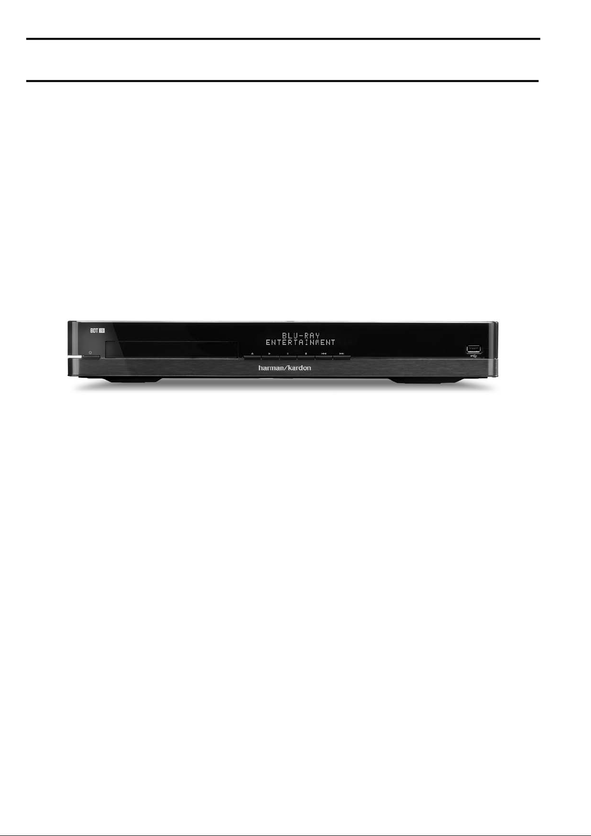
harman/kardon Service Manual
BDP 20/230
BDP 2/120
Blu-ra y p laye r
FRONT PANEL CONTROLS 3
REAR-PANEL CONNECTIONS 4
REMOTE CONTROL FUNCTIONS 5
TROUBLESHOOTING 6
SPECIFICATIONS 7
SOFTWARE UPGRADE INSTRUCTIONS 8
EXPLODED VIEW 14
BDT 2 PARTS LIST 15
BDT 20 PARTS LIST 16
PCB DRAWINGS 17
WIRING DIAGRAM 22
SCHEMATIC DIAGRAMS 23- 37
IMPORTANT INFORMATION ABOUT PAIRING A NEW LOADER WITH THE MAIN BOARD
ON PAGE 38-39.
Released EU2011 Harman Consumer Group, Inc. Rev 1, 03/2012
8500 Balboa Boulevard
Northridge, California 91329
Page 2
BDT 2/BDT 20
harman/kardon
BDT 2 / BDT 20 Service Manual
Page 2 of 37
BDT 2/BDT 20 Features
BDT 2/BDT 20 Features
Connectivity
One HDMI ver. 1.3a with 30/36-bit Deep Color connection •
One coaxial digital-audio output •
One USB 2.0 port that plays video, audio and photo content from USB devices •
Connects to your LAN (local area network) for BD-Live interactivity via the Internet •
Ease of Use
On-screen menu system •
Dot-matrix front-panel information display •
Full-function remote control •
Disc Player Features
Region coding: Blu-ray Disc Region A/DVD Region 1 (BDT 2 models); •
Blu-ray Disc Region B/DVD Region 2 (BDT 20 models)
Plays five-inch (12cm) and 3-inch (8cm) discs •
Video formats supported: BD-Video (single-layer or double-layer), DVD-Video, •
DVD+R/+RW, DVD-R/-RW, CDDA (CD digital audio), CD-R/RW
Audio formats supported: Dolby •
Digital, DTS-HD™ High Resolution Audio, DTS-HD Master Audio,™ PCM, WMA
(DRM-free version only): WMA9, CBR @192kbps, VBR @ 355kbps, MP3: 32kbps –
320kbps bitrates, including variable bitrate encoding
Supports JPEG still-image format •
Supports BD-Live interactivity •
Video upscaling to 720p and 1080p •
Progressive-scan video output •
JPEG resolution supported: five megapixels, 5MB file size •
JPEG still-image rotation in 90-degree increments •
Thumbnail JPEG still-image menu •
Fast play rates: 2x, 4x, 8x, 16x, 32x •
Slow play rates: 1/2x, 1/4x, 1/8x, 1/16x •
Random play (CDs only) •
Repeat play •
Parental-control system with user-programmable password •
Disc recognition for up to 10 discs •
Aspect-ratio adjustment •
®
Digital, Dolby Digital Plus, Dolby TrueHD, DTS
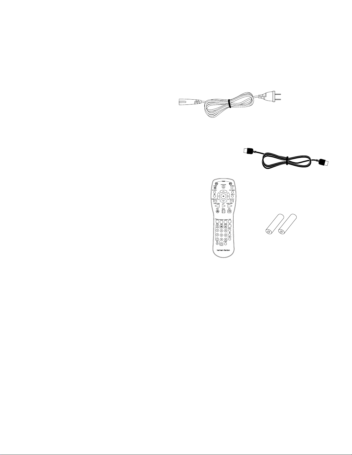
Supplied Accessories
If any of these items are missing, please contact Harman Kardon Customer Service via
www.harmankardon.com.
Power cord
(Note: The power cord included will
vary depending on where the unit
is sold.)
®
Remote control
HDMI cable
Two AA batteries
6
Page 3
BDT 2/BDT 20
harman/kardon
BDT 2 / BDT 20 Service Manual
Page 3 of 37
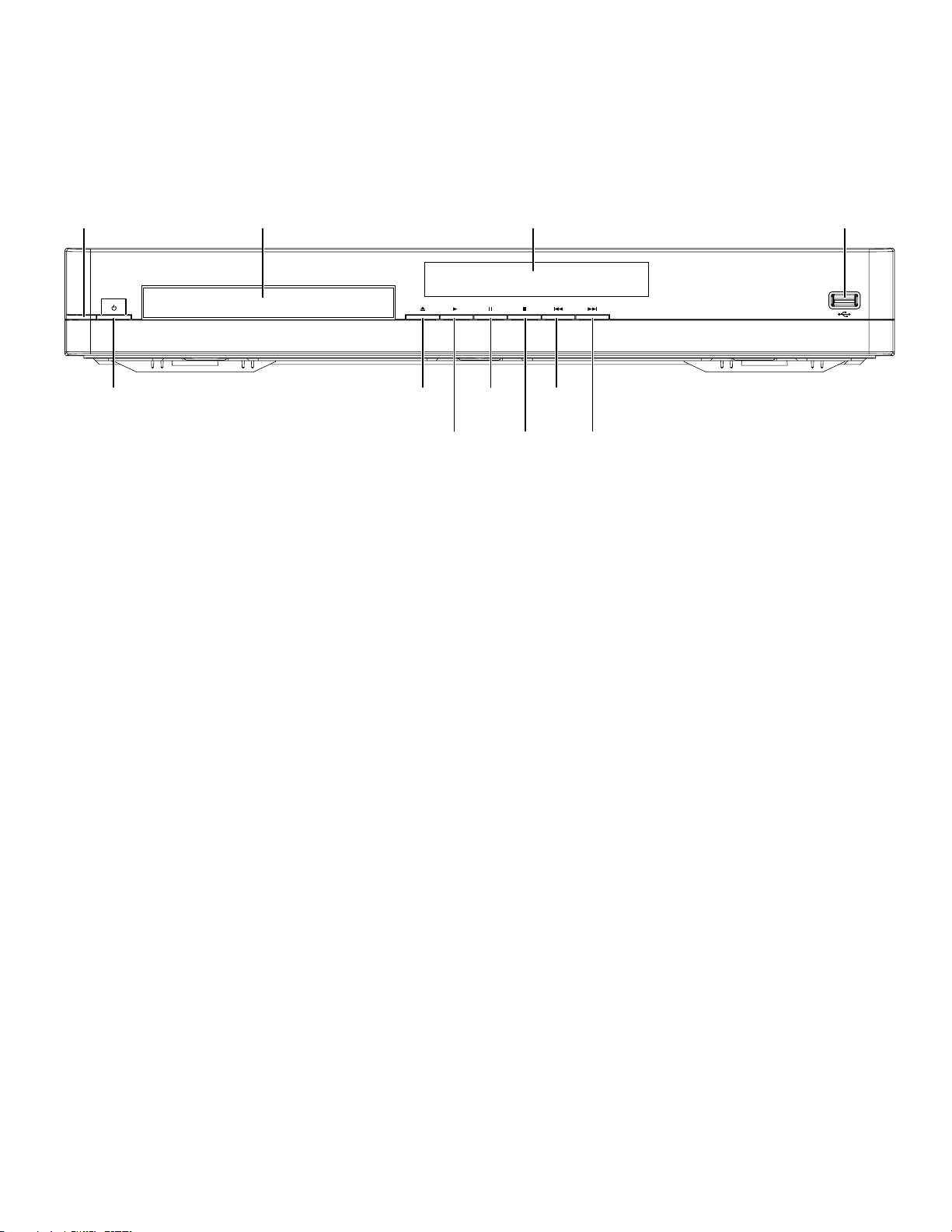
Front-Panel Controls
Front-Panel Controls
Power
Indicator
Power
Button
Power Indicator:
switch is set to “On,” the LED turns amber to indicate that the player is in Standby mode.
When you turn the BDT 2/BDT 20 on (by the Power button or the remote control), the
LED turns white.
Power Button
modes.
Disc Drawer:
5-inch (12cm) and 3-inch (8cm) discs.
Open/Close Button:
this button, make sure that no objects are blocking the disc drawer.
Play Button:
drawer. Pressing this button when viewing photos begins a slide show with all photos in
the current folder.
Pause Button:
while a Blu-ray Disc program or DVD program is playing will freeze-frame on the current
video frame. Pressing the button while the disc is paused will resume play. Pressing this
button while viewing photos freezes the current photo on the screen.
Stop Button:
button will resume playback from the point where it stopped.) Press the Stop button
twice to stop playback fully.
When the BDT 2/BDT 20 is plugged into AC power and its Main Power
: This button toggles the BDT 2/BDT 20 between the On and Standby
Insert a compatible disc into the drawer. The BDT 2/BDT 20 will accept
Press this button to open and close the disc drawer. Before pressing
Press this button to play a disc that has been loaded into the player’s disc
Press this button to pause a disc that is playing. Pressing the button
Press this button to stop playback. (With some discs, pressing the Play
Disc
Drawer
Open/Close
Button
Play
Button
Information
Display
Pause
Button
Previous/
Step
Button
Stop
Button
Information Display:
and to provide information about the BDT player’s status as described throughout this
manual.
Previous/Step Button:
or chapter being played – or, when viewing photos, to the previous photo. Press the
button twice to skip to the beginning of the previous chapter or track. Press the button
repeatedly to skip back through the previous chapters or tracks. When video content is
playing, press the Pause button, after which each press of the Previous/Step button will
step the video back by one frame.
Next/Step Button:
chapter – or, when viewing photos, to the next photo. Press the button repeatedly to skip
ahead through the subsequent chapters or tracks. When video content is playing, press
the Pause button, after which each press of the Next/Step button will step the video
forward by one frame.
USB Port:
cable to this port.
IMPORTANT:
may damage both the BDT 2/BDT 20 and your device.
Orient the device’s plug so it fits all the way into the BDT 2/BDT 20’s USB connector.
You may insert or remove the device at any time – there is no installation or ejection
procedure.
Next/Step
Button
Various messages appear on this display in response to commands
Press this button once to skip to the beginning of the track
Press this button once to skip to the beginning of the next track or
Gently insert a USB flash drive or an HDD disk drive with a USB Standard-A
Do not connect a PC or other USB host/controller to this port, or you
USB
Port
7
Page 4
BDT 2/BDT 20
ON OFF
harman/kardon
BDT 2 / BDT 20 Service Manual
Page 4 of 37
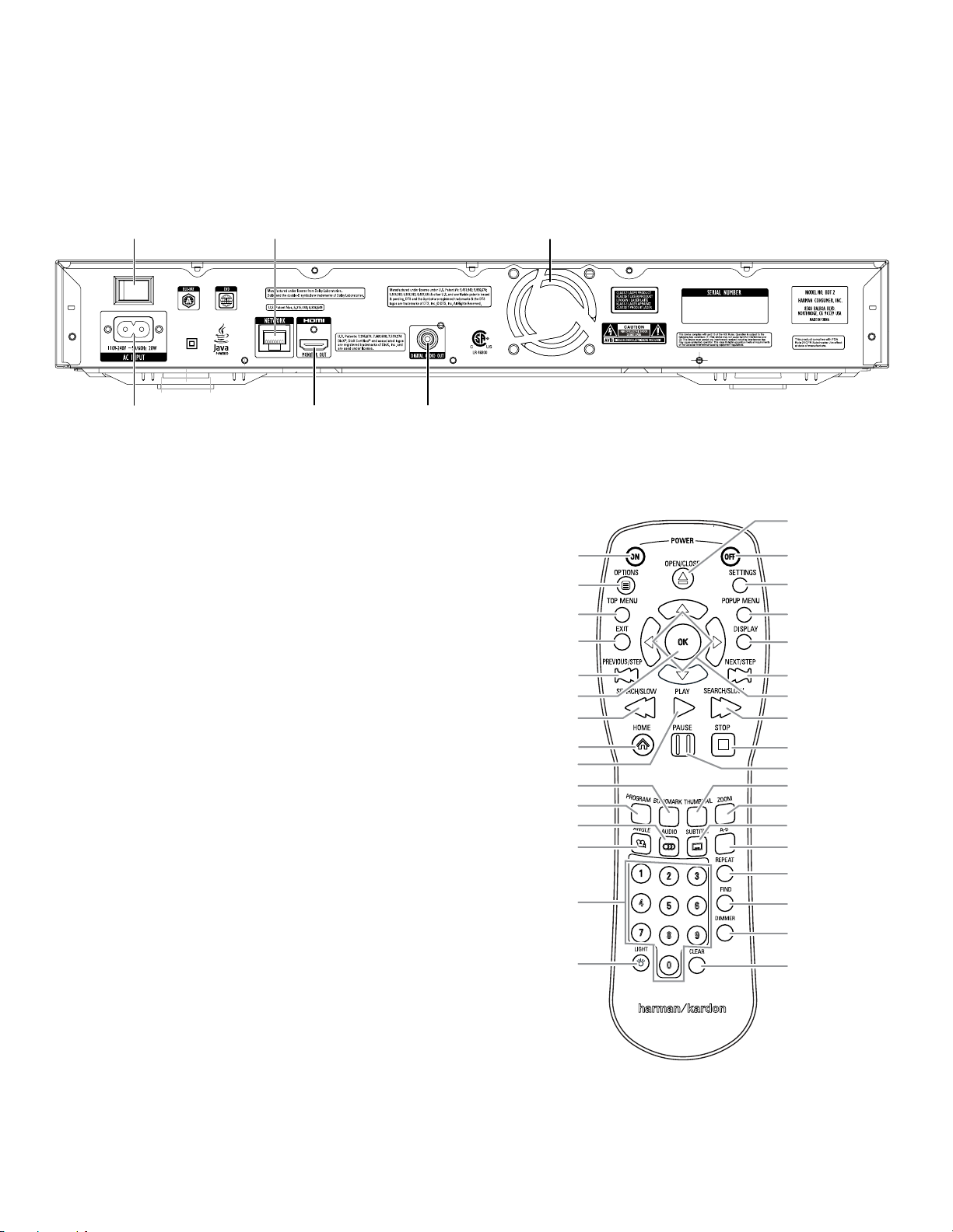
Rear-Panel Connections
Rear-Panel Connections/Remote Control Functions
Main Power
Switch
Power-Cord
Connector
NOTE: See Connecting the Player, on page 10, for detailed information
about making connections.
Main Power Switch: This mechanical switch turns the BDT 2/BDT 20’s power
supply on or off. After you have made and verified all connections (see Connecting
the Player, on page 10), set this switch to the “On” position. If you will not be using
the player for an extended period of time, you can set this switch to the “Off” position
to save energy.
Power-Cord Connector: After you have made and verified all other connections,
plug the supplied AC power cord into this input and into an unswitched AC outlet.
Network Connector: To be able to use the BD-Live feature, connect this port to
your local area network (LAN) using a Cat. 5/Cat. 5e/RJ45 network cable. See
BD-Live Interactivity, on page 15, for more information.
HDMI Output (HDMI ver. 1.3a): Connect the BDT player’s HDMI output to the HDMI
input on your TV, audio/video receiver or surround-sound processor. The HDMI cable
transmits both video and audio, so if you’re connecting it directly to the TV and are
connecting the BDT 2/BDT 20’s coaxial digital audio output to a home theater audio
system, we recommend that you disable the BDT 2/BDT 20’s HDMI Audio Out to take
full advantage of the home theater audio system’s superior audio performance. See
Audio Settings: Audio Output, on page 13, for more information.
IMPORTANT: Your BDT 2/BDT 20 is in compliance with HDCP (High-Definition Copy
Protection). Your TV must also be HDCP-compliant to be used with the player’s HDMI
output. For the best results, we do not recommend HDMI connections in excess
of ten feet without a repeater. If your TV has a DVI input, you may use an optional
HDMI-to-DVI cable or adapter for the video connection to the TV. (The DVI connection
is video-only.)
Coaxial Digital Audio Output: Connect this output to the coaxial digital audio input
of your audio/video receiver or surround-sound decoder.
Fan Vents: The BDT 2/BDT 20 has a built-in fan to provide cooling air. To insure
proper operation, make sure that these vents are not blocked.
Network
Connector
HDMI
Output
Coaxial Digital Audio
Output
Fan
Vents
Remote Control Functions
Power On Button
Options Button
Top Menu Button
Exit Button
Prev/Step Button
OK Button
Search/Slow
Reverse Button
Home Button
Play Button
Bookmark Button
Program Button
Audio Button
Angle Button
Numeric Buttons
Open/Close Button
Power Off Button
Settings Button
Popup Menu Button
Display Button
Next/Step Button
Cursor Button
Search/Slow
Forward Button
Stop Button
Pause Button
Thumbnail Button
Zoom Button
Subtitle Button
A-B Button
Repeat Button
Find Button
Dimmer Button
8
Backlight Button
Clear Button
Page 5

BDT 2/BDT 20
harman/kardon
BDT 2 / BDT 20 Service Manual
Page 5 of 37
Remote Control Functions
Open/Close Button:
this button, make sure that no objects are blocking the disc drawer.
Power On Button:
to turn it on.
Power Off Button:
Standby mode.
Options Button:
active at the time you press the button.
Settings Button:
Menus
, on page 12, for more information.
Top Menu Button:
recording or DVD that is playing. NOTE: This feature is disc-dependent. Not all DVDs have
top menus. If the DVD has no top menu, pressing the Top Menu button may display the
disc menu, depending on how the disc’s menu system was authored.
Popup Menu Button:
displays its disc menu. NOTE: This feature is disc-dependent. Not all discs have pop-up
menus. If a DVD has no pop-up menu, pressing the Popup Menu button may display the
disc menu, depending on how the disc’s menu system was authored.
Exit Button:
Display Button:
the disc or program that is currently playing.
Previous/Step Button:
track – or when viewing photos, to the previous photo. Press the button twice to skip
to the beginning of the previous track. Press the button repeatedly to step through the
previous chapters or tracks. When video content is playing, press the Pause button, after
which each press of the Previous/Step button will reverse the video by one frame.
Next/Step Button:
when viewing photos, to the next photo. Press the button repeatedly to step through the
previous chapters or tracks. When video content is playing, press the Pause button first;
each subsequent press of the Next/Step button advances the video one frame.
OK Button:
Cursor Buttons:
menu.
Search/Slow Reverse Button:
track. For Blu-ray Disc programs and DVD programs, each press cycles through 2x, 4x,
8x, 16x and 32x reverse speed. Pressing the button while a Blu-ray Disc recording or DVD
is paused will reverse through the chapter in slow motion. Each press cycles through 1/2,
1/4, 1/8 and 1/16 normal speed.
Search/Slow Forward Button:
For Blu-ray Disc recordings and DVDs, each press cycles through 2x, 4x, 8x, 16x and 32x
normal speed. Pressing the button while a Blu-ray Disc recording or DVD is paused will
play through the chapter in slow motion. Each press cycles through 1/2, 1/4, 1/8 and
1/16 normal speed.
Home Button:
whatever screen is active when the button is pressed.
Stop Button:
playback from the point where it stopped.) Press the Stop button twice to stop playback
fully. NOTE: Some settings and functions will only be available when the player is fully
stopped.
Play Button:
drawer or a music file that has been highlighted on the on-screen menu. Pressing this
button when viewing photos begins a slide show of the photos.
Pause Button:
the button while a Blu-ray Disc program or DVD program is playing will freeze-frame on
the current video frame. Pressing the button while the disc is paused will resume play.
Pressing this button while viewing photos freezes the current photo on the screen.
Press this button to open and close the disc drawer. Before pressing
Press this button when the BDT 2/BDT 20 is in the Standby mode
Press this button when the BDT 2/BDT 20 is on to place it in the
Press this button to display any available options for the item that is
Press this button to display the player’s Settings menu. See
Press this button to display the top menu of the Blu-ray Disc
Pressing this button while playing a Blu-ray Disc recording or DVD
Press this button to return to the previous menu or menu level.
Press this button to activate a bar display containing information about
Press this button once to skip to the beginning of the current
Press this button once to skip to the beginning of the next track or
Press this button to select a highlighted item on the on-screen menu.
Press these buttons to navigate through items on the on-screen
Press this button to reverse through the current disc
Press this button to fast-forward through a disc track.
Press this button to return the on-screen display to the Home screen from
Press this button to stop playback. (Pressing the Play button will resume
Press this button to play a disc that has been loaded into the player’s disc
Press this button to pause a disc or music file that is playing. Pressing
Settings
Bookmark (green) Button:
Bookmark Function, on page 15, for more information.
Thumbnail (yellow) Button:
display thumbnail images of all photos in the active directory.
Program (red) Button:
disc that is playing. See Programmed Play, on page 15, for more information.
Zoom (blue) Button:
slide. Use the Navigation buttons to zoom in on different sections of the image. NOTE:
This function is disc-dependent. Not all discs allow this function.
Red, green, yellow and blue buttons:
recording, these buttons can activate features and menus that may vary from disc to
disc. Refer to the menu instructions for each particular disc for more information. NOTE:
These Blu-ray Disc functions may override the Bookmark, Thumbnail, Program and Zoom
functions.
Audio Button:
available for a disc. NOTE: This feature is disc-dependent. Not all discs feature multiple
audio tracks and allow you to change audio tracks.
Subtitle Button:
are available for the current disc. NOTE: This feature is disc-dependent. Not all discs
feature multiple subtitle options.
Angle Button:
for the current disc. NOTE: This feature is disc-dependent. Not all discs feature multiple
camera angles and allow you to change camera angles.
A-B Button:
“A” repeat point; the second press sets the “B” repeat point and begins repeating the
section of the program between the two points. Pressing the A-B button while the A-B
repeat mode is active cancels the A-B repeat mode.
Repeat Button:
press this button to cycle through the following repeat modes: Chapter, Title, All, Off.
When the BDT 2/BDT 20 is playing a CD, this button cycles through the following repeat
modes: Track, All, Off.
Numeric Buttons:
Find Button:
which allows you to jump to a specific location on the disc. You can find a location by
title, chapter or elapsed time.
Dimmer Button:
the player’s front-panel display: 100%, 50%, 25%, Auto/Off. When the brightness is set
to Off, the display will temporarily return to full brightness whenever you press any button
on the remote.
Backlight Button:
will remain on for a few seconds and then will turn off to conserve battery power.
Clear Button:
buttons.
Press this button to toggle through the different audio tracks that are
Press this button to toggle through the different subtitle options that
Press this button to toggle through the multiple camera-angle options
Press this button to activate the A-B repeat mode. The first press sets the
When the BDT 2/BDT 20 is playing a Blu-ray Disc recording or DVD,
Press this button during disc playback to activate the search function,
Press this button to toggle through the different brightness levels for
Press this button to clear an incorrect entry made using the Numeric
Press this button to activate the Bookmark function. See
Press this button while playing a photo slide show to
Press this button to create a programmed playback list for the
Press this button to zoom in on or recede from a video image or
When the BDT 2/BDT 20 is playing a Blu-ray Disc
Press these buttons to enter numbers for various items.
Press this button to activate the remote’s backlight. The backlight
9
Page 6

BDT 2/BDT 20
harman/kardon
BDT 2 / BDT 20 Service Manual
Page 6 of 37
Troubleshooting
Troubleshooting
If your BDT 2/BDT 20 isn’t performing the way you think it should, check to see if the problem is covered in this section before calling your dealer or contacting Harman Kardon.
Problem Solution
The player won’t power up (the Power indicator is not lit ): Check that the player’s AC power cord is properly plugged into the player’s power- •
The disc does not play: Check that the disc is inserted correctly (label side up). •
No picture: Check the connection between the player and the TV. •
No sound: Check that the HDMI and/or coaxial digital connections are properly made. •
The picture appears in the wrong aspect ratio: Change the Aspect Ratio setting in the Display Settings menu to match the TV. •
There is noise or other interference in the picture while playing a Blu-ray Disc
recording or DVD:
Cannot access media on a connected USB device: Check that the device is formatted in the FAT32 file system. Other file systems are •
The player does not respond to remote-control commands: Replace both remote-control batteries with fresh ones, and make sure that they are •
cord connection.
Check that the player’s AC power cord is plugged into a working AC outlet and that •
the AC outlet is not controlled by a switch.
Make sure that the Master Power switch (on the player’s rear panel) is in the “On” •
position.
Check that the disc is the correct type: BD-Video (single-layer or double-layer), •
DVD-Video, DVD+R/+RW, DVD-R/-RW, CDDA (CD digital audio), CD-R/RW. Other
disc types will not play.
Check that the TV is turned on and that it is set to the correct input source. •
Confirm that all of the choices made in the Display Settings menu are correct for •
your TV.
Check that the TV is HDCP-compliant. The player cannot be used with a TV that is •
not HDCP-compliant.
If you’re using the coaxial digital connection, check that the digital audio settings on •
the connected device have been properly set.
If you’re using only the HDMI connection, check that the HDMI audio settings on the •
connected device have been properly set.
If you’re using only the HDMI connection, check that the BDT 2/BDT 20’s HDMI •
Audio Output is set to “On.”
Check that the disc surface is clean and not scratched. •
not compatible with the BDT 2/BDT 20.
installed correctly.
Hold the remote control closer to the player. •
Check that the player’s remote sensor is in the remote control’s line of sight. •
Make sure that the protective shipping film has been removed from the player’s •
front panel.
The Ø symbol appears on the screen when you press a remote-control button: The selected function is not permitted at the time you press the button. •
The player does not respond to commands, or it behaves in an erratic way: Unplug the player’s power cord from the AC outlet, wait 30 seconds, and plug it •
You can find ad ditional troublesho oting infor mation in th e FAQs link on th e Suppor t page at ww w.harmanka rdon.com.
back in.
19
Page 7

BDT 2/BDT 20
harman/kardon
BDT 2 / BDT 20 Service Manual
Page 7 of 37
Specifications
Specifications
Supported disc formats: 5-inch (12cm) or 3-inch (8cm) BD-Video (single-layer or double-layer), DVD-Video,
Region code (BD/DVD): A/1 (BDT 2); B/2 (BDT 20)
Audio formats: Dolby Digital, Dolby Digital Plus, Dolby TrueHD, DTS Digital, DTS-HD High Resolution
Still-image format: JPEG
Video signal system: NTSC (BDT 2); PAL (BDT 20)
HDMI version: 1.3a with 30/36-bit Deep Color
Power requirement: AC 100 – 240V, 50/60Hz
Power consumption: 25W maximum, <1W standby
Dimensions (H x W x D): 2-5/8" x 17-5/16" x 13-7/8" (66mm x 440mm x 352mm)
Weight: 8.2 lb (3.7kg)
Depth includes Volume button and loudspeaker terminals.
DVD+R/+RW, DVD-R/-RW, CDDA (CD digital audio), CD-R/RW discs
Audio, DTS-HD Master Audio, PCM, WMA (DRM-free version only): WMA9, CBR
@192kbps, VBR @ 355kbps, MP3: 32kbps – 320kbps bitrates, including variable
bitrate encoding
Page 8

4-1
harman/kardon
BDT 2 / BDT 20 Service Manual
Page 8 of 37
Software upgrade
Preparation to upgrade software
1.Power on the set and press “settings” button on the remote.
2.Press left cursor to select "Information" .check the Software Version.
3. According the software version to check the correct software in UPG folder.
For example:if the software version is display “BDT20 XX.XX.XX”,the correct
software is “BDT20_BD.bin”,otherwise the software is “BDT2_BD.bin”.
4.Start the CD Burning software and cr eate a new CD project (Data Disc),copy
the UPG folder to the root directory of data disc.
5.Burn the data onto a blank CDR
Procedure for software upgrade:
A) Upgrade software via CDR:
1.Power on the set and insert the prepared Upgrade CDR.
2.The set will starts reading disc .
3.When the set recognize the disc,press Setting-->System-->System
Upgrade-->Disc, follow the instructions on the screen.
4.About 3 minute later,the set will automatically turn off when upgrading
completed.
B) Upgrade software via USB Flash Drive:
1.Decompress the packed file, copy the UPG folder to the root directory of a
USB memory device.
2.Insert the USB, the player will recognize the USB device automatically.
3.Press Setting-->System-->System Upgrade-->Disc, follow the instructions on
the screen.
4.About 3 minute later,the set will automatically turn off when upgrading
completed.
Read out the software versions to confirm upgrading
1.Power on the set and press “settings” button on the remote.
2.Press left cursor on remote control to select "Information" .The software
version and other informations will be displayed on the TV screen as follows:
Software Version: BDTX XX.XX.XX
Mac Address:XX-XX-XX-XX-XX-XX
Caution: The set must not be pow er off during upgrading, Otherwise the
Main board will be damaged entirely.
Page 9
5-1
harman/kardon
BDT 2 / BDT 20 Service Manual
Page 9 of 37
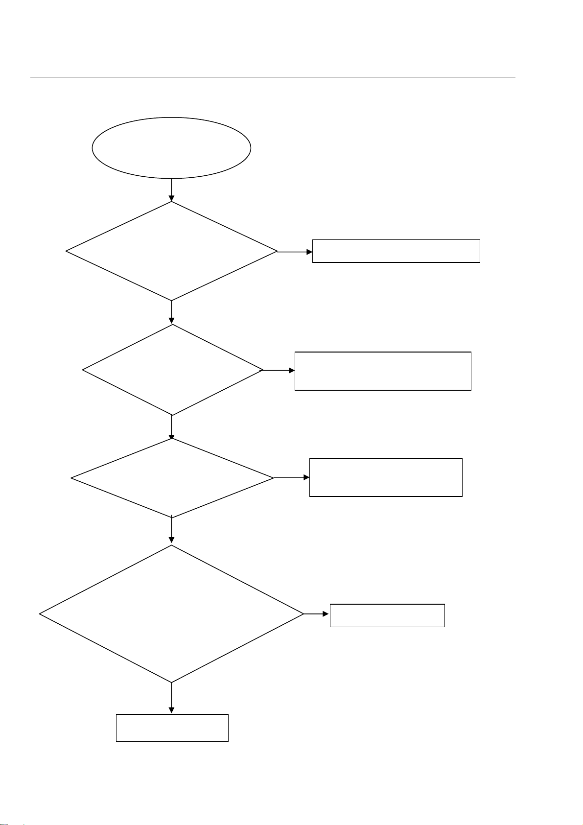
Trouble shooting chart
No display on VFD, and buttons do not work
No disp lay on VF D, and
buttons do not work
Yes
Check ever y suppl y
voltage on main board is
normal
No
Refer to Power supply board part
Yes
Check38V,5V,+12V
voltage on th e po wer
and front board
No
Fix the c onnection XS603 on front
board and ZD602
Yes
Check th e front bo ard
signal VDIN,VCLK,
VSTB,
No
Check the U721’s pin 61,60,59singal
Yes
1.Check whether bad so lder exist s
on U721 and pins of VFD,
2.Check w hether the circuit
connected to K7, K2, K3, K4, K5,
K6 is broken.
No
Correct connection
Yes
Replace U721
Page 10
harman/kardon
BDT 2 / BDT 20 Service Manual
Page 10 of 37
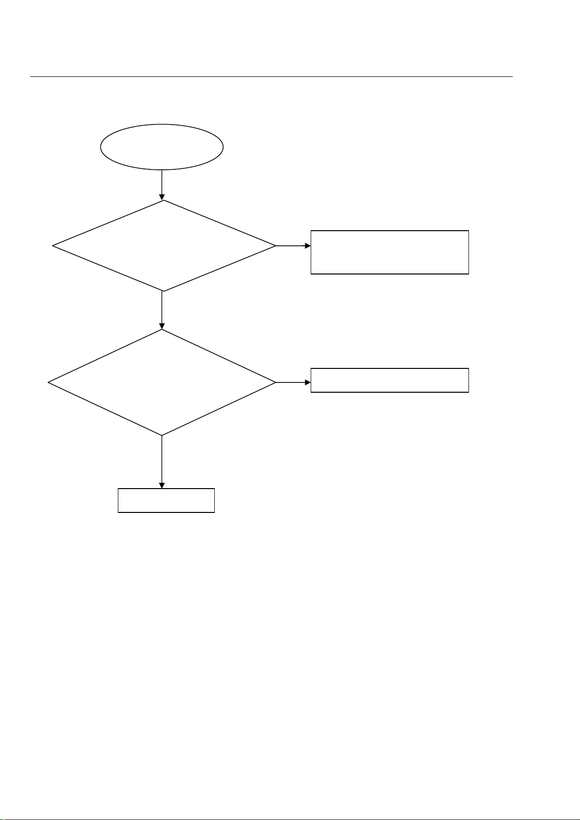
Remote control does not work
Remote c ontrol
does not work
Go
Check whether the remote
controller’s batter y is
exhausted or not.
NO
Check the IR1 power
supply+3.3V_STBIR
Yes
Replace IR1
Yes
5-2
yes
No
Trouble shooting chart
Replace th e batter y for remote
controller
Check the +3.3 V net no front board
Page 11
5-3
harman/kardon
BDT 2 / BDT 20 Service Manual
Page 11 of 37
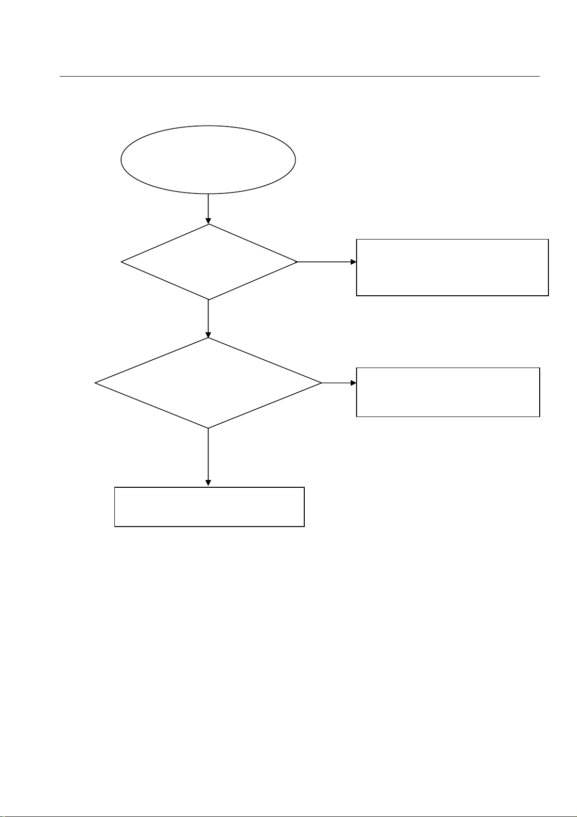
Can’t read disc or can’t open the disk door
Can’t rea d disc or can’t
open the disk door
GO
Check w hether the
DVD loa der ru nning is
normal
Yes
Check SA TA cable from
main bo ard conn ection to
the loader is normal
Yes
Replace the loader
Trouble shooting chart
NO
NO
Check the c onnection of the 4PIN cabl e h e
Power Board.
Fix the connection the And SATA cable from
main board
Page 12
5-4
harman/kardon
BDT 2 / BDT 20 Service Manual
Page 12 of 37
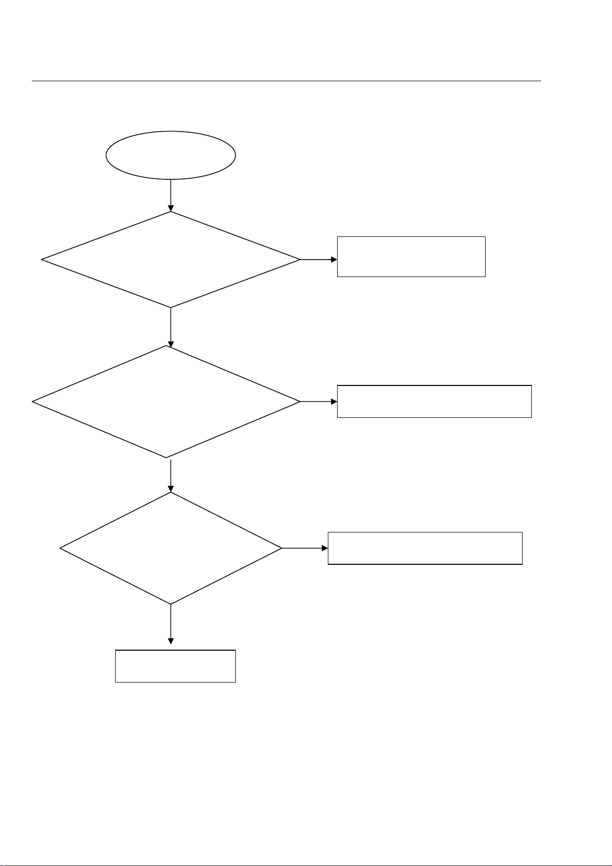
No VFD display
No VFD display
Go
Check whether the volt age
5V,12V on th e front bo ard is
normal work or not.
Yes
Check whether the volt age
between VF D F+ &VFD F- is
DC 4V+/-0.4
Yes
No
No
Fix the conn ection po wer board
CN502 front board XS603
Check DC12V to
Trouble shooting chart
AC 4V switch circuit
Check w hether the
voltage 38 V is normal
Replace U
602
No
Check the ZD602 on the front board
Page 13

5-5
harman/kardon
BDT 2 / BDT 20 Service Manual
Page 13 of 37
Fan don’t work
Fan don’t work
Go
Check on P ower bo ard
whether CN5 03.1 is
+12V
No
Check Q511.8 on Power board
Yes
Check th e cabl e
connection fan to Po wer
board CN503
No
Replace the cable
Yes
Trouble shooting chart
Replace Fan
Page 14

8-1
harman/kardon
BDT 2 / BDT 20 Service Manual
Page 14 of 37
ASSY1
Exploded view for BDT2 and BDT20 :
8-1
RemarkÿThis is general mechanical exploded view for BDT2 and BDT20 .Please refer to the model set for the detailed information.
ASSY1 includes components:1,2,3,4,5,6,7,8,9,10,11,13,39,40,41,42,43
Page 15

BDT2 SERVICE PARTS
harman/kardon
BDT 2 / BDT 20 Service Manual
Page 15 of 37
Location No. TCL P/N. Description Q'ty
27 08-0BDT20-MAN
38 08-0BDT20-VFD
29 08-0BDP20-PW1
12 08-BDP100-PSW
08-00BDP1-SW0
16 08-BL1419-LD2
OPU 05-BD10YL-001
ASSY1 08-BDT2F1-XX0
08-00BDP1-XXO
18 67-BDP1T1-0E0B1
19 67-BDT2B1-0E0B1
20 43-FS512S-216
24 51-BC0150-0LSA9-M
32 58-983770-0HH
33 56-BDP1E1-0HA
34 54-981610-000
HDMI 46-HDI010-19G01
23 46-35063W-03X-M
67-BDT2R1-0E0B1
USB 47-USB013-XX1
8-2
ASSY-MAIN BOARD
ASSY-FRONT CONTROL BOARD
ASSY-POWER BOARD
ASSY-PS BD
ASSY-SW BD
ASSY-LOADER BD
YINGlANG TRAVERSE BD412V OPU
ASSY-FRONT PANEL
ASSY-DECORATIVE ALUMINIUM-BAR
TOP COVER
BACK PANEL
DC FAN 5012F 320mm
USA POWER CORD 1.5m
PET PLATE
FOOT
RUBBER PAD
HDMI CABLE 1m
POWER SOCKET
BOTTOM PLATE
USB SOCKET BLACK
1
1
1
1
1
1
1
1
1
1
1
1
1
2
4
4
1
1
1
1
REMARK:
ASSY1 includes components:1,2,3,4,5,6,7,8,9,10,11,13,39,40,41,42,43
SAFETY PRECAUTION
The parts identified by mark are critical for safety. Replace only with part number
specified. The mounting position of replacement is to be identical with originals.
The substitute replacement parts which do not have the same safety characteristics as
specified in the parts list may create shock, fire or other hazards.
Page 16

BDT20 SERVICE PARTS
harman/kardon
BDT 2 / BDT 20 Service Manual
Page 16 of 37
Location No. TCL P/N. Description Q'ty
27 08-0BDT20-MAN
38 08-0BDT20-VFD
29 08-0BDP20-PW2
12 08-BDP100-PSW
08-00BDP1-SW0
16
OPU 05-BD10YL-001
ASSY1 08-BDT2F2-XX0
18 67-BDP1T1-0E0B1
19 67-BDT2B1-0E0B2
20 43-FS512S-216
24 51-DC0150-0CRA3-M
32 58-983770-0HH
33 56-BDP1E1-0HA
34 54-981610-000
HDMI 46-HDI010-19G01
23 46-35063W-03X-M
USB 47-USB013-XX1
08-BL1419-LD2
08-00BDP1-XXO
67-BDT2R1-0E0B1
8-3
ASSY-MAIN BOARD
ASSY-FRONT CONTROL BOARD
ASSY-POWER BOARD
ASSY-PS BD
ASSY-SW BD
ASSY-LOADER BD
YINGlANG TRAVERSE BD412V OPU
ASSY-FRONT PANEL
ASSY-DECORATIVE ALUMINIUM-BAR
TOP COVER
BACK PANEL
BOTTOM PLATE
DC FAN 5012F 320mm
EUROPEAN POWER CORD 1.5m
PET PLATE
FOOT
RUBBER PAD
HDMI CABLE 1m
POWER SOCKET
USB SOCKET BLACK
1
1
1
1
1
1
1
1
1
1
1
1
1
1
2
4
4
1
1
1
REMARK:
ASSY1 includes components:1,2,3,4,5,6,7,8,9,10,11,13,39,40,41,42,43
SAFETY PRECAUTION
The parts identified by mark are critical for safety. Replace only with part number
specified. The mounting position of replacement is to be identical with originals.
The substitute replacement parts which do not have the same safety characteristics as
specified in the parts list may create shock, fire or other hazards.
Page 17
7-16
harman/kardon
BDT 2 / BDT 20 Service Manual
Page 17 of 37
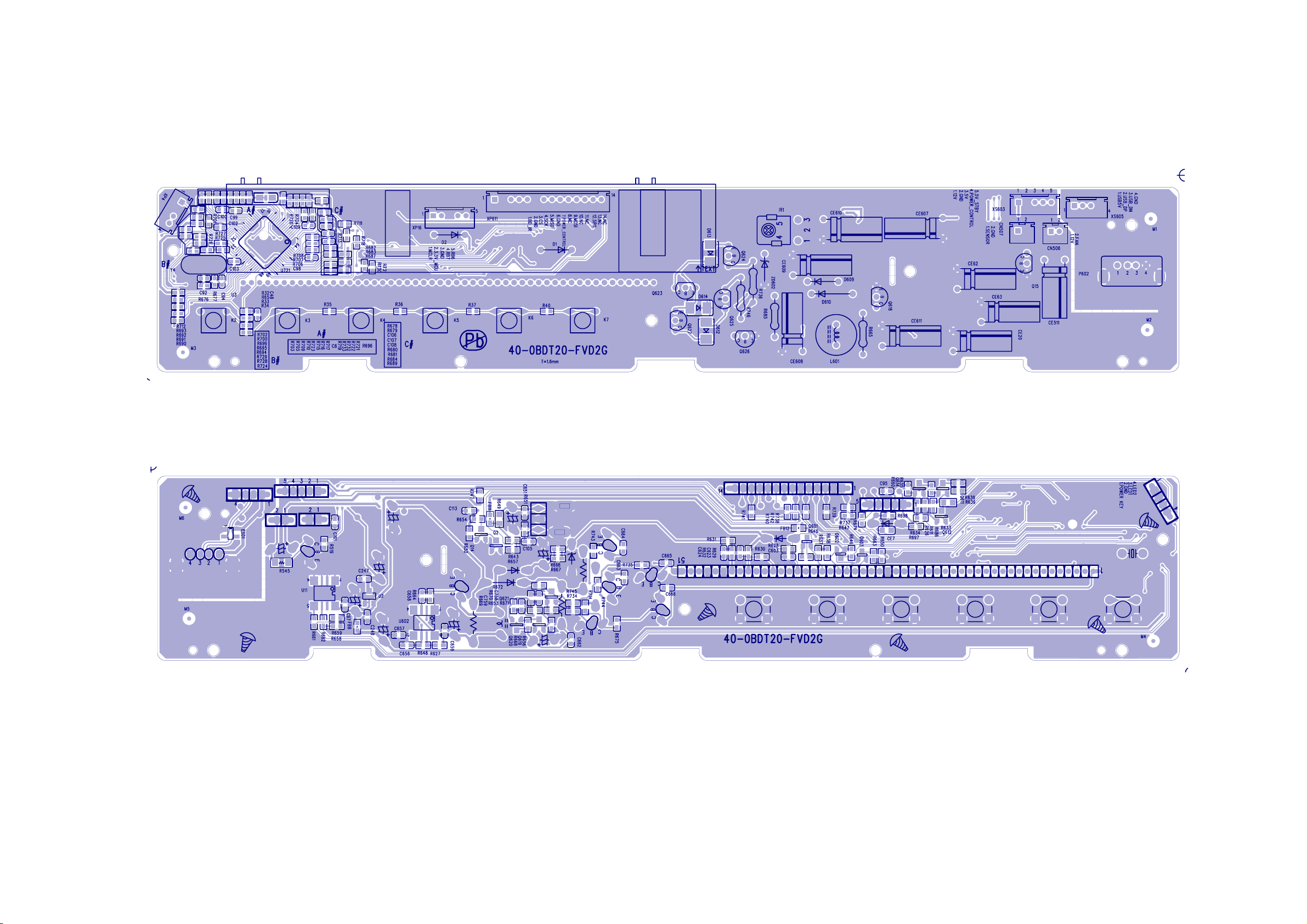
Front Control Board Print-layout (top and bottom sides):
7-16
Page 18

7-17
harman/kardon
BDT 2 / BDT 20 Service Manual
Page 18 of 37
Power Supply Print-layout (top side):
7-17
Page 19

7-18
harman/kardon
BDT 2 / BDT 20 Service Manual
Page 19 of 37
Power Supply Print-layout (bottom side):
7-18
Page 20

7-19
harman/kardon
BDT 2 / BDT 20 Service Manual
Page 20 of 37
Main Board Print-layout (top side):
7-19
Page 21

7-20
harman/kardon
BDT 2 / BDT 20 Service Manual
Page 21 of 37
Main Board Print-layout (bottom side):
7-20
Page 22

6-1
harman/kardon
BDT 2 / BDT 20 Service Manual
Page 22 of 37
6-1
A
1 1
DISC
MAN BOARD
B
COAX OUT
BDT2
& BDT20 WIRING DIAGRAM
HDMI Port
0524P
0524P
C
RJ-45
D
E
FAN
SMSC8710
3.3V
110-240V/50~60Hz
3.3V
2 2
TPC1391G4
45PIN
NAND
Flash
3.3V
3.3V
5V
4PIN
Motor Driver
3 3
POWER/STANBY
BOARD
K1
IR
4 4
K2
K3 K4 K5 K6
VFD BOARD
VFD
8PIN
K7
R2A30209P
5V
12V
14PIN
IR
VCLK
VSTB
14PIN
MCU
VDATA
LCDRD
MOSI
PWR_CTRL#
4PIN
DP
5V
USB
12V
5V
PCON
DN
5V_STBY
GND
MT8530/BGA
DDR
DDR
1.1V
1.2V
1.8V
5V
12V
PCON
5V_STBY
12V
5V
DDR
DDR
1.8V
1.8V
1.8V
TPS65230
8PIN
-12V
+12V
5V
5V
FAN+
FAN-
ON/OFF
2PIN
POWER BOARD
8PIN
5PIN
A
B
C
D
E
Page 23

7-1
harman/kardon
BDT 2 / BDT 20 Service Manual
Page 23 of 37
7-1
A
B
C
D
E
Front Control Board Circuit Diagram:VFD
5V_STBY
Q612
Q612
MMBT8550C
R634 0R634 0
POWER_control A
POWER_control A
1 1
R626
R626
Q611
MMBT8550C
MMBT8550C
R611
R611
4.7K
R6351KR635
1K
10K
10K
Q614
Q614
R660
R660
MMBT8050C
MMBT8050C
47K
47K
4.7K
R6391KR639
1K
MMBT8550C
R686 220R686 220
Q611
2 2
POWER_control
XS603
XS603
5
5
4
4
3
3
2
2
1
1
5PIN/2.0mm
5PIN/2.0mm
TO POWER BOARD
3 3
5V_STBY
POWER_control
VT5V 5V
12V
TP75TP75
POWER_control
TP72TP72
TP73TP73
TP76TP76
TP74TP74
CE608
CE608
47uF/16V
47uF/16V
C662
C662
+
+
0.1uF
0.1uF
R669 10KR669 10K
C759
C759
1200pF
1200pF
R668
R668
10K
10K
Q620
Q620
MMBT8050C
MMBT8050C
Q619
Q619
MMBT8050C
MMBT8050C
R656 1kR656 1k
R633 560R633 560
R636
R636
12V
47uF/16V
47uF/16V
R653
R653
470
470
330
330
CE607
CE607
LED1
LED2
12V
+
+
R685 470R685 470
R670 4.7KR670 4.7K
C758
C758
0.1uF/50V
0.1uF/50V
MMBT8050C
MMBT8050C
Q621
Q621
R671
R671
10K
10K
R66556R665
D610
D610
1N4007
1N4007
R6721kR672
1k
LED1
LED2
VSTB_1
56
U602
U602
SA555
SA555
R648 12KR648 12K
V12V
7
8
DA
VCC
GND1TG2OUT3RESET
10K
10K
220
220
6
C656
C656
1000pF
1000pF
5
TS
CV
C657
C657
1000pF
1000pF
100pF
100pF
C658
V12V
R714
R714
3.3K
3.3K
Q626
Q626
S8050C
S8050C
C658
R664 2KR664 2K
R743 1.2KR743 1.2K
R735 3.3KR735 3.3K
4
R627 2.2KR627 2.2K
C659
C659
+
0.1uF
0.1uF
47uF/16V CE611+47uF/16V CE611
R734
R734
R745
R745
VCC3.3V
VT5V
VCC3.3V
R640
R640
1.5K
1.5K
Q601
D609
D609
1N4148
1N4148
C664
C664
1000pF
1000pF
F+ F-
C665
C665
1000pF
1000pF
Q601
D S
2SK3018
2SK3018
+
+
D614
D614
1N4148
1N4148
VSTB_1 VDINVDIN_1
L601
L601
680uH
680uH
Q618
Q618
S8050C
S8050C
R73610R736
10
Q624
Q624
S8050C
S8050C
D613
D613
SS24
SS24
Q623
Q623
S8050C
S8050C
CE609
CE609
10uF/50V
10uF/50V
G
C663
C663
1000pF
1000pF
C666
C666
1000pF
1000pF
R637
R637
2.2K
2.2K
VSTB
VCLK_1
R667 10R667 10
R666 10R666 10
R74610R746
10
R744 1.2KR744 1.2K
S8050C
S8050C
Q625
Q625
D612
D612
SS24
SS24
R675 3.3KR675 3.3K
S8050C
S8050C
Q627
Q627
ZD602
ZD602
BZX79C33
BZX79C33
38V
R646
R646
1.5K
1.5K
Q602
Q602
D S
2SK3018
2SK3018
G
IRM_16mm
IRM_16mm
IR
GND
VCC
GND
GND
IR1
IR1
R638
R638
2.2K
2.2K
VCLKVCLK_1
VDIN_1
+3.3V_STBIR
R643
R643
4.7K
4.7K
1
2
3
4
5
C651
C651
0.1uF
0.1uF
5
Shell A
Shell B
6
GND
VCC
R650
R650
2.2K
G
IR
+3.3V_STBIR
5V
R62910R629
USB5V
2.2K
C623
C623
0.1uF
0.1uF
USB_DN
USB_DP
R651
R651
47K
47K
10
USB_DP
IR
1
F-
26
TSB
29
TSA
31
DA
32
CP
34
CS
37
RESET
40
OSC
43
VDD
45
VH
46
GND
48
GND
51
F+
D1
1N4148D11N4148
4
4
3
3
2
2
1
1
4PIN/2.0mm/200mm
4PIN/2.0mm/200mm
XS605
XS605
U3
FUTABAU3FUTABA
5V
R6281KR628
1K
VFD_RST
VFD_RST
C603
C603
0.01uF
0.01uF
38V
C624
C624
0.1uF
0.1uF
ESD1
ESD1
4
PRTR5V0U2X
PRTR5V0U2X
TP57TP57
TP58TP58
TP59TP59
TP60TP60
VDIN
VSTB
R630 33KR630 33K
R631 10R631 10
23
1
F-
VCLK
VFD_RST
R632 10R632 10
F+
USB_DN
R663
R663
1.5K
1.5K
Q603
Q603
D S
2SK3018
2SK3018
100
100
R649
R649
CE610
CE610
+
+
47uF/50V
47uF/50V
4
3
D+
2
D-
USB5V
1
P602
P602
USB-A
USB-A
4 4
A
B
C
D
E
Page 24

7-2 7-2
harman/kardon
BDT 2 / BDT 20 Service Manual
Page 24 of 37
A
B
C
D
E
Front Control Board Circuit Diagram:MCU
SPI1
3.3V_MCU
thermal sensor
1
FAN
2
GND
CN507
CN507
2x2.0mm
1 1
2x2.0mm
FAN
GND
CN508
CN508
2x2.0mm
2x2.0mm
1
2
Q15
Q15
S8050
S8050
2 2
CE511
CE511
47uF/25V
47uF/25V
R545
R545
100R
100R
C101
C101
0.1uF/25V
0.1uF/25V
+
+
R519
R519
3.3K
3.3K
U11
U11
1
NC
2
NC
3
NC
GND4SDA
EEPROM 24C16/NC
EEPROM 24C16/NC
FAN
R674 0R674 0
8
VCC
7
WP
6
SCL
5
C10847pF C10847pF
C10647pF C10647pF
C10747pF C10747pF
VSTB_1
VCLK_1
POWER_control
VFD_RST
TO VFD DRIVER
D2
LL4148D2LL4148
CS
VDIN_1
3.3V_MCU
R6960R696
CE7
CE7
1uF/25V
1uF/25V
R698
R698
27K
27K
10uF/16VC810uF/16V
R7040R704
R697
R697
4.7K
4.7K
C8
0
C109
C109
47pF
47pF
R720 4.7KR720 4.7K
R721 4.7KR721 4.7K
R722 4.7KR722 4.7K
R732 4.7KR732 4.7K
R733 4.7KR733 4.7K
R719 4.7KR719 4.7K
R717 4.7KR717 4.7K
R716 4.7K/NCR716 4.7K/NC
R715 1.5KR715 1.5K
0
R723
R723
3.3V_MCU
4.7K/NC
4.7K/NC
KEY
FAN
thermal sensor
POWER_control A
POWER_control A
1
2
3
4
5
6
7
8
9
10
11
12
13
14
15
16
12V
RB6KB12
C97
C97
0.1uF/16V
0.1uF/16V
R662 0/NCR662 0/NC
R661 0/NCR661 0/NC
R659
R659
4.7K
4.7K
+3.3V_STB
R658
R658
4.7K
4.7K
I2C_SCL
I2C_SDA
0
R7060R706
0
R7070R707
0
R7080R708
0
R7110R711
R678
R678
4.7K
4.7K
64
RE1/WR/P2C
RE0/RD/P2D
RG0/ECCP3/P3A
RG1/TX2/CK2
RG2/RX2/DT2
RG3/CCP4/P3D
MCLR
RG4/CCP5/P1D
VSS
VDDCORE/VCAP
RF7/SS1
RF6/AN11
RF5/AN10/CVREF
RF4/AN9
RF3/AN8
RF2/AN7/C1OUT
U721
U721
IC_64P_PIC18F6XJ15
IC_64P_PIC18F6XJ15
3.3V_MCU3.3V_MCU
R679
R679
4.7K
4.7K
61
63
62
RE4/P3B
RE5/P1C
RE3/P3C
RE2/CS/P2B
RF1/AN6/C2OUT
ENVREG18AVDD19AVSS20RA3/AN3/VREF+
17
R7104.7K R7104.7K
R7130R713
C98
C98
R680
R680
4.7K
4.7K
58
59
57
60
RE6/P1B
RD0/PSP0
RE7/ECCP2/P2A
RA2/AN2/VREF-
21
22
R7094.7K R7094.7K
R7054.7K R7054.7K
TO CS
0
0.1uF/25V
0.1uF/25V
R681
R681
R682
R682
4.7K
4.7K
50
56
51
53
54
55
52
VSS1
VDD1
RD3/PSP3
RD2/PSP2
RD1/PSP1
RD4/PSP4/SDO2
RD5/PSP5/SDI2/SDA2
RC2/ECCP1/P1A
RA1/AN123RA0/AN024VSS225VDD26RA5/AN427RA4/TOCK128RC1/T1OS/ECCP2/P2A
29
30
R7034.7K R7034.7K
R7024.7K R7024.7K
R6994.7K R6994.7K
R7004.7K R7004.7K
R7014.7K R7014.7K
R683
R683
R687
R687
R684
R684
4.7K
4.7K
4.7K
4.7K
4.7K
4.7K
49
RD7/PSP7SS2
RB0/INT0/FLT0
RB1/INT1
RB2/INT2
RD6/PSP6/SCK2/SCL2
RB3/INT3
RB4/KBI0
RB5/KBI1
RB6/KB12/PGC
VSS3
OSC2/CLKO
OSC1/CLKL
VDD3
RB7/KBI3/PGD
RC5/SDO1
RC4/SDI1/SDA1
RC3/SCK1/SCL1
RC0/T1OSO/T13CK1
RC6/TX1/CK131RC7/RX1/DT1
32
R6954.7K R6954.7K
R6944.7K R6944.7K
3.3V_MCU
MCLR
TP67TP67
3.3V_MCU
C99
C99
0.1uF/25V
C100
C100
0.1uF/25V
0.1uF/25V
CS
3.3V_MCU
0.1uF/25V
IR
MOSI
CS
MISO
SCLK
R689
R689
4.7K
4.7K
4.7K
4.7K
0
R7180R718
48
R690
R690
47
R691
R691
46
R692
R692
45
R693 4.7KR693 4.7K
44
POWER KEYMCLR
R712 4.7KR712 4.7K
43
42
41
YO
40
YI
39
38
37
R7240R724
36
R7250R725
35
R7260R726
34
R7270R727
33
0
R7280R728
0
R7290R729
4.7K
4.7K
4.7K
4.7K
4.7K
4.7K
0
0
0
0
R731
R731
100K
100K
I2C_SDA
I2C_SCL
KB12
RB7
R730
R730
100K
100K
3.3V_MCU
IR
3.3V_MCU
TP68TP68
TP69TP69
TP70TP70
TP71TP71
1
1
2
2
3
3
RB7
4
4
RB6
5
5
XP16
XP16
5PIN/2.0mm
5PIN/2.0mm
+3.3V_STB
CE63
CE63
47uF/16V
47uF/16V
K4
TAC020K5TAC020
3.3V_MCU
FB400/0.2A
FB400/0.2A
FB12
FB12
FB11 FB400/0.2AFB11 FB400/0.2A
C248
C248
0.1uF
0.1uF
R36
R36
1.5K
1.5K
K5
VCC3.3V
TAC020K6TAC020
+3.3V_STBIR
+3.3V_STB
R37
R37
2.2K
2.2K
R647
R647
4.7K
5V
C113
C113
0.1uF/25V
0.1uF/25V
IR
R657
C105
C105
47pF
47pF
R40
R40
3.3K
3.3K
K6
TAC020K7TAC020
K7
R657
4.7K
4.7K
4.7K
R652
R652
4.7K
4.7K
Q2
Q2
MMBT8050C
MMBT8050C
R654
R654
4.7K
4.7K
Q14
Q14
MMBT8050C
MMBT8050C
BD_IR
+3.3V_STB
5V_STBY
VCC3.3V
5V_STBY
VCC3.3V
KEY
R65 0R65 0
3 3
+
+
CE62
CE62
47uF/16V
47uF/16V
220p
220p
C48
C48
FB8 FB400/0.2AFB8 FB400/0.2A
REGULATOR_3.3V_S1206S
REGULATOR_3.3V_S1206S
C247
C247
0.1uF
0.1uF
R32
R32
10K
10K
TAC020K2TAC020
R33
R33
680
680
C95
C95
0.1uF/25V
0.1uF/25V
U2
U2
D
Vin
K2
S
Vout
VSS
G
R34
R34
820
820
TAC020K3TAC020
+
+
CE20
CE20
47uF/16V
47uF/16V
+
+
R35
R35
1.2K
1.2K
TAC020K4TAC020
K3
3.3V_MCU
C102
C102
0.1uF/25V
0.1uF/25V
POWER_control
C103 0.1uF/25VC103 0.1uF/25V
3.3V_MCU
+3.3V_STB
R747
R747
4.7K
4.7K
SCLK
MISO
MOSI
BD_IR
CS
SPI1
R6761KR676
R677 1MR677 1M
1K
Y4
C92
C92
8.0MHzY48.0MHz
27pF
27pF
0
R7370R737
0
R7390R739
0
R7380R738
0
R7420R742
0
R7400R740
0
R7410R741
YIYO
12
C94
C94
27pF
27pF
XP611
XP611
CON14P-2.0
CON14P-2.0
TP56TP56
TP55TP55
TP54TP54
TP47TP47
TP48TP48
TP52TP52
TP45TP45
TP46TP46
TP66TP66
TP65TP65
TP64TP64
TP63TP63
TP62TP62
TP61TP61
1
2
3
4
5
6
7
8
9
10
11
12
13
14
CONS14-XP
CONS14-XP
TO BD PCB
4 4
XP4
XP4
LED1
LED2
POWER KEY
LED1
LED2
1
2
3
4
PICH=2.0
PICH=2.0
A
B
C
D
E
Page 25

7-3
harman/kardon
BDT 2 / BDT 20 Service Manual
Page 25 of 37
7-3
A
Power Supply Board Circuit Diagram:
D507
D507
RL207
D505
D505
RL207
RL207
1 1
D506
D506
RL207
RL207
TR501
TR501
5D205
5D205
R546A1MR546A
1M
R546C1MR546C
2 2
PASPAS
1M
CY501
CY501
1000P/400Vac
1000P/400Vac
3 3
RL207
D508
D508
RL207
RL207
LF501
LF501
30mH
30mH
PASPAS
R546B1MR546B
R546D1MR546D
PASPAS
CX501
CX501
0.1uF/275Vac
0.1uF/275Vac
CX502NCCX502
NC
CY502
CY502
1000P/400Vac
1000P/400Vac
PASPAS
RV501
RV501
PASPAS
14K471
14K471
2
N1L
CN506
AC INPUT
AC INPUT
1M
1M
C513
C513
0.1uF
0.1uF
+
+
CE501
CE501
100uF/400V
100uF/400V
PASPAS
PASPAS
F501
F501
T2AL/250Vac
T2AL/250Vac
2
CN501
CN501
+
AC INPUT
AC INPUT
+
1
R508NCR508
NC
R507NCR507
NC
U501
U501
NCP1271
NCP1271
C502
C502
0.1uF
0.1uF
C504
C504
2200pF/50V
2200pF/50V
R519 1MR519 1M
R538
R538
33K
33K
R505
R505
33K
33K
8
HV
RT1COMP2CS3GND
R506
R506
18K
18K
R518 1MR518 1M
R511A
R511A
150K
150K
D512
D512
MBRX140
MBRX140
R514 150 OHM 0805R514 150 OHM 0805
5
6
7
NC
VCC
C503
C503
100PF
100PF
OUT
0.1U/50V
0.1U/50V
C512
C512
4
R511B
R511B
150K
150K
B
R511C
R511C
150K
150K
R516
R516
22 OHM
22 OHM
R515
R515
10k
10k
ZD501
ZD501
22V /0.5W
22V /0.5W
R5101KR510
1K
CE502
CE502
22UF/35V
22UF/35V
R511D
R511D
150K
150K
1
Q507
Q507
S8550
S8550
+
+
C501
C501
103/1KV
103/1KV
R51222R512
22
FB501
FB501
2.2uH
2.2uH
23
Q501
Q501
STP04NK60Z
STP04NK60Z
1R
R502B1RR502B
1R
R502A1RR502A
R513 10R513 10
Q506
Q506
S8550
S8550
R535
R535
100
100
1R
R502D1RR502D
1R
R502C1RR502C
R528
R528
2.2M 1206
2.2M 1206
D501
D501
FR107
FR107
D511
D511
1N4148
1N4148
D502
D502
FR102
FR102
C505
C505
PASPAS
CY504NCCY504
NC
PASPAS
5
2
3
4
1
0.47uF/63V
0.47uF/63V
T501
T501
EF25
EF25
43
PASPAS
D509
D509
SR306
SR306
12
U502
U502
PC123X
PC123X
C
9
6
7
10
6
8
R523
R523
470R
470R
C506
C506
D510
D510
SR306
SR306
3
2
D503
D503
SR3100
SR3100
222/50V
222/50V
R524
R524
2.2k
2.2k
1
U503
U503
TL431
TL431
CE505
CE505
47uF/35V
47uF/35V
D504
D504
FR107
FR107
22
R50422R504
+
+
CE509
CE509
2200uF/16V
2200uF/16V
1000uF/16V
1000uF/16V
C508
C508
0.1uF
0.1uF
L6
6.8uHL66.8uH
CE510
CE510
+M
+
+
+
+
CE503
CE503
1000uF/16V
1000uF/16V
+
+
R525
R525
1.2k
1.2k
R544 10KR544 10K
C511NCC511
NC
R501NCR501
NC
R520
R520
2.2k
2.2k
R521
R521
10k
10k
Q502
Q502
S8050
S8050
R526
R526
2.49k 1%
2.49k 1%
R527
R527
2.4k 1%
2.4k 1%CN506
R543
R543
2.2K
2.2K
Q509
Q509
+M
2N3904
2N3904
ZD502
ZD502
30V 1/2W
30V 1/2W
J14
J14
0 OHM
0 OHM
R530
R530
10k
10k
R531
R531
2.2k
2.2k
Q504
Q504
2N3904
2N3904
D
R545
R545
10K
+5VSTB
10K
R542 2.2KR542 2.2K
+12V
R509
R509
22R
22R
Q510
Q510
2N3906
2N3906
C510 0.1uF/50VC510 0.1uF/50V
Q503
Q503
2N3906
2N3906
Q508
Q508
2N3904
2N3904
4 3
R541
R541
10k
10k
R534
R534
10k
10k
12-S
2
AOD472
AOD472
Q505
Q505
R533
R533
22k
22k
IN
1
22uF/35V
22uF/35V
PCON
C507
C507
1
S1
2
S3
3
S2
G14D4
Q511
Q511
PMK50XP
PMK50XP
U505
U505
LM79L12
LM79L12
GND
1
+5V
R532
R532
10k
10k
+
+
CE513
CE513
0.1uF
0.1uF
D1
D2
D3
VO
22uF/35V
22uF/35V
8
7
6
5
3
+
+
CE508
CE508
+5VSTB
PCON
+5V
+12V
220
220
R540
R540
100
100
R536
R536
22k
22k
R537
R537
10k
10k
ZD504
ZD504
11V /0.5W
11V /0.5W
R539
R539
12-S
4 x2.0mm
4 x2.0mm
1
2
3
4
5
C509
C509
0.1uF
0.1uF
CN502
CN502
+5VSTB
PC_ON
+5V
GND
+12V
+12V
+
+
CE511
CE511
220uF/16V
220uF/16V
E
+12V
CE512
CE512
47uF/25V/NC
47uF/25V/NC
+5VSTB
+12V
+
+
R552
R552
100R/NC
100R/NC
1
FAN
2
GND
CN503/NC
CN503/NC
2x2.0mm
2x2.0mm
8
+5VSTB
7
GND
6
-12V
5
+12V
4
GND
3
GND
2
+5V
1
+5V
CN505
CN505
8x2.5mm
8x2.5mm
4 4
* CAUTION :
PASPAS
THE PARTS MARKED WITH ARE IMPORTANT PARTS ON THE SAFETY.
PLEASE USE THE PARTS HAVING THE DESIGNATED PARTS NUMBER WITHOUT FAIL.
A
B
C
D
E
Page 26

7-4
harman/kardon
BDT 2 / BDT 20 Service Manual
Page 26 of 37
7-4
A
B
C
D
E
Main Board Circuit Diagram:Power
to power board
+5_V+5_V
+5V+5V
GNDGND
GND1GND1
FB713 100RFB713 100R
FB714
FB714
5V_STBY5V_STBY
10K
10K
U5
U5
VCC
2
GND
G691L293T73U
G691L293T73U
GND3GND3
FB711
FB711
FB712 100RFB712 100R
-12V-12V
R40
R40
C31
C31
10uF/10V/NC
10uF/10V/NC
XP2
XP2
8PIN/2.5MM
8PIN/2.5MM
1
C30
C30
0.1uF
0.1uF
POR
POR
2
3
4
5
6
7
8
+12V_P+12V_P
3.3V_STBY 3.3V_STBY
3
RESET#
1 1
2 2
1
100R/NC
100R/NC
100R
100R
D2
D2
1N4148/SMD/NC
1N4148/SMD/NC
VCC_P
+12V_P
-12V
5V_STBY
+
+
470uF/16
470uF/16
R411KR41
CE609
CE609
1K
VCC_P
C44
C44
10uF/10V
10uF/10V
RESET# [7,11]
R88 0RR88 0R
R80 0RR80 0R
R84 0RR84 0R
C70
C70
0.1uF
0.1uF
VCC_USBVCC_P
5V_STBY
-12V
1.8V
3.3V
R58
R58
3.3K 1%
3.3K 1%
R110
R110
3.9K 1%
3.9K 1%
C43
C43
1000PF
1000PF
R63
R63
390 R1%
390 R1%
C53
C53
1000PF
1000PF
R113
R113
5.6K 1%
5.6K 1%
22uF/10V
22uF/10V
C92
C92
R600RR60
0R
C93
C93
22uF/10V
22uF/10V
R1120RR112
0R
2.2uHL82.2uH
C47
C47
22uF/10V
22uF/10V
R66
R66
3K 1%
3K 1%
C72
C72
22uF/10V
22uF/10V
R111
R111
3K 1%
3K 1%
L8
+12V_P
VCC_P
R133
R133
16K
V3P3
16K
C46
C46
100pF
100pF
2.2uH
2.2uH
R114
R114
16K
16K
C56
C56
100pF
100pF
C45
C45
C57 1uFC57 1uF
1000pF
1000pF
C58 1uFC58 1uF
+12V_P
L16
L16
0.1UF
0.1UF
1000pF
1000pF
R3
10KR310K
VCC_P
C95
C95
C96
C96
0.1UF
0.1UF
C55
C55
EN_BCK1
C80
C80
10uF/25V
10uF/25V
Q305
Q305
CES2302
CES2302
1
2 3
Q304
Q304
CES2302
CES2302
1
2 3
C89
C89
0.033UF
0.033UF
C65 1uFC65 1uF
C52
C52
1uF
1uF
C88 0.1uFC88 0.1uF Q6
C73
C73
10uF/10V
10uF/10V
R1200RR120
0.1uF
0.1uF
0R
C74
C74
C81
C81
R1210RR121
0R
EN_BCK1
C98
C98
3300PF
3300PF
R1
210KR1210K
C99
C99
1000PF
1000PF
V6V
EN_BCK2
4.7NF
4.7NF
1
2
3
4
5
6
7
8
9
10
11
12
13
14
15
16
17
18
19
20
21
22
23
24
TPS65230
TPS65230
R4
10KR410K
U352
U352
BG
VINBQ
V6V
VIN
FB2
CMP2
EN_BCK2
PGND2A
PGND2B
PH2A
PH2B
VINB2A
VINB2B
BST2
DGND
LDRV
HDRV
PH1
BST1
EN_BCK1
CMP1
FB1
SS
TPIP
12C_ADD
VMON2
VMON1
nBOR/nHOT
USBFLG1/VCTRL
USBOUT2
VINU
USBOUT1
BST3
VINB3A
VINB3B
PH3A
PH3B
PGND3A
PGND3B
EN_BCK3
CMP3
USBFLG2/nINT
EN_USB2/SDA
EN_USB1/SCL
nRST
AGND
V3P3
PGND
49
V3P3
EN_BCK2V3P3
VPULLUP
FB3
VCC_P
48
47
46
45
44
43
42
41
40
39
38
37
36
35
34
33
32
31
30
29
28
27
26
25
C84
C84
1uF
1uF
R1290RR129
0R
VPULLUP
R124 10KR124 10K
0.1uF
0.1uF
10uF/10V
10uF/10V
EN_BCK3
USB_OC1
R126 4.7KR126 4.7K
R127 4.7KR127 4.7K
C85
C85
C86
C86
TP10TP10
VCC_USB
USB_OC0
C90
C90
470PF
470PF
R130
R130
4.7K
4.7K
V3P3
USBEN1USBEN1
USBEN0
USB_OC0
R132 196KR132 196K
C82 1000pFC82 1000pF
R123 0RR123 0R
C87
C87
C77
C77
1000pF
1000pF
C91
C91
0.1uF
0.1uF
R131
R131
0R(NC)
0R(NC)
R125
R125
C83
C83
1000pF
1000pF
470R
470R
10uF/10V
10uF/10V
L15
L15
2.2uH
2.2uH
22uF/10V
22uF/10V
R119
R119
20K
20K
C78
C78
100pF
100pF
USB_OC1
R61 0RR61 0R
1.1V
R128 20KR128 20K
3.3V
U5V
U5V
U5V0
R140
R140
R141
R141
4.7K
4.7K
1.1V
R115
R115
120R 1%
120R 1%
R118
R118
1K 1%
1K 1%
R91 1KR91 1K
R6
10KR610K
R11
R11
4.7K
4.7K
U5V0
EN_BCK3EN_BCK3V3P3 EN_BCK3EN_BCK3
Q8
3906Q83906
NOR-RESET# [7,11]
4.7K
4.7K
C94
R116
R116
3K 1%
3K 1%
OPWRSB[7]
22uF/10V
22uF/10V
1000pF
1000pF
C94
C75
C75
R1170RR117
0R
C79
C79
USB_EN0
USB_EN1
USB_EN0
USB_EN1
R138 4.7KR138 4.7K
R139 4.7KR139 4.7K
V3P3
V3P3
3904Q63904
R136
R136
4.7K
4.7K
Q7
3904Q73904
R137
R137
4.7K
4.7K
USBEN0
USBEN1
-12V
-12V[10]
+12V
+12V[10,13]
3.3V
3.3V[3,5,6,7,8,10,11,12,13]
5V_STBY
5V_STBY[5,10,12]
M3.3V
A3.3V
D3.3V
C50
C50
0.01uF
0.01uF
A1.2V
D1.2V
+12V_P
R72
R72
100K
100K
Q34
Q34
BT3904
BT3904
L9 500RL9 500R
L10 500RL10 500R
L11 500RL11 500R
CE12
CE12
100uF/16v
100uF/16v
L13 500RL13 500R
L14 500RL14 500R
+12V_P
C36
C36
0.1uF
0.1uF
R73
R73
49.9K_1%
49.9K_1%
Q33
Q33
AO3401
AO3401
2 3
1
R71
R71
100K
100K
C49
C49
10uF/10V
10uF/10V
+
+
1.2V
+12V
C51
C51
0.1uF
0.1uF
3.3V
1.1V
5V_STBY
3 3
4 4
C41
C41
10uF/10V
10uF/10V
3.3V_STBY
R52
R52
10K
10K
C39
C39
0.1uF
0.1uF
R511KR51
1K
U4
U4
3
IN
1
ADJ/GND
UTC LD1117-3.3
UTC LD1117-3.3
SOT-223
SOT-223
1
2
3
4
1
2
3
4
2
OUT
4
OUT
0.1uF
0.1uF
R43
R43
C33
C33
100K
100K
0.01uF
0.01uF
R42
R42
47K
47K
Q15
Q15
BT3904
BT3904
P_M3P_M3
P_M4P_M4
8
8
7
7
6
6
5
5
8
8
7
7
6
6
5
5
1
2
3
4
1
2
3
4
3.3V_STBY
C40
C40
10uF/10V
10uF/10V
3.3V_STBY5V_STBY
C34
C34
1
GND
R55
R55
0R/NC
0R/NC
23
Q14
Q14
AO3401
AO3401
VCC3IO_STB
C42
C42
10uF/10V
10uF/10V
3.3V
CE3
CE3
+
+
100uF/10V
100uF/10V
1.1V
U2
U2
3
IN
1
ADJ/GND
C13
C13
AZ1117-1.2
AZ1117-1.2
0.1uF
0.1uF
SOT-223
SOT-223
VCC_P
VCC_P
R69
R69
R68
R68
20K
20K
100K
Q12
Q12
BT3904
BT3904
C630
C630
2.2uF
2.2uF
R76 0R/NCR76 0R/NC
100K
R671KR67
1K
R65
R65
10K
10K
OUT
OUT
C35
C35
0.1uF
0.1uF
NOR-RESET#RESET#
R64 0R/NCR64 0R/NC
2
4
Q35
Q35
AO3401
AO3401
2 3
1
1.2V
+
+
CE7
CE7
220uF/6.3V
220uF/6.3V
VCC
RESET_MCU_FB [7]
C10
C10
0.1uF
0.1uF
R701KR70
1K
R74
R74
10K
10K
servo
GND
A
B
C
D
E
Page 27

7-5
harman/kardon
BDT 2 / BDT 20 Service Manual
Page 27 of 37
7-5
A
B
C
D
E
Main Board Circuit Diagram:MT530-DDR Part 1
1.8V
1.8V
4 4
C100
C100
C108
C108
0.1uF
0.1uF
0.1uF
0.1uF
0402-C
0402-C
0402-C
0402-C
C117
C117
C118
C118
0.1uF
0.1uF
0.1uF
C129
C129
4.7uF
4.7uF
0805-C
0805-C
C130
C130
4.7uF
4.7uF
0805-C
0805-C
0.1uF
0603-C
0603-C
3 3
2 2
0402-C
0402-C
C131
C131
0.1uF
0.1uF
0402-C
0402-C
C119
C119
0.1uF
0.1uF
TP100TP100
TP102TP102
C109
C109
0.1uF
0.1uF
0402-C
0402-C
C120
C120
0.1uF
0.1uF
0402-C
0402-C
C132
C132
0.1uF
0.1uF
0402-C
0402-C
AVDD12_MEMPLL
A_TP_MEMPLL
A_TN_MEMPLL
A_TP_MEMPLL
A_TN_MEMPLL
R107
R107
NC
NC
0603-R
0603-R
BB18
VCC2IO
AY18
VCC2IO
BB22
VCC2IO
AY22
VCC2IO
AR19
VCC2IO
AY14
VCC2IO
BB14
VCC2IO
AY30
VCC2IO
BB30
VCC2IO
AR31
VCC2IO
AY34
VCC2IO
BB34
VCC2IO
W35
VCC2IO
AL35
VCC2IO
AY38
VCC2IO
BB38
VCC2IO
P40
VCC2IO
V40
VCC2IO
AB40
VCC2IO
AF40
VCC2IO
AK40
VCC2IO
AP40
VCC2IO
AV40
VCC2IO
P42
VCC2IO
V42
VCC2IO
AB42
VCC2IO
AF42
VCC2IO
AK42
VCC2IO
AP42
VCC2IO
AV42
VCC2IO
BB42
VCC2IO
BA43
VCC2IO
AY26
VCC2IO
BB26
VCC2IO
AW39
A_AVDD12_MEMPLL
AY40
A_AVSS12_MEMPLL
BB40
A_TP_MEMPLL
BC41
A_TN_MEMPLL
U100A
U100A
MT8530_DDR2
MT8530_DDR2
MT8530/BGA702/P0.695/B0.5
MT8530/BGA702/P0.695/B0.5
A_DQ0
A_DQ1
A_DQ2
A_DQ3
A_DQ4
A_DQ5
A_DQ6
A_DQ7
A_DQ8
A_DQ9
A_DQ10
A_DQ11
A_DQ12
A_DQ13
A_DQ14
A_DQ15
A_DQ16
A_DQ17
A_DQ18
A_DQ19
A_DQ20
A_DQ21
A_DQ22
A_DQ23
A_DQ24
A_DQ25
A_DQ26
A_DQ27
A_DQ28
A_DQ29
A_DQ30
A_DQ31
A_DQM0
A_DQM1
A_DQM2
A_DQM3
A_DQS0#
A_DQS1#
A_DQS2#
A_DQS3#
A_DQS0
A_DQS1
A_DQS2
A_DQS3
A_BA0
A_BA1
A_BA2
A_ODT
A_CAS#
A_CS#
A_RAS#
A_WE#
A_CKE
A_RA0
A_RA1
A_RA2
A_RA3
A_RA4
A_RA5
A_RA6
A_RA7
A_RA8
A_RA9
A_RA10
A_RA11
A_RA12
A_RA13
A_RCLK0
A_RCLK0#
A_RCLK1
A_RCLK1#
A_REXTDN
A_RVREF
NC
AV16
AW15
BC13
AU15
BA13
AT16
BA15
BC15
AY20
AU19
BB20
AT20
AW19
BC19
AV20
BA19
AV32
BB32
AW31
BC31
BA31
AU31
AY32
AT32
AY36
AV36
BA37
AU37
AW35
BC37
AV38
BB36
AT18
AV18
AV34
AU35
BB16
BA17
BC33
BA35
AY16
BC17
BA33
BC35
BB28
AU27
AT28
AW23
AU23
AV24
BB24
BC29
BA29
BC23
AT26
AV26
BC27
AY24
AV28
BC25
BA27
BA23
AW27
AY28
AT24
BA25
AV22
BC21
BA21
BA39
BC39
AV30
BC43
AT30
REXTUP
A_DQ0
A_DQ1
A_DQ2
A_DQ3
A_DQ4
A_DQ5
A_DQ6
A_DQ7
A_DQ8
A_DQ9
A_DQ10
A_DQ11
A_DQ12
A_DQ13
A_DQ14
A_DQ15
A_DQ16
A_DQ17
A_DQ18
A_DQ19
A_DQ20
A_DQ21
A_DQ22
A_DQ23
A_DQ24
A_DQ25
A_DQ26
A_DQ27
A_DQ28
A_DQ29
A_DQ30
A_DQ31
A_DQM0
A_DQM1
A_DQM2
A_DQM3
A_DQS0#
A_DQS1#
A_DQS2#
A_DQS3#
A_DQS0
A_DQS1
A_DQS2
A_DQS3
A_BA0
A_BA1
A_BA2
A_ODT
A_CAS#
A_CS#
A_RAS#
A_WE#
A_CKE
A_RA0
A_RA1
A_RA2
A_RA3
A_RA4
A_RA5
A_RA6
A_RA7
A_RA8
A_RA9
A_RA10
A_RA11
A_RA12
A_RA13
A_CLK0
A_CLK0#
A_CLK1
A_CLK1#
DDR_VREF
TP101TP101
C151
C151
0.1uF
0.1uF
0402-C
0402-C
C101
C101
0.1uF
0.1uF
C110
C110
0.1uF
0.1uF
C121
C121
0.1uF
0.1uF
C133
C133
C134
C134
0.1uF
0.1uF
0.1uF
0.1uF
3.3V
3.3V[2,5,6,7,8,10,11,12,13]
C152
C152
0.1uF
0.1uF
0402-C
0402-C
C103
C103
C102
C102
0.1uF
0.1uF
0.1uF
0.1uF
1.8V
C111
C111
0.1uF
0.1uF
1.8V 1.8V
C122
C122
0.1uF
0.1uF
C135
C135
0.1uF
0.1uF
1.2V
R106
R106
0603-R
0603-R
C123
C123
0.1uF
0.1uF
100R
100R
C112
C112
0.1uF
0.1uF
C136
C136
0.1uF
0.1uF
FB100
FB100
0R
0R
0603-L
0603-L
C104
C104
0.1uF
0.1uF
C124
C124
0.1uF
0.1uF
1.8V
C137
C137
0.1uF
0.1uF
C156
C156
0.1uF
0.1uF
C113
C113
0.1uF
0.1uF
C154
C154
NC
NC
0805-C
0805-C
0603-C
0603-C
C105
C105
0.1uF
0.1uF
C114
C114
0.1uF
0.1uF
C125
C125
0.1uF
0.1uF
AVDD12_MEMPLL
C155
C155
0.1uF
0.1uF
0402-C
0402-C
C126
C126
0.1uF
0.1uF
DDR_VREF
0.1uF
0.1uF
C106
C106
0.1uF
0.1uF
C149
C149
C115
C115
0.1uF
0.1uF
C127
C127
0.1uF
0.1uF
0.1uF
0.1uF
C150
C150
C107
C107
0.1uF
0.1uF
C116
C116
0.1uF
0.1uF
C128
C128
0.1uF
0.1uF
3.3V 1.8V
A_DQ13
A_DQ9
A_DQ8
A_DQ14
A_DQ10
A_DQ12
A_DQ15
A_DQ4
A_DQ0
A_DQ6
A_DQ5
A_DQ3
A_DQ7
A_DQ1
A_DQ2
A_DQS0
A_DQS0#
A_DQS1
A_DQS1#
A_DQM0
A_DQM1
DDR_VREF
A_CKE
3
2
A_CLK0#
A_CLK0
A_CLK1#
A_CLK1
U103
U103
VIN
VCNTL
GND1VREF
G2992BT11U
G2992BT11U
U101
U101
G8
DQ0
G2
DQ1
H7
DQ2
H3
DQ3
H1
DQ4
H9
DQ5
F1
DQ6
F9
DQ7
C8
DQ8
C2
DQ9
D7
DQ10
D3
DQ11
D1
DQ12
D9
DQ13
B1
DQ14
B9
DQ15
A2
NC
E2
NC
B7
UDQS
A8
UDQS
F7
LDQS
E8
LDQS
B3
UDM
F3
LDM
J2
VREF
CKEK2WE
A1
VDD
A9
VDDQ
C1
VDDQ
C3
VDDQ
C7
VDDQ
C9
VDDQ
E1
VDD
E9
VDDQ
G1
VDDQ
G3
VDDQ
G7
VDDQ
G9
VDDQ
J1
VDDL
J9
VDD
VDDM9VSS
R1
VDD
64Mb x16 DDR2/1066 FBGA 84
64Mb x16 DDR2/1066 FBGA 84
FBGA84
FBGA84
R101 0RR101 0R
R102 0RR102 0R
R103 0RR103 0R
R105 0RR105 0R
D0V9
4
VOUT
5
A10/AP
NC/A13
NC/A14
NC/N15
NC/BA2
VSSQ
VSSQ
VSSQ
VSSQ
VSSQ
VSSQ
VSSQ
VSSQ
VSSQ
VSSQ
VSSDL
C1052
C1052
22uF/10v
22uF/10v
C153
C153
0.1uF
0.1uF
ODT
1.8V1.8V
DDR_VREF
A_DQ16
A_DQ22
A_DQ21
A_DQ19
A_DQ20
A_DQ18
A_DQ17
A_DQ23
A_DQ24
A_DQ27
A_DQ29
A_DQ25
A_DQ28
A_DQ26
A_DQ30
A_DQ31
A_DQS3
A_DQS3#
A_DQS2
A_DQS2#
A_DQM3
A_DQM2
DDR_VREF
A_CKE
A_RA0
M8
A0
A_RA1
M3
A1
A_RA2
M7
A2
A_RA3
N2
A3
A_RA4
N8
A4
A_RA5
N3
A5
A_RA6
N7
A6
A_RA7
P2
A7
A_RA8
P8
A8
A_RA9
P3
A9
A_RA10
M2
A_RA11
P7
A11
A12
BA0
BA1
CAS
RAS
VSS
VSS
VSS
VSS
A_RA12
R2
A_RA13 A_RA13
R8
R3
R7
A_BA0
L2
A_BA1
L3
A_BA2
L1
D_CLK0
J8
CK
D_CLK0#
K8
CK
A_CS#
L8
CS
A_CAS#
L7
A_ODT
K9
A_RAS#
K7
A_WE#
K3
A3
A7
B2
B8
D2
D8
E3
E7
F2
F8
H2
H8
J3
J7
N1
P9
D_CLK0#
R100
R100
100R
100R
D_CLK0
D_CLK1#
R104
R104
100R
100R
D_CLK1
1.8V
R108
R108
0603-R
0603-R
100R
100R
DDR_VREF
R109
R109
100R
100R
A_RA9
A_RA3
A_RA7
A_RA12
A_RA13
A_CAS#
A_RA11
A_CS#
A_BA0
A_RA10
A_WE#
A_CKE
A_RA1
A_RA2
A_RA8
A_RA0
A_ODT
A_RAS#
A_RA4
A_RA6
A_BA1
A_BA2
A_RA5
RN102
RN102
RN100
RN100
RN103
RN103
RN104
RN104
G8
G2
H7
H3
H1
H9
F1
F9
C8
C2
D7
D3
D1
D9
B1
B9
A2
E2
B7
A8
F7
E8
B3
F3
J2
A1
A9
C1
C3
C7
C9
E1
E9
G1
G3
G7
G9
J1
J9
R1
RN105
RN105
U102
U102
DQ0
DQ1
DQ2
DQ3
DQ4
DQ5
DQ6
DQ7
DQ8
DQ9
DQ10
DQ11
DQ12
DQ13
DQ14
DQ15
NC
NC
UDQS
UDQS
LDQS
LDQS
UDM
LDM
VREF
CKEK2WE
VDD
VDDQ
VDDQ
VDDQ
VDDQ
VDDQ
VDD
VDDQ
VDDQ
VDDQ
VDDQ
VDDQ
VDDL
VDD
VDDM9VSS
VDD
64Mb x16 DDR2/1066 FBGA 84
64Mb x16 DDR2/1066 FBGA 84
FBGA84
FBGA84
RN101
RN101
1 8
2 7
3 6
4 5
4 5
0402-RP8
0402-RP8
3 6
2 7
1 8
4 5
0402-RP8
0402-RP8
3 6
2 7
1 8
4 5
0402-RP8
0402-RP8
3 6
2 7
1 8
4 5
0402-RP8
0402-RP8
3 6
2 7
1 8
4 5
0402-RP8
0402-RP8
3 6
2 7
1 8
0402-RP8
0402-RP8
A10/AP
NC/A13
NC/A14
NC/N15
NC/BA2
VSSQ
VSSQ
VSSQ
VSSQ
VSSQ
VSSQ
VSSQ
VSSQ
VSSQ
VSSQ
VSSDL
D0V9D0V9
100X4R
100X4R
100X4R
100X4R
100X4R
100X4R
100X4R
100X4R
100X4R
100X4R
100X4R
100X4R
CAS
ODT
RAS
VSS
VSS
VSS
VSS
A0
A1
A2
A3
A4
A5
A6
A7
A8
A9
A11
A12
BA0
BA1
CK
CK
CS
M8
M3
M7
N2
N8
N3
N7
P2
P8
P3
M2
P7
R2
R8
R3
R7
L2
L3
L1
J8
K8
L8
L7
K9
K7
K3
A3
A7
B2
B8
D2
D8
E3
E7
F2
F8
H2
H8
J3
J7
N1
P9
C138 0.1uFC138 0.1uF
C139 0.1uFC139 0.1uF
C140 0.1uFC140 0.1uF
C141 0.1uFC141 0.1uF
C142 0.1uFC142 0.1uF
C143 0.1uFC143 0.1uF
C144 0.1uFC144 0.1uF
C145 0.1uFC145 0.1uF
C146 0.1uFC146 0.1uF
C147 0.1uFC147 0.1uF
C148 0.1uFC148 0.1uF
A_RA0
A_RA1
A_RA2
A_RA3A_DQ11
A_RA4
A_RA5
A_RA6
A_RA7
A_RA8
A_RA9
A_RA10
A_RA11
A_RA12
A_BA0
A_BA1
A_BA2
D_CLK1
D_CLK1#
A_CS#
A_CAS#
A_ODT
A_RAS#
A_WE#
1 1
A
B
C
D
E
Page 28

7-6
harman/kardon
BDT 2 / BDT 20 Service Manual
Page 28 of 37
7-6
A
B
C
D
E
Main Board Circuit Diagram:MT530-DDR Part 2
U201
B_DQ0
4 4
J9
DVSS
J11
DVSS
T12
DVSS
V12
DVSS
P12
DVSS
J13
DVSS
U13
DVSS
W13
DVSS
AW13
DVSS
T14
DVSS
P14
DVSS
AT14
DVSS
H16
DVSS
AR17
DVSS
AU17
DVSS
AW17
DVSS
J19
DVSS
AA21
DVSS
AC21
DVSS
AE21
DVSS
AG21
DVSS
AJ21
DVSS
AU21
DVSS
AW21
DVSS
Y22
DVSS
AK22
DVSS
AT22
DVSS
J23
DVSS
AC23
DVSS
AE23
DVSS
AG23
DVSS
Y24
DVSS
AB24
DVSS
AD24
DVSS
AF24
DVSS
AH24
3 3
2 2
AK24
AC25
AE25
AG25
AR25
AU25
AW25
AB26
AD26
AF26
AH26
AK26
AC27
AE27
AG27
AB28
AD28
AF28
AH28
AK28
AC29
AE29
AG29
AR29
AU29
AW29
AK30
AA31
AC31
AE31
AG31
AJ31
AU33
AW33
AT34
AA35
AE35
AJ35
AN35
AT36
AA37
AE37
AJ37
AN37
AW37
AA39
AE39
AJ39
AN39
AU39
BA41
AY42
Y26
Y28
Y30
U35
H36
G37
N37
U37
N39
U39
V14
U15
W15
Y14
K34
R35
AJ7
DVSS
DVSS
DVSS
DVSS
DVSS
DVSS
DVSS
DVSS
DVSS
DVSS
DVSS
DVSS
DVSS
DVSS
DVSS
DVSS
DVSS
DVSS
DVSS
DVSS
DVSS
DVSS
DVSS
DVSS
DVSS
DVSS
DVSS
DVSS
DVSS
DVSS
DVSS
DVSS
DVSS
DVSS
DVSS
DVSS
DVSS
DVSS
DVSS
DVSS
DVSS
DVSS
DVSS
DVSS
DVSS
DVSS
DVSS
DVSS
DVSS
DVSS
DVSS
DVSS
DVSS
DVSS
DVSS
DVSS
DVSS
DVSS
DVSS
DVSS
DVSS
DVSS
DVSS
DVSS
DVSS
DVSS
DVSS
DVSS
DVSS
DVSS_XTAL
B_DQ0
B_DQ1
B_DQ2
B_DQ3
B_DQ4
B_DQ5
B_DQ6
B_DQ7
B_DQ8
B_DQ9
B_DQ10
B_DQ11
B_DQ12
B_DQ13
B_DQ14
B_DQ15
B_DQ16
B_DQ17
B_DQ18
B_DQ19
B_DQ20
B_DQ21
B_DQ22
B_DQ23
B_DQ24
B_DQ25
B_DQ26
B_DQ27
B_DQ28
B_DQ29
B_DQ30
B_DQ31
B_DQM0
B_DQM1
B_DQM2
B_DQM3
B_DQS0#
B_DQS1#
B_DQS2#
B_DQS3#
B_DQS0
B_DQS1
B_DQS2
B_DQS3
B_BA0
B_BA1
B_BA2
B_CAS#
B_CS#
B_RAS#
B_WE#
B_CKE
B_RA0
B_RA1
B_RA2
B_RA3
B_RA4
B_RA5
B_RA6
B_RA7
B_RA8
B_RA9
B_RA10
B_RA11
B_RA12
B_RA13
B_RCLK0
B_RCLK0#
B_RCLK1
B_RCLK1#
B_ODT
B_REXTDN
B_RVREF
NC1
AR39
AW43
AU43
AU41
AW41
AT38
AR37
AP36
AN43
AK36
AM40
AL37
AM38
AM42
AL39
AN41
Y38
AA41
W37
AA43
Y40
W39
Y42
Y36
T40
R37
R43
T38
T36
R41
R39
T42
AP38
AM36
V38
V36
AT42
AR41
W43
U41
AT40
AR43
W41
U43
AD40
AD36
AC39
AH40
AD42
AJ41
AC43
AC41
AB38
AG43
AF38
AG37
AJ43
AH42
AC37
AG39
AE43
AH36
AD38
AF36
AH38
AE41
AK38
AL43
AL41
N41
N43
AG41
M42
AB36
B_DQ0
B_DQ1
B_DQ2
B_DQ3
B_DQ4
B_DQ5
B_DQ6
B_DQ7
B_DQ8
B_DQ9
B_DQ10
B_DQ11
B_DQ12
B_DQ13
B_DQ14
B_DQ15
B_DQ16
B_DQ17
B_DQ18
B_DQ19
B_DQ20
B_DQ21
B_DQ22
B_DQ23
B_DQ24
B_DQ25
B_DQ26
B_DQ27
B_DQ28
B_DQ29
B_DQ30
B_DQ31
B_DQM0
B_DQM1
B_DQM2
B_DQM3
B_DQS0#
B_DQS1#
B_DQS2#
B_DQS3#
B_DQS0
B_DQS1
B_DQS2
B_DQS3
B_BA0
B_BA1
B_BA2
B_CAS#
B_CS#
B_RAS#
B_WE#
B_CKE
B_RA0
B_RA1
B_RA2
B_RA3
B_RA4
B_RA5
B_RA6
B_RA7
B_RA8
B_RA9
B_RA10
B_RA11
B_RA12
B_RA13
B_CLK0
B_CLK0#
B_CLK1
B_CLK1#
B_ODTB_ODT
REXTUN
DDR_VREFDDR_VREF
TP200TP200
C239
C239
0.1uF
0.1uF
0402-C
0402-C
R206
R206
100R
100R
0603-R
0603-R
1.8V
C201
C201
0.1uF
0.1uF
C207
C207
0.1uF
0.1uF
C213
C213
0.1uF
0.1uF
C203
C203
C202
C202
0.1uF
0.1uF
0.1uF
0.1uF
C209
C209
C208
C208
0.1uF
0.1uF
0.1uF
0.1uF
C215
C215
C214
C214
0.1uF
0.1uF
0.1uF
0.1uF
B_CLK0# D_CLK2#
R200 0RR200 0R
B_CLK0 D_CLK2
R202 0RR202 0R
B_CLK1#
R203 0RR203 0R
B_CLK1
R205 0RR205 0R
C200
C200
0.1uF
0.1uF
0603-C
0603-C
DDR_VREF
1.8V
C206
C211
C211
0.1uF
0.1uF
C217
C217
0.1uF
0.1uF
C205
C205
0.1uF
0.1uF
R201
R201
100R
100R
D_CLK3#
R204
R204
100R
100R
D_CLK3
C206
0.1uF
0.1uF
1.8V
C212
C212
0.1uF
0.1uF
DDR_VREF
1.8V
C219
C219
C218
C218
0.1uF
0.1uF
C238
C238
0.1uF
0.1uF
0603-C
0603-C
0.1uF
0.1uF
C220
C220
0.1uF
0.1uF
C204
C204
0.1uF
0.1uF
C210
C210
0.1uF
0.1uF
C216
C216
0.1uF
0.1uF
DDR_VREF DDR_VREF
B_DQ4
B_DQ2
B_DQ1
B_DQ6
B_DQ7
B_DQ3
B_DQ5
B_DQ8
B_DQ9
B_DQ10
B_DQ11
B_DQ15
B_DQ13
B_DQ14
B_DQ12
B_DQS1
B_DQS1#
B_DQS0
B_DQS0#
B_DQM1
B_DQM0 B_ODT
DDR_VREF DDR_VREF
B_CKE
U201
G8
DQ0
G2
DQ1
H7
DQ2
H3
DQ3
H1
DQ4
H9
DQ5
F1
DQ6
F9
DQ7
C8
DQ8
C2
DQ9
D7
DQ10
D3
D1
D9
B1
B9
A2
E2
B7
A8
E8
B3
A1
A9
C1
C3
C7
C9
E1
E9
G1
G3
G7
G9
R1
A10/AP
DQ11
DQ12
DQ13
NC/A13
DQ14
NC/A14
DQ15
NC/N15
NC
BA0
NC
BA1
UDQS
NC/BA2
UDQS
F7
LDQS
LDQS
UDM
F3
J2
J1
J9
C224
C224
0.1uF
0.1uF
CAS
LDM
ODT
VREF
RAS
CKEK2WE
VDD
VSS
VSSQ
VDDQ
VSSQ
VDDQ
VSSQ
VDDQ
VDDQ
VSSQ
VDDQ
VSSQ
VDD
VSS
VSSQ
VDDQ
VSSQ
VDDQ
VSSQ
VDDQ
VDDQ
VSSQ
VDDQ
VSSQ
VDDL
VSS
VSSDL
VDD
VDDM9VSS
VSS
VDD
64Mb x16 DDR2/1066 FBGA 84
64Mb x16 DDR2/1066 FBGA 84
FBGA84
FBGA84
C225
C225
0.1uF
0.1uF
DDR_VREF
DDR_VREF
C234
C234
0.1uF
0.1uF
A11
A12
B_RA0
M8
A0
B_RA1
M3
A1
B_RA2
M7
A2
B_RA3
N2
A3
B_RA4
N8
A4
B_RA5
N3
A5
B_RA6
N7
A6
B_RA7
P2
A7
B_RA8
P8
A8
B_RA9
P3
A9
B_RA10
M2
B_RA11
P7
B_RA12
R2
B_RA13
R8
R3
R7
B_BA0
L2
B_BA1
L3
B_BA2
L1
J8
CK
D_CLK2#
K8
CK
B_CS#
L8
CS
B_CAS#
L7
B_ODT
K9
B_RAS#
K7
B_WE#
K3
A3
A7
B2
B8
D2
D8
E3
E7
F2
F8
H2
H8
J3
J7
N1
P9
1.8V
C226
C226
C227
C227
0.1uF
0.1uF
0.1uF
0.1uF
C235
C235
0.1uF
0.1uF
B_DQ18
B_DQ20
B_DQ23
B_DQ19
B_DQ17
B_DQ16
B_DQ22
B_DQ21
B_DQ24
B_DQ25
B_DQ26
B_DQ27
B_DQ28
B_DQ29
B_DQ30
B_DQ31
B_DQS3
B_DQS3#
B_DQS2
B_DQS2#
B_DQM3
B_DQM2
B_CKE
1.8V1.8V
B_RA10
B_RA9
B_BA2
B_WE#
B_RA0
B_ODT
B_RA2
B_RA1
B_RA12
B_RA7
B_BA0
B_CS#
B_BA1
B_RA5
B_CKE
B_RA11
B_RA4
B_RA8
B_RA6
B_RAS#
B_RA3
B_CAS#
B_RA13
U202
U202
G8
DQ0
G2
DQ1
H7
DQ2
H3
DQ3
H1
DQ4
H9
DQ5
F1
DQ6
F9
DQ7
C8
DQ8
C2
DQ9
D7
DQ10
D3
DQ11
D1
DQ12
D9
DQ13
B1
DQ14
B9
DQ15
A2
NC
E2
NC
B7
UDQS
A8
UDQS
F7
LDQS
E8
LDQS
B3
UDM
F3
LDM
J2
VREF
CKEK2WE
A1
VDD
A9
VDDQ
C1
VDDQ
C3
VDDQ
C7
VDDQ
C9
VDDQ
E1
VDD
E9
VDDQ
G1
VDDQ
G3
VDDQ
G7
VDDQ
G9
VDDQ
J1
VDDL
J9
VDD
VDDM9VSS
R1
VDD
64Mb x16 DDR2/1066 FBGA 84
64Mb x16 DDR2/1066 FBGA 84
FBGA84
FBGA84
RN200
RN200
4 5
3 6
2 7
1 8
RN201
RN201
4 5
0402-RP8
0402-RP8
3 6
2 7
1 8
RN202
RN202
4 5
0402-RP8
0402-RP8
3 6
2 7
1 8
RN203
RN203
4 5
0402-RP8
0402-RP8
3 6
2 7
1 8
RN204
RN204
4 5
0402-RP8
0402-RP8
3 6
2 7
1 8
RN205
RN205
4 5
0402-RP8
0402-RP8
3 6
2 7
1 8
0402-RP8
0402-RP8
D0V9
100X4R
100X4R
100X4R
100X4R
100X4R
100X4R
100X4R
100X4R
100X4R
100X4R
100X4R
100X4R
A10/AP
NC/A13
NC/A14
NC/N15
NC/BA2
VSSQ
VSSQ
VSSQ
VSSQ
VSSQ
VSSQ
VSSQ
VSSQ
VSSQ
VSSQ
VSSDL
M8
A0
M3
A1
M7
A2
N2
A3
N8
A4
N3
A5
N7
A6
P2
A7
P8
A8
P3
A9
M2
P7
A11
R2
A12
R8
R3
R7
L2
BA0
L3
BA1
L1
J8
CK
K8
CK
L8
CS
L7
CAS
K9
ODT
K7
RAS
K3
A3
VSS
A7
B2
B8
D2
D8
E3
VSS
E7
F2
F8
H2
H8
J3
VSS
J7
N1
P9
VSS
C221 0.1uFC221 0.1uF
C222 0.1uFC222 0.1uF
C223 0.1uFC223 0.1uF
C228 0.1uFC228 0.1uF
C229 0.1uFC229 0.1uF
C230 0.1uFC230 0.1uF
C231 0.1uFC231 0.1uF
C232 0.1uFC232 0.1uF
C233 0.1uFC233 0.1uF
C236 0.1uFC236 0.1uF
C237 0.1uFC237 0.1uF
B_RA0
B_RA1
B_RA2
B_RA3
B_RA4
B_RA5
B_RA6
B_RA7
B_RA8
B_RA9
B_RA10
B_RA11
B_RA12
B_RA13
B_BA0
B_BA1
B_BA2
D_CLK3D_CLK2
D_CLK3#
B_CS#
B_CAS#
B_RAS#
B_WE#
1 1
U100B
U100B
MT8530_DDR2
MT8530_DDR2
MT8530/BGA702/P0.695/B0.5
MT8530/BGA702/P0.695/B0.5
A
B
C
D
E
Page 29

]
7-7
harman/kardon
BDT 2 / BDT 20 Service Manual
Page 29 of 37
7-7
A
B
C
D
E
Main Board Circuit Diagram:MT520-AV
1.2V
3.3V
4
3.3V
3.3V
1.2V
1.2V
VCC3IO_STB
3
3.3V
1.2V
3.3V
2
3.3V
FB312
FB312
FB/0603
FB/0603
0R
FB3080RFB308
0R
RTC_VDD3.3
FB3000RFB300
FB3010RFB301
0R
FB3020RFB302
0R
FB3030RFB303
0R
FB3040RFB304
0R
FB3050RFB305
0R
FB3090RFB309
0R
FB3100RFB310
0R
FB3110RFB311
0R
C301NCC301
NC
C303NCC303
NC
C305NCC305
NC
C307NCC307
NC
C311NCC311
NC
C314NCC314
NC
C320NCC320
NC
C324NCC324
NC
C327NCC327
NC
C331NCC331
NC
AVDD12_APLL
AVDD33_VDACY
AVDD33_VDACR
AVDD33_VDACBG
AVDD12_DMPLL
AVDD12_27MPLL
AVDD33_XTAL
AVDD33_SACD
AVDD12_ADC
AVDD33_XTAL25M
NFCLE[6]
R337NCR337
NC
C302
C302
0.1uF
0.1uF
C304
C304
0.1uF
0.1uF
C306
C306
0.1uF
0.1uF
C308
C308
0.1uF
0.1uF
C312
C312
0.1uF
0.1uF
C315
C315
0.1uF
0.1uF
C321
C321
0.1uF
0.1uF
C325
C325
0.1uF
0.1uF
C328
C328
0.1uF
0.1uF
C332
C332
0.1uF
0.1uF
NFCLE
TXN
R326
R326
U100C
U100C
AVDD33_VDACR
AVDD33_VDACY
AVDD33_VDACBG
AVDD33_XTAL
AVDD33_XTAL25M
AVDD33_SACD
AVDD12_ADC
AVDD12_DMPLL
AVDD12_APLL
AVDD12_27MPLL
SATA
C319
C319
XTALI_25M
R3041MR304
TP302TP302
TP303TP303
C326
C326
0.1uF
0.1uF
1M
R305 10RR305 10R
TP1TP1
C334
C334
22pF
22pF
C335
C335
22pF
22pF
22pF
22pF
XTALO_25M
Y300
Y300
C322
C322
25.0000MHz
25.0000MHz
22pF
22pF
RTC_VDD3.3
10K
10K
XTALI
XTALO
TXP
TXN
REXT_RTC
Y301
Y301
27.0000MHz
27.0000MHz
E31
AVDD33_VDACR
H32
AVSS33_VDACR
G31
AVDD33_VDACY
H30
AVSS33_VDACY
D32
AVDD33_VDACBG
F32
AVSS33_VDACBG
E25
AVDD33_XTAL
G25
AVSS33_XTAL
BC7
AVDD33_XTAL25M
AY8
AVSS33_XTAL25M
AU5
AVDD33_SACD
AV4
AVSS33_SACD
AR7
AVDD12_ADC
AT6
AVSS12_ADC
B24
AVDD12_DMPLL
F24
AVSS12_DMPLL
D24
AVDD12_APLL
H24
AVSS12_APLL
A23
AVDD12_27MPLL
J25
AVSS12_27MPLL
BB8
XTAL25MI
BA9
XTAL25MO
A25
NS_XTALI
C25
NS_XTALO
E27
TP_PLLG
F26
TN_PLLG
AU1
AVDD33_RTC
AU3
AVSS33_RTC
AR5
RTCRBIAS
AT2
XI_RTC
AT4
XO_RTC
MT8530_DDR2
MT8530_DDR2
R3171MR317
1M
R319 10RR319 10R
AOMCLK
AOBCK
AOLRCK
AOSDATA0
AOSDATA1
AOSDATA2
AOSDATA3
AOSDATA4
AOSDATA5
SPDIF
MCIN
AMUTE
DACOUT1
DACOUT2
DACOUT3
DACOUT4
DACOUT5
DACOUT6
DACFS
AVDD12_HDMI
AVDD12_HDMI
AVDD33_HDMI
AVDD33_HDMI
AVSS12_HDMI
AVSS12_HDMI
AVSS33_HDMI
AVSS33_HDMI
CLK_M
CLK_P
CH0_M
CH0_P
CH1_M
CH1_P
CH2_M
CH2_P
HTPLG
HDMISD
HDMISCK
EXT_CAP
EXT_RES
NS_TSTP
NS_TSTN
NS_CKIN33
NS_RFIP
NS_RFIN
SPBCK
SPDATA
SPLRCK
SPMCLK
XTALI
XTALO
CEC
AOMCLK_R
D22
AOBCK_R
B22
AOLRCK_R
E23
AOSDATA0_R
C23
AOSDATA1_R
G23
AOSDATA2_R
H22
AOSDATA3_R
F22
AOSDATA4_R
E21
AOSDATA5_R
D20
A19
MCIN
F20
H20
A33
C33
B32
A31
C31
D30
E33
G29
F30
H26
J27
H28
J29
G27
F28
A29
C29
B28
D28
A27
C27
B26
D26
G39
E43
E41
F40
B30
E29
BA1
AY2
F6
K8
H4
A21
G21
B20
C21
NS_CLKIN_33
SPBCK
SPDATA
Y4
Y5
CHIP_FS
R302 560R_1%R302 560R_1%
AVDD12_HDMI
AVDD33_HDMI
TXCTXC+
TX0TX0+
TX1TX1+
TX2TX2+
HPD
CEC
HDMISD
HDMISCK
EXT_CAP
EXT_RES
R300 2.49K_1%R300 2.49K_1%
NS_TSTP
NS_TSTN
NS_RFIP_C NS_RFIP
C329 1uFC329 1uF
NS_RFIN_C
C330 1uFC330 1uF
AOSDATA3_R
AOSDATA2_R
AOSDATA1_R
AOSDATA0_R
AOLRCK_R
AOBCK_R
AOMCLK_R
AOSDAT5AOSDAT5
ASPDIF [9]
AMUTE [7,10]
Y1
Y2 [9]
Y3 [9]
Y6 [9]
TP305TP305
TP300TP300
NS_CLKIN_33 [12]
SP0SP0
SP1SP1
NS_RFIN
NS_RFIP
R330 0RR330 0R
R331 0RR331 0R
R332 0RR332 0R
R333 0RR333 0R
R334 0RR334 0R
R335 0RR335 0R
R336 0RR336 0R
TP424TP424
TP425TP425
C323NCC323
NC
R307NCR307
NC
NS_RFIN
MCIN_1MCIN_1
[9]
TP304TP304
C300
C300
10uF/10V
10uF/10V
NS_RFIN [12]
NS_RFIP [12]
AOSDATA3
AOSDATA2
AOSDATA1
AOSDATA0
AOLRCK
AOBCK
AOMCLK
TX2+
TX2-
TX1+
TX1-
TX0+
TX0-
TXC+
TXC-
C313 0.1uFC313 0.1uF
AVDD12_HDMI
AVDD33_HDMI
AOSDATA3 [10]
AOSDATA2 [10]
AOSDATA1 [10]
AOSDATA0 [10]
AOLRCK [10]
AOBCK [10]
AOMCLK [10]
C316
C316
0.1uF
0.1uF
FB306FB306
C317
C317
0.1uF
0.1uF
CEC
R3140RR314
0R
1.2V
FB307 0RFB307 0R
C318
C318
4.7uF
4.7uF
3.3V_STBY
CEC_M
R311
R311
27K
27K
D303
D303
1N4148
1N4148
HDMI Port
TVS Arrays
TVS Arrays
1
1
2
2
3
GND
GND
4
4
5
5
D300
D300
RClamp0524P
RClamp0524P
TVS Arrays
TVS Arrays
1
1
10
2
2
GND
4
5
D301
D301
RClamp0524P
RClamp0524P
23
Q300
Q300
CES2302
CES2302
1
R306
R306
10K
10K
HDMI-CEC
R930RR93
0R
8
GND
7
6
3.3V VCC
3
4
5
Differential Signal !
No Through Hole !
10
100 ohm - Impedance
10
9
8
8
7
7
6
6
10
9
8
7
6
R3031KR303
1K
3.3V_STBY
HDMISCK
5V_STBY
R315
R315
10K
10K
5V_STBY
HDMISD
3.3V_STBY
R310
R310
10K
10K
R323
R323
10K
10K
R3160RR316
0R
5V_STBY_DDC
R3080RR308
0R
C309
C309
0.1uF
0.1uF
1
2 3
Q9
2SK3018Q92SK3018
Q11
Q11
2SK3018
2SK3018
2 3
1
R321
R321
100K
100K
TP301TP301
HDMI_VCC
R325NCR325
NC
F_TX2+
F_TX2-
F_TX1+
F_TX1-
F_TX0+
F_TX0-
F_TXC+
F_TXC-
HDMI-CEC
HDMI_SCL
HDMI_SDA
HPD
5V_STBY_DDC
R309
R309
1.8K
1.8K
HDMI_SCL
5V_STBY_DDC
R313
R313
1.8k
1.8k
HDMI_SDA
R318NCR318
NC
Q10
Q10
AO3401
AO3401
2 3
1
1
2 3
F1
300mAF1300mA
C310
C310
10uF/10V
10uF/10V
R322
R322
10K
10K
Q13
Q13
CES2302
CES2302
5V_STBY[2,10,12]
2221
1
2
3
4
5
6
7
8
9
10
11
12
13
14
15
16
17
18
19
20 23
J300
J300
HDMI-TYPE-A
HDMI-TYPE-A
D302
D302
ESD0603/SMD/NC
ESD0603/SMD/NC
D304
D304
ESD0603/SMD/NC
ESD0603/SMD/NC
5V_STBY
[7]
HPD_MCU
5V_STBY_DDC
C336
C336
0.01uF
0.01uF
HDP_MCU HPD
R940RR94
0R
4
3
2
I2S for Audio DAC
1 1
,8,10,11,12,13
AOSDATA4_R
3.3V
3.3V
AOLRCK_R
AOBCK_R
AOMCLK_R
AOSDATA4_R [10]
AOLRCK_R [10]
AOBCK_R [10]
AOMCLK_R [10]
CEC_M[7]
CEC_M
I2S for Audio 2ch DAC
A
B
C
D
E
Page 30

7-8 7-8
harman/kardon
BDT 2 / BDT 20 Service Manual
Page 30 of 37
A
Main Board Circuit Diagram:MT520-Flash
SFCS
J39
SFCS
SFCK
SFDI
SFDO
NFALE
NFCEN
NFCLE
NFRBN
NFREN
NFWEN
NFCEN2
NFRBN2
NFD0
NFD1
NFD2
NFD3
NFD4
NFD5
NFD6
NFD7
GPIO0
GPIO1
GPIO2
GPIO3
GPIO4
GPIO5
GPIO6
GPIO7
SCL
SDA
TDO
TRST_
TDI
TMS
TCK
VCLK25MI
MRESET_
U100E
U100E
MT8530_DDR2
MT8530_DDR2
AVDD12_STX1
AVDD12_SRX1
AVDD12_SRX2
AVDD12_STX2
SFCK
SFDI
SFDO
NFALE
NFCEN
NFCLE
NFRBN
NFREN
NFWEN
NFCEN2
NFRBN2
NFD0
NFD1
NFD2
NFD3
NFD4
NFD5
NFD6
NFD7
GPIO0
GPIO1
GPIO2
GPIO3
GPIO4
GPIO5
GPIO7
SCL
SDA
TTDO
TTRST#
TTDI
TTMS
TTCK
R3580RR358
0R
VCLK25MI
R3600RR360
0R
MRESET_
R365 0RR365 0R
AY10
AW11
AV12
AT12
AV14
BB10
AY12
BB12
BC11
BA11
G41
H40
F42
L37
M38
K38
P38
M36
G43
L39
P36
H42
J41
J43
K40
K42
L41
L43
M40
C17
A17
C19
B18
BC9
AJ9
C35
SFCK[7]
NFALE[7]
NFCEN[7]
NFCLE[5]
NFREN[7]
4 4
3 3
NFWEN[7]
NFCEN2[7]
GPIO6
SCL[7]
SDA[7]
25M_Buf[12]
RSTI1[12,13]
C371
C371
5pF/NC
5pF/NC
GPIO7
AVSS12_ST1
SRXP_1
SRXN_1
STXN_1
STXP_1
AVSS12_ST2
AVSS12_ST2
SRXP_2
SRXN_2
STXN_2
STXP_2
AVDD33_ST
AVDD12_ST
SVCTST
RREF
AVDD33_USB
AVSS33_USB
AVDD12_USB
AVSS12_USB
USB_DP0
USB_DM0
USB_DP1
USB_DM1
USB_ID
USB_VRT
FESFCK
FESFDO
FESFCS
FESFDI
DAC_RST# [10]
AW5
AV6
AV8
BC1
BB2
BA3
BC3
AW7
AY6
AU9
AW9
AY4
BB4
BA5
BC5
AU7
AV10
BA7
BB6
AN3
AL5
AK8
AK6
AL1
AK2
AM2
AL3
AP4
AM4
D4
A1
B2
C3
SATA_RXP1_C
SATA_RXN1_C
SATA_TXN1_C
SATA_TXP1_C
AVDD12_SRX2
AVDD12_STX2
SATA_RXP2_C
SATA_RXN2_C
SATA_TXN2_C
SATA_TXP2_C
SVCTST
SREF
USBP0
USBM0
USBP1
USBM1
NOR-RESET#
PAD_VRT
RN350
RN350
FESFCK
1 8
FESFDO
2 7
FESFCS
3 6
FESFDI
4 5
AVDD12_STX1
AVDD12_SRX1
C353
C353
0.1uF
0.1uF
C356
C356
0.1uF
0.1uF
AVDD33_ST
R427 12.1K_1%R427 12.1K_1%
R357
R357
22X4
22X4
0603-RP8
0603-RP8
C354
C354
0.1uF
0.1uF
12.1K_1%/NC
12.1K_1%/NC
NOR-RESET# [2]
USFCK
USFDO
USFCS#
USFDI
FESFDI
USFCK
USFDO
USFCS#
USFDI
FB350 0RFB350 0R
FB3510RFB351
FB352 0RFB352 0R
FB353 0RFB353 0R
C357
C357
0.1uF
0.1uF
AVDD12_ST
R3595.1K_1% R3595.1K_1%
FESFDI [7]
USFCK [12]
USFDO [12]
USFCS# [12]
USFDI [12]
0R
1.2V
1.2V
TP351TP351
C359
C359
0.1uF
0.1uF
VDD3.3_USB
B
TP353TP353
SVCTST
TP357TP357
SFCS
C361
C361
0.1uF
0.1uF
C360NCC360
NC
C364
C364
0.1uF
0.1uF
TP361TP361
TP365TP365
TP366TP366
seril FLASH
FB3540RFB354
0R
TP352TP352
C362NCC362
NC
VDD1.2_USB
C365NCC365
NC
SFDI
C368
C368
0.1uF
0.1uF
3.3V
FB3550RFB355
0R
SFDO
FB3560RFB356
0R
SFCK
C363
C363
0.1uF
0.1uF
C369NCC369
NC
1.2V
FB3570RFB357
0R
3.3V
1.2V
C
NFD7
NFD6
NFD5
NFD4
C355
C355
0.1uF
0.1uF
NFD3
NFD2 NFWEN
NFD1
NFD0
D
48
NC
47
NC
46
NC
45
NC
44
I/O7
43
I/O6
42
I/O5
41
I/O4
40
NC
39
NC
38
NC
37
VCC
36
VSS
35
NC
34
NC
33
NC
32
I/O3
31
I/O2
30
I/O1
29
I/O0
28
NC
27
NC
26
NC
25
NC
NAND08GW3B2A
NAND08GW3B2A
E
R354
R354
R356NCR356
10K
10K
3.3V
U351
U351
R/B
VCC
VSS
CLE
ALE
WE
WP
R352
R352
4.7K
4.7K
1
NC
2
NC
3
NC
4
NC
5
NC
6
SE
7
8
RE
9
CE
10
NC
11
NC
12
13
14
NC
15
NC
16
17
18
NFWP#
19
20
NC
21
NC
22
NC
23
NC
24
NC
R353NCR353
NC
C358
C358
0.1uF
0.1uF
R355
R355
4.7K
4.7K
NC
NFRBN2
NFRBN
NFREN
NFCEN
NFCEN2
NFCEN3
NFCEN4_R
NFCLE
NFALE
TP358TP358
TP359TP359
NAND Flash
SATA I/F
SATA_RXP2_C
SATA_RXN2_C
SATA_TXN2_C
SATA_TXP2_C
SATA_RXP1_C
SATA_RXN1_C
SATA_TXN1_C
SATA_TXP1_C
C374 0.01uFC374 0.01uF
C375 0.01uFC375 0.01uF
C376 0.01uFC376 0.01uF
C377 0.01uFC377 0.01uF
TP419TP419
TP420TP420
TP421TP421
TP422TP422
U5V
USB_OC0
U5V0
USB_OC1
USB_EN1
USB_EN0
TXOP [12]
TXON [12]
RXIN [12]
RXIP [12]
U5V
USB_OC0
U5V0
USB_OC1
USB_EN1
USB_EN0
USB CIRCUIR
TP4TP4
+
+
C372
C372
0.1uF
0.1uF
GPIO
TP2TP2
C157
C157
0.1UF
0.1UF
GPIO0
GPIO1
GPIO2
GPIO3
GPIO4
GPIO5
+
+
CE351
CE351
220uF/16V
220uF/16V
TP3TP3
USBM1
USBP1
CSN
R369 0R/NCR369 0R/NC
TP438TP438
TP439TP439
TP440TP440
TP441TP441
TP442TP442
TP443TP443
4
1
1
3
2
2
2
3
3
1
4
4
pitch=2.0mm*4
pitch=2.0mm*4
1
2
3
4
56
1:GND
1:GND
2:D+
2:D+
3:D-
3:D4:VCC
4:VCC
P503
P503
USB TYPEA
USB TYPEA
Resert-NET
XP9
XP9
FOR WiFi
GPIO6
IC_READY_1IC_READY_1
SKEY
3.3V
3.3V[2,3,5,7,8,10,11,12,13]
DEBUG BOARD
3.3V
R1053NCR1053
2 2
TTRST#
TTDI
TTMS
TTCK
TRTCK
TTDO
TTRST#
TTDI
TTMS
TTCK
TTDO
C1051NCC1051
NC
NC
3.3V
10K
10K
R373
R373
1 1
R1064
R1064
10K
10K
R1054
R1054
R10551KR1055
1K
HA2
HA2
TVTREF
R1066
R1066
10K
10K
R377
R377
10K
10K
12
11
10
9
8
TOP
TOP
7
6
5
4
3
2
1
HEADER 8 SMD1.0 TOP
HEADER 8 SMD1.0 TOP
CON1.25-12-SMT-XP
CON1.25-12-SMT-XP
NC
10K
10K
R382NCR382
R381
R381
VSYNC_IN USB_OC0
VSYNC_IN[8]
HSYNC_IN[8]
VOUTVSYNC[8]
VOUTHSYNC[8]
SKEY[8]
R368 0RR368 0R
R378 0RR378 0R
VOUTHSYNC USB_EN1
R379 0RR379 0R
R367 0RR367 0R
SKEY
USB_OC1HSYNC_IN
USB_EN0VOUTVSYNC
10K
10K
TDBGRQ
DBGACK
R1065
R1065
10K
10K
10K
10K
10K
10K
R376
R376
R375
R375
R374
R374
10K/NC
10K/NC
U5V
USBP0
USBM0
U5V0
TP55TP55
TP56TP56
D516
D516
1
1
2
2
GND3GND
RClamp0522P/NC
RClamp0522P/NC
FB7150RFB715
FB7100RFB710
0R
TVS Arrays
TVS Arrays
6
6
5
5
4
0R
USBP0
USBM0
USBM0
CE35
CE35
220uF/16v
220uF/16v
USBP0
A
B
C
D
E
Page 31

1
]
7-9
harman/kardon
BDT 2 / BDT 20 Service Manual
Page 31 of 37
A
B
C
D
7-9
E
VCC3IO_STB
Main Board Circuit Diagram:MT520-Part4
FB3580RFB358
0R
VCC3IO_S
J33
VCC3IO_STB
G35
J37
K36
VCC3IO_STB
AVDD33_LDO
AVSS33_LDO
3.3V_STBY
FB3590RFB359
0R
AVDD33_LDO
4 4
AVDD10_LDO
H38
AVDD10_LDO
C384NCC384
NC
U100D
U100D
MT8530_DDR2
MT8530_DDR2
ETCOL
ETCRS
ETMDC
ETMDIO
ETRXCLK
ETRXD0
ETRXD1
ETRXD2
ETRXD3
ETRXDV
ETRXER
ETTXCLK
ETTXD0
ETTXD1
ETTXD2
ETTXD3
ETTXEN
ETTXER
UARXD
UATXD
VSTB
VDATA
VCLK
LCDRD
RESET_
OPWRSB
ETCOL
C37
ETCRS
H34
ETMDC
F36
ETMDIO
B38
ETRXCLK
A43
ETRXD0
A41
ETRXD1
B40
ETRXD2
C39
ETRXD3
A39
ETRXDV
F38
ETRXER
B42
ETTXCLK
C41
ETTXD0
C43
ETTXD1
D40
ETTXD2
D42
ETTXD3
E39
ETTXEN
D38
EXT_INTR_3
E37
A37
D36
D34
B34
A35
P_RESET#
G33
B36
IR
E35
F34
UARXD
UATXD
RESET#
VSTB
VDATA
VCLK
ETCOL [11]
ETCRS [11]
ETMDC [11]
ETMDIO
ETRXCLK [11]
ETRXD0 [11]
ETRXD1 [11]
ETRXD2 [11]
ETRXD3 [11]
ETRXDV [11]
ETRXER [11]
ETTXCLK [11]
ETTXD0 [11]
ETTXD1 [11]
ETTXD2 [11]
ETTXD3 [11]
ETTXEN [11]
TP363TP363
R397
R397
R431
R431
4.7K
4.7K
0R/1K
0R/1K
RESET# [2,11]
OPWRSB [2]
[11]
3.3V_STBY
R4301KR430
3.3V_STBY
1K
[FESFDI:SFCS]=1 TEST CPU
[FESFDI:SFCS]=2 TEST VDAC
[FESFDI:SFCS]=3 TEST SCAN
MODE
R401
R401
4.7K
4.7K
R407
R407
2.2K
2.2K
IR
JTAG2 PIN selection
R403
R403
2.2K
2.2K
OPEN
NFCEN2[6]
R4250RR425
0R
3.3V
3.3V 3.3V
R389
R389
10K/NC
10K/NC
R393
R393
10K
10K
POWER
NFREN[6]
ABIST mode
R390
R390
10K/NC
10K/NC
FESFDI
[6]
R394
R394
10K
10K
3.3V
R399
R399
10K
10K
OLT TEST MODE
HW Straping
NFCEN2 is no Function
R395
R395
10K/NC
10K/NC
R400
R400
10K
10K
RTC TEST
3.3V
ETTXD1
ETTXD0
R398
R398
10K
10K
ICE mode Enable
R405
R405
10K
10K
10K
10K
FB360
FB360
FB/0603
FB/0603
RS232 CONNECT
3.3V_STBY
3.3V_STBY
C389
C389
0.1uF
0.1uF
OPWRSB
OPWRSB[2]
R53
R53
4.7K
4.7K
OPWRSB
R4180RR418
PWR_CTRL#
0R
R414
VCC3IO_STB AVDD33_LDO
C385NCC385
C386
C386
NC
0.1uF
3 3
0.1uF
ETRXER
EXT_INTR_3
R420NCR420
NC
C387NCC387
NC
3.3V_STBY
R421NCR421
NC
C388
C388
0.1uF
0.1uF
AMUTE[5,10]
NFALE[6]
R414
10K/NC
10K/NC
SFCK[6]
R429
R429
10K
10K
3.3V
R413
R413
10K/NC
10K/NC
NFWEN[6]
R428
R428
10K
10K
R402
R402
10K
10K
R406
R406
10K/NC
10K/NC
3.3V
R410
R410
10K/NC
10K/NC
R419
R419
10K
10K
XP10
XP10
UARXDUARXD
UATXDUATXD
UGNDUGND
1
2
3
4
4x1 W/HOUSING
4x1 W/HOUSING
RS232 Ports
U3V3U3V3
R404
R404
UARXD
UATXD
C367
R4150RR415
0R
POWER
R4160RR416
0R
PWR_CTRL#PWR_CTRL#
R409
R409
2.2K/NC
2.2K/NC
C367
2.2K/NC
2.2K/NC
C352
C352
5pF/NC
5pF/NC
100pF
100pF
OPEN
R4120RR412
0R
VSTB
R408
R408
RESET_MCU_FB
SKEY
V_SDA
V_CLK
100pF/NC
100pF/NC
0R
POWERPOWER
CEC_M
HPD_MCU
C346
C346
IR
R4170RR417
C350
C350
100pF
100pF
VCLKVCLK
VCLK
R95 0R/NCR95 0R/NC
R134 0R/NCR134 0R/NC
C348
C348
C349
C349
100pF
100pF
100pF
100pF
VDATA
VDATAVDATA
CEC_M [5]
HPD_MCU [10]
RESET_MCU_FB [2]
A_MUTE_M [2]
SDA
SCL
C351
C351
C366
C366
100pF/NC
100pF/NC
100pF/NC
100pF/NC
SKEY[2]
HPD_MCU[5]
HPD_MCU[5]
CEC_M[5]
RESET_MCU_FB[2]
A_MUTE_M[10]
SDA [6]
SCL [6]
SKEY
HDP_MCU
HPD_MCU
CEC_M
RESET_MCU_FB
A_MUTE_M
3.3V
3.3V
2 2
3.3V
3.3V
0,11,12,13
R423
R423
R424
R424
4.7K
4.7K
4.7K
4.7K
SCL
SDA
SCL
SCL [6]
SDA
SDA [6]
NFCEN[6]
R411
R411
10K/NC
10K/NC
R422
R422
10K
10K
VFD/IR Port
J3
J3
CON14P-2.0
CON14P-2.0
1
2
3
4
5
6
7
8
9
10
11
12
13
14
CONS14-XP
CONS14-XP
OPENOPEN
RESET_MCU_FBRESET_MCU_FB
A_MUTE_MA_MUTE_M
SKEYSKEY
V_SDAV_SDA
V_CLKV_CLK
VSTBVSTB
IR1IR1
VGNDVGND
PWR_CTRL#
A_MUTE_M
1 1
A
B
C
D
E
Page 32

7-10
harman/kardon
BDT 2 / BDT 20 Service Manual
Page 32 of 37
7-10
5
4
3
2
1
Main Board Circuit Diagram:Video In/Out
U100F
U100F
1.1V
D D
3.3V VCC3IO
FB361
R4260RR426
0R
FB361
FB/0603
FB/0603
VCC3IO
EFPWRQ CCIR_IN_Y9
C390
C390
0.1uF
0.1uF
C C
AB20
AD20
AF20
AH20
AK20
AL21
AB22
AD22
AF22
AH22
AA23
AJ23
AL23
AA25
AL25
AJ25
AA27
AJ27
AL27
AA29
AJ29
AL29
AB30
AD30
AF30
AH30
AL31
AB32
AD32
AF32
AH32
AK32
AU13
AU11
Y20
W21
W23
W25
W27
W29
W31
Y32
H10
H12
J15
H18
J21
L35
N35
VCCK
VCCK
VCCK
VCCK
VCCK
VCCK
VCCK
VCCK
VCCK
VCCK
VCCK
VCCK
VCCK
VCCK
VCCK
VCCK
VCCK
VCCK
VCCK_PWM
VCCK
VCCK
VCCK
VCCK
VCCK
VCCK
VCCK
VCCK
VCCK
VCCK
VCCK
VCCK
VCCK
VCCK
VCCK
VCCK
VCCK
VCCK
VCCK
VCCK
VCCK
VCC3IO_3
VCC3IO_3
VCC3IO_1
VCC3IO_3
VCC3IO_3
VCC3IO_PWM
VCC3IO_2
VCC3IO_2
EFPWRQ
MT8530_DDR2
MT8530_DDR2
VOUTVSYNC
VOUTHSYNC
VOUTCLK1
VOUTCLK2
VOUTD0
VOUTD1
VOUTD2
VOUTD3
VOUTD4
VOUTD5
VOUTD6
VOUTD7
VOUTD8
VOUTD9
VOUTD10
VOUTD11
VOUTD12
VOUTD13
VOUTD14
VOUTD15
VOUTD16
VOUTD17
VOUTD18
VOUTD19
VINVSYNC
VINHSYNC
VINCLK
VIND0
VIND1
VIND2
VIND3
VIND4
VIND5
VIND6
VIND7
VIND8
VIND9
VIND10
VIND11
VIND12
VIND13
VIND14
VIND15
VIND16
VIND17
VIND18
VIND19
G11
F10
E9
F8
D8
A3
E7
B4
C5
A5
D6
B6
C7
A7
B8
C9
A9
D10
B10
C11
E11
F12
G13
E13
E17
B16
D16
A11
D12
E15
F16
B12
F14
H14
F18
G15
J17
G17
C13
A13
D14
B14
C15
A15
D18
G19
E19
VOUTVSYNC
VOUTHSYNC
VOUTCLK1
VOUTCLK2
VOUT0
VOUT1
VOUT2
VOUT3
VOUT4
VOUT5
VOUT6
VOUT7
VOUT8
VOUT9
VOUT10
VOUT11
VOUT12
VOUT13
VOUT14
VOUT15
VOUT16
VOUT17
VOUT18
VOUT19
VSYNC_IN
HSYNC_IN
CCIR_IN_CLK
CCIR_IN_C0 CCIR_IN_C0
CCIR_IN_C1
CCIR_IN_C2 CCIR_IN_C2
CCIR_IN_C3 CCIR_IN_C3
CCIR_IN_C4 CCIR_IN_C4
CCIR_IN_C5 CCIR_IN_C5
CCIR_IN_C6 CCIR_IN_C6
CCIR_IN_C7 CCIR_IN_C7
CCIR_IN_C8
CCIR_IN_C9 CCIR_IN_C9
CCIR_IN_Y0 CCIR_IN_Y0
CCIR_IN_Y1 CCIR_IN_Y1
CCIR_IN_Y2 CCIR_IN_Y2
CCIR_IN_Y3 CCIR_IN_Y3
CCIR_IN_Y4
CCIR_IN_Y5
CCIR_IN_Y6
CCIR_IN_Y7
CCIR_IN_Y8
TP369TP369
TP444TP444
TP371TP371
TP372TP372
TP373TP373
TP374TP374
TP375TP375 C403
TP376TP376
TP377TP377
TP378TP378
TP379TP379
TP380TP380
TP381TP381
TP382TP382
TP383TP383
TP384TP384
TP385TP385
TP386TP386
TP387TP387
TP389TP389
TP391TP391
TP393TP393
TP411TP411
CCIR_IN_C8
TP426TP426
TP428TP428
TP429TP429
TP430TP430
TP431TP431
TP432TP432
TP433TP433
TP434TP434
TP435TP435
TP401TP401
TP402TP402
TP403TP403
TP404TP404
4.7uF
4.7uF
C395
C395
0.1uF
0.1uF
C401
C401
0.1uF
0.1uF
C407
C407
0.01uF
0.01uF
C413
C413
C416
C416
4.7uF
4.7uF
C419
C419
0.1uF
0.1uF
C422
C422
0.1uF
0.1uF
C396
C396
0.1uF
0.1uF
C402
C402
0.1uF
0.1uF
C408
C408
0.01uF
0.01uF
C414
C414
0.1uF
0.1uF
C417
C417
10uF/6.3V
10uF/6.3V
C420
C420
0.01uF
0.01uF
C423
C423
0.1uF
0.1uF
C397
C397
10uF/6.3V
10uF/6.3V
C403
0.1uF
0.1uF
C409
C409
0.1uF
0.1uF
C415
C415
0.1uF
0.1uF
C418
C418
0.01uF
0.01uF
C421
C421
0.01uF
0.01uF
C424
C424
0.01uF
0.01uF
VCC3IO
1.1V
C398
C398
C399
C399
C400
0.1uF
0.1uF
C405
C405
0.1uF
0.1uF
C411
C411
0.1uF
0.1uF
C400
0.1uF
0.1uF
C406
C406
0.1uF
0.1uF
C412
C412
0.1uF
0.1uF
0.1uF
0.1uF
C404
C404
0.1uF
0.1uF
C410
C410
0.1uF
0.1uF
3.3V
3.3V[2,3,5,6,7,10,11,12,13]
VOUTVSYNC
VOUTHSYNC
VSYNC_IN
HSYNC_IN
VOUTVSYNC [6]
VOUTHSYNC [6]
VSYNC_IN [6]
HSYNC_IN [6]
B B
CCIR_IN_Y4
CCIR_IN_Y5
CCIR_IN_Y6
CCIR_IN_Y7
CCIR_IN_Y8
CCIR_IN_Y9
CCIR_IN_C1
3.3V
GND
GND
Card reader
SDD2SDD2
SDD3SDD3
SDD1SDD1
SDCMD_1SDCMD_1
SDCLK_1SDCLK_1
SDD0SDD0
SDGND1SDGND1
SD_P_CTL_1SD_P_CTL_1
SD_3V3SD_3V3
SDGND2SDGND2
A A
5
4
3
2
1
Page 33
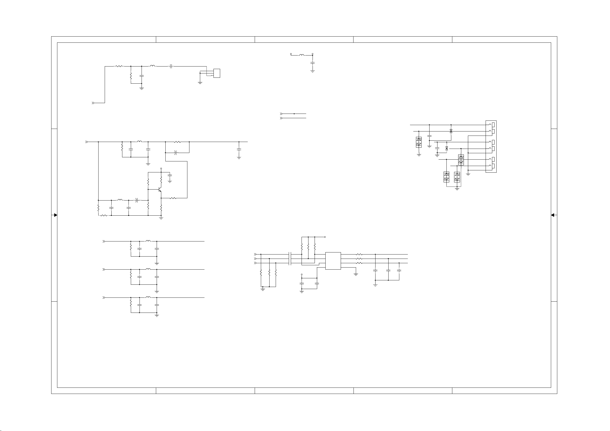
7-11
harman/kardon
BDT 2 / BDT 20 Service Manual
Page 33 of 37
7-11
A
Main Board Circuit Diagram:Video output&Spdif out
R451
R451
100R
100R
R450
R450
100R
100R
C452
C452
33pF
33pF
FB4520RFB452
0R
0.1uF
0.1uF
C451
C451
COAXOUT
B
CN10
CN10
1
2
3
COAX OUT
COAX OUT
C
FB450
FB450
VCC +5VV
FB/0805
FB/0805
C1053
C1053
10uF/10V
10uF/10V
0805-C
0805-C
D
E
4 4
ASPDIF
ASPDIF[5]
LOUT5[10]
ROUT5[10]
SPDIF OUTOUT
Y3-CY6
VCC
Q212
Q212
BT3904/NC
BT3904/NC
R454 0RR454 0R
CE606
CE606
470uF/16V/NC
470uF/16V/NC
CB968
CB968
0.1uF
0.1uF
R14030RR1403
0R
R456
R456
NC/0
NC/0
R1262
R1262
75 1%/NC
75 1%/NC
+
+
Y6[5]
R455
R455
75_1%R
75_1%R
L451 1.8uHL451 1.8uH
C455
C455
47pF
47pF
C456
C456
47pF
47pF
3 3
R1398
R1398
2.4K/NC
2.4K/NC
L852
R535
R535
100R_1%/NC
100R_1%/NC
C509
C509
10pF/NC
10pF/NC
R536
R536
91_1%/NC
91_1%/NC
L852
1.2uH/NC
1.2uH/NC
C510
C510
10pF/NC
10pF/NC
CE605
CE605
47uF/16v /NC
47uF/16v /NC
+
+
R1399
R1399
1.2K/NC
1.2K/NC
CVBS
CB1009
CB1009
33pF/NC
33pF/NC
FL
FR
COMPONENT
FR
R/V
C626
C626
100PF
100PF
D5D5
2 1
Right (Red)
INA-1KV
INA-1KV
TVS4
TVS4
FL
B/U
C627
C627
100PF
100PF
INA-1KV
INA-1KV
TVS3
TVS3
CVBS
G/Y
D7D7
2 1
Left (White)
PB (Blue)
D8D8
CVBS (Yellow)
Y (Green)
2 1
D6D6
2 1
Pr (Red)
J6
RCA-6J6RCA-6
8
9
1
6
7
2
4
5
3
Y2
Y2[5]
R461
R461
75_1%R
75_1%R
L453 0.22uHL453 0.22uH
C459
C459
C460
C460
22pF
22pF
22pF
22pF
2 2
Y3
Y3[5]
Y1
Y1[5]
R467
R467
75_1%R
75_1%R
R470
R470
75_1%R
75_1%R
L455 0.22uHL455 0.22uH
C464
C464
C463
C463
22pF
22pF
22pF
22pF
L450 0.22uHL450 0.22uH
C466
C466
C465
C465
22pF
22pF
22pF
22pF
G/Y
Y2[5]
Y3[5]
Y1[5]
B/U
R/V
150R/NC
150R/NC
R1354
R1354
R1355
R1355
150R/NC
150R/NC
R1356
R1356
150R/NC
150R/NC
C608
C608
0.1uF/NC
0.1uF/NC
16V
16V
C609
C609
0.1uF/NC
0.1uF/NC
16V
16V
C610
C610
0.1uF/NC
0.1uF/NC
16V
16V
1 2
1 2
1 2
10%
10%
10%
10%
10%
10%
R1348
R1348
7.5MR/NC
7.5MR/NC
+5VV
0805-C
0805-C
R1349
R1349
7.5MR/NC
7.5MR/NC
C607
C607
10uF/10V
10uF/10V
R1350
R1350
7.5MR/NC
7.5MR/NC
C1002
C1002
0.1uF
0.1uF
+5VV
U913
U913
1
IN1
2
IN2
3
IN3
VCC4GND
FMS6363CS/NC
FMS6363CS/NC
OUT1
OUT2
OUT3
R1343 75 1%/NCR1343 75 1%/NC
8
R1345 75 1%/NCR1345 75 1%/NC
7
R1347 75 1%/NCR1347 75 1%/NC
6
5
C1006
C1006
33PF/NC
33PF/NC
C1007
C1007
33PF/NC
33PF/NC
R/V
B/U
G/Y
C1008
C1008
33PF/NC
33PF/NC
1 1
A
B
C
D
E
Page 34

7-12
harman/kardon
BDT 2 / BDT 20 Service Manual
Page 34 of 37
7-12
A
-12V
-12V[2]
+12V
+12V[2,13]
3.3V
3.3V[2,3,5,6,7,8,11,12,13]
SCL
SCL
SDA
SDA
CSN
R1388 NC/0RR1388 NC/0R
AOMCLK_R
1 1
5V_STBY
R1389 NC/0RR1389 NC/0R
AL
AOUTL-
C168
C168
+
+
NC/10uF/16V
NC/10uF/16V
R75
R75
4.7K/NC
21
CSN
AL
ARAOBCK_R
5V_STBY
R122
R122
NC/10K
NC/10K
1%4.7K/NC
1%
2 2
R79
R79
1%
1%
4.7K/NC
4.7K/NC
AOUTL+
AR
AOUTR-
AOUTR+
3 3
4 4
CON14
CON14
4.7K/NC
XP8
XP8
R87
R87
C169
C169
+
+
NC/10uF/16V
NC/10uF/16V
R83
R83
4.7K/NC
4.7K/NC
1%4.7K/NC
1%
1
2
3
4
5
6
7
8
9
10
11
12
13
14
21
R135
R135
NC/10K
NC/10K
1%
1%
21
21
SCLSCL
SCL
SDA
AOMCLK
AOLRCK
AOBCK
AOSDATA0
AOSDATA1
AOSDATA2
AOSDATA3
MUTE
SDASDA
AOLRCKAOLRCK
VCC
Main Board Circuit Diagram:Audio DAC
R77
R77
5.1K/30K
1%5.1K/30K
1%
21
R78
12
C48
C48
3300PF/1000PF
3300PF/1000PF
21
R82
R82
5.1K/0R
5.1K/0R
12
C66
C66
3300PF/1000PF
3300PF/1000PF
21
C69
C69
0.1uF
0.1uF
R90
R90
5.1K/0R
5.1K/0R
1%
1%
470R/5.1K
MUTE1MUTE1
R78
1%
1%
470R/5.1K
AOMCLKAOMCLK
1%470R/5.1K
1%
R86
R86
21
470R/0R
470R/0R
1%470R/5.1K
1%
21
470R/0R
470R/0R
AOBCKAOBCK
AOSDATA0AOSDATA0
AOSDATA1AOSDATA1
AOSDATA2AOSDATA2
AOSDATA3AOSDATA3
MUTEMUTE
R81
R81
5.1K/30K
R89
R89
C59
C59
1 2
560PF/100PF
560PF/100PF
1%
1%
21
R85
R85
1%5.1K/30K
1%
21
C63
C63
1 2
560PF/100PF
560PF/100PF
1%
1%
21
12
NE5532D
NE5532D
12
6
5
-12VA
SO8
SO8
U6B
U6B
SO8
SO8
2
3
ININ+
+12VA
C62
C62
470PF/NC
470PF/NC
ININ+
U6A
U6A
C64
C64
470PF/NC
470PF/NC
4
NE5532D
NE5532D
V-
OUT
V+
8
-12VA
4
OUT
8
+12VA
7
V-
V+
B
OP CIRCUIT
C60
C60
0.1uF
1
0.1uF
0.1uF
0.1uF
C61
C61
-12V[2]
+12V[2,13]
+12V
AOUTL
AOUTL
R59
C68
C68
0.1uF
0.1uF
0.1uF
0.1uF
R59
100R
100R
-12VA
C67
C67
R62
R62
100R
100R
+12VA
R97
R97
100R
100R
-12V
CE18
CE18
+
+
100uF/16V
100uF/16V
R98
R98
100R
100R
CE17
CE17
+
+
100uF/16V
100uF/16V
AOUTR
for inside and outside Audio DAC
AOSDATA3 [5]
AOSDATA2 [5]
AOSDATA1 [5]
AOSDATA0 [5]
AOLRCK [5]
AOBCK [5]
DAC_RST#
AOMCLK [5]
DAC_RST# [6]
C501
C501
10uF/16V
10uF/16V
MUTE_L
+
+
C511
C511
+
+
10uF/16V
10uF/16V
DAC_RST#
+12V_P
AOMCLK_R[5]
AOBCK_R[5]
AOSDATA4_R[5]
AOLRCK_R[5]
R1362 330RR1362 330R
R501
R501
470R
470R
R504
R504
100K
100K
R512
R512
470R
470R
R514
R514
100K
100K
MUTE_R
R507
R507
3.3K
3.3K
C
R516
R516
3.3K
3.3K
C613
C613
0.01uF
0.01uF
R1358 100RR1358 100R
R1359 100RR1359 100R
D
OUTSIDE DAC
U914
U914
78L05
78L05
3
OUT
IN
C611
+
+
U915
U915
1
MCLK
2
BICK
3
SDTI1
4
LRCK
5
PDN
6
CSN
CCLK7AOUTR+
8
CDTI
AK4385ET
AK4385ET
C611
0.1uF
0.1uF
DZFL
DZFR
AOUTL+
AOUTLAOUTR-
VDD
VSS
CE603
CE603
10uF/10V
10uF/10V
CSN
SCL
SDA
GND
2
MUTE_1
16
MUTE_2
15
14
13
AOUTL+
12
AOUTL-
11
AOUTR+
10
AOUTR-
9
1
L859 100uHL859 100uH
C612
C612
0.1uF
0.1uF
C625
C625
10uF
10uF
C628
C628
0.1uF
0.1uF
R1367
R1367
0R/NC
0R/NC
VCC_P5V_STBY
R13640RR1364
0R
MUTE CIRCUIT
R1361
R1361
10K
R1368
R1368
22K
22K
R1366
R1366
4.7K
4.7K
Q215
Q215
BT3904
BT3904
R1391
R1391
10K
220U/16V
220U/16V
R1383
R1383
100K
100K
CE597
CE597
100K
100K
Q219
Q219
3906
3906
R502
R502
470R
470R
Q17
Q17
BT3904
BT3904
Q16
Q16
BT3904
BT3904
R513
R513
470R
470R
Q18
Q18
BT3904
BT3904
ROUT5AOUTR
Q19
Q19
BT3904
BT3904
LOUT5
R508
R508
3.3K
3.3K
ROUT5 [9]
R517
R517
3.3K
3.3K
LOUT5 [9]
MUTE_L
MUTE_R
R1363
R1363
3.3K
3.3K
R1365
R1365
4.7K
D525
AMUTE[5,7]
A_MUTE_M[7]
D525
1N4148
1N4148
D526
D526
1N4148/NC
1N4148/NC
4.7K
MUTE_1
MUTE_2
VCC_P
R13841KR1384
1K
R13961KR1396
1K
Q218
Q218
3906
3906
Q213
Q213
3906
3906
R1360
R1360
4.7K
4.7K
+
+
MUTE_L
MUTE_R
E
Q214
Q214
3906
3906
MUTE
D523
D523
D524
D524
1N4148
1N4148
1N4148
1N4148
A
B
C
D
E
Page 35

7-13
harman/kardon
BDT 2 / BDT 20 Service Manual
Page 35 of 37
7-13
5
Main Board Circuit Diagram:SMSC 8700
3.3V
3.3V[2,3,5,6,7,8,10,12,13]
R701NCR701
NC
R707NCR707
NC
0.1uF
0.1uF
C712
C712
R741
R741
10K/NC
10K/NC
ETRXER
ETCRS
LAN-3.3V
LAN-3.3V
C711
C711
22uF/10v
22uF/10v
R735
R735
10K
10K
LAN0_RESET#
C716
C716
0.1uF
0.1uF
ETMDIO[7]
ETMDC[7]
ETRXD3[7]
ETRXD2[7]
ETRXD1[7]
ETRXD0[7]
ETRXDV[7]
ETRXCLK[7]
ETRXER[7]
ETTXEN[7]
ETTXCLK[7]
ETTXD0[7]
ETTXD1[7]
ETTXD2[7]
ETTXD3[7]
ETCOL[7]
ETCRS[7]
R727 1MR727 1M
Y700
Y700
25.0000MHz
25.0000MHz
C700
C700
22PF
22PF
R700 33RR700 33R
R708 33RR708 33R
R7090RR709
R710 0RR710 0R
R7110RR711
R712 0RR712 0R
R713 0RR713 0R
R714 0RR714 0R
R715 0RR715 0R
R716 0RR716 0R
R717 0RR717 0R
R718 0RR718 0R
R719 0RR719 0R
R720 0RR720 0R
R7210RR721
R722 0RR722 0R
R7230RR723
R20
R20
10R
10R
C715
C715
22PF
22PF
0R
0R
0R
0R
LAN0_ETMDIO
LAN0_ETMDC
LAN0-ETRXD3
LAN0-ETRXD2
LAN0-ETRXD1
LAN0-ETRXD0
LAN0-ETRXDV
LAN0-ETRXCLK
LAN0-ETRXER
LAN0-ETTXCLK
LAN0-ETTXD0
LAN0-ETTXD1
LAN0-ETTXD2
LAN0-ETTXD3
LAN0-ETCOL
LAN0-ETCRS
D D
FB701
FB701
FB/0805/NC
3.3V_STBY
3.3V
C C
FB/0805/NC
FB705
FB705
FB/0805
FB/0805
Resert-NET[2,7]
C701
C701
0.1uF
0.1uF
LAN0_RESET#
4
C702
C702
0.1uF
0.1uF
U701
U701
16
MDIO
17
MDC
8
RXD3/PAYAD2
9
RXD2/RMIISEL
10
RXD1/MODE1
11
RXD0/MODE0
26
RXDV
7
RX_CLK/PHYAD1
13
RX_ER/RXD4
21
TXEN
20
TXCLK
22
TXD0
23
TXD1
24
TXD2
25
TXD3
15
COL/CRS_DV/MODE2
14
CRS
19
NRST
5
CLKIN/XTAL1
4
XTAL2
SMSC8710
SMSC8710
C703
C703
0.1uF
0.1uF
12
VDDIO
32
27
VDD2A1VDD1A
LED1/REGOFF
LED2/NINTSEL
Nint/TX_ER/TXD4
RBIAS
R731
R731
12.4K_1%
12.4K_1%
FB700
FB700
FB/0603
FB/0603
VDDCR
33
RXN
VSS/FLAG
RXP
TXN
TXP
LAN-3.3V
C704
C704
0.1uF
0.1uF
30
31
28
29
3
2
18
6
C705
C705
0.1uF
0.1uF
TP_RX-
TP_RX+
TP_TXTP_TX+
LINKLED
ACTIVITYLED
LED4/PHYAD4
VDD_CORE
C713
C713
0.1uF
0.1uF
C706
C706
10pF
10pF
C708
C708
10pF
10pF
C714
C714
4.7uF
4.7uF
LAN-3.3V
C709
C709
10pF
10pF
ACTIVITYLED
LINKLED
C707
C707
10pF
10pF
R1404
R1404
49.9R
49.9R
0603-R
0603-R
3
R1405
R1405
49.9R
49.9R
0603-R
0603-R
TDK ACM2012H-900-2P/0
TDK ACM2012H-900-2P/0
TDK ACM2012H-900-2P/0
TDK ACM2012H-900-2P/0
LAN-3.3V
R734 330RR734 330R
R738 330RR738 330R
TPTXTPTX+
R1312
R1312
49.9R
49.9R
0603-R
0603-R
R1299 0R/NCR1299 0R/NC
1
L860
L860
DLW21SN900SQ2L-2
DLW21SN900SQ2L-2
2
L861
L861
DLW21SN900SQ2L-2
DLW21SN900SQ2L-2
R1314
R1314
49.9R
49.9R
0603-R
0603-R
LAN-3.3V
3
41
LAN-3.3V
ACTIVITYLED
LINKLED
R1294
R1294
10R
10R
0805-R
0805-R
R1296 0RR1296 0R
R1300 0RR1300 0R
C595
C595
0.22uF
0.22uF
RD-
4
32
TD+
TD+
TD-
R1334 330RR1334 330R
R1335 330RR1335 330R
RD+
PWFBOUT2VDD_CORE
PWFBOUT1
2
J1
J1
1
3
2
RJ-45
RJ-45
7
6
13
8
14
4
15
5
16
9
G
G
10
12
Y
Y
11
KS-06
KS-06
1
LAN-3.3V
R736 10K/NCR736 10K/NC
LAN0_ETMDIO
LAN0-ETRXD0
LAN0-ETRXD1
LAN0-ETRXD2
LAN0-ETRXD3
LAN0-ETCOL
LAN0-ETRXCLK
B B
R739 10K/NCR739 10K/NC
R740 10K/NCR740 10K/NC
R702 10KR702 10K
R742 10KR742 10K
R743 10KR743 10K
R746 10KR746 10K
R747 10K/NCR747 10K/NC
R748 10K/NCR748 10K/NC
R750 10K/NCR750 10K/NC
R751 10K/NCR751 10K/NC
R752 10KR752 10K
R753 10K/NCR753 10K/NC
LAN-3.3V
R744NCR744
NC
LAN0-ETCRS
LED4/PHYAD4
R749
R749
10K
10K
R745NCR745
NC
A A
5
4
3
2
1
Page 36

7-14
harman/kardon
BDT 2 / BDT 20 Service Manual
Page 36 of 37
7-14
5
Main Board Circuit Diagram:MT1939E-128/SATA
USFCS#FE_SFCS#
FE_SFDO USFDO
FE_SFCLK USFCK
USFDIFE_SFDI
D D
XP6
XP6
C C
46
FE_GND
47
FE_GND
VCC_CLSFT
FE_GND
GND_CLSFT
TOP
TOP
SW(DVD/CD)
MON_CD/DVD
SEL_HFA_DVD
B B
SEL_HFA_CD
HEADER 45 SMD0.5 TOP
HEADER 45 SMD0.5 TOP
VCC_HFM AVCC
FE_GND
VRDC2O
3.3V[2,3,5,6,7,8,10,11,13]
FCS2+
FCS2-
TRK+
FCS1+
TRK-
FCS1-
SIG_P0
SW3(BD)
SWB2(BD)
SWB1(BD)
VREF_PD
VCC_+5PD
GND_PD
GND1
LDI_BD
LDI_CD
LDI_DVD
GND1
TEMP
VCC(HFM)
MON_BD
SEL_DVD
SEL_CD
GND1
F_C95
F_C95
2.2uF
2.2uF
3.3V
F_NC13F_NC13
F_NC14F_NC14
F_NC25F_NC25
M
1
2
3
4
5
6
7
A-
8
B-
9
A+
10
B+
11
12
13
14
A
15
B
16
C
17
D
18
SA
19
SB
20
SC
21
SD
22
23
RF+
24
RF-
25
26
27
28
29
30
31
32
33
34
35
36
37
38
39
40
41
42
43
44
45
NC
FE_GND
F_NC22F_NC22
F_R125 NCF_R125 NC
FNIP
RFO+
RFO-
VHAVC
VCC_HFM
FE_GNDFE_GND
FE_GND
F_Q15
F_Q15
BT3904
BT3904
GIO7
F_R150 NCF_R150 NC
F_R126 0RF_R126 0R
RFO+RFO+
VHAVCVHAVC
BD_LD
CD_LD
DVD_LD
VCC_HFMVCC_HFM
MDI_DVD
MDI_BD
DVD_VR
CD_VR
DVD_HFM
CD_HFM
F_R1411KF_R141
1K
F_R147 470RF_R147 470R
F_R142
F_R142
470R
470R
FE_GND
FE_GND
FOC2+
FOC2-
TR-
FOC1+
TR+
FOC1CO_ACO_BCO_A+
CO_B+
INB
INA
IND
INC
ING
INH
INF
INE
LGO2P
RFO-RFO-
LGO3P
LGO3N
VCC_PDIC
GAINSW
AUX1
add for large current
F_C111
F_C111
10uF
10uF
USFCS# [6]
USFDO [6]
USFCK
USFDI [6]
A3.3V
A1.2V
F_C121
F_C121
0.1uF
0.1uF
FE_GND
A3.3V
FOC2+FOC2+
FOC2-FOC2-
TR-TR-
FOC1+FOC1+
TR+TR+
FOC1-FOC1-
A3.3V
GIO71GIO71
INBINB
INAINA
F_C135NCF_C135
NC
INDIND
INCINC
INGING
INHINH
FE_GND
INFINF
INEINE
LGO3PLGO3P
LGO3NLGO3N
VCC_PDICVCC_PDIC
BD_LDBD_LD
CD_LDCD_LD
DVD_LDDVD_LD
MDI_DVDMDI_DVD
MDI_BDMDI_BD
DVD_VRDVD_VR
CD_VRCD_VR
DVD_HFMDVD_HFM
CD_HFMCD_HFM
F_R146
F_R146
33R
33R
F_Q16
F_Q16
2SB1132
2SB1132
F_L9 10uHF_L9 10uH
FNIP
[6]
A1.2V
CO_A-CO_A-
CO_B-CO_B-
GAINSWGAINSW
CO_A+CO_A+
CO_B+CO_B+
A3_3VA3_3V
LGO2PLGO2P
FE_GND
A3.3V
FE_GND
F_R140
F_R140
33R
33R
RFORFO+
RFO+
RFO-
F_C120
F_C120
2.2uF
2.2uF
A A
FE_GND
A1.2V
A3.3V
F_R149
F_R149
10K
10K
AUX1AUX1
F_C134
F_C134
0.1uF
0.1uF
DVD_LD
F_C133
F_C133
0.1uF
0.1uF
F_C114 0.1uFF_C114 0.1uF
F_C115 0.1uFF_C115 0.1uF
FOIP
FOIN
MDI_DVD
MDI_BD
F_C1120.1uFF_C1120.1uF
F_C1130.1uFF_C1130.1uF
F_C1180.1uFF_C1180.1uF
F_C1170.1uFF_C1170.1uF
F_C1160.1uFF_C1160.1uF
F_C110
F_C110
0.1uF
0.1uF
FE_GND
VRDC3O
VDAC0
A1.2V
V14REF
VFVREF
VHAVC
TRINA
TRINB
TRINC
TRIND
INA
INB
INC
IND
INE
INF
ING
INH
FE_GND
F_Q14
F_Q14
BT3904
BT3904
FE_GND
F_C17
F_C17
0.1uF
0.1uF
F_R50 22K/1%F_R50 22K/1%
FE_XTALI
U7
N5
J1
W5
P4
R5
N3
R7
P2
N1
R3
T6
U9
V6
U1
R1
T2
W7
V2
U3
P8
T4
U5
Y4
Y2
W1
W3
V4
AA7
W9
AB8
AC7
F_R1431KF_R143
1K
F_R144
F_R144
470R
470R
XTAL25MO
U100G
U100G
FE_V14
FE_VFVREF
FE_HAVC
FE_AGND
FE_TRINA
FE_TRINB
FE_TRINC
FE_TRIND
FE_INA
FE_INB
FE_INC
FE_IND
FE_AVDD33_2
FE_INE
FE_INF
FE_ING
FE_INH
FE_AGND
FE_FOIP
FE_FOIN
FE_AVDD12_1
FE_FPDODVD
FE_FPDOCD
FE_RFIN
FE_RFIP
FE_RFIP2
FE_RFIN2
FE_REG_CAP
FE_AGND
FE_AVDD33_3
FE_AVDD12_3
FE_AVDD12_4
FE_GND
F_Q13
F_Q13
BT3904
BT3904
FE_GND
F_R148 470RF_R148 470R
4
F_R51
F_R51
1.2K/1%
1.2K/1%
EQBIAS
AA9
AJ1
K4
AJ3
FE_EQBIAS
FE_XTAL25MI
FE_XTAL25MO
FE_AVDD33_LVDS
FE_SAGND
FE_LVDS_1P
FE_LVDS_1NY6FE_LVDS_2P
FE_LVDS_2N
AA5
AA1
AA3
AN5
LGO1N
LGO2P
LGO2N
LGO1P
F_C122 0.1uFF_C122 0.1uF
VCC_BD_LD
F_R1181KF_R118
1K
F_R117 470RF_R117 470R
F_R119
F_R119
470R
470R
F_C104
F_C104
10uF
10uF
F_C14 0.1uFF_C14 0.1uF
VDAC0
AUX1
VRDC3O
M4
L3
FE_AUX1
FE_VDAC0
FE_VWDC3OL1FE_VWDC2OM2FE_VWDC1O
FE_LVDS_3P
FE_LVDS_3N
FE_LVDS_4P
AB4
AC3
AC1
LGO3P
LGO3N
LGO4P
FE_GND
VRDC1O
VRDC2O
FE_LVDS_4N
AB2
LGO4N
LGO5P
F_C98
F_C98
10uF
10uF
VCC_LD
M3.3V
D1.2V
RSTI
MPX1
MPX2
MPX3
VRDCO
M6
L5
K2
J3
T10
G1
M10
R9
P6
FE_RSTI
FE_VRDC0
FE_MVDDQ
FE_DVDD12I
FE_MPXOUT1
FE_MPXOUT2
FE_MPXOUT3
FE_AVDD12_2
FE_LVDS_5P
FE_LVDS_5N
FE_AVDD33_4
FE_CFREQ
FE_OSCEN
FE_CMOD
FE_GAINSW1
FE_GAINSW2
FE_GAINSW3
V8
AF8
AB6
AE7
AE5
AC5
AD2
AD6
AG5
LDD_SDIO
LDD_CLK
LDD_SEN
LGO5N
GAINSW
GAINSW2
GAINSW3
add for large current
F_R120
F_R120
39R
39R
F_Q11
F_Q11
2SB1132
2SB1132
F_L8
F_L8
10uH
10uH
F_R145
F_R145
F_R122
F_R122
33R
33R
33R
33R
F_Q17
F_Q17
2SB1132
2SB1132
add for large current
F_L10 10uHF_L10 10uH
D3.3V
D1.2V
M3.3V
GIO15
H2
U11
M8
AB12
FE_MVDDQ
FE_DVDD12I
FE_DVDD33O
FE_FMO3
FE_FMO4
FE_TLO
AF6
AH6
AG7
AM8
TLO
TRO
FMO4
FMO3
A3.3V
F_R121
F_R121
39R
39R
BD_LD
CD_LD
GIO14
GIO19
GIO16
GIO17
GIO18
FE_SFWP#
AW1
H6
G7
AW3
L7
AV2
FE_JTDI
FE_JTDO
FE_JTMS
FE_JTCLK
FE_SFWP#
FE_JTRST#
FE_JRTCLK
FE_TRO
FE_FOO
FE_TRAYPWM
FE_FMO
FE_FMO2
FE_DMO
FE_DVDD12I
Y10
AF4
AF2
AE3
AE1
AD4
FOO
TYPWM
FMO
FMO2
DMO
D1.2V
VCC_PDIC
VCC_LD
VHAVC V14REF VFVREF
FE_GND
FE_SFDO
FE_SFCLK
FE_SFHOLD
FE_SFCS#
FE_SFDI
K6
C1
F2
F4
E1
FE_SFDI
FE_SFDO
FE_SFCS#
FE_SFCLK
FE_DVDD33ON7FE_DVDD33O
FE_DVDD33O
FE_GIO12
AE9
AC9
AT10
AB10
FE_GND
GIO12
GIO13
D3.3V
D3.3V
D3.3V
TP54TP54
SPLLVDD
F_C102
F_C102
2.2uF
2.2uF
SXVDD
F_C103
F_C103
2.2uF
2.2uF
VCC_BD_LD
F_C101
F_C101
2.2uF
2.2uF
D1.2V
W11
T8
FE_DVDD12I
FE_DVDD12I
FE_SFHOLD#
FE_FG
FE_GIO2
FE_GIO11
FE_GIO10
FE_GIO9
FE_GIO8
FE_GIO7
FE_GIO6
FE_GIO5
FE_GIO4
FE_AVDD12_RX
FE_SRXP
FE_SRXN
FE_STXN
FE_STXP
FE_STXVDD12
FE_SPLLVDD12
FE_SVDD33
FE_SXVDD33
FE_PLAY#
FE_LIMIT
FE_DVDD12I
FE_GIO3
FE_EJECT#
FE_TRAYOUT
FE_TRAYIN#
FE_GIO1
FE_GIO0
FE_FSOURCE
FE_DVDD33O
FE_DVDD33O
FE_DVDD33O
FE_GIO13
FE_AGND
MT8530_DDR2
MT8530_DDR2
Y8
TP53TP53
F_R123 4.7RF_R123 4.7R
F_R124 4.7RF_R124 4.7R
F_C105
F_C105
2.2uF
2.2uF
FE_GND
F_C107
F_C107
2.2uF
2.2uF
FE_GND
F_C100
F_C100
F_C99
F_C99
2.2uF
2.2uF
2.2uF
2.2uF
M
FE_GND
A1.2V
A3.3V
F_C106
F_C106
2.2uF
2.2uF
G3
E3
D2
H8
E5
L9
G5
G9
J5
J7
AP8
AR1
AR3
AP2
AN1
AP6
AN7
AL7
AM6
AH2
AG3
V10
AG1
AH4
AK4
AJ5
AG9
AD8
AH8
N11
N9
P10
FE_GND
F_NC26F_NC26
F_NC27F_NC27
2 3
FE_GND
F_NC28F_NC28
3
FG
GIO2
UTXD
URXD
GIO9
GIO8
GIO7
GIO6
GIO5
GIO4
RXIP
RXIN
TXON
TXOP
SPLLVDD
SXVDD
PLAY#
LED1
EJECT#
TRAYOUT#
TRAYIN#
MUTE2
MUTE1
F_Q12
F_Q12
2SK3018
2SK3018
1
2 3
A3.3V
F_R128
F_R128
12K/NC
12K/NC
F_R116 1KF_R116 1K
F_Q18
F_Q18
2SK3018
2SK3018
1
5V_STBY[2,5,10]
5V_STBY
F_C109
F_C109
TP7TP7
D3.3V
FE_GND
DVD_VR
F_R151 1KF_R151 1K
AVCC
VCC_OPU
F_C108NCF_C108
NC
FE_GND
PLAY#[13]
GIO8[13]
LGO4N[13]
LED1[13]
UTXD[13]
EJECT#
GIO2
URXD
5V_STBY
AVCC
F_R49
F_R49
20K/NC
20K/NC
F_R48
F_R48
10K
10K
FE_GND
A1.2V
0.1uF
0.1uF
A1.2V
SPLLVDD
SXVDD
D1.2V
TRAYOUT# [13]
TP8TP8
F_C119
F_C119
0.1uF
0.1uF
CD_VR
GAINSW
LGO1P
PLAY#
GIO8
LGO4N
LED1
UTXD
URXD [13]
F_R47
F_R47
20K
20K
R461KR46
RSTI1
F_C20
F_C20
0.1uF/NC
0.1uF/NC
F_C131
F_C131
0.1uF
0.1uF
EJECT# [13]
GIO2 [13]
2
TXOP
TXON [6]
RXIN [6]
RXIP [6]
3.3V
URXD
UTXD
FE_GND
TRAYIN#
FG
VFVREF
VHAVC
GIO6
EJECT#
LED1
TP44TP44
TP45TP45
TP46TP46
TP47TP47
TP48TP48
TP49TP49
TP50TP50
TP52TP52
TP423TP423
F_C33
F_C33
0.1uF
0.1uF
A3.3V
TP37TP37
TP38TP38
TRINA
TP39TP39
TRINB
TP40TP40
TRINC
TP41TP41
TRIND
TP42TP42
FOIP
TP43TP43
FOIN
VFVREF
LDD_SDIO
LDD_CLK
LDD_SEN
GIO4
GIO5
GIO6
GIO7
MPX3
GAINSW3
GIO8
GIO5
RSTI1
GAINSW2
[6]
A+1A+1
LGO2N
LGO3P
LGO1N
TP30TP30
TP31TP31
LGO1N
TP32TP32
LGO2N
TP33TP33
LGO3P
TP34TP34
LGO3N
TP35TP35
LGO4P
TP36TP36
LGO5P
LGO5N
1K
RSTI
GIO17
GIO17
GIO18
GIO18
VRDCO
TP6TP6
VRDC1O
TP5TP5
TXOP
TXON
GIO9
F_R59 0RF_R59 0R
MPX1
F_R70 0RF_R70 0R
MPX2
F_R113 0RF_R113 0R
FE_GND
F_R114
F_R114
100K
100K
FE_XTALI
F_R115 0RF_R115 0R
V14REF
F_C1231000pFF_C1231000pF
F_C1291000pFF_C1291000pF
F_C1242200pFF_C1242200pF
F_C1260.1uFF_C1260.1uF
F_C1272200pFF_C1272200pF
M
F_C125330pFF_C125330pF
F_C130NCF_C130NC
F_R129 NCF_R129 NC
GIO17
GIO18
F_C128330pFF_C128330pF
F_C132330pFF_C132330pF
TR+[13]
TR-[13]
FOC1-[13]
FOC1+[13]
FOC2-[13]
FOC2+[13]
TLSO[13]
TRAYPWM[13]
V14REF[13]
MUTE2[13]
MUTE1[13]
RSTI1[6,13]
USFCK[6]
USFDO[6]
USFCS#[6]
USFDI[6]
NS_CLKIN_33 [5]
NS_RFIP [5]
NS_RFIN [5]
F_C93NCF_C93
NC
XTAL25MO
25M_Buf [6]
TYPWM
R96 0RR96 0R
R815 0RR815 0R
R823 0RR823 0R
FMO4
FMO3
DMO
FMO2
TRO
FOO
TLO
FMSO[13]
FMSO2[13]
DMSO[13]
FOSO[13]
TRSO[13]
CO_B-[13]
CO_B+[13]
CO_A+[13]
CO_A-[13]
FMSO4[13]
FMSO3[13]
R819NCR819
NC
FMSO4
F_R133 20KF_R133 20K
FMSO3
F_R130 20KF_R130 20K
FMSO FMO
F_R138 10KF_R138 10K
DMSO
F_R134 10KF_R134 10K
FMSO2
F_R131 10KF_R131 10K
TRSO
F_R137 10KF_R137 10K
FOSO
F_R135 10KF_R135 10K
TLSO
F_R136 10KF_R136 10K
TRAYPWM
F_R132 10KF_R132 10K
TR+
TRFOC1FOC1+
FOC2FOC2+
TLSO
TRAYPWM
V14REF
MUTE2
MUTE1
RSTI1
USFCK
USFDO
USFCS#
USFDI
A3.3V
GIO14 TTRST#A
GIO19 TTDOA
GIO16 TTMSA
GIO17
GIO18
GIO15 TTDIA
add 8pin socket
Servo debug
FE_SFWP#
FE_SFHOLD
FMSO
FMSO2
DMSO
FOSO
TRSO
CO_BCO_B+
CO_A+
CO_AFMSO4
FMSO3
/TRST
TDO
TMS
TCK
RTCK
TDI
/NRST
R818NCR818
NC
RXIN
RXIP
XP7
XP7
1
2
3
4
4x1 W/HOUSING
4x1 W/HOUSING
F_R58
F_R58
10K
10K
F_R57 0RF_R57 0R
F_R139 10KF_R139 10K
F_R152 0RF_R152 0R
TRAYIN#[13]
FG[13]
VFVREF
VHAVC[13]
GIO6[13]
EJECT#[13]
LED1[13]
TTRST#A
TTDIA
TTCKA
TRTCKA
TTMSA
TTCKA
TRTCKA
TTDOA
Default:R325=NC,R335=10K
ICE=R325=10KˈR335=NC
UTXD
URXD
LGO3N
LGO4P
LGO5P
LGO5N
˗
1
GIO8 [13]
GIO5 [13]
RSTI1 [6,13]
GAINSW2 [13]
UTXD1UTXD1
UTXD [13]
URXD [13]
URXD1URXD1
JTAG Port
HA1
HA1
10
9
8
TOP
TOP
7
6
5
4
3
2
1
HEADER 8 SMD1.0 TOP
HEADER 8 SMD1.0 TOP
CON1.25-8-SMT-XP
CON1.25-8-SMT-XP
5
4
3
2
1
Page 37

7-15
harman/kardon
BDT 2 / BDT 20 Service Manual
Page 37 of 37
7-15
A
B
C
D
E
Main Board Circuit Diagram:Power regulator
VCC
F_FB1 0RF_FB1 0R
4 4
3 3
F_CE15
F_CE15
+
+
100uF/16V
100uF/16V
+12V
F_FB3 0RF_FB3 0R
F_NC1F_NC1
F_NC3F_NC3
F_NC4F_NC4
F_NC2F_NC2
F_NC5F_NC5
F_FB2 0RF_FB2 0R
FE_GND
AVCC
MVCC
M12V
M
AVCC
F_CE12
F_CE12
+
F_C75
F_C75
4.7uF
4.7uF
+
F_C62
F_C62
100uF/16V
100uF/16V
0.1uF
0.1uF
FE_GND
VHAVC
V14REF
F_C81
F_C81
F_C80
F_C80
2.2uF
2.2uF
2.2uF
2.2uF
FE_GNDFE_GND
F_C66
F_C66
F_C67
F_C67
4.7uF
4.7uF
M3.3V D1.2V
F_C76
F_C76
0.1uF
0.1uF
0.1uF
0.1uF
F_C72
F_C72
F_C77
F_C77
10uF/10v
10uF/10v
F_C68
F_C68
0.1uF
0.1uF
0.1uF
0.1uF
D3.3V
F_C73
F_C73
0.1uF
0.1uF
F_C136
0.1uF
0.1uF
F_C74
F_C74
0.1uF
0.1uF
MVCC
F_CE17
F_CE17
+
+
220uF/16V
220uF/16V
M
V14REF
V14REF
DMSO
FMSO
FMSO2
A3.3V
M
10uF/16V
10uF/16V
M
F_C79
F_C79
10uF
10uF
M12V
F_CE13
F_CE13
F_R96 10KF_R96 10K
F_R97 10KF_R97 10K
F_R99 15KF_R99 15K
F_R103
F_R103
F_C64
F_C64
0.1uF
0.1uF
F_R105 NCF_R105 NC
F_R106
F_R106
Motor Driver
Sensorless
F_U5
F_U5
1
SPIN
2
SL1IN
3
A+
A-
B+
B-
U
V
W
8
7
6
5
4
3
2
1
SL2IN
4
SPLIN
5
VM2
6
SL2+
7
GND
8
SL2-
9
SL1+
10
SL1-
11
GND
12
U
13
V
14
W
15
ACTFLG
16
COMMON
17
TEST
18
SLLIM
19
FG
20
EN1
21
EN2
R2A30209SP
R2A30209SP
M
A+
ABB+
U
V
W
F_R110 0RF_R110 0R
8.2K
8.2K
COMMON
10K
10K
FG
MUTE1
MUTE2
XP3
XP3
8x1 W/HOUSING
8x1 W/HOUSING
ACTRST
COMMON
REF
LOIN
FOIN
TOIN
TLIN
TLTL+
FO-
FO+
GND
5VCC
TO+
TO-
GND
LO-
LO+
VM3
STTH
SPGS
VM1
COMMONCOMMON
F_R98 10KF_R98 10KF_C136
F_R100 10KF_R100 10K
F_R101 10KF_R101 10K
TLTL+
FOFO+
TR+
TR-
LOADLOAD+
F_R107 0RF_R107 0R
F_R1080RF_R108
M
UU
VV
WW
F_C71
F_C71
0.1uF
0.1uF
F_R102 10KF_R102 10K
0R
F_CE14
F_CE14
+
+
220uF/16V
220uF/16V
F_R153NCF_R153
NC
M12V
42
41
40
39
38
37
36
35
34
33
32
31
30
29
28
27
26
25
24
23
22
A+A+
A-AB-BB+B+
TRAYPWM
FOSO
TRSO
TLSO
M
V14REF
F_C65
F_C65
0.1uF
0.1uF
M
F_C78
F_C78
10uF
10uF
F_C63
F_C63
0.1uF
0.1uF
M
F_R1090RF_R109
TRAYOUT#
TRAYIN#
LOAD+
LOAD-
LOAD-LOAD-
GND2GND2
M12V
MVCC
TRAYIN#TRAYIN#
TRAYOUT#TRAYOUT#
F_C85
F_C85
0.1uF
0.1uF
AGNDAGND
5PIN/2.0MM
5PIN/2.0MM
F_R104NCF_R104
NC
F_C70
F_C70
0.1uF
0.1uF
0R
M
1. Motor +
2. Motor -
3. GND
4. SW-2
5. SW-1
TRAYOUT#[12]
LOAD+LOAD+
TL-
R283
R283
10K
LGO4N
LED1
GIO2
UTXD
URXD
F_C82NCF_C82
10K
PLAY#
EJECT#
GIO8
U
V
W
NC
VCC
PLAY#PLAY#
EJECT#EJECT#
GIO8GIO8
VCCVCC
LGO4NLGO4N
LED1LED1
GIO2GIO2
UTXDUTXD
URXDURXD
5
4
3
2
1
XP4
XP4
FOC2+FO+
FOC2-FOFOC1+TL+
FOC1-
3.3V
R284
R284
10K
10K
XP5
XP5
1
2
3
4
5
6
7
8
9
10
10x1
10x1
CONS10-XP
CONS10-XP
F_C83NCF_C83
NC
F_C84NCF_C84
NC
M
GIO8
UTXD
URXD
TR+[12]
TR-[12]
FOC1-[12]
FOC1+[12]
FOC2-[12]
FOC2+[12]
TLSO[12]
TRAYPWM[12]
V14REF[12]
MUTE2[12]
MUTE1[12]
FMSO[12]
FMSO2[12]
DMSO[12]
FOSO[12]
TRSO[12]
CO_B-[12]
CO_B+[12]
CO_A+[12]
CO_A-[12]
FMSO4[12]
FMSO3[12]
TRAYIN#[12]
LGO4N[12]
GIO2[12]
PLAY#[12]
FG[12]
VFVREF[12]
VHAVC[12]
GIO6[12]
EJECT#[12]
LED1[12]
3.3V
TR+
TRFOC1FOC1+
FOC2FOC2+
TLSO
TRAYPWM
V14REF
MUTE2
MUTE1
FMSO
FMSO2
DMSO
FOSO
TRSO
CO_BCO_B+
CO_A+
CO_AFMSO4
FMSO3
TRAYIN#
LGO4N
GIO2
PLAY#
GIO8 [12]
UTXD [12]
URXD [12]
FG
VFVREF
VHAVC
GIO6
EJECT#
LED1
3.3V [2,3,5,6,7,8,10,11,12]
B+
TRAYIN#
F_C94
F_C94
0.1uF
0.1uF
(change to +9V)
VCC_OPU
F_C92
F_C92
10uF/16V
10uF/16V
F_C90
F_C90
1uF
1uF
F_U6
F_U6
APL1117-ADJ
APL1117-ADJ
OUT2IN
4
OUT
F_R111121R_1%F_R111121R_1%
F_R112 750R_1%F_R112 750R_1%
ADJ/GND
1
3
F_C91
F_C91
0.1uF
0.1uF
F_CE16
F_CE16
10uF/16V
10uF/16V
+12V
2 2
1 1
BAA+
F_C86NCF_C86
NC
F_C87NCF_C87
NC
F_C88NCF_C88
NC
M
F_C89NCF_C89
NC
+12V[2,10]
GIO5
GAINSW2
+12V
FMSO3
GIO6
FMSO4
A3.3V
PIN7:
GAINSW2 (GAINSW)
R772
R772
47K/NC
47K/NC
0603-R
0603-R
GAINSW2
R773
R773
47K/NC
47K/NC
0603-R
0603-R
M
GIO5 [12]
GAINSW2 [12]
A3.3V
MVCC
MVCC
PIN12:
GIO5 (VDAC0)
GIO5
F_C96 2.2uFF_C96 2.2uF
GAINSW2
FMSO4
FMSO3
R760 1KR760 1K
R761 33KR761 33K
R762 0RR762 0R
R764 33KR764 33K
F_C97
F_C97
1000pF
1000pF
M
MVCC
M
F_U7
F_U7
1
Vc
2
IN2
3
ENA
4
SOF
IN15GND
LB1848M/NC
LB1848M/NC
R754 1KR754 1K
R757 1KR757 1K
R758 1KR758 1K
R765 0RR765 0R
R766 0RR766 0R
MVCC
+
+
M
OUT4
OUT3
OUT1
OUT2
F_CE11
F_CE11
100uF/16V
100uF/16V
10
9
8
7
6
U703
U703
1
LED0
2
Latch_SET
3
Latch_CLR
4
SWR_SEQ1
5
SWR_SEQ2
6
SWR_OUTSEL/XMUTE
7
STEP_ENA
8
STP1_IN
9
STP2_IN
10
XLEDON
11
CSWON
12
COLLIENDZ
13
XRESET
14
A5V
15
AGND
M
TPC1391G4
TPC1391G4
M
Latch_RSOUT
Latch_XRSOUT
CSWI
CSWO
TEST1
FB3P3V
REG3P3V
PGND_SW
REG1PxV
P5V_SW
FB1PxV
STP2-
STP2+
STP1-
STP1+
COA+
COACOBCOB+
COLLIMATOR
MVCC
II
30
29
28
27
26
25
24
23
22
21
20
19
18
17
16
R1406NCR1406
NC
R14070R1407
0
M
COA-
R768 0RR768 0R
COA+
R769 0RR769 0R
COB-
R770 0RR770 0R
COB+
R771 0RR771 0R
M
CO_ACO_A+
CO_BCO_B+
A
B
C
D
E
Page 38

BDS + BDT Service guide. Harman/Kardon
Pairing loader and main board.
Make sure to read the entire process, before starting.
This software procedure allows you to replace a loader or a main board in the following
products:
BDS 2/230
BDS 5/230
BDT 20/230
IMPORTANT: This update must be performed in an ESD protected environment!
1.
To perform this upgrade, the following equipment is needed:
PC with a USB port.
BDx Service KIT:
USB cable-JIG, a few loose 4pin connectors)
Software package incl drivers:
IP:ftp2.harman.com
Login: ServiceLevel2 , Password: s3rv1c3L
Direct access with a web browser:
ftp://servicelevel2:s3rv1c3L@ftp2.harman.com/Service/Level2
2D Scanner. IPhone, Android and other smart phones can
be used instead: Phones must be able to read 2D bar codes.
2D code sample below
1B.
First time only: Install the BDx service kit drivers (PL2303_drivers.exe) before inserting
the kit into the USB port, and restart the PC. It may be necessary to re-install drivers
again after inserting the kit into the USB port. This may vary with different PCs.
2.
Disassemble BDS by first removing the Main Board. Unscrew the loader and its casing.
Take out the loader + casing, gently place the loader next to the BDS, re-insert the
casing and then the Main board on top. The loader should still be connected to the BDS
with all the cables when going to next step.
3.
Connect the kit to the main board
XP7 connector.
Note: If the XP7 connector is missing on the
board, please solder a 4pin connector for
temporary use. (There is a few included
with the Kit when delivered)
Page 39

BDS + BDT Service guide. Harman/Kardon
Pairing loader and main board.
4.
Power on the BDS/BDT unit, and run software tool “Rpower.exe”
5.
Scan the board SN (not a 2D
bar code) or write it manually
into the “Loader” text field.
6.
Scan the 2D barcode on the
Loader into the “Bar Code”
text field.
Example of a 2D code read-out:
“00EK7QFF080000060800000000000
00000002A2C1F-04.1+00.7+00.91E67”
7.
Press “Write(F2)” button to start the initialization.
8.
If “Pass” turns green the update was successful
If ”NG” turns red the update has failed. Make sure both scans were correct and that the BDx unit
is turned ON. try again.
9.
Power off the set, unsolder XP7 if again if needed, and re-assemble the set.
10.
Power on the set: After a short startup time, where the new data is loaded, the front
panel will display: ”disc 1”
11.
Press “Disc” button on the remote control, and then “Stop” button.
Front panel will display ”no disc ”.
Power off the set.
12. Restart the set. Initialization is complete. Make sure to test with CD, DVD and BD
discs.
 Loading...