

Page 1
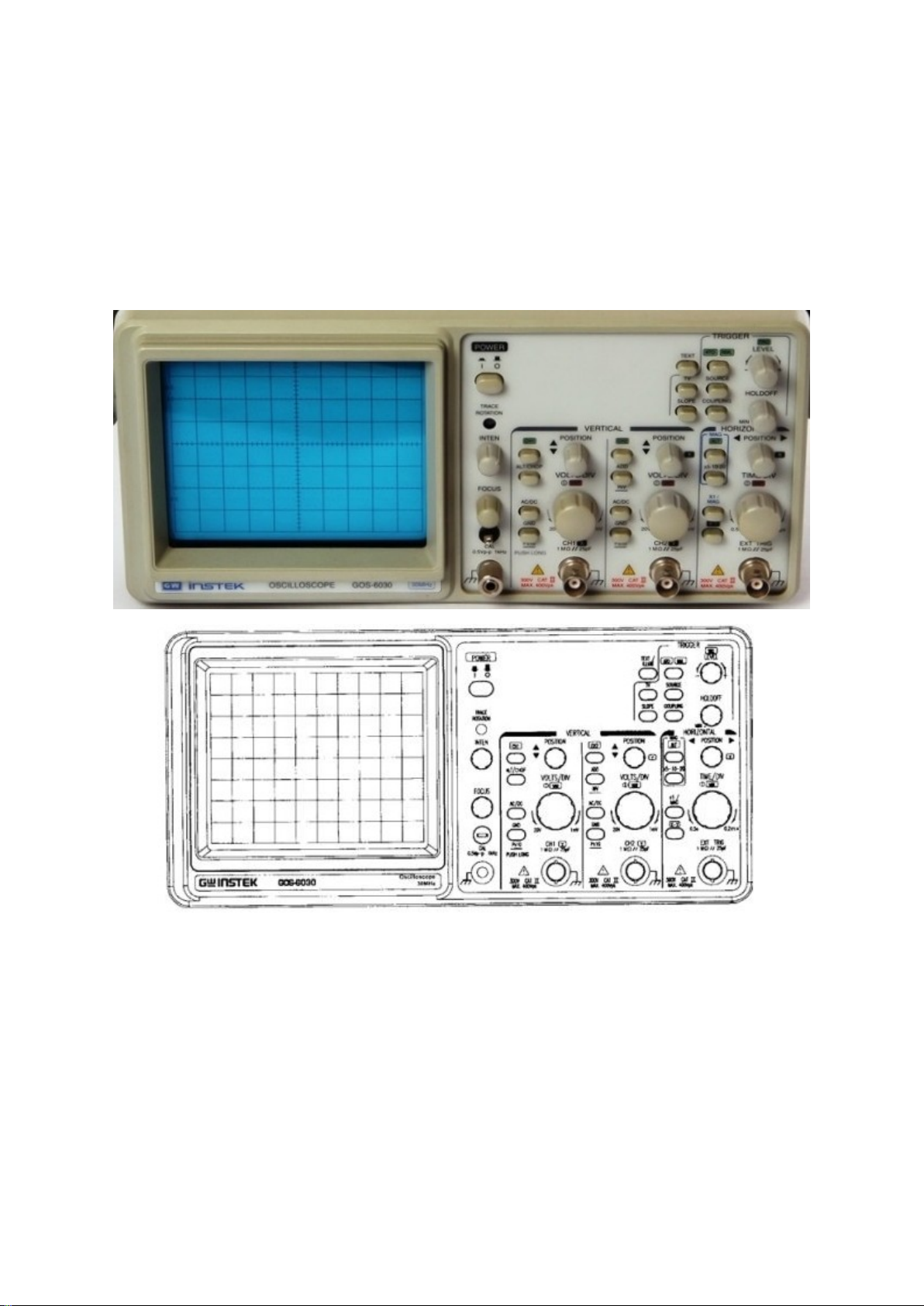
GW Instek GOS-6030 Oscilloscope
Schematics Only
Reverse Engineered from the PCB's
THIS IS NOT AN OFFICIAL DOCUMENT PLEASE USE WITH CAUTION
Bob Ford 2017 Rev 5
Page 2

GW Instek GOS-6030 Reverse Engineered Service Manual
Introduction
A few years ago the opportunity came along to purchase a number of GW-Instek GOS-6000 series
oscilloscopes, all with faults/damage. A deal was then agreed, and for better or worse I became the
owner of 16 6XXX oscilloscopes of varying specifications.
The collection was then stored in my shed for a number of months until time/weather/incentive all
peaked. The first step, find a set of manuals. Therein lay the first problem, as it would seem that
service information for all GW equipment is as rare as the proverbial RHS. Further investigation
confirmed that the manufacturer only supplies service documentation to dealers, or selected
service agents. Not good at all. After sending a few emails using the GW online enquiry service, with
no reply, the full horror of the situation dawned upon me, the scopes would need fixing without
reference to service documentation. Subsequent attempts to obtain spare parts also failed dismally.
It seems that ALL repairs should be through authorised dealers, and long gone are the days where
test equipment came with a full service manual from new, along with easy access to spares.
To cut a long story short, after fixing a couple of the scopes, and sketching out a number of partial
schematics as I traced each fault, I decided to combine all of the schematic portions into a proper
circuit diagram for much of the entire scope. At present it focusses on the 6030, however the other
models with higher bandwidth use essentially the same circuits, but with small changes in
transistor, CRT, and various component value changes. At some point I hope to group all variations
in this document.
In the end this took about 3 months of spare time, on and off to complete whilst still looking into
other faults. The end result comprises this document. The schematics are a mixture of sections
drawn from scratch, and others edited by cut and paste in ‘Paint’, from other oscilloscope
schematics. Because the circuit diagrams have evolved over time, they do not ‘flow’ in a logical way.
They are what they are, a group of interconnected blocks, which can make them tricky to
understand when deciding what the circuits are doing. The limited amount of on-line service
information for GW products was used as a basis for the ‘cut and paste’ stuff, as some circuitry from
the GOS- 600, GOS-61XX and GOS-62XX series ‘scopes is similar in a lot of cases. There are also
strong similarities to some Isotech and Tenma circuits, plus I feel sure other re-branded ‘scopes will
show a common parentage. Should anyone find errors, or have additional scraps of circuits from
this or other GW ‘scopes, please leave details on this forum.
I must stress that this is still work in progress, is far from complete, and most likely contains errors.
So please use with the above limitations in mind.
In the end, I hope it is better than nothing!
Page 3

Block Diagram
Applicable GOS-6030 PCB Assemblies
Page 4

OS-10P04C-2 CPU Board
OS-10P01C Input Amp Board
OS-01P03G-4 CRT Board
OS-10P03G-1 HV PSU Board
OS-10P03F-1 HV PSU Board (Build 2)
OS-10P03G-5 LV PSU Board
OS-10P02D X Drive Board
OS-10P03G-6 Y Drive Board
? Front Panel Board
OS10P03G-03 Potentiometer Board
Page 5

Description
The GOS-6030 oscilloscope is the base model from a small range with varying bandwidths,
capabilities and features (6031, 6051 etc.), the third digit indicates the bandwidth in MHz, and the
last digit the specification level.
My guess is that most, if not all of the internal circuit boards are common across the range (which I
will confirm as I investigate the scopes in more depth), with a few extra boards installed, or varying
build levels on the common modules to extend the specifications. The 6030 has 9 separate PCB’s,
with a mixture of PTH and SM build styles, the SM being double sided, and the PTH single sided. The
single sided boards, especially the ‘X’ drive board, come with a vast array of ‘link’ wires. These links
made/make fault finding on the ‘X’ board (to me) particularly difficult. Unfortunately the majority of
faults that I encountered were on this board, and I did come to loath it’s ‘patchwork quilt’ design, as
when tracing the circuit very few tracks go straight from one component to another. My guess is
that the board is a result of integrating older designs from individual boards onto a single one. This
may also be borne out by the odd range of component numbers on the board, R5XX, R8XX, R2XXX
etc.
The design changes means the 6XXX use momentary controls (digital), this being the main
difference from the 6XX series, which used conventional mechanical switches.
Page 6

Fault/Servicing Notes
• Be careful of sharp edges on the chassis. It will bite!
• With any brightness issues or dim/weak traces, first check the CRT board for dry joints
• Access to the X input circuits can be tricky. Desoldering the screening plate at the two rear
corners, and then sliding the plate to the rear will give access to the components. Undo the
6 fixing screws through holes in the PCB will allow the complete panel to be removed by
sliding backwards and tilting upwards, be careful though as the front of the panel will jam
against the boss on the plastic foot
• The ‘X’ I/P circuits are roughly the same as the GWInstek GOS6200 ‘scopes. Until I get
around to mapping the I/P board schematic, it will do at a pinch for general signal flow
• Main problems seem to be with the PSU’s. The HV unit seems to eat the HT diode D1012.
I’ve used R3000 ones as a substitute. Dry joints around the HV transformer are another
issue.
• The LV PSU has a bunch of regulators and transistors that are fixed to the chassis for heat
sink purposes, however I have rebuilt a board with the heatsinks and regulators etc. fitted to
the PCB. During use the heat sinks do not get overly hot, so maybe it’s only really needed on
the scopes with more boards/features where more current is drawn
• The mains switch is a very weak area, I have found 3 scopes, all in new physical condition
with O/C switches. I have been unable to find an exact replacement, but there are many
versions available that can be used with a small amount of PCB fettling. This is another of my
gripes about these scopes. The mains switch is fitted to the LV PSU PCB, and makes removal
of the board a bit of a faff. I’m looking at alternate ways to mount the switch in future, and
remove it from the PCB completely
• The relays on the X I/P board are all A5W-K, 2 Pole 2 Pos. Pin1 is at the black line marking,
and not the square indentation in the plastic case
• Most of the S/M component on the X I/P board lack identification markings. This makes it
tricky to transfer to a schematic
Page 7
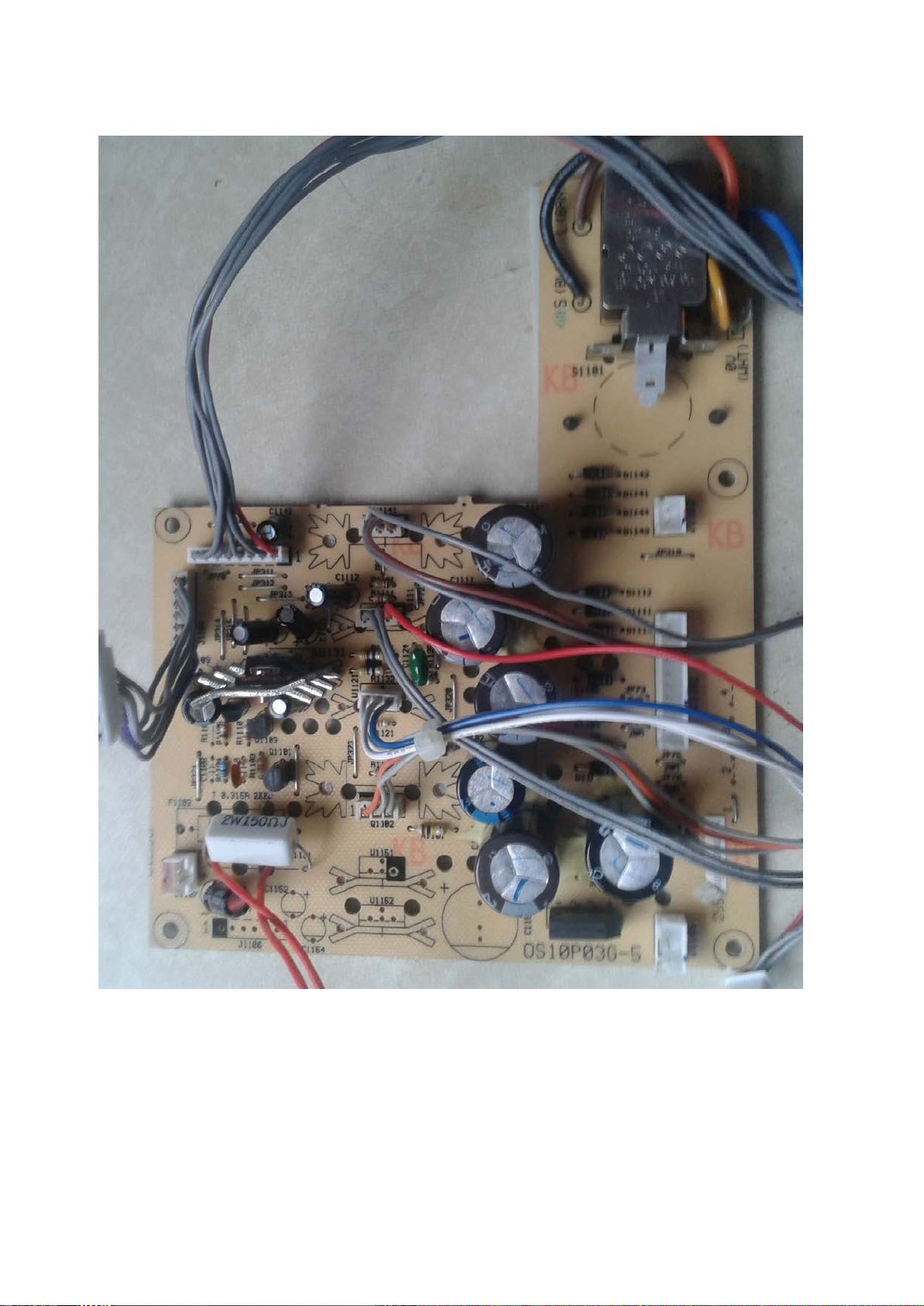
LV Power Supply Board Image
Page 8

LV Power Supply Board Schematic
Page 9

HV Power Supply Board Image
Page 10

HV Power Supply Board Image (Type 2)
Page 11

HV Power Supply Board Schematic
Page 12

CRT Board Schematic
Page 13

Potentiometer Board Schematic
Page 14

X Board Image
Page 15

X Board Schematics
Page 16

X Board Schematics
Page 17

X Board Schematics
Page 18

Y Board Image
Page 19

Y Board Schematic
Page 20

X Pre Amp Board
Page 21

CPU Board
 Loading...