


General Semiconductor 1N4717, 1N4716, 1N4715, 1N4710, 1N4709 Datasheet
...
SYMBOL MIN. MAX. UNIT
Thermal Resistance R
ΘJA
– 300
(1)
°C/W
Junction to Ambient Air
Forward Voltage V
F
– 1.5 Volts
at IF= 100 mA
SYMBOL VALUE UNIT
Zener Current (see Table “Characteristics”)
Power Dissipation at TL= 75°C, 3/8” from case P
tot
500 mW
Maximum Junction Temperature T
j
175 °C
Storage Temperature Range T
S
– 65 to +175 °C
12/2/98
FEATURES
♦ Silicon Planar Zener Diodes
♦ Standard Zener voltage tolerance is ± 5%.
Other tolerances are available
upon request.
♦ High temperature soldering guaranteed:
250°C/10 seconds, 0.375” (9.5mm) lead length.
♦ These diodes are also available in SOD-123 case
with the type designation MMSZ4681...MMSZ4717
and SOT-23 case with the type designation
MMBZ4681...MMBZ4717.
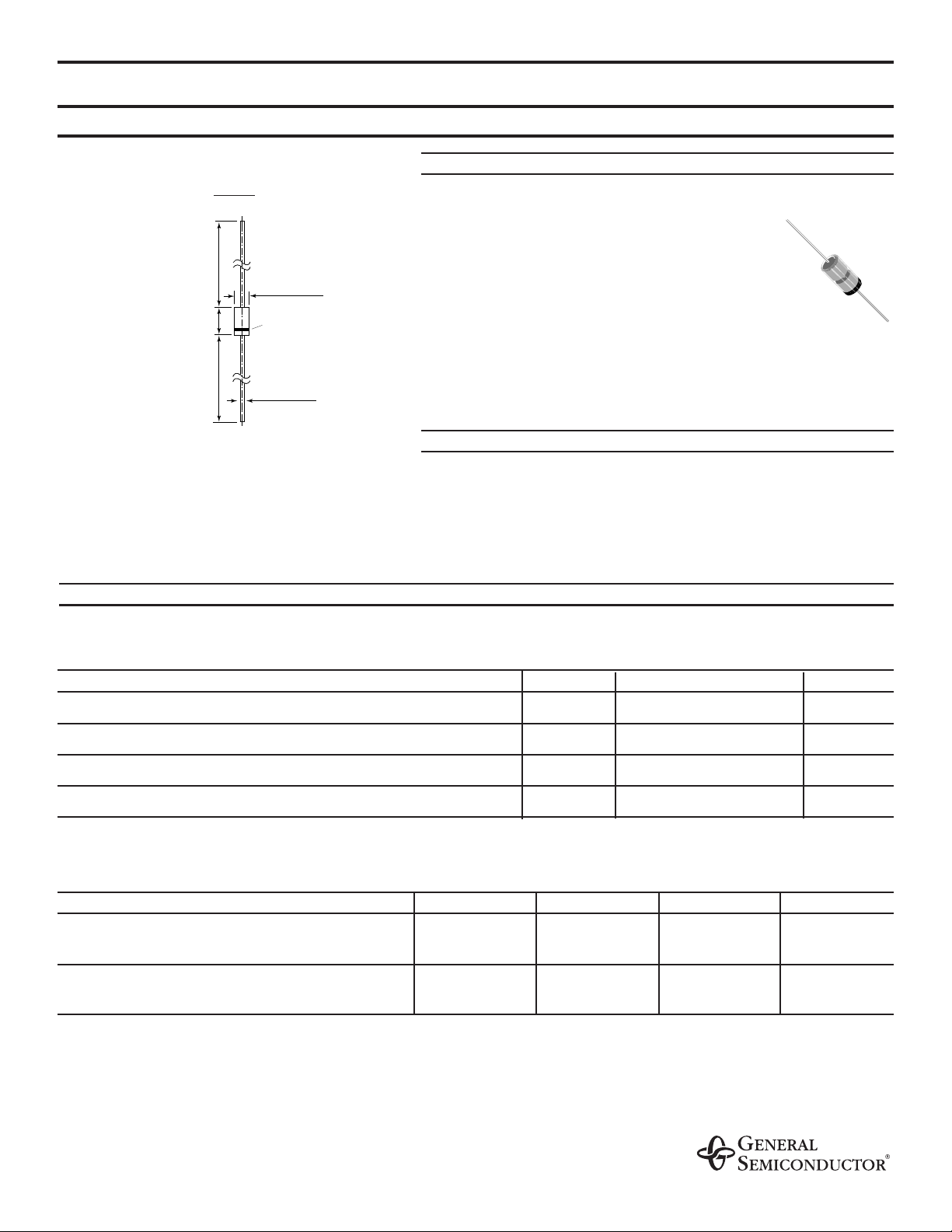
MECHANICAL DATA
Case: DO-35 Glass Case
Weight: approx. 0.13 g
Terminals: Solderable, per MIL-STD-750, method 2026.
MAXIMUM RATINGS
Ratings at 25°C ambient temperature unless otherwise specified.
1N4681 THRU 1N4717
ZENER DIODES
min. 1.083 (27.5)
min. 1.083 (27.5)
max. .150 (3.8)
max.
∅
Cathode
.020 (0.52)
Mark
max.
∅
.079 (2.0)
DO-35
Dimensions are in inches and (millimeters)
NOTES:
(1) Valid provided that leads at a distance of 3/8” mm from case are kept at ambient temperature.
ADVANCED INFORMATION

1N4681 THRU 1N4717
ELECTRICAL CHARACTERISTICS
Type
Zener Voltage
(1)
VZ @ lz= 50µA (Volts)
Max Reverse
Current I
R
(µA)
Max Zener
Current
I
ZM
(mA)
Test Voltage
V
R
(Volts)
Max Voltage Change
∆V
Z
(Volts)
(2)
1N4678 1.8 1.71 1.89 7.5 1.0 120 0.70
1N4679 2.0 1.90 2.10 5.0 1.0 110 0.70
1N4680 2.2 2.09 2.31 4.0 1.0 100 0.75
1N4681 2.4 2.28 2.52 2.0 1.0 95.0 0.80
1N4682 2.7 2.57 2.84 1.0 1.0 90.0 0.85
1N4683 3.0 2.85 3.15 0.8 1.0 85.0 0.90
1N4684 3.3 3.14 3.47 7.5 1.5 80.0 0.95
1N4685 3.6 3.42 3.78 7.5 2.0 75.0 0.95
1N4686 3.9 3.71 4.10 5.0 2.0 70.0 0.97
1N4687 4.3 4.09 4.52 4.0 2.0 65.0 0.99
1N4688 4.7 4.47 4.94 10.0 3.0 60.0 0.99
1N4689 5.1 4.85 5.36 10.0 3.0 55.0 0.97
1N4690 5.6 5.32 5.88 10.0 4.0 50.0 0.96
1N4691 6.2 5.89 6.51 10.0 5.0 45.0 0.95
1N4692 6.8 6.46 7.14 10.0 5.1 35.0 0.90
1N4693 7.5 7.13 7.88 10.0 5.7 31.8 0.75
1N4694 8.2 7.79 8.61 1.0 6.2 29.0 0.50
1N4695 8.7 8.27 9.14 1.0 6.6 27.4 0.10
1N4696 9.1 8.65 9.56 1.0 6.9 26.2 0.08
1N4697 10 9.50 10.5 1.0 7.6 24.8 0.10
1N4698 11 10.5 11.6 0.05 8.4 21.6 0.11
1N4699 12 11.4 12.6 0.05 9.1 20.4 0.12
1N4700 13 12.4 13.7 0.05 9.8 19.0 0.13
1N4701 14 13.3 14.7 0.05 10.6 17.5 0.14
1N4702 15 14.3 15.8 0.05 11.4 16.3 0.15
1N4703 16 15.2 16.8 0.05 12.1 15.4 0.16
1N4704 17 16.2 17.9 0.05 12.9 14.5 0.17
1N4705 18 17.1 18.9 0.05 13.6 13.2 0.18
1N4706 19 18.1 20.0 0.05 14.4 12.5 0.19
1N4707 20 19.0 21.0 0.01 15.2 11.9 0.20
1N4708 22 20.9 23.1 0.01 16.7 10.8 0.22
1N4709 24 22.8 25.2 0.01 18.2 9.9 0.24
1N4710 25 23.8 26.3 0.01 19.0 9.5 0.25
1N4711 27 25.7 28.4 0.01 20.4 8.8 0.27
1N4712 28 26.6 29.4 0.01 21.2 8.5 0.28
1N4713 30 28.5 31.5 0.01 22.8 7.9 0.30
1N4714 33 31.4 34.7 0.01 25.0 7.2 0.33
1N4715 36 34.2 37.8 0.01 27.3 6.6 0.36
1N4716 39 37.1 41.0 0.01 29.6 6.1 0.39
1N4717 43 40.9 45.2 0.01 32.6 5.5 0.43
NOTES:
(1) Tested with pulses, t
p
= 5ms
(2) ∆V
Z
is the difference between VZat 100µA and at 10µA.
Nominal Min Max
(TA= 25°C, unless otherwise specified.)
 Loading...