

FEATURES
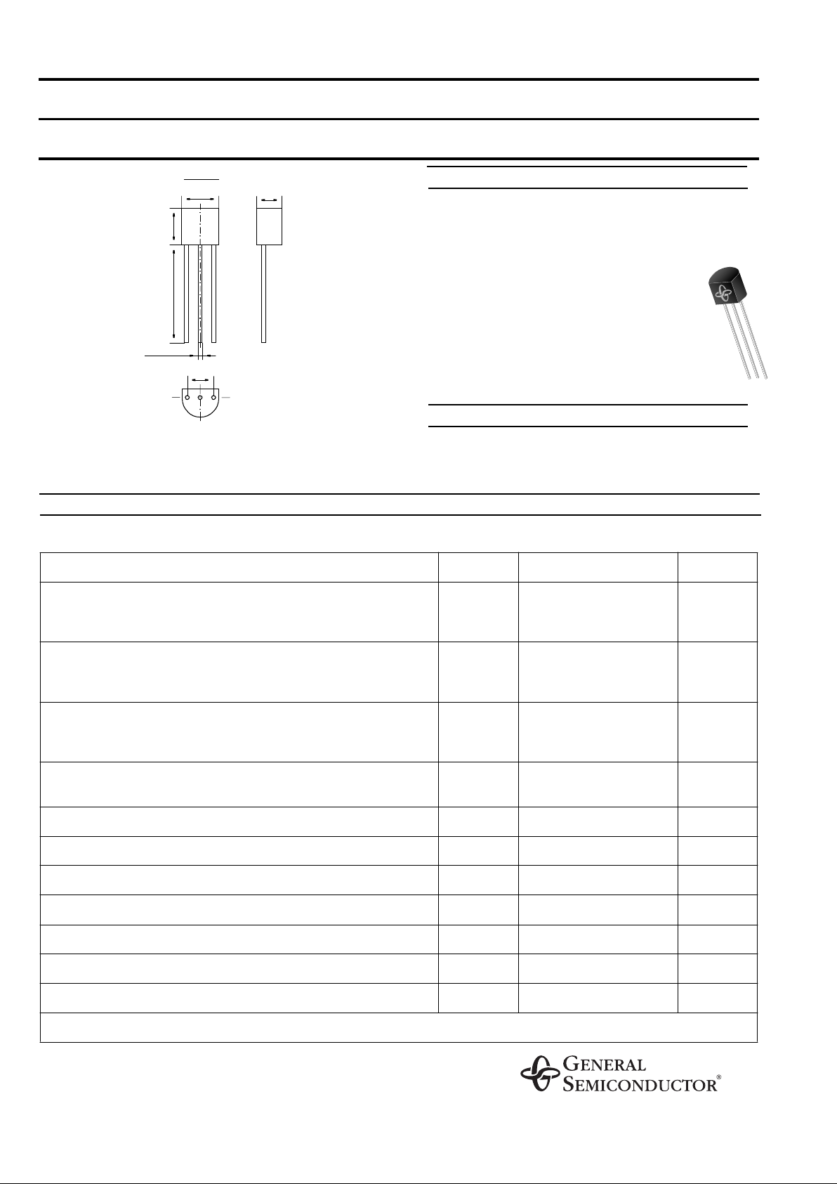
MECHANICAL DATA
Case:
TO-92 Plasti c Package
Weight:
approx. 0.18 g
MAXIMUM RATINGS AND ELECTRICAL CHARACTERISTICS
Small Signal Transistor s (NPN)
B
E
C
.181 (4.6)
min. .492 (12.5)
.181 (4.6)
.142 (3.6)
Dimensions in inches and (millimeters)
TO-92
Ratings at
25 °C
ambient temperature unless otherwise specified
.098 (2.5)
max.
∅
.022 (0.55)
4/98
BC546 THRU BC549
Symbol Value Unit
Collector-Base V oltage BC546
BC547
BC548, BC549
V
CBO
V
CBO
V
CBO
80
50
30
V
V
V
Collector-Emitter Voltage BC546
BC547
BC548, BC549
V
CES
V
CES
V
CES
80
50
30
V
V
V
Collector-Emitter Voltage BC546
BC547
BC548, BC549
V
CEO
V
CEO
V
CEO
65
45
30
V
V
V
Emitter-Base Voltage BC546, BC547
BC548, BC549
V
EBO
V
EBO
6
5
V
V
Collector Current I
C
100 mA
Peak Collector Current I
CM
200 mA
Peak Base Current I
BM
200 mA
Peak Emitter Current –I
EM
200 mA
Power Dissipation at T
amb
= 25 °C P
tot
500
1)
mW
Junction Temperature T
j
150 °C
Storage Temperature Range T
S
–65 to +150 °C
1)
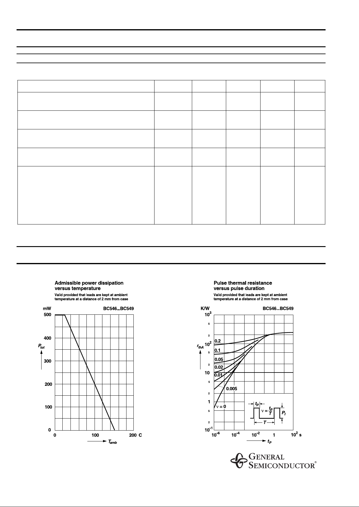
Valid provided that leads are kept at ambient temperature at a distance of 2 mm from case
NPN Silicon Epitaxial Planar Transistors
These transistors are subdivided into three groups
A, B and C according to their current gain. The type
BC546 is available in groups A and B, however, the types BC547 and BC548 can be
supplied in all three groups. The BC549 is a
low-noise type and available in groups B and
C. As complementary types, the PNP transistors BC556 … BC559 are recommended.
On special request, these transistors are also
manufactured in the pin configuration TO-18.
♦
♦
♦

ELECTRICAL CHARACTERISTICS
Ratings at
25 °C
ambient temperature unless otherwise specified
Symbol Min. Typ. Max. Unit
h-Parameters at VCE = 5 V, IC = 2 mA,
f = 1 kHz,
Small Signal Current Gain
Current Gain Group A
B
C
Input Impedance
Current Gain Group A
B
C
Output Admittance
Current Gain Group A
B
C
Reverse Voltage Transfer Ratio
Current Gain Group A
B
C
h
fe
h
fe
h
fe
h
ie
h
ie
h
ie
h
oe
h
oe
h
oe
h
re
h
re
h
re
–
–
–
1.6
3.2
6
–
–
–
–
–
–
220
330
600
2.7
4.5
8.7
18
30
60
1.5 · 10
–4
2 · 10
–4
3 · 10
–4
–
–
–
4.5
8.5
15
30
60
110
–
–
–
–
–
–
k
Ω
k
Ω
k
Ω
µ
S
µ
S
µ
S
–
–
–
DC Current Gain
at V
CE
= 5 V, IC = 10µA
Current Gain Group A
B
C
at VCE = 5 V, IC = 2 mA
Current Gain Group A
B
C
at VCE = 5 V, IC = 100 mA
Current Gain Group A
B
C
h
FE
h
FE
h
FE
h
FE
h
FE
h
FE
h
FE
h
FE
h
FE
–
–
–
110
200
420
–
–
–
90
150
270
180
290
500
120
200
400
–
–
–
220
450
800
–
–
–
–
–
–
–
–
–
–
–
–
Thermal Resistance Junction to Ambient Air R
thJA
– – 250
1)
K/W
Collector Saturation Voltage
at I
C
= 10 mA, IB = 0.5 mA
at I
C
= 100 mA, IB = 5 mA
V
CEsat
V
CEsat
–
–
80
200
200
600
mV
mV
Base Saturation Voltage
at I
C
= 10 mA, IB = 0.5 mA
at I
C
= 100 mA, IB = 5 mA
V
BEsat
V
BEsat
–
–
700
900
–
–
mV
mV
Base-Emitter Voltage
at V
CE
= 5 V, IC = 2 mA
at V
CE
= 5 V, IC = 10 mA
V
BE
V
BE
580
–
660
–
700
720
mV
mV
Collector-Emitter Cutoff Current
at V
CE
= 80 V BC546
at V
CE
= 50 V BC547
at V
CE
= 30 V BC548, BC549
at V
CE
= 80 V, Tj = 125 °C BC546
at V
CE
= 50 V, Tj = 125 °C BC547
I
CES
I
CES
I
CES
I
CES
I
CES
–
–
–
–
–
0.2
0.2
0.2
–
–
15
15
15
4
4
nA
nA
nA
µ
A
µ
A
1)
Valid provided that leads are kept at ambient temperature at a distance of 2 mm from case
BC546 THRU BC549
ELECTRICAL CHARACTERISTICS
Ratings at
25 °C
ambient temperature unless otherwise specified
Symbol Min. Typ. Max. Unit
at V
CE
= 30 V, Tj = 125 °C BC548, BC549 I
CES
––4
4
µ
A
µ
A
Gain-Bandwidth Product
at V
CE
= 5 V, IC = 10 mA, f = 100 MHz
f
T
– 300 – MHz
Collector-Base Capac itance
at V
CB
= 10 V, f = 1 MHz
C
CBO
–3.56pF
Emitter-Base Capacitance
at V
EB
= 0.5 V, f = 1 MHz
C
EBO
–9–pF
Noise Figure
at V
CE
= 5 V, IC = 200 µA, RG = 2 kΩ,
f = 1 kHz, ∆f = 200 Hz BC546, BC547
BC548
BC549
at V
CE
= 5 V, IC = 200 µA, RG = 2 kΩ,
f = 30…15000 Hz BC549
F
F
F
–
–
–
2
1.2
1.4
10
4
4
dB
dB
dB
BC546 THRU BC549
RATINGS AND CHARACTERISTIC CURVES BC546 THRU BC549

RATINGS AND CHARACTERISTIC CURVES BC546 THRU BC549

RATINGS AND CHARACTERISTIC CURVES BC546 THRU BC549

RATINGS AND CHARACTERISTIC CURVES BC546 THRU BC549
 Loading...