

Page 1
Data Sheet
October 5, 2009
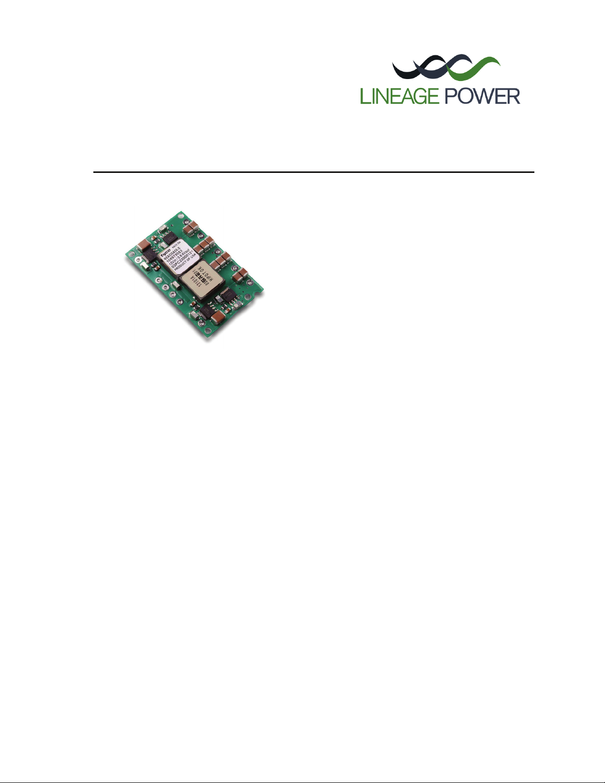
NaOSTM NXA025 SMT Non-isolated Power Modules:
10Vdc – 14Vdc Input; 0.8Vdc to 5.5Vdc Output; 25A Output Current
RoHS Compliant
Applications
Distributed power architectures
Intermediate bus voltage applications
Telecommunications equipment
Servers and storage applications
Networking equipment
Enterprise Networks
Latest generation IC’s (DSP, FPGA, ASIC)
and Microprocessor powered applications
Options
Baseplate version for heatsink attachment
(-H suffix)
Through Hole version (-L)
Paralleling with current sharing (-P)
Features
Compliant to RoHS EU Directive 2002/95/EC (-Z
versions)
Compliant to ROHS EU Directive 2002/95/EC with
lead solder exemption (non-Z versions)
Delivers up to 25A output current
High efficiency – 93% at 3.3V full load
Small size and low profile:
47.2 mm x 29.4 mm x 8.50 mm
(1.86 in x 1.16 in x 0.335 in)
Low output ripple and noise
Constant switching frequency (500 kHz)
Surface mount or through hole
Output voltage programmable from 0.8 Vdc to
5.5Vdc via external resistor
Remote On/Off
Remote Sense
Parallel operation with current sharing (-P option)
Output voltage sequencing (multiple modules)
Output overvoltage protection
Overtemperature protection
Output overcurrent protection (non-latching)
Wide operating temperature range (-40°C to 85°C)
†
UL* 60950-1Recognized, CSA
03 Certified, and VDE
Licensed
ISO** 9001 and ISO 14001 certified manufacturing
facilities
‡
0805:2001-12 (EN60950-1)
C22.2 No. 60950-1-
Description
The NXA025 series SMT (surface-mount technology) power modules are non-isolated dc-dc converters that can
deliver up to 25A of output current with full load efficiency of 93% at 3.3Vdc output voltage. These modules provide
a precisely regulated output voltage from 0.8Vdc to 5.5Vdc, programmable via an external resistor. Their openframe construction and small footprint enable designers to develop cost- and space-efficient solutions. Standard
features include remote On/Off, adjustable output voltage, remote sense, active current sharing between parallel
modules, output voltage sequencing of multiple modules, overcurrent, overvoltage, and overtemperature protection.
* UL is a re gistered trademark of Underwriters Laboratories, Inc.
†
CSA is a reg istered trademark of Canadian Standards Associ ation.
‡
VDE is a t rademark of Verband Deutscher Elektrotechniker e.V.
** ISO is a registered trademark of the International Orga nization of Standards
Document No: DS03-030 ver. 1.43
PDF name: nxa025_smt_ds.pdf
Page 2
Data Sheet
October 5, 2009
10 – 14Vdc Input; 0.8Vdc to 5.5Vdc Output; 25A output current
Naos
TM
NXA025 SMT Non-isolated Power Modules:
Absolute Maximum Ratings
Stresses in excess of the absolute maximum ratings can cause permanent damage to the device. These are
absolute stress ratings only, functional operation of the device is not implied at these or any other conditions in
excess of those given in the operations sections of the data sheet. Exposure to absolute maximum ratings for
extended periods can adversely affect the device reliability.
Parameter Device Symbol Min Max Unit
Input Voltage All V
Continuous
Operating Ambient Temperature All T
(see Thermal Considerations section)
Storage Temperature All T
IN
A
stg
-0.3 14 Vdc
-40 85 °C
-55 125 °C
Electrical Specifications
Unless otherwise indicated, specifications apply over all operating input voltage, resistive load, and temperature
conditions.
Parameter Device Symbol Min Typ Max Unit
Operating Input Voltage All VIN 10.0 12.0 14.0 Vdc
Maximum Input Current All I
(VIN=10.0V to 14.0V, IO=I
Inrush Transient All I2t 1 A2s
Input Reflected Ripple Current, peak-to-peak
(5Hz to 20MHz, 1μH source impedance; V
V
= I
IN, max, IO
Input Ripple Rejection (120Hz) All 50 dB
; See Test configuration section)
Omax
)
O, max
IN, min
to
All 60 mAp-p
IN,max
CAUTION: This power module is not internally fused. An input line fuse must always be used.
This power module can be used in a wide variety of applications, ranging from simple standalone operation to being
part of a complex power architecture. To preserve maximum flexibility, internal fusing is not included, however, to
achieve maximum safety and system protection, always use an input line fuse. The safety agencies require a fastacting fuse with a maximum rating of 30A (see Safety Considerations section). Based on the information provided in
this data sheet on inrush energy and maximum dc input current, the same type of fuse with a lower rating can be
used. Refer to the fuse manufacturer’s data sheet for further information.
14 Adc
LINEAGE POWER 2
Page 3

Data Sheet
October 5, 2009
10 – 14Vdc Input; 0.8Vdc to 5.5Vdc Output; 25A output current
Naos
TM
NXA025 SMT Non-isolated Power Modules:
Electrical Specifications (continued)
Parameter Device Symbol Min Typ Max Unit
Output Voltage Set-point All V
(VIN=V
N, min
, IO=I
, TA=25°C)
O, max
Output Voltage All V
(Over all operating input voltage, resistive load,
and temperature conditions until end of life)
Adjustment Range All V
Selected by an external resistor
O, set
O, set
O
Output Regulation
Line (VIN=V
Load (IO=I
Temperature (T
IN, min
O, min
to V
to I
ref=TA, min
) All
IN, max
) All
O, max
to T
) All ⎯ 0.5 1 % V
A, max
Output Ripple and Noise on nominal output
(VIN=V
IN, nom
and IO=I
O, min
to I
O, max
Cout = 2 * 0.47μF ceramic capacitors)
RMS (5Hz to 20MHz bandwidth) All
Peak-to-Peak (5Hz to 20MHz bandwidth) All
External Capacitance
ESR ≥ 1 mΩ All C
ESR ≥ 10 mΩ All C
Output Current All I
Output Current Limit Inception (Hiccup Mode ) All I
Output Short-Circuit Current All I
(VO≤250mV) ( Hiccup Mode )
Efficiency V
VIN= V
IO=I
, TA=25°C V
IN, nom
= V
O, max , VO
V
O,set
V
V
V
V
V
= 0.8Vdc η 79.0 %
O,set
= 1.2Vdc η 84.7 %
O, set
= 1.5Vdc η 87.3 %
O,set
= 1.8Vdc η 88.9 %
O,set
= 2.0Vdc η 89.7 %
O,set
= 2.5Vdc η 91.4 %
O,set
= 3.3Vdc η 93.1 %
O,set
= 5.5Vdc η 95.1 %
O,set
Switching Frequency All f
O, max
O, max
o
O, lim
O, s/c
sw
Dynamic Load Response
(dIo/dt=5A/μs; VIN = V
IN, nom
; TA=25°C)
Load Change from Io= 50% to 100% of
Io,max; No external output capacitors
All V
pk
Peak Deviation
Settling Time (Vo<10% peak deviation)
(dIo/dt=5A/μs; VIN = V
IN, nom
; TA=25°C)
Load Change from Io= 100% to 50%of Io,max:
No external output capacitors
All t
All V
s
pk
Peak Deviation
Settling Time (Vo<10% peak deviation)
All t
s
-1.2
-3.0
⎯
⎯
+1.2 % V
+3.0 % V
0.7887 5.5 Vdc
⎯
⎯
⎯
⎯
0.01 0.1 % V
0.1 0.2 % V
5 15 mV
15 50 mV
⎯ ⎯
⎯ ⎯
1000 μF
10,000 μF
0 25 Adc
⎯
⎯
125 150 % I
1
⎯
⎯
⎯
⎯
⎯
⎯
500
⎯
150 mV
25
⎯ μs
150 mV
25
⎯ μs
pk-pk
Adc
kHz
O, set
O, set
O, set
O, set
O, set
rms
o
LINEAGE POWER 3
Page 4
Data Sheet
October 5, 2009
10 – 14Vdc Input; 0.8Vdc to 5.5Vdc Output; 25A output current
Naos
TM
NXA025 SMT Non-isolated Power Modules:
General Specifications
Parameter Min Typ Max Unit
Calculated MTBF (IO=80% of I
Weight
, TA=25°C) 2,150,000 Hours
O, max
⎯
15.5 (0.55)
⎯
g (oz.)
Feature Specifications
Unless otherwise indicated, specifications apply over all operating input voltage, resistive load, and temperature
conditions. See Feature Descriptions for additional information.
Parameter Device Symbol Min Typ Max Unit
SEQ/ENA Signal Interface
(VIN=V
Signal referenced to GND)
Logic High (SEQ/ENA pin open – Module Off)
SEQ/ENA Current All I
SEQ/ENA Voltage: All V
Logic Low (Module ON)
SEQ/ENA Current: All I
SEQ/ENA Voltage: All V
Turn-On Delay and Rise Times All Tdelay ― 1 ― msec
(IO=I
Output voltage overshoot – Startup 0.1
IO=80% of I
Ouptut Overvoltage Protection (Latching) All 5.62 5.8 6.0 V
Input Undervoltage Lockout
Turn-on Threshold All
Turn-off Threshold All
Remote Sense Range ― ― 0.5 V
Overtemperature Protection
(See Thermal Consideration section)
Forced Load Share Accuracy All
Number of units in Parallel
to V
IN, min
to within ±1% of steady state)
O, max , Vo
O, max
; open collector or equivalent,
IN, max
; VIN = 12Vdc, TA = 25 oC
SEQ/ENA
SEQ/ENA
SEQ/ENA
SEQ/ENA
All Trise
All T
ref
0.5
3.5
⎯
⎯
2.33 mA
14 V
⎯ ⎯
⎯ ⎯
― 5 ― msec
200 μA
1.2 V
0.5
9.9 V
8.1 V
⎯
125
⎯
⎯
10 % Io
5
% V
°C
O, set
LINEAGE POWER 4
Page 5
Data Sheet
October 5, 2009
10 – 14Vdc Input; 0.8Vdc to 5.5Vdc Output; 25A output current
Naos
TM
NXA025 SMT Non-isolated Power Modules:
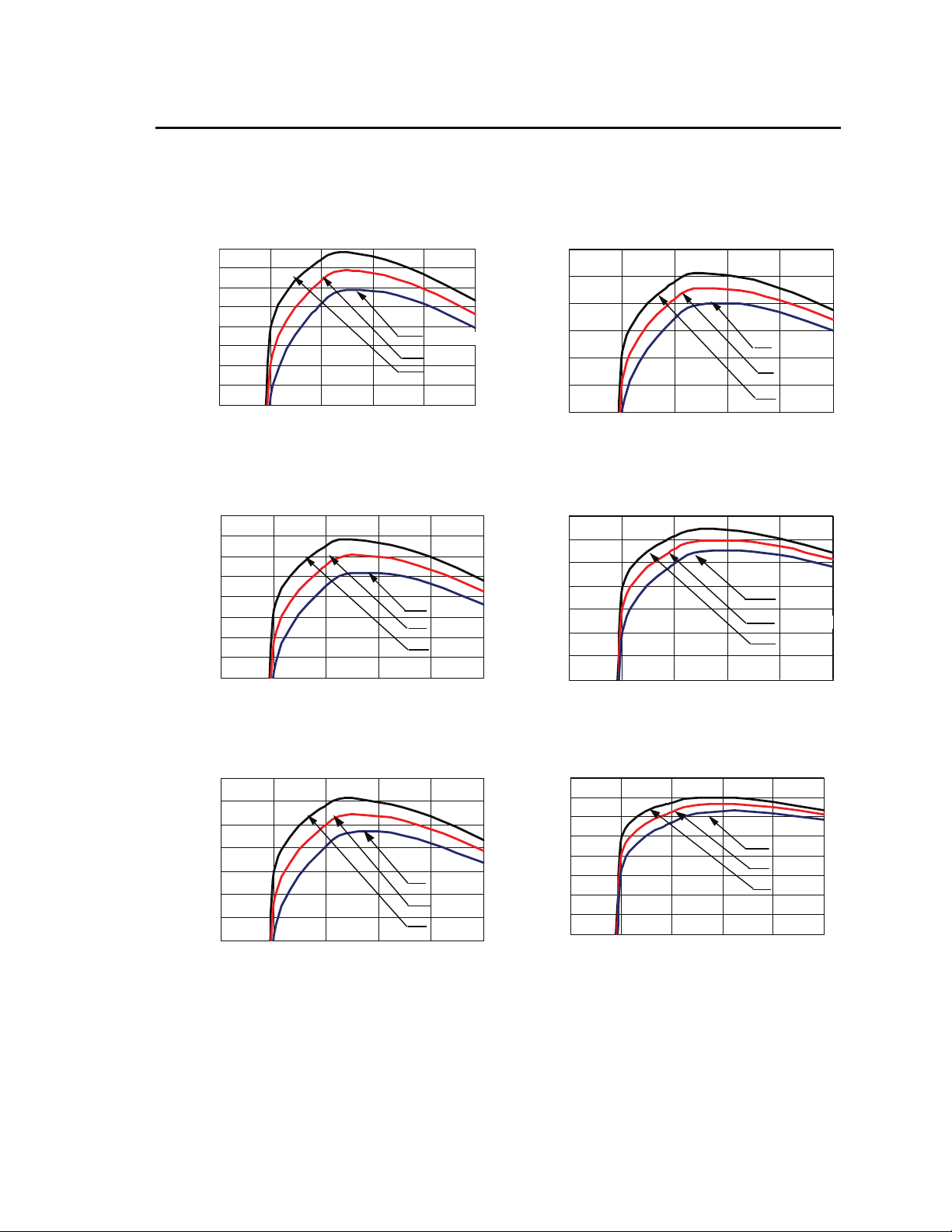
Characteristic Curves
The following figures provide typical characteristics for the NXA025A0X –S at 25ºC.
88%
87%
86%
85%
84%
83%
82%
81%
EFFICIENCY, η (%)
80%
0 5 10 15 2 0 2 5
Vin=13.2V
Vin=12.0V
Vin=10.8V
OUTPUT CURRENT, IO (A)
Figure 1. Converter Efficiency versus Output Current
(Vout = 1.2Vdc).
91%
90%
89%
88%
87%
86%
85%
84%
EFFICIENCY, η (%)
83%
Vin=13.2V
Vin=12.0V
Vin=10.8V
0 5 10 15 2 0 2 5
OUTPUT CURRENT, IO (A)
Figure 2. Converter Efficiency versus Output Current
(Vout = 1.5Vdc).
92%
91%
90%
89%
88%
87%
86%
EFFICIENCY, η (%)
85%
0 5 10 15 2 0 2 5
Vin=13.2V
Vin=12.0V
Vin=10.8V
94%
93%
92%
91%
90%
89%
EFFICIENCY, η (%)
88%
0 5 10 15 2 0 2 5
OUTPUT CURRENT, IO (A)
Figure 4. Converter Efficiency versus Output Current
(Vout = 2.5Vdc).
95%
94%
93%
92%
91%
90%
89%
EFFICIENCY, η (%)
88%
0 5 10 15 2 0 2 5
OUTPUT CURRENT, IO (A)
Figure 5. Converter Efficiency versus Output Current
(Vout = 3.3Vdc).
97%
96%
95%
94%
93%
92%
91%
90%
EFFICIENCY, η (%)
89%
0 5 10 15 2 0 2 5
Vin=13.2V
Vin=12.0V
Vin=10.8V
Vin=13.2V
Vin=12.0V
Vin=10.8V
Vin=13.2V
Vin=12.0V
Vin=10.8V
OUTPUT CURRENT, IO (A)
Figure 3. Converter Efficiency versus Output Current
(Vout = 1.8Vdc).
Figure 6. Converter Efficiency versus Output Current
(Vout = 5.0Vdc).
OUTPUT CURRENT, IO (A)
LINEAGE POWER 5
Page 6
Data Sheet
)
October 5, 2009
10 – 14Vdc Input; 0.8Vdc to 5.5Vdc Output; 25A output current
Naos
TM
NXA025 SMT Non-isolated Power Modules:
Characteristic Curves (continued)
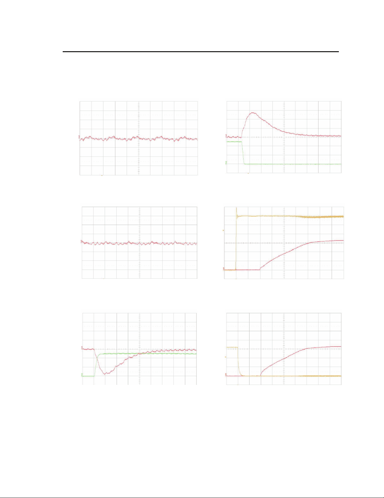
The following figures provide typical characteristics for the NXA025A0X –S at 25ºC.
(V) (20mV/div)
O
V
OUTPUT VOLTAGE
(V) (50mV/div)
O
Figure 7. Typical Output Ripple and Noise (Vin = 12V
TIME, t (1μs/div
dc, Vo = 3.3 Vdc, Cout = 2x 0.47uF ceramic capacitor).
(V) (20mV/div)
O
V
OUTPUT VOLTAGE
TIME, t (1μs/div)
Figure 8. Typical Output Ripple and Noise (Vin = 12V
dc, Vo = 1.2Vdc, Cout = 2x 0.47uF ceramic capacitor).
(V) (50mV/div)
O
(A) (5A/div) V
O
OUTPUT CURRENT, OUTPUT VOLTAGE
I
TIME, t (5 μs/div)
Figure 10. Transient Response to Dynamic Load
Change from 100% to 50% of full load (Vo = 3.3Vdc).
(V) (2V/div)
IN
(V) (1V/div) V
o
OUTPUT VOLTAGE, INPUT VOLTAGE
V
TIME, t (0.5ms/div)
Figure 11. Typical Start-Up with application of Vin (Vo
= 3.3Vdc).
(V) (2V/div)
On/off
(A) (5A/div) V
O
I
OUTPUT CURRENT OUTPUT VOLTAGE
TIME, t (5μs/div)
Figure 9. Transient Response to Dynamic Load
Change from 50% to 100% of full load (Vo = 3.3Vdc).
V) (1V/div) V
O
OUTPUT VOLTAGE On/Off VOLTAGE
V
TIME, t (0.5ms/div)
Figure 12. Typical Start-Up Using Enable (Vo =
3.3Vdc).
LINEAGE POWER 6
Page 7
Data Sheet
,
October 5, 2009
10 – 14Vdc Input; 0.8Vdc to 5.5Vdc Output; 25A output current
Naos
TM
NXA025 SMT Non-isolated Power Modules:
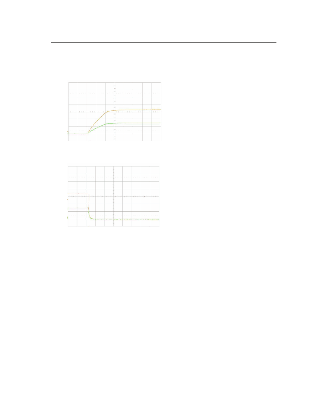
Characteristic Curves (continued)
The following figures provide typical characteristics for the NXA025A0X –S at 25oC.
(V) (1V/div)
O
(V) (1V/div) V
O
Module # 1 Module #2
V
Figure 13. Synchronized Start-up of Output Voltage
when SEQ/ENA pins are tied together (Module #1 =
1.5Vdc
Module #2 = 3.3Vdc).
TIME, t (1ms/div)
(V) (1V/div)
O
(V) (1V/div) V
O
V
Module # 1 Module #2
TIME, t (1ms/div)
Figure 14. Synchronized Shut-down of Output Voltage
when SEQ/ENA pins are tied together (Module #1 =
1.5Vdc, Module #2 = 3.3Vdc).
LINEAGE POWER 7
Page 8

Data Sheet
October 5, 2009
10 – 14Vdc Input; 0.8Vdc to 5.5Vdc Output; 25A output current
Naos
TM
NXA025 SMT Non-isolated Power Modules:
Characteristic Curves (continued)
The following figures provide typical thermal derating curves for NXA025A0X –S (Figures 19 and 20 show derating
curves with base plate).
30
25
20
15
10
5
0
20 30 40 50 60 70 80
OUTPUT CURRENT, Io (A)
1
00LFM
200LFM
300LFM
400LFM
AMBIENT TEMPERATURE, TA OC
Figure 15. Derating Output Current versus Local
Ambient Temperature and Airflow (Vin = 12Vdc,
Vo=1.2Vdc).
OUTPUT CURRENT, Io (A)
30
25
20
15
10
5
0
20 30 40 50 60 70 80
00LFM
1
200LFM
300LFM
400LFM
AMBIENT TEMPERATURE, TA OC
Figure 16. Derating Output Current versus Local
Ambient Temperature and Airflow (Vin = 12Vdc,
Vo=1.8 Vdc).
30
25
1
20
15
10
5
0
20 30 40 50 60 70 80
OUTPUT CURRENT, Io (A)
00LFM
200LFM
300LFM
400LFM
AMBIENT TEMPERATURE, TA OC
Figure 17. Derating Output Current versus Local
Ambient Temperature and Airflow
(Vin = 12Vdc,
Vo=3.3 Vdc).
Figure 18. Derating Output Current versus Local
Ambient Temperature and Airflow (Vin = 12Vdc,
Vo=5.0 Vdc).
Figure 19. Derating Output Current versus Local
Ambient Temperature and Airflow (Vin = 12Vdc,
Vo=3.3 Vdc) with baseplate.
Figure 20. Derating Output Current versus Local
Ambient Temperature and Airflow (Vin = 12Vdc,
Vo=5.0 Vdc) with baseplate.
30
25
20
15
10
5
0
20 30 40 50 60 70 80
OUTPUT CURRENT, Io (A)
100LFM
200LFM
300LFM
400LFM
AMBIENT TEMPERATURE, TA OC
30
25
20
15
10
5
0
OUTPUT CURRENT, Io (A)
20 30 40 50 60 70 80
100 LFM
200 LFM
AMBIENT TEMPERATURE, TA OC
30
25
20
15
10
5
0
OUTPUT CURRENT, Io (A)
20 30 40 50 60 70 80
100 LFM
200 LFM
300 LFM
400 LFM
AMBIENT TEMPERATURE, TA OC
LINEAGE POWER 8
Page 9

Data Sheet
October 5, 2009
10 – 14Vdc Input; 0.8Vdc to 5.5Vdc Output; 25A output current
Naos
Test Configurations
COM
V
O
V
CURRENT PROBE
CIN
Min
150μF
SCOPE
R
contactRdistribution
O
R
contactRdistribution
x 100 %
VIN(+)
COM
RESISTIVE
LOAD
R
LOAD
TO OSCILLOSCOPE
L
TEST
1μH
CS 220μF
BATTERY
NOTE: Measure input reflected ripple current with a simulated
E.S.R.<0.1Ω
@ 20°C 100kHz
source indu ctance (L
possibl e batter y impedance. M easure cur rent as shown
above.
) of 1μH. Capacitor CS offsets
TEST
Figure 21. Input Reflected Ripple Current Test Setup.
COPPER STRIP
V
(+)
O
1uF .
COM
NOTE: All voltage measurements to be take n at the module
terminals, as shown above. If sockets are used then
Kelvin connections are required at the module terminals
to avoid measurement errors due to socket contact
resistance.
10uF
GROUND PLANE
Figure 22. Output Ripple and Noise Test Setup.
R
R
contact
distribution
R
R
contact
distribution
NOTE: All volt age meas urements to be taken at th e module
terminals , as shown above. If sock ets are us ed then
Kelvin c onnections are required at t he module termi nals
to avoid measur ement err ors due to soc ket contact
resistance.
VIN(+)
V
IN
COM
Figure 23. Output Voltage and Efficiency Test Setup.
. I
V
O
Efficiency
=
η
VIN. I
O
IN
TM
NXA025 SMT Non-isolated Power Modules:
Typical Application Circuit
C
IN
Share
Rtrim
Share
SEN+
SEQ/ENA
SEN-
4.99k
Rx
Dx
Qx
1uF
Figure 24. Application Schematic
Vin Vin
GND
GND
VIN
Vout
Vout
GND
Vout
Cout
Design Considerations
Input Source Impedance
The power module should be connected to a
low-impedance source. Highly inductive source
impedance can affect the stability of the power module.
The input capacitor C
from the two input pins of the module. C
recommended to be 150μF minimum. The ripple voltage
is 50mV RMS at 1MHz and the capacitor should be
chosen with an ESR and an RMS Current Rating for this
amount of ripple voltage. When using multiple modules
in parallel, a small inductor (0.2 –0.5μH) is recommended
at the input of each module to prevent interaction
between modules. Consult the factory for further
application guidelines.
IN should be located equal distance
IN is
Safety Considerations
For safety agency approval the power module must be
installed in compliance with the spacing and separation
requirements of the end-use safety agency standards,
i.e., UL 60950-1, CSA C22.2 No. 60950-1-03, and VDE
0850:2001-12 (EN60950-1) Licensed.
For the converter output to be considered meeting the
requirements of safety extra-low voltage (SELV), the
input must meet SELV requirements. The power module
has extra-low voltage (ELV) outputs when all inputs are
ELV.
The input to these units is to be provided with a maximum
of 30 A fast-acting fuse in the ungrounded lead.
LINEAGE POWER 9
Page 10

Data Sheet
k
October 5, 2009
TM
Naos
10 – 14Vdc Input; 0.8Vdc to 5.5Vdc Output; 25A output current
NXA025 SMT Non-isolated Power Modules:
Feature Description
Remote On/Off using SEQ/ENA Pin
The NXA025A0X-S SMT power modules feature an
SEQ/ENA pin for remote On/Off operation. If not using
the remote On/Off pin, leave the pin open (module will be
on). The SEQ/ENA signal (V
ground. Circuit configuration for remote On/Off operation
of the module using SEQ/ENA pin is shown in Figure 25.
During Logic High on the SEQ/ENA pin (transistor Qx is
OFF), the module remains OFF. The external resistor
Rx should be chosen to maintain 3.5V minimum on the
SEQ/ENA pin to insure that the unit is OFF when
transistor Qx is in the OFF state. During Logic-Low
when Qx is turned ON, the module is turned ON. Note
that the external diode is required to make sure the
internal thermal shutdown (THERMAl_SD) and
undervoltage (UVLO) circuits are not disabled when Qx is
turned ON
VIN
Rx
4.99k
SEQ/ENA
Pin
Dx
Qx
Figure 25. Remote On/Off Implementation.
The SEQ/ENA pin can also be used to synchronize the
output voltage start-up and shutdown of multiple modules
in parallel. By connecting SEQ/ENA pins of multiple
modules, the output start-up can be synchronized (please
refer to characterization curves). When SEQ/ENA pins
are connected together, all modules will shutdown if any
one of the modules gets disabled due to undervoltage
lockout or overtemperature protection.
Remote Sense
Remote sense feature minimizes the effects of
distribution losses by regulating the voltage at the remote
sense pins. The voltage between the remote sense pins
and the output terminals must not exceed the remote
sense range given in the Feature Specification table, i.e.:
[Vo
(+) – Vo(GND)] –[SENSE(+) – SENSE(-)] < 0.5V
Remote sense configuration is shown in Figure 26. If not
using the remote sense feature to regulate the output
SEQ/ENA) is referenced to
THERMAL_SD
UVLO
Enable
R
1
1
R
2
4.99k
voltage at the point of load, connect SENSE (+) to Vo(+)
and Sense (-) to ground. The amount of power delivered
by the module is defined as the voltage at the output
terminals multiplied by the output current. When using
the remote sense, the output voltage of the module can
be increased, which at the same output current would
increase the power output of the module. Ensure that the
maximum output power of the module remains at or
below the maximum rated power (Po,max = Io,max x
Vo,max).
Figure 26. Effective Circuit Configuration for Remote
sense operation
Overcurrent Protection
To provide protection in a fault (output overload)
condition, the unit is equipped with internal
current-limiting circuitry and can endure current limiting
continuously. At the point of current-limit inception, the
unit enters hiccup mode. The unit operates normally once
the output current is brought back into its specified range.
The average output current during hiccup is 10% I
Input Undervoltage Lockout
At input voltages below the input undervoltage lockout
limit, module operation is disabled. The module will begin
to operate at an input voltage above the undervoltage
lockout turn-on threshold.
Overtemperature Protection
To provide protection in a fault condition, the unit is
equipped with a thermal shutdown circuit. The unit will
shutdown if the thermal reference point T
o
125
C (typical), but the thermal shutdown is not
, exceeds
ref
intended as a guarantee that the unit will survive
temperatures beyond its rating. The module will
automatically restarts after it cools down.
Output Voltage Programming
The output voltage of the NXA025A0X-S can be
programmed to any voltage from 0.8Vdc to 5.5Vdc by
inserting a series resistor (shown as Rtrim in figure 27) in
the Sense(+) pin of the module. Without an external
resistor in the Sense
Vo
(+)), the output voltage of the module will be 0.7887V.
With Sense
(+) not connected to Vo(+), the output of the
module will reach overvoltage shutdown. A 1μF multilayer ceramic capacitor is required from Rtrim to Sense
pin to minimize noise. To calculate the value of the
(+) pin (Sense (+) pin is shorted to
O, max
.
(-)
LINEAGE POWER 10
Page 11

Data Sheet
October 5, 2009
10 – 14Vdc Input; 0.8Vdc to 5.5Vdc Output; 25A output current
Naos
Feature Descriptions (continued)
Output Voltage Programming (continued)
resistor Rtrim for a particular desired voltage Vo, use the
following equation:
Vo
⎡
Rtrim
*775
⎢
7887.0
⎣
Where Vo is the desired output voltage
and Rtrim is the external resistor in ohms
For example, to program the output voltage of the
NXA025A0X-S module to 2.5Vdc, Rtrim is calculated as
follows:
⎡
*775Rtrim
⎢
⎣
VIN(+)
ENA
V
Sense+
Share
O
R
7887.0
trim
1µF
⎤
Ω
−= 1
⎥
⎦
5.2
⎤
−= 1
⎥
⎦
Ω= 1682Rtrim
R
LOAD
TM
NXA025 SMT Non-isolated Power Modules:
Forced Load sharing (Parallel Operation)
For additional power requirements, the power module can
be configured for parallel operation with forced load
sharing (See Figure 28). Good layout techniques should
be observed for noise immunity when using multiple units
in parallel. To implement forced load sharing, the
following connections should be made:
• The share pins of all units in parallel must be
connected together. The path of these connections
should be as direct as possible.
• All remote-sense pins should be connected to the
power bus at the same point, i.e., connect all the
SENSE
(+) pins to the (+) side of the bus and all the
SENSE
(-) pins to the GROUND of the power bus at
the same point. Close proximity and directness are
necessary for good noise immunity
The share bus is not designed for redundant operation
and the system will be non-functional upon failure of one
of the unit when multiple units are in parallel. The
maximum number of modules tied to share bus is 5.
When not using the parallel feature, leave the share pin
open.
Sense-
COM
COM
Figure 27. Circuit Configuration for Programming
Output voltage
Table 1 provides Rtrim values required for most common
output voltages. To achieve the output voltage tolerance
as specified in the electrical specifications over all
operating input voltage, resistive load and temperature
conditions, use 0.1% thick metal film resistor.
Table 1
Vo,set
(V)
0.8 11
1.0 208
1.2 404
1.5 699
1.8 994
2.0 1190
2.5 1682
3.3 2468
5.0 4138
Overvoltage Shutdown Open
Rtrim
Ω
Figure 28. Circuit Configuration for modules in
parallel.
LINEAGE POWER 11
Page 12

Data Sheet
October 5, 2009
TM
Naos
10 – 14Vdc Input; 0.8Vdc to 5.5Vdc Output; 25A output current
NXA025 SMT Non-isolated Power Modules:
Thermal Considerations
The power modules operate in a variety of thermal
environments; however, sufficient cooling should be
provided to help ensure reliable operation.
Considerations include ambient temperature, airflow,
module power dissipation, and the need for increased
reliability. A reduction in the operating temperature of the
module will result in an increase in reliability. The thermal
data presented here is based on physical measurements
taken in a wind tunnel.
The thermal reference point, T
specifications is shown in Figure 29. For reliable
operation this temperature should not exceed 110
Please refer to the Application Note “Thermal
Characterization Process For Open-Frame BoardMounted Power Modules” for a detailed discussion of
thermal aspects including maximum device temperatures.
used in the
ref
Tref
Tref
o
C.
reliable operation this temperature should not exceed
o
105
C.
Layout Considerations
The input capacitors should be located equal distance
from the two input pins of the module. Recommended
layout is shown in the mechanical section. In addition to
the input and output planes, a ground plane beneath the
module is recommended.
Figure 29. T
Temperature measurement location.
ref
Heat Transfer via Convection
Increased airflow over the module enhances the heat
transfer via convection. Derating figures showing the
maximum output current that can be delivered by various
module versus local ambient temperature (T
convection and up to 2m/s (400 ft./min) are shown in the
respective Characteristics Curves section.
) for natural
A
Base-Plate option (-H)
The baseplate option (-H) power modules are constructed
with baseplate on topside of the open frame power
module. The baseplate includes two through-threaded,
M3 x 0.5 mounting hole pattern, which enable heat sinks
or cold plates to attach to the module. The mounting
torque must not exceed 0.56 N-m (5 in.-lb.) during heat
sink assembly. The baseplate option allows customers to
operate the module in an extreme thermal environment
with attachment of heatsink/cold-plate for proper cooling
of internal component to heighten reliable and consistent
operation. The thermal reference point for baseplate
option is center of the heat plate on the top-side. For
LINEAGE POWER 12
Page 13

Data Sheet
October 5, 2009
10 – 14Vdc Input; 0.8Vdc to 5.5Vdc Output; 25A output current
Naos
TM
NXA025 SMT Non-isolated Power Modules:
Mechanical Outline for NXA025A0X-S
Dimensions are in millimeters and (inches).
Tolerances: x.x mm ± 0.5 mm (x.xx in. ± 0.02 in.) [unless otherwise indicated]
x.xx mm ± 0.25 mm (x.xxx in ± 0.010 in.)
Top View
Side View
Bottom View
Pin # Function
1 Ground
2 Vout
3 Ground
4 Vout
5 Ground
6 Vin
7 SHARE
8 Sen+
9 SEQ/ENA
10 Sen-
11 Vin
LINEAGE POWER 13
Page 14

Data Sheet
October 5, 2009
10 – 14Vdc Input; 0.8Vdc to 5.5Vdc Output; 25A output current
Naos
TM
NXA025 SMT Non-isolated Power Modules:
Mechanical Outline for NXA025A0X-HS
Dimensions are in millimeters and (inches).
Tolerances: x.x mm ± 0.5 mm (x.xx in. ± 0.02 in.) [unless otherwise indicated]
x.xx mm ± 0.25 mm (x.xxx in ± 0.010 in.)
Top View
Side View
For additional heat sink Attachment:
Accepts M3x0.5 carbon steel screws
Insertion into baseplate not to exceed
4.55 mm [0.175 in].
Max Torque = 5 IN-LBS
Bottom View
Pin # Function
1 Ground
2 Vout
3 Ground
4 Vout
5 Ground
6 Vin
7 SHARE
8 Sen+
9 SEQ/ENA
10 Sen-
11 Vin
LINEAGE POWER 14
Page 15

Data Sheet
October 5, 2009
10 – 14Vdc Input; 0.8Vdc to 5.5Vdc Output; 25A output current
Naos
TM
NXA025 SMT Non-isolated Power Modules:
Recommended Pad Layout
Dimensions are in millimeters and inches.
Tolerances: x.x mm ± 0.5 mm (x.xx in. ± 0.02 in.) [unless otherwise indicated]
x.xx mm ± 0.25 mm (x.xxx in ± 0.010 in.)
Layout Guidelines
LINEAGE POWER 15
Page 16

Data Sheet
October 5, 2009
10 – 14Vdc Input; 0.8Vdc to 5.5Vdc Output; 25A output current
Naos
TM
NXA025 SMT Non-isolated Power Modules:
Mechanical Outline for NXA025A0X-L
Dimensions are in millimeters and (inches).
Tolerances: x.x mm ± 0.5 mm (x.xx in. ± 0.02 in.) [unless otherwise indicated]
x.xx mm ± 0.25 mm (x.xxx in ± 0.010 in.)
Top View
Side View
Bottom View
Pin # Function
1 Ground
2 Vout
3 Ground
4 Vout
5 Ground
6 Vin
7 SHARE
8 Sen+
9 SEQ/ENA
10 Sen-
11 Vin
LINEAGE POWER 16
Page 17

Data Sheet
October 5, 2009
10 – 14Vdc Input; 0.8Vdc to 5.5Vdc Output; 25A output current
Naos
TM
NXA025 SMT Non-isolated Power Modules:
Recommended Pad Layout for NXA025A0X-L (Through Hole Version)
Dimensions are in millimeters and (inches).
Tolerances: x.x mm ± 0.5 mm (x.xx in. ± 0.02 in.) [unless otherwise indicated]
x.xx mm ± 0.25 mm (x.xxx in ± 0.010 in.)
x.xx mm ± 0.25 mm (x.xxx in ± 0.010 in.)
LINEAGE POWER 17
Page 18

Data Sheet
October 5, 2009
10 – 14Vdc Input; 0.8Vdc to 5.5Vdc Output; 25A output current
Surface Mount Information
Packaging Details
The surface mount versions of the NXA025-S series
modules are supplied as standard in the plastic tray
shown in Figure 30. The tray has external
dimensions of 136mm (W) x 322.6mm (L) x 18.4mm
(H) or 5.35in (W) x 12.7in (L) x 0.72in (H).
Naos
TM
NXA025 SMT Non-isolated Power Modules:
Pick and Place
The NXA025-S series of DC-to-DC power modules
use an open-frame construction and are designed for
surface mount assembly within a fully automated
manufacturing process.
The NXA025-S series modules are fitted with two
Kapton labels designed to provide a large flat surface
for pick and placing. The labels are located covering
the Center of Gravity of the power module. The labels
meets all the requirements for surface-mount
processing, as well as meeting UL safety agency
standards. The labels will withstand reflow
temperatures up to 300°C. The labels also carry
product information such as product code, date and
location of manufacture. One of the two labels may
be used as a pick-and-place location.
Figure 30. Surface Mount Packaging Tray
Tray Specification
Material Antistatic coated PVC
Max temperature 65
Max surface resistivity 10
Color Clear
Capacity 15 power modules
Min order quantity 45 pcs (1box of 3 full trays)
Each tray contains a total of 15 power modules. The
trays are self-stacking and each shipping box will
contain 3 full trays plus one empty hold down tray
giving a total number of 45 power modules.
o
C
12
Ω/sq
Figure 31. Pick and Place Location.
Nozzle Recommendations
The module weight has been kept to a minimum by
using open frame construction. Even so, they have a
relatively large mass when compared with
conventional SMT components. Variables such as
nozzle size, tip style, vacuum pressure and placement
speed should be considered to optimize this process.
The minimum recommended nozzle diameter for
reliable operation is 6mm. The maximum nozzle outer
diameter, which will safely fit within the allowable
component spacing, is 9 mm.
Oblong or oval nozzles up to 11 x 9 mm may also be
used within the space available.
For further information please contact your local
Lineage Power technical representative.
LINEAGE POWER 18
Page 19

Data Sheet
October 5, 2009
10 – 14Vdc Input; 0.8Vdc to 5.5Vdc Output; 25A output current
Naos
Surface Mount Information (continued)
Reflow Soldering Information
These NXA025series power modules are large mass,
low thermal resistance devices and typically heat up
slower than other SMT components. It is
recommended that the customer review data sheets
in order to customize the solder reflow profile for each
application board assembly.
The following instructions must be observed when
SMT soldering these units. Failure to observe these
instructions may result in the failure of or cause
damage to the modules, and can adversely affect
long-term reliability.
These surface mountable modules use our newest
SMT technology called “Column Pin” (CP) connectors.
Fig 32 shows the new CP connector before and after
reflow soldering onto the end-board assembly.
NXA Board
Insulator
Solder Ball
Figure 32. Column Pin Connector Before and After
Reflow Soldering.
The CP is constructed from a solid copper pin with an
integral solder ball attached, which is composed of
tin/lead (Sn/Pb) solder. The CP connector design is
able to compensate for large amounts of co-planarity
and still ensure a reliable SMT solder joint.
Typically, the eutectic solder melts at 183
land, and subsequently wicks the device connection.
Sufficient time must be allowed to fuse the plating on
the connection to ensure a reliable solder joint. There
are several types of SMT reflow technologies
currently used in the industry. These surface mount
power modules can be reliably soldered using natural
forced convection, IR (radiant infrared), or a
combination of convection/IR. For reliable soldering
the solder reflow profile should be established by
accurately measuring the modules CP connector
temperatures.
End assembly PCB
o
C, wets the
TM
NXA025 SMT Non-isolated Power Modules:
300
250
200
15 0
10 0
REFLOW TEMP (°C)
50
0
Peak T emp 235oC
Heat zone
oCs-1
max 4
Soak zone
30-240s
Preheat zo ne
oCs-1
max 4
REFLOW TIME (S)
T
205
lim
Co o ling
zo ne
1- 4
above
o
C
oCs-1
Figure 32. Recommended Reflow Profile.
240
235
230
225
220
215
210
MAX TEMP SOLDER (°C)
205
200
0 102030405060
TIME LIMIT (S)
Figure 33. Time Limit Curve Above 205oC Reflow.
LINEAGE POWER 19
Page 20

Data Sheet
October 5, 2009
10 – 14Vdc Input; 0.8Vdc to 5.5Vdc Output; 25A output current
Naos
Surface Mount Information (continued)
Lead Free Soldering
The –Z version Naos SMT modules are lead-free (Pbfree) and RoHS compliant and are both forward and
backward compatible in a Pb-free and a SnPb
soldering process. Failure to observe the instructions
below may result in the failure of or cause damage to
the modules and can adversely affect long-term
reliability.
Pb-free Reflow Profile
Power Systems will comply with J-STD-020 Rev. C
(Moisture/Reflow Sensitivity Classification for
Nonhermetic Solid State Surface Mount Devices) for
both Pb-free solder profiles and MSL classification
procedures. This standard provides a recommended
forced-air-convection reflow profile based on the
volume and thickness of the package (table 4-2). The
suggested Pb-free solder paste is Sn/Ag/Cu (SAC).
The recommended linear reflow profile using
Sn/Ag/Cu solder is shown in Fig. 34.
MSL Rating
The Naos SMT modules have a MSL rating of 3.
Storage and Handling
The recommended storage environment and handling
procedures for moisture-sensitive surface mount
packages is detailed in J-STD-033 Rev. A (Handling,
Packing, Shipping and Use of Moisture/Reflow
Sensitive Surface Mount Devices). Moisture barrier
bags (MBB) with desiccant are required for MSL
ratings of 2 or greater. These sealed packages
should not be broken until time of use. Once the
original package is broken, the floor life of the product
at conditions of ≤ 30°C and 60% relative humidity
varies according to the MSL rating (see J-STD-033A).
The shelf life for dry packed SMT packages will be a
minimum of 12 months from the bag seal date, when
stored at the following conditions: < 40° C, < 90%
relative humidity.
Post Solder Cleaning and Drying
Considerations
Post solder cleaning is usually the final circuit-board
assembly process prior to electrical board testing. The
result of inadequate cleaning and drying can affect
both the reliability of a power module and the
testability of the finished circuit-board assembly. For
guidance on appropriate soldering, cleaning and
drying procedures, refer to Board Mounted Power
Modules: Soldering and Cleaning Application Note
(AP01-056EPS).
TM
NXA025 SMT Non-isolated Power Modules:
300
Per J-STD-020 Rev. C
250
200
150
100
Reflow Temp (°C)
50
0
Heat ing Zone
1°C/Second
Peak Temp 260°C
* Min. Time Above 235°C
15 Seconds
*Time Above 217°C
60 Seconds
Reflow Time (Seconds)
Figure 34. Recommended linear reflow profile
using Sn/Ag/Cu solder.
Cooling
Zone
LINEAGE POWER 20
Page 21

Data Sheet
a
©
October 5, 2009
10 – 14Vdc Input; 0.8Vdc to 5.5Vdc Output; 25A output current
Naos
TM
NXA025 SMT Non-isolated Power Modules:
Ordering Information
Please contact your Lineage Power Sales Representative for pricing, availability and optional features.
Table 2. Device Codes
Product codes
Input
Voltage
Output Voltage
NXA025A0X-S 10 – 14 Vdc 0.8Vdc – 5.5Vdc 25 A 93 % SMT 108975053
NXA025A0X-HS 10 – 14 Vdc 0.8Vdc – 5.5Vdc 25 A 93 % SMT 108975061
NXA025A0X-L 10 – 14 Vdc 0.8Vdc – 5.5Vdc 25 A 93 % TH 108988515
NXA025A0X-LP 10 – 14 Vdc 0.8Vdc – 5.5Vdc 25 A 93 % TH CC109101350
NXA025A0X-SP 10 – 14 Vdc 0.8Vdc – 5.5Vdc 25 A 93 % SMT CC109101342
NXA025A0X-LPZ 10 – 14 Vdc 0.8Vdc – 5.5Vdc 25 A 93 % TH CC109106746
NXA025A0X-SZ 10 – 14 Vdc 0.8Vdc – 5.5Vdc 25 A 93 % SMT 109100402
NXA025A0X-HSZ 10 – 14 Vdc 0.8Vdc – 5.5Vdc 25 A 93 % SMT 109100393
NXA025A0X-LZ 10 – 14 Vdc 0.8Vdc – 5.5Vdc 25 A 93 % TH CC109107174
NXA025A0X-SPZ 10 – 14 Vdc 0.8Vdc – 5.5Vdc 25 A 93 % SMT CC109133682
-Z refers to RoHS-compliant versions.
Output
Current
Efficiency
3.3V @ 25A
Connector
Type
Comcodes
Asia-Pacific Headquarters
Tel: + 65 6593 7211
World Wide Headquarters
Lineage Power Corporation
601 Shil oh Roa d, Plano, TX 75074, USA
+1-800-526-7 819
(Outsi de U.S.A.: +1-972-244-9428)
www.lineagepower.com
e-mail: techs upport1@lineagepower.com
Linea ge Power res erves th e right to make change s to the prod uct(s) or i nformation c ontained herein without not ice. No l iability is assumed as a result o f their use or
pplication . No righ ts under any patent accompany the sal e of any s uch produc t(s) or informati on.
Linea ge Power D C-DC pro ducts are p rotected unde r various pa tents. Infor mation on these pa tents is av ailable at ww w.line agepower .com/paten ts.
2009 Line age Power Corporation, (Plan o, Texas) All Inte rnation al Rights Reserved.
Europe, Middle-East and Africa Headquarters
Tel: + 49 898 780 672 80
India Headquarters
Tel: + 91 80 2841163 3
LINEAGE POWER 21
Document No: DS03-030 ver. 1.43
PDF name: nxa025_smt_ds.pdf
 Loading...