

Page 1
Data Sheet
f
August 22, 2011
KNW013-020 (Sixteenth-Brick) Power Modules; DC-DC Converters
36 –75V
Input; 3.3 to 5.0Vdc Output; 13A to 20A Output Current
dc
RoHS Compliant
Applications
Distributed power architectures
Wireless networks
Access and optical networking equipment
including Power over Ethernet (PoE)
Enterprise networks
Latest generation IC’s (DSP, FPGA, ASIC) and
Microprocessor powered applications
Options
Negative Remote On/Off logic
Surface Mount (Tape and Reel, -SR Suffix)
Over current/Over temperature/Over voltage
protections (auto-restart)
Shorter lead trim
Features
Compliant to RoHS EU Directive 2002/95/EC (-Z
versions)
Compliant to RoHS EU Directive 2002/95/EC with
lead solder exemption (non-Z versions)
Delivers up to 20A output current
5V(13A), 3.3V(20A)
High efficiency – 91% at 3.3V full load
Small size and low profile:
33.0 mm x 22.9 mm x 10.2 mm
(1.30 in x 0.9 in x 0.40 in)
Industry standard DOSA footprint
-20% to +10% output voltage adjustment trim
Remote on/off
Remote sense
No reverse current during output shutdown
Over temperature protection (latching)
Output overcurrent/overvoltage protection
(latching)
Wide operating temperature range (-40°C to 85°C)
2250 Vdc Isolation tested in compliance with IEEE
¤
PoE standards
802.3
Meets the voltage isolation requirements for
ETSI 300-132-2 and complies with and is licensed
for Basic Insulation rating per EN60950-1
UL*Recognized to UL60950-1, CAN/CSA
No.60950-1, and EN60950-1(
VDE
‡
0805-1)
Licensed
CE mark meets 2006/95/EC directive
ISO** 9001 and ISO 14001 certified manufacturing
facilities
§
†
C22.2
Description
The KNW (Sixteenth-brick) series power modules are isolated dc-dc converters that operate over a wide input
voltage range of 36 to 75Vdc and provide a single precisely regulated output. The output is fully isolated from the
input, allowing versatile polarity configurations and grounding connections. The modules exhibit high efficiency,
typical efficiency of 91% for 3.3V/20A. These open frame modules are available either in surface-mount (-SR) or in
through-hole (TH) form.
¤ IEEE and 802 are registered trademarks of the Institute of Electrical and Electronics Engineers, Incorporated.
* UL is a registered trademark of Underwriters Laboratories, Inc.
†
CSA is a registered trademark of Canadian S tandards Association.
‡
VDE is a trademark of Verband Deutscher Elektrot echniker e.V.
§ This product is intended for integration into end-use equipment. All of the required procedures of end-us e equipment should be followed.
** ISO is a registered trademark of the International Organization of Standards
Document No: DS08-009 ver. 1.05
PDF name: knw013-020_ds.pd
Page 2
Data Sheet
August 22, 2011
36 – 75V
KNW013-020 Series Power Modules; DC-DC Converters
Input; 3.3 to 5.0Vdc Output; 13 to 20A Output Current
dc
Absolute Maximum Ratings
Stresses in excess of the absolute maximum ratings can cause permanent damage to the device. These are
absolute stress ratings only, functional operation of the device is not implied at these or any other conditions in
excess of those given in the operations sections of the data sheet. Exposure to absolute maximum ratings for
extended periods can adversely affect the device reliability.
Parameter Device Symbol Min Max Unit
Operating Input Voltage
Continuous All V
Transient (100 ms) All V
Operating Ambient Temperature
(see Thermal Considerations section)
All T
Storage Temperature All T
I/O Isolation voltage (100% Factory Hi-Pot tested) All
IN
IN,trans
A
stg
-0.3 80 Vdc
-0.3 100 Vdc
-40 85 °C
-55 125 °C
2250 Vdc
Electrical Specifications
Unless otherwise indicated, specifications apply over all operating input voltage, resistive load, and temperature
conditions.
Parameter Device Symbol Min Typ Max Unit
Operating Input Voltage All VIN 36 48 75 Vdc
Maximum Input Current
(VIN= V
IN, min
to V
IN, max
Input No Load Current
(VIN = V
, IO = 0, module enabled)
IN, nom
Input Stand-by Current
(VIN = V
, module disabled)
IN, nom
, IO=I
)
O, max
All I
All I
All I
IN,max
IN,No load
6 8
IN,stand-by
Inrush Transient All I2t 0.1 A2s
1.7 2.4
45 mA
A
dc
mA
Input Reflected Ripple Current, peak-to-peak
(5Hz to 20MHz, 1μH source impedance; V
V
= I
IN, max, IO
; See Test configuration section)
Omax
IN, min
to
All 30 mA
p-p
Input Ripple Rejection (120Hz) All 60 dB
EMC, EN55022 See EMC Considerations section
CAUTION: This power module is not internally fused. An input line fuse must always be used.
This power module can be used in a wide variety of applications, ranging from simple standalone operation to an
integrated part of sophisticated power architectures. To preserve maximum flexibility, internal fusing is not included,
however, to achieve maximum safety and system protection, always use an input line fuse. The safety agencies
require a time-delay fuse with a maximum rating of 5 A (see Safety Considerations section). Based on the
information provided in this data sheet on inrush energy and maximum dc input current, the same type of fuse with a
lower rating can be used. Refer to the fuse manufacturer’s data sheet for further information.
LINEAGE POWER 2
Page 3

Data Sheet
August 22, 2011
36 – 75V
KNW013-020 Series Power Modules; DC-DC Converters
Input; 3.3 to 5.0Vdc Output; 13 to 20A Output Current
dc
Electrical Specifications (continued)
Parameter Device Symbol Min Typ Max Unit
Output Voltage Set-point 5.0V V
(VIN=V
IN, min
, IO=I
, TA=25°C) 3.3V V
O, max
O, set
O, set
Output Voltage
(Over all operating input voltage, resistive load,
All V
O
and temperature conditions until end of life)
Adjustment Range
Selected by an external resistor
All V
O, adj
Output Regulation
Line (VIN=V
Load (IO=I
Temperature (T
IN, min
O, min
to V
to I
ref=TA, min
) All
IN, max
) All
O, max
to T
) All
A, max
Output Ripple and Noise on nominal output
(VIN=V
RMS (5Hz to 20MHz bandwidth)
Peak-to-Peak (5Hz to 20MHz bandwidth)
External Capacitance 5.0V C
3.3V C
Rated Output Current 5.0V I
3.3V I
Output Current Limit Inception (Hiccup Mode )
(VO= 90% of V
Output Short-Circuit Current
(VO≤250mV) ( Hiccup Mode )
IN, nom
,IO= I
O, set
O, max
)
, TA=T
A, min
to T
)
A, max
All
All
All I
O, max
O, max
O, Rated
O, Rated
I
O, lim
O, s/c
Efficiency 5.0V η 91.0 %
VIN= V
Switching Frequency All f
; TA=25°C; IO=I
IN, nom
O, max ; VO
= V
3.3V η 91.0 %
O,set
sw
Dynamic Load Response
(dIO/dt=0.1A/s; VIN = V
IN, nom
; TA=25°C)
Load Change from IO= 50% to 75% or 25% to
50% of I
O,max
;
Peak Deviation All V
Settling Time (VO<10% peak deviation)
(dIO/dt=1.0A/s; VIN = V
IN, nom
; TA=25°C)
Load Change from IO= 50% to 75% or 25% to
50% of I
O,max
;
Peak Deviation All V
Settling Time (VO<10% peak deviation)
pk
All t
s
pk
All t
s
4.93 5.0 5.07 V
3.25 3.3 3.35 V
-3.0 +3.0 % V
-20.0
0
+10.0 % V
0.1 % V
0.1 % V
1.0 % V
25 30 mV
75 100 mV
10,000 μF
dc
dc
O, set
O, set
O, set
O, set
O, set
rms
pk-pk
20,000 μF
0
0
115 120 130 %I
20
400
13 Adc
20 Adc
O, Rated
%I
Omax
Arms
kHz
4
200
s
% V
O, set
5
200
s
% V
O, set
Isolation Specifications
Parameter Device Symbol Min Typ Max Unit
Isolation Capacitance All C
Isolation Resistance All R
I/O Isolation Voltage All All
iso
iso
10
1000
2250 Vdc
LINEAGE POWER 3
pF
MΩ
Page 4
Data Sheet
A
A
)
x
August 22, 2011
36 – 75V
KNW013-020 Series Power Modules; DC-DC Converters
Input; 3.3 to 5.0Vdc Output; 13 to 20A Output Current
dc
General Specifications
Parameter Device Symbol Min Typ Max Unit
Calculated Reliability Based upon Telcordia SR332 Issue 2: Method
=40°C, Airflow = 200 lfm), 90% confidence
T
I, Case 3, (I
=80%I
O
O, max
,
5.0V MTBF 4,114,000 Hours
5.0V FIT 243.1 109/Hours
3.3V MTBF 4,589,027 Hours
3.3V FIT 217.9 109/Hours
Powered Random Vibration (VIN=V
T
=25°C, 0 to 5000Hz, 10Grms)
Weight All
IN, min
, IO=I
O, max
,
All 90 Minutes
15.6
(0.55)
g
(oz.)
Feature Specifications
Unless otherwise indicated, specifications apply over all operating input voltage, resistive load, and temperature
conditions. See Feature Descriptions for additional information.
Parameter Device Symbol Min Typ Max Unit
Remote On/Off Signal Interface
(VIN=V
signal referenced to V
Negative Logic: device code suffix “1”
Logic Low = module On, Logic High = module Off
Positive Logic: No device code suffix required
Logic Low = module Off, Logic High = module On
Logic Low - Remote On/Off Current All I
Logic Low - On/Off Voltage All V
Logic High Voltage – (Typ = Open Collector) All V
Logic High maximum allowable leakage current All I
Turn-On Delay and Rise Times
(IO=I
Case 1: On/Off input is set to Logic Low (Module
ON) and then input power is applied (delay from
instant at which V
Case 2: Input power is applied for at least 1 second
and then the On/Off input is set from OFF to ON
(T
delay
10% of V
Output voltage Rise time (time for Vo to rise from
10% of V
Output voltage overshoot – Startup
IO= I
Remote Sense Range All +10 % V
Output Overvoltage Protection
3.3V V
Input Undervoltage Lockout
to V
IN, min
O, max , VIN=VIN, nom, TA
; open collector or equivalent,
IN, max
terminal)
IN-
= 25 oC)
All T
= V
IN
until VO=10% of V
IN, min
= from instant at which VIN=V
IN, min
until VO =
O,set
)
All T
5.0 T
O, max
to 90% of V
O,set
; VIN=V
IN, min
to V
)
O, set
, TA = 25 oC
IN, ma
3.3 T
5.0V V
Turn-on Threshold All V
Turn-off Threshold All V
Hysterisis All V
on/off
on/off
on/off
on/off
― 13 20 msec
delay
― 30 35 msec
delay
rise
rise
-0.7
5 V
― 20 25 msec
― 6 10 msec
― 3 % V
O, limit
O, limit
uv/on
uv/off
2
hyst
6.1
4.0
32.5 34.0 35.8 Vdc
30.0 31.0 33.0 Vdc
1.0 mA
1.2 V
10 μA
O, set
O, set
7.0 Vdc
4.6 Vdc
Vdc
LINEAGE POWER 4
Page 5
Data Sheet
August 22, 2011
36 – 75V
KNW013-020 Series Power Modules; DC-DC Converters
Input; 3.3 to 5.0Vdc Output; 13 to 20A Output Current
dc
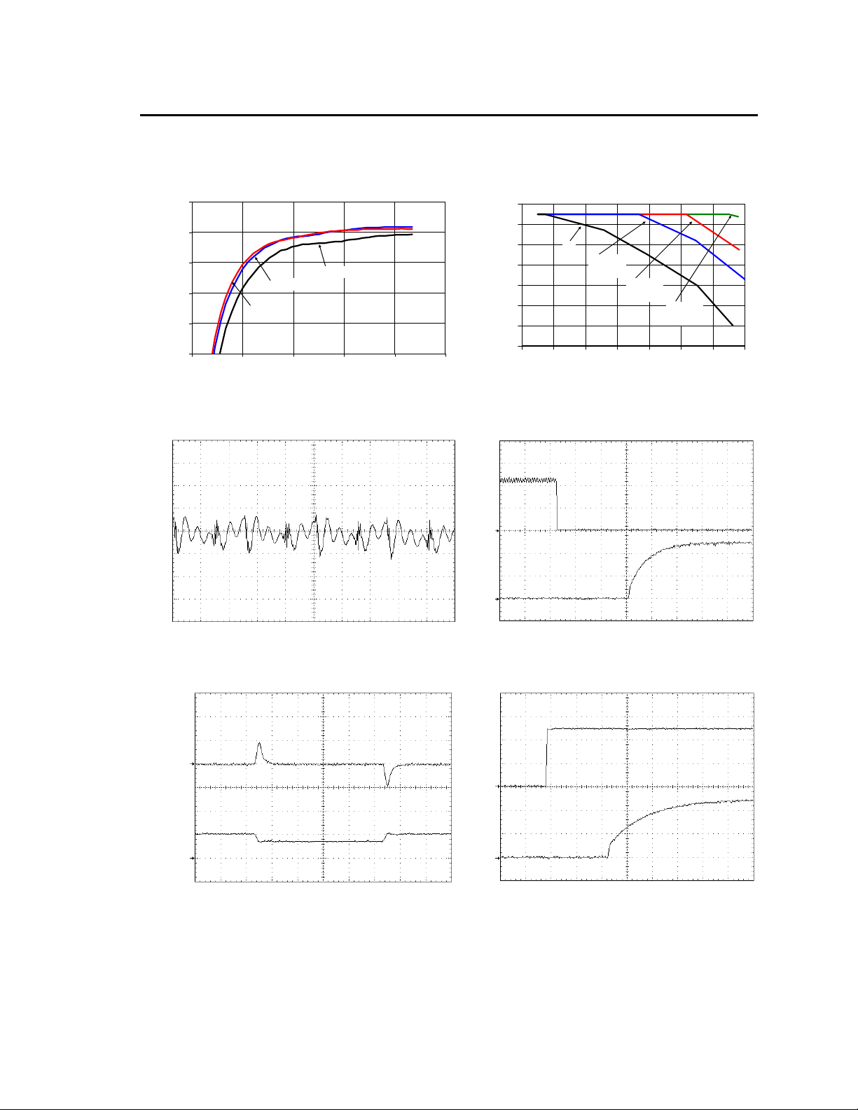
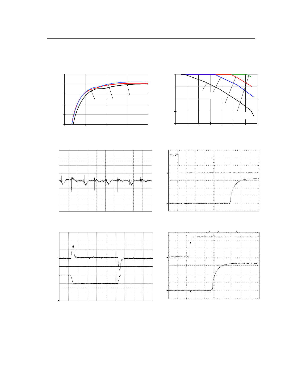
Characteristic Curves
The following figures provide typical characteristics for the KNW013A0A (5V, 13A) at 25oC. The figures are identical
for either positive or negative remote On/Off logic.
95
90
85
80
75
EFFICIENCY, (%)
70
03691215
Vin=48V
Vin=36V
OUTPUT CURRENT, IO (A) AMBIENT TEMPERATURE, TA OC
Vin=75V
14
12
10
8
6
4
2
NC
0.5 m/s
100 LFM
1.0 m/s
200 LFM
400 LFM
0
OUTPUT CURRENT, Io (A)
20 30 40 50 60 70 80 90
2.0 m/s
Figure 1. Converter Efficiency versus Output Current. Figure 4. Derating Output Current versus Local
Ambient Temperature and A i rflow.
(V) (2V/div)
On/off
(V) (20mV/div)
O
V
OUTPUT VOLTAGE
(V) (2V/div) V
TIME, t (1s/div)
Figure 2. Typical output ripple and noise (V
I
o = Io,max).
(V) (200mV/div)
O
IN = VIN,NOM,
OUTPUT VOLTAGE On/Off VOLTAGE
O
V
TIME, t (10ms/div)
Figure 5. Typical Start-up Using Remote On/Off,
negative logic version shown (VIN = VIN,NOM, Io =
I
o,max).
(V) (20V/div)
IN
(V) (2V/div) V
OUTPUT CURRENT OUTPUT VOLTAGE
Io (A) (10A/div) V
TIME, t (200 s /div)
Figure 3. Transient Response to Dynamic Load
Change, 0.1A/µS, from 75% to 50% to 75% of full load.
O
OUTPUT VOLTAGE INPUT VOLTAGE
V
Figure 6. Typical Start-up Using Input Voltage (VIN =
V
IN,NOM, Io = Io,max).
TIME, t (5ms/div)
LINEAGE POWER 5
Page 6
Data Sheet
OUTPUT
CURRENT
OUTPUT
VOLTAGE
August 22, 2011
36 – 75V
KNW013-020 Series Power Modules; DC-DC Converters
Input; 3.3 to 5.0Vdc Output; 13 to 20A Output Current
dc
Characteristic Curves
The following figures provide typical characteristics for the KNW020A0F (3.3V, 20A) at 25
identical for either positive or negative remote On/Off logic.
95
20
O
C. The figures are
90
85
80
75
Vin=36V
Vin=48
EFFICIENCY, (%)
70
0 5 10 15 20
Vin=75V
15
NC
0.5 m/s
10
5
0
OUTPUT CURRENT, Io (A)
100 LFM
1.0 m/s
200 LFM
20 30 40 50 60 70 80 90
2.0 m/s
400 LFM
OUTPUT CURRENT, IO (A) AMBIENT TEMPERATURE, TA OC
Figure 7. Converter Efficiency versus Output Current. Figu re 10. Derating Output Current versus Local
Ambient Temperature and A i rflow.
(V) (2V/div)
On/off
(V) (20mV/div)
O
V
OUTPUT VOLTAGE
(V) (1V/div) V
O
TIME, t (1s/div)
Figure 8. Typical output ripple and noise (V
I
o = Io,max).
IN = VIN,NOM,
V
OUTPUT VOLTAGE On/Off VOLTAGE
TIME, t (5ms/div)
Figure 11. Typical Start-up Using Remote On/Off,
negative logic version shown (VIN = VIN,NOM, Io = Io,max).
(V) (20V/div)
(V) (100mV/div)
O
IN
(V) (1V/div) V
Io (A) (5A/div) V
TIME, t (200 s /div)
Figure 9. Transient Response to Dynamic Load
Change, 0.1A/µS, from 75% to 50% to 75% of full load.
O
OUTPUT VOLTAGE INPUT VOLTAGE
V
TIME, t (5ms/div)
Figure 12. Typical Start-up Using Input Voltage (VIN =
V
IN,NOM, Io = Io,max).
LINEAGE POWER 6
Page 7

Data Sheet
August 22, 2011
36 – 75V
KNW013-020 Series Power Modules; DC-DC Converters
Input; 3.3 to 5.0Vdc Output; 13 to 20A Output Current
dc
Test Configurations
SCOPE
Vout+
Vout-
V
CURRENT PROBE
33μF
RESISTIVE
LOAD
R
contactRdistribution
O
R
contactRdistribution
x 100 %
Vin+
Vin-
R
LOAD
TO OSCILLOSCOPE
L
TEST
12μH
CS 220μF
BATTERY
NOTE: Measure input reflected ripple current with a simulated
E.S.R.<0.1
@ 20°C 100kHz
source inductance (L
possible battery impedance. Measure current as shown
above.
) of 12μH. Capacitor CS offsets
TEST
Figure 13. Input Reflected Ripple Current Test
Setup.
COPPER STRIP
V O (+)
V O ( – )
NOTE: All voltage measurements to be taken at the module
0.1uF
terminals, as shown above. If sockets are used then
Kelvin connections are requi red at the module terminals
to avoid measurement err ors due to socket contact
resistance.
10uF
GROUND PLANE
Figure 14. Output Ripple and Noise Test Setup.
R
R
contact
distribution
R
R
contact
distribution
NOTE: All voltage measurements to be taken at t he module
terminals, as shown above. If sockets are used then
Kelvin connections are required at the module terminals
to avoid measurement errors due to socket contact
resistance.
Vin+
V
IN
Vin-
Figure 15. Output Voltage and Efficiency Test
Setup.
V
. I
O
Efficiency
=
VIN. I
O
IN
Design Considerations
Input Filt ering
The power module should be connected to a low
ac-impedance source. Highly inductive source
impedance can affect the stability of the power
module. For the test configuration in Figure 13, a
33μF electrolytic capacitor (ESR<0.7 at 100kHz),
mounted close to the power module helps ensure the
stability of the unit. Consult the factory for further
application guidelines.
Safety Considerations
For safety-agency approval of the system in which the
power module is used, the power module must be
installed in compliance with the spacing and
separation requirements of the end-use safety agency
standard, i.e UL60950-1, CSA C22.2 No.60950-1,
and VDE0805-1(IEC60950-1).
If the input source is non-SELV (ELV or a hazardous
voltage greater than 60 Vdc and less than or equal to
75Vdc), for the module’s output to be considered as
meeting the requirements for safety extra-low voltage
(SELV), all of the following must be true:
The input source is to be provided with reinforced
insulation from any other hazardous voltages,
including the ac mains.
One V
pin and one V
IN
pin are to be
OUT
grounded, or both the input and output pins are
to be kept floating.
The input pins of the module are not operator
accessible.
Another SELV reliability test is conducted on the
whole system (combination of supply source and
subject module), as required by the safety
agencies, to verify that under a single fault,
hazardous voltages do not appear at the
module’s output.
Note: Do not ground either of the input pins of the
module without grounding one of the output
pins. This may allow a non-SELV voltage to
appear between the output pins and ground.
The power module has extra-low voltage (ELV)
outputs when all inputs are ELV.
All flammable materials used in the manufacturing of
these modules are rated 94V-0, or tested to the
UL60950 A.2 for reduced thickness.
For input voltages exceeding –60 Vdc but less than or
equal to –75 Vdc, these converters have been
evaluated to the applicable requirements of BASIC
INSULATION between secondary DC MAINS
DISTRIBUTION input (classified as TNV-2 in Europe)
and unearthed SELV outputs.
The input to these units is to be provided with a
maximum 5 A time-delay fuse in the ungrounded lead.
LINEAGE POWER 7
Page 8

Data Sheet
E
August 22, 2011
36 – 75V
KNW013-020 Series Power Modules; DC-DC Converters
Input; 3.3 to 5.0Vdc Output; 13 to 20A Output Current
dc
Feature Description
Remote On/Off
Two remote on/off options are available. Positive logic
turns the module on during a logic high voltage on the
ON/OFF pin, and off during a logic low. Negative logic
remote On/Off, device code suffix “1”, turns the
module off during a logic high and on during a logic
low.
Vin+
I
on/off
V
on/off
ON/OFF
Vin-
Figure 16. Remote On/Off Implementation.
To turn the power module on and off, the user must
supply a switch (open collector or equivalent) to
control the voltage (V
terminal and the V
low is 0V ≤ V
≤ 1.2V. The maximum I
on/off
) between the ON/OFF
on/off
(-) terminal (see Figure 16). Logic
IN
logic low is 1mA; the switch should be maintaining a
logic low level while sinking this current.
During a logic high, the typical maximum V
generated by the module is 15V, and the maximum
allowable leakage current at V
If not using the remote on/off feature:
For positive logic, leave the ON/OFF pin open.
For negative logic, short the ON/OFF pin to V
Remote Sense
Remote sense minimizes the effects of distribution
losses by regulating the voltage at the remote-sense
connections (See Figure 17). The voltage between
the remote-sense pins and the output terminals must
not exceed the output voltage sense range given in
the Feature Specifications table:
[VO(+) – VO(–)] – [SENSE(+) – SENSE(–)] 10% V
Although the output voltage can be increased by both
the remote sense and by the trim, the maximum
increase for the output voltage is not the sum of both.
The maximum increase is the larger of either the
remote sense or the trim.
The amount of power delivered by the module is
defined as the voltage at the output terminals
multiplied by the output current. When using remote
sense and trim, the output voltage of the module can
be increased, which at the same output current would
increase the power output of the module. Care should
Vout+
TRIM
Vout-
= 5V is 1μA.
on/off
on/off
on/off
during a
(-).
IN
O,set
be taken to ensure that the maximum output power of
the module remains at or below the maximum rated
power (Maximum rated power = V
SENSE(+)
SENSE(–)
V
I(+)
SUPPLY
CONTACT
RESISTANCE
I
I
VO(+)
I(-)
V
O(–)
V
x I
o,set
IO
DISTRIBUTION LOSS
).
o,max
LOAD
CONTACT AND
Figure 17. Circuit Configuration for remote
sense.
Input Undervoltage Lockout
At input voltages below the input undervoltage lockout
limit, the module operation is disabled. The module
will only begin to operate once the input voltage is
raised above the undervoltage lockout turn-on
threshold, V
UV/ON
.
Once operating, the module will continue to operate
until the input voltage is taken below the undervoltage
turn-off threshold, V
UV/OFF
.
Overtemperature Protection
To provide protection under certain fault conditions,
the unit is equipped with a thermal shutdown circuit.
The unit will shutdown if the thermal reference point
T
(Figure 19), exceeds 128-133oC (typical)
ref
depending on T
and airflow, but the thermal
A
shutdown is not intended as a guarantee that the unit
will survive temperatures beyond its rating. The
module will automatically restart upon cool-down to a
safe temperature.
Output Overvoltage Protection
The output over voltage protection scheme of the
modules has an independent over voltage loop to
prevent single point of failure. This protection feature
latches in the event of over voltage across the output.
Cycling the on/off pin or input voltage resets the
latching protection feature. If the auto-restart option
(4) is ordered, the module will automatically restart
upon an internally programmed time elapsing.
Overcurrent Protection
To provide protection in a fault (output overload)
condition, the unit is equipped with internal
current-limiting circuitry and can endure current
limiting continuously. At the point of current-limit
inception, the unit enters hiccup mode. If the unit is
not configured with auto–restart, then it will latch off
following the over current condition. The module can
be restarted by cycling the dc input power for at least
one second, or by toggling the remote on/off signal for
at least one second. If the unit is configured with the
LINEAGE POWER 8
Page 9

Data Sheet
August 22, 2011
36 – 75V
KNW013-020 Series Power Modules; DC-DC Converters
Input; 3.3 to 5.0Vdc Output; 13 to 20A Output Current
dc
Feature Descriptions (continued)
auto-restart option (4), it will remain in the hiccup
mode as long as the overcurrent condition exists; it
operates normally, once the output current is brought
back into its specified range. The average output
current during hiccup is 10% I
Output Voltage Programming
Trimming allows the output voltage set point to be
increased or decreased. This is accomplished by
connecting an external resistor between the TRIM pin
and either the V
VIN(+)
ON/OFF
VIN(-)
Figure 18. Circuit Configuration to Trim Output
Voltage.
Connecting an external resistor (R
the TRIM pin and the Vo(-) (or Sense(-)) pin
decreases the output voltage set point. To maintain
set point accuracy, the trim resistor tolerance should
be ±1.0%.
The following equation determines the required
external resistor value to obtain a percentage output
voltage change of Δ%
Where
For example, to trim-down the output voltage of 3.3V
module (KNW020A0F/F1) by 8% to 3.036V, R
is calculated as follows:
R
Connecting an external resistor (R
TRIM pin and the V
the output voltage set point. The following equations
determine the required external resistor value to
obtain a percentage output voltage change of Δ%:
(+) pin or the VO(-) pin.
O
VO(+)
VOTRIM
VO(-)
511
R
downtrim
downtrim
VV
,
desiredseto
V
,
seto
511
8
R
downtrim
(+) (or Sense (+)) pin increases
O
.
O, max
R
trim-up
LOAD
R
trim-down
) between
trim-down
%
22.10
100%
trim-down
8%
22.10
6.53
) between the
trim-up
R
Where
V
uptrim
,seto
V
,
%)100(11.5
511
%225.1
VV
,
setodesired
seto
%
100%
22.10
For example, to trim-up the output voltage of 5.0V
module (KNW013A0A/A1) by 5% to 5.25V, R
trim-up
is
calculated is as follows:
5%
511
R
uptrim
)5100(0.511.5
5225.1
5
22.10
R
uptrim
The voltage between the Vo(+) and Vo(–) terminals
6.325
must not exceed the minimum output overvoltage
protection value shown in the Feature Specifications
table. This limit includes any increase in voltage due
to remote-sense compensation and output voltage
set-point adjustment trim.
Although the output voltage can be increased by both
the remote sense and by the trim, the maximum
increase for the output voltage is not the sum of both.
The maximum increase is the larger of either the
remote sense or the trim. The amount of power
delivered by the module is defined as the voltage at
the output terminals multiplied by the output current.
When using remote sense and trim, the output
voltage of the module can be increased, which at the
same output current would increase the power output
of the module. Care should be taken to ensure that
the maximum output power of the module remains at
or below the maximum rated power (Maximum rated
power = V
o,set
x I
o,max
).
Thermal Considerations
The power modules operate in a variety of thermal
environments; however, sufficient cooling should be
provided to help ensure reliable operation.
Considerations include ambient temperature, airflow,
module power dissipation, and the need for increased
reliability. A reduction in the operating temperature of
the module will result in an increase in reliability. The
thermal data presented here is based on physical
measurements taken in a wind tunnel.
The thermal reference points, Tref
, used in the
x
specifications are shown in Figure 19. For reliable
operation, the temperature of both Tref points should
not exceed 125
o
C.
LINEAGE POWER 9
Page 10

Data Sheet
August 22, 2011
36 – 75V
KNW013-020 Series Power Modules; DC-DC Converters
dc
Thermal Considerations (continued)
Input; 3.3 to 5.0Vdc Output; 13 to 20A Output Current
Figure 21. KNW020A0F Quasi Peak Conducted
Emissions with EN 55022 Class A limits, Figure 20
filter (V
IN
= V
IN,NOM
, Io = 0.80 I
o,max
).
Layout Considerations
Avoid placing copper areas on the outer layer of the
application PCB directly underneath the power
module in the keep out areas shown in the
Recommended Pad Layout figures. Also avoid
placing via interconnects underneath the power
module in these keep out areas.
Figure 19. Tref
Location.
Please refer to the Application Note “Thermal
Characterization Process For Open-Frame BoardMounted Power Modules” for a detailed discussion of
thermal aspects including maximum device
temperatures.
Temperature Measurement
x
EMC Considerations
The KNW series module shall also meet limits of
EN55022 Class A with a recommended single stage
filter, shown in Figure 20. Please contact your
Lineage Power Sales Representative for further
information.
Figure 20. Single stage filter used for test results.
LINEAGE POWER 10
Page 11

Data Sheet
August 22, 2011
36 – 75V
KNW013-020 Series Power Modules; DC-DC Converters
Input; 3.3 to 5.0Vdc Output; 13 to 20A Output Current
dc
Surface Mount Information
Pick and Place
The KNW013-020 modules use an open frame
construction and are designed for a fully automated
assembly process. The pick and place locations on
the module are the larger magnetic core or the
transistor package as shown in Figure 22. The
modules are fitted with a label which meets all the
requirements for surface mount processing, as well as
safety standards, and is able to withstand reflow
temperatures of up to 300
product information such as product code, serial
number and the location of manufacture.
Figure 22. Pick and Place Locations.
Nozzle Recommendations
The module weight has been kept to a minimum by
using open frame construction. Even so, these
modules have a relatively large mass when compared
to conventional SMT components. Variables such as
nozzle size, tip style, vacuum pressure and placement
speed should be considered to optimize this process.
The recommended nozzle diameter for reliable
operation is 5mm. Oblong or oval nozzles up to 11 x 5
mm may also be used within the space available.
Tin Lead Soldering
The KNW013-020 power modules (both non-Z and –Z
codes) can be soldered either in a conventional
Tin/Lead (Sn/Pb) process. The non-Z version of the
KNW013-020 modules are RoHS compliant with the
lead exception. Lead based solder paste is used in
the soldering process during the manufacturing of
these modules. These modules can only be soldered
in conventional Tin/lead (Sn/Pb) process. It is
recommended that the customer review data sheets
in order to customize the solder reflow profile for each
application board assembly. The following
instructions must be observed when soldering these
units. Failure to observe these instructions may result
in the failure of or cause damage to the modules, and
can adversely affect long-term reliability.
o
C. The label also carries
In a conventional Tin/Lead (Sn/Pb) solder process
peak reflow temperatures are limited to less than
o
235
C. Typically, the eutectic solder melts at 183oC,
wets the land, and subsequently wicks the device
connection. Sufficient time must be allowed to fuse
the plating on the connection to ensure a reliable
solder joint. There are several types of SMT reflow
technologies currently used in the industry. These
surface mount power modules can be reliably
soldered using natural forced convection, IR (radiant
infrared), or a combination of convection/IR. For
reliable soldering the solder reflow profile should be
established by accurately measuring the modules CP
connector temperatures.
300
250
200
15 0
10 0
REFLOW TEMP (C)
50
0
Peak Temp 235oC
Heat zone
oCs-1
max 4
So ak zone
30-240s
Preheat zo ne
oCs-1
max 4
REFLOW TIME (S)
T
lim
205
Co o ling
zo ne
1- 4
above
o
C
oCs-1
Figure 23. Reflow Profile for Tin/Lead (Sn/Pb)
process
240
235
230
225
220
215
210
MAX TEMP SOLDER (C)
205
200
0 102030405060
Figure 24. Time Limit Curve Above 205oC for
Tin/Lead (Sn/Pb) process
LINEAGE POWER 11
Page 12

Data Sheet
August 22, 2011
36 – 75V
KNW013-020 Series Power Modules; DC-DC Converters
Input; 3.3 to 5.0Vdc Output; 13 to 20A Output Current
dc
Surface Mount Information (continued)
Lead Free Soldering
The –Z version of the KNW013-020 modules are
lead-free (Pb-free) and RoHS compliant, and are both
forward and backward compatible in a Pb-free and a
SnPb soldering process. The non-Z version of the
KNW006/010 modules are RoHS compliant with the
lead exception. Lead based solder paste is used in
the soldering process during the manufacturing of
these modules. These modules can only be soldered
in conventional Tin/lead (Sn/Pb) process. Failure to
observe the instructions below may result in the
failure of or cause damage to the modules and can
adversely affect long-term reliability.
Pb-free Reflow Profile
Power Systems will comply with J-STD-020 Rev. C
(Moisture/Reflow Sensitivity Classification for
Nonhermetic Solid State Surface Mount Devices) for
both Pb-free solder profiles and MSL classification
procedures. This standard provides a recommended
forced-air-convection reflow profile based on the
volume and thickness of the package (table 4-2). The
suggested Pb-free solder paste is Sn/Ag/Cu (SAC).
The recommended linear reflow profile using
Sn/Ag/Cu solder is shown in Figure 25.
MSL Rating
The KNW013-020 modules have a MSL rating of 3.
Storage and Handling
The recommended storage environment and handling
procedures for moisture-sensitive surface mount
packages is detailed in J-STD-033 Rev. A (Handling,
Packing, Shipping and Use of Moisture/Reflow
Sensitive Surface Mount Devices). Moisture barrier
bags (MBB) with desiccant are required for MSL
ratings of 2 or greater. These sealed packages
should not be broken until time of use. Once the
original package is broken, the floor life of the product
at conditions of
varies according to the MSL rating (see J-STD-033A).
The shelf life for dry packed SMT packages will be a
minimum of 12 months from the bag seal date, when
stored at the following conditions: < 40° C, < 90%
relative humidity.
30°C and 60% relative humidity
300
Per J-STD-020 Rev. C
250
200
150
100
Reflow Temp (°C)
50
0
Heat ing Zone
1°C/Second
Peak Temp 260°C
* Min. Time Above 235°C
15 Seconds
*Time Above 217°C
60 Seconds
Reflow Time (Seconds)
Cooling
Zone
Figure 25. Recommended linear reflow profile
using Sn/Ag/Cu solder.
Through-Hole Lead-Free Soldering
Information
The RoHS-compliant through-hole products use the
SAC (Sn/Ag/Cu) Pb-free solder and RoHS-compliant
components. They are designed to be processed
through single or dual wave soldering machines. The
pins have an RoHS-compliant finish that is compatible
with both Pb and Pb-free wave soldering processes.
A maximum preheat rate of 3
wave preheat process should be such that the
temperature of the power module board is kept below
C. For Pb solder, the recommended pot
210
temperature is 260
C, and, for Pb-free solder, the
recommended pot temperature is 270
RoHS-compliant through-hole products can be
processed with paste-through-hole Pb or Pb-free
reflow process. If additional information is needed,
please consult with your Lineage Power
representative for more details.
C/s is suggested. The
C max. Not all
Post Solder Cleaning and Drying
Considerations
Post solder cleaning is usually the final circuit-board
assembly process prior to electrical board testing. The
result of inadequate cleaning and drying can affect
both the reliability of a power module and the
testability of the finished circuit-board assembly. For
guidance on appropriate soldering, cleaning and
drying procedures, refer to Lineage Power Board
Mounted Power Modules: Soldering and Cleaning
Application Note (AN04-001).
LINEAGE POWER 12
Page 13

Data Sheet
August 22, 2011
36 – 75V
KNW013-020 Series Power Modules; DC-DC Converters
Input; 3.3 to 5.0Vdc Output; 13 to 20A Output Current
dc
Mechanical Outline for Surface Mount Module
Dimensions are in millimeters and [inches].
Tolerances: x.x mm
x.xx mm
0.5 mm [x.xx in. 0.02 in.] (unless otherwise indicated)
0.25 mm [x.xxx in 0.010 in.]
Top View
Side View
Bottom View
PIN FUNCTION
1 VIN(+)
2 On/Off
3 VIN(-)
4 Vo(-)
5 Sense(-)
6 Trim
7 Sense(+)
8 Vo(+)
LINEAGE POWER 13
Page 14

Data Sheet
August 22, 2011
36 – 75V
KNW013-020 Series Power Modules; DC-DC Converters
Input; 3.3 to 5.0Vdc Output; 13 to 20A Output Current
dc
Mechanical Outline for Through-Hole Module
Dimensions are in millimeters and [inches].
Tolerances: x.x mm
x.xx mm
0.5 mm [x.xx in. 0.02 in.] (unless otherwise indicated)
0.25 mm [x.xxx in 0.010 in.]
Top View
Side View
Bottom View
PIN FUNCTION
1 VIN(+)
2 On/Off
3 VIN(-)
4 Vo(-)
5 Sense(-)
6 Trim
7 Sense(+)
8 Vo(+)
LINEAGE POWER 14
Page 15

Data Sheet
August 22, 2011
36 – 75V
Recommended Pad Layout
Dimensions are in and millimeters [inches].
Tolerances: x.x mm
x.xx mm
0.5 mm [x.xx in. 0.02 in.] (unless otherwise indicated)
0.25 mm [x.xxx in 0.010 in.]
KNW013-020 Series Power Modules; DC-DC Converters
Input; 3.3 to 5.0Vdc Output; 13 to 20A Output Current
dc
SMT Recommended Pad Layout (Component Side View)
TH Recommended Pad Layout (Component Side View)
LINEAGE POWER 15
Page 16

Data Sheet
August 22, 2011
36 – 75V
KNW013-020 Series Power Modules; DC-DC Converters
Input; 3.3 to 5.0Vdc Output; 13 to 20A Output Current
dc
Packaging Details
The Sixteenth-brick SMT versions are supplied in tape & reel as standard. Details of tape dimensions are shown
below. Modules are shipped in quantities of 140 modules per reel.
Tape Dimensions
Dimensions are in millimeters.
LINEAGE POWER 16
Page 17

Data Sheet
a
©
August 22, 2011
36 – 75V
KNW013-020 Series Power Modules; DC-DC Converters
Input; 3.3 to 5.0Vdc Output; 13 to 20A Output Current
dc
Ordering Information
Please contact your Lineage Power Sales Representative for pricing, availability and optional features.
Table 1. Device Code
Product Codes Input Voltage
Output
Voltage
KNW013A0A4-SRZ 48V (36-75Vdc) 5.0V 13A Negative Surface mount CC109167128
KNW013A0A41-SRZ 48V (36-75Vdc) 5.0V 13A Negative Surface mount CC109141438
KNW013A0A41Z 48V (36-75Vdc) 5.0V 13A Negative Through hole CC109141446
KNW013A0A641Z 48V (36-75Vdc) 5.0V 13A Negative Through hole CC109156948
KNW013A0A841Z 48V (36-75Vdc) 5.0V 13A Negative Through hole CC109160207
KNW020A0F1-SRZ 48V (36-75Vdc) 3.3V 20A Negative Surface mount CC109172292
KNW020A0F41-SRZ 48V (36-75Vdc) 3.3V 20A Negative Surface mount CC109139267
KNW020A0F41Z 48V (36-75Vdc) 3.3V 20A Negative Through hole CC109139275
KNW020A0F641Z 48V (36-75Vdc) 3.3V 20A Negative Through hole CC109155727
KNW020A0F841Z 48V (36-75Vdc) 3.3V 20A Negative Through hole CC109167350
Table 2. Device Coding Scheme and Options
Characteristic Definition
Form Fact or K K = Sixteenth Bric k
Family Designator N
Input Vol tage W W = Wide Range, 36V-75V
Output Current
Ratings
Output Voltage
Pin Length
Action following
Protect ive Shutdown
On/Off Logic
Options
Mechanic al Features
Customer Specific XY XY = Customer Specific Modified Code, Omit for Standard Code
RoHS
Character and Posit i on
013A0 013A0 = 013.0 Amps Max imum Output Current
020A0 020A0 = 020.0 Amps Max imum Output Current
A A = 5.0V nominal
F F = 3.3V nominal
6 6 = Pin Length: 3. 68 mm ± 0.25m m , (0.145 in. ± 0. 010 in. )
8 8 = Pin Length: 2. 79 mm ± 0.25m m , (0.110 in. ± 0. 010 in. )
4 4 = Aut o-rest art following shut down (Overcurrent/ Overvoltage)
1 1 = Negative Logic
Output
Current
Omit = Default Pin Length shown in Mechanical Outline Figures
Omit = Latc hing Mode
Omit = Positive Logic
Omit = Standard open Fram e Module
SR SR = Surface mount connect ions & t ape/reel package
Omit = RoHS 5/6, Lead Based S older Us ed
Z Z = RoHS 6/6 Compliant , Lead free
On/Off Logic
Connector
Type
Comcode
Asia-Pacific Headquarters
Tel: +86.021.54279977*808
World Wide Headquarters
Lineage Power Corporation
601 Shiloh Road, Plano, TX 75074, USA
+1-888-LINEAGE(546-3243)
(Outside U.S.A.: +1-972-244-WATT(9288))
www.lineagepower.com
e-mail: techsupport1@lineagepower.com
Europe, Middle-East and Africa Headquarters
Tel: +49.89.878067-280
India Headquarters
Tel: +91.80.28411633
Lineage Power reserves the right to make changes to the produ ct(s) or information contained herein without notice. No liability is assumed as a re sult of their use or
pplication. No rights under any patent accompany the sale of any such p roduct(s) or information.
Lineage Power DC-DC products are protected under various paten ts. Information on these patents is available at www.lineagepower.com/patents.
2010 Lineage Power Corporation, (Plano, Texas) All Internatio nal Rights Reserved.
Document No: DS08-009 ver. 1.05
PDF name: knw013-020_ds.pdf
 Loading...