

Page 1
GE
Data Sheet
KHHD015A0F Hammerhead™ Series; DC-DC Converter Power Modules
18-75Vdc Input; 3.3Vdc, 12A/15A Output
RoHS Compliant
Applications
Wireless Networks
Hybrid power architectures
Optical and Access Network Equipment
Enterprise Networks including Power over Ethernet (PoE)
Industrial markets
Options
Negative Remote On/Off logic (preferred)
Surface Mount/Tape and Reel (-SR Suffix)
Auto-restart Over current/Over voltage protections
(preferred)
Shorter through hole pin trim
Features
Compliant to RoHS II EU “Directive 2011/65/EU (-Z versions)
Compliant to REACH Directive (EC) No 1907/2006
Ultra-wide Input Voltage Range, 18V
No minimum load
High efficiency – 90.5% at full load (V
Constant switching frequency
Low output ripple and noise
Small Size and low profile, follows DOSA standard 1/16th
footprint
33.0 mm x 22.9 mm x 9.3 mm
(1.30 in x 0.9 in x 0.37 in)
Surface mount (SMT) or Through hole (TH)
Reflow process compliant, both SMT and TH versions
Positive Remote On/Off logic
Output overcurrent/voltage protection (hiccup)
Over-temperature protection
Output Voltage adjust: 80% to 110% of V
Wide operating temperature range (-40°C to 85°C)
UL*Recognized to UL60950-1, CAN/CSA
and EN60950-1(VDE
‡
0805-1) Licensed
CE mark meets 2006/95/EC directive
Meets the voltage and current requirements for ETSI 300-
132-2 and complies with and licensed for Basic insulation
rating per EN60950-1
2250 Vdc Isolation tested in compliance with IEEE 802.3
PoE standards
ISO** 9001 and ISO 14001 certified manufacturing facilities
to 75Vdc
dc
=48Vdc)
IN
o,nom
†
C22.2 No.60950-1,
§
¤
Description
The KHHD015A0F series power modules are isolated DOSA compliant 1/16th brick dc-dc converters that operate over an ultrawide input voltage range of 18 V
-75Vdc and provide a single precisely regulated output voltage at 3.3Vdc. The output is fully
dc
isolated from the input, allowing versatile polarity configurations and grounding connections. The modules exhibit high efficiency
of 90.5% typical at full load. Built-in filtering for both input and output minimizes the need for external filtering. The module is fully
self-protected with output over-current and over-voltage, over-temperature and input under voltage shutdown control. Optional
features include negative or positive on/off logic and SMT connections
* UL is a registered trademark of Underwriters Laboratories, Inc.
†
CSA is a registered trademark of Canadian Standards Association.
‡
VDE is a trademark of Verband Deutscher Elektrotechniker e.V.
§ This product is intended for integration into end-user equipment. All of the required procedures of end-use equipment should be followed.
¤ IEEE and 802 are registered trademarks of the Institute of Electrical and Electronics Engineers, Incorporated.
** ISO is a registered trademark of the International Organization of Standards.
April 1, 2013 ©2012 General Electric Company. All rights reserved. Page 1
Page 2
GE
Data Sheet
KHHD015A0F Hammerhead™ Series; DC-DC Converter Power Modules
18-75Vdc Input; 3.3Vdc, 12A/15A Output
Absolute Maximum Ratings
Stresses in excess of the absolute maximum ratings can cause permanent damage to the device. These are absolute stress ratings
only, functional operation of the device is not implied at these or any other conditions in excess of those given in the operations
sections of the data sheet. Exposure to absolute maximum ratings for extended periods can adversely affect the device reliability.
Parameter Device Symbol Min Max Unit
Input Voltage (Continuous) All V
Transient (100ms) All V
Operating Ambient Temperature All T
(see Thermal Considerations section)
Storage Temperature All T
Altitude* All
I/O Isolation Voltage (100% factory Hi-Pot tested) All
IN
IN, trans
A
stg
* For higher altitude applications, contact your GE Sales Representative for alternative conditions of use.
Electrical Specifications
Unless otherwise indicated, specifications apply at VIN = 48Vdc, resistive load, and TA = 25°C conditions.
Parameter Device Symbol Min Typ Max Unit
Operating Input Voltage All VIN 18 24/48 75 Vdc
Input No Load Current
(VIN = 48Vdc IO = 0A, module enabled)
Input Stand-by Current
(VIN = 24 to 48Vdc, module disabled)
Maximum Input Current (VIN=18Vdc, IO= I
Inrush Transient All I2t 0.05 A2s
Input Reflected Ripple Current, peak-to-peak
(5Hz to 20MHz, 12μH source impedance; V
see Test configuration section)
Input Ripple Rejection (120Hz) All 60 dB
) All I
O,MAX
=0V to 75Vdc, IO= I
IN
Omax
;
All I
All I
All 30 mA
IN,No load
6 8 mA
IN,stand-by
IN, MAX
-0.3 80 Vdc
-0.3 100 Vdc
-40 85 °C
-55 125 °C
4000 m
2250 Vdc
40 50 mA
2.65 Adc
p-p
EMC, EN55022 See EMC Considerations section
CAUTION: This power module is not internally fused. An input line fuse must always be used.
This power module can be used in a wide variety of applications, ranging from simple standalone operation to being part of
complex power architecture. To preserve maximum flexibility, internal fusing is not included; however, to achieve maximum safety
and system protection, always use an input line fuse. The safety agencies require a fast-acting fuse with a maximum rating of 6A
(see Safety Considerations section). Based on the information provided in this data sheet on inrush energy and maximum dc input
current, the same type of fuse with a lower rating can be used. Refer to the fuse manufacturer’s data sheet for further information.
April 1, 2013 ©2012 General Electric Company. All rights reserved. Page 2
Page 3
GE
Data Sheet
KHHD015A0F Hammerhead™ Series; DC-DC Converter Power Modules
18-75Vdc Input; 3.3Vdc, 12A/15A Output
Electrical Specifications (continued)
Unless otherwise indicated, specifications apply at VIN = 48Vdc, resistive load, and TA = 25°C conditions.
Parameter Device Symbol Min Typ Max Unit
Output Voltage Set-point
=24 to 48Vdc, IO=I
(V
IN
O, max
,)
Output Voltage
(Over all operating input voltage, resistive load, and temperature
conditions until end of life)
Adjustment Range
Selected by external resistor
Remote Sense Range
Output Regulation
Line (VIN=V
Load (IO=I
Temperature (T
IN, min
O, min
to V
) All
IN, max
to I
) All
O, max
to T
ref=TA, min
) All
A, max
Output Ripple and Noise on nominal output
Measured with 10uF Tantalum||1uF ceramic
(VIN=24 to 48Vdc, IO=80%I
)
O, max
RMS (5Hz to 20MHz bandwidth)
Peak-to-Peak (5Hz to 20MHz bandwidth)
External Capacitance (see Note 1 in Feature Specifications) All C
Output Current
(VIN =36V to 75V) All I
(VIN =18V to 36V) All I
Output Current Limit Inception (Hiccup Mode)
(VIN =36V to 75V) All I
(VIN =18V to 36V) All I
Output Short-Circuit Current (VO ≤ 250 mV) All I
Efficiency (VIN=24Vdc, IO=I
Efficiency (VIN=48Vdc, IO=I
) All η 87.5 88.5
O, max
) All η 89.5 90.5
O, max
Switching Frequency (Fixed)
VIN=24 to 48Vdc, IO= I
O, max
Dynamic Load Response
(Io/t=0.1A/s)
Load Change from Io= 50% to 75% or 25% to 50% of I
:
o,max
Peak Deviation All Vpk
Settling Time (Vo<10% peak deviation) All ts
All V
All V
All V
All
O, set
O
O, adj
+10 % V
All
All f
O, max
o
o
O, lim
O, lim
O, s/c
sw
3.25 3.30 3.35 Vdc
-3.0
-20
0
0.05 0.2 % V
0.05 0.2 % V
+3.0 % V
+10 % V
1.0 % V
25 mV
75 mV
5000 μF
O, set
O, set
O, set
O, set
O, set
O, set
rms
pk-pk
0
0
15.0 Adc
12.0 Adc
16.5
13.2
2.5
450
21 Adc
16.5 Adc
A
rms
%
%
kHz
3.0
400
% V
O, set
s
Isolation Specifications
Parameter Symbol Min Typ Max Unit
Isolation Capacitance C
Isolation Resistance R
I/O Isolation Voltage All
iso
iso
10
1000
2250 Vdc
April 1, 2013 ©2012 General Electric Company. All rights reserved. Page 3
pF
MΩ
Page 4
GE
Data Sheet
KHHD015A0F Hammerhead™ Series; DC-DC Converter Power Modules
18-75Vdc Input; 3.3Vdc, 12A/15A Output
General Specifications
Parameter
Calculated Reliability based upon Telcordia SR-332 Issue 2: Method I Case 3
(I
O
=80%I
, TA=40°C, airflow = 200 lfm, 90% confidence)
O, max
Weight
FIT 274.7 10
MTBF 3,640,826 Hours
Min Typ Max Unit
9
/Hours
13 (0.46)
g (oz.)
Feature Specifications
Unless otherwise indicated, specifications apply at VIN = 48Vdc, resistive load, and TA = 25°C conditions. See Feature Descriptions for
additional information.
Parameter Device Symbol Min Typ Max Unit
Remote On/Off Signal Interface
(VIN=V
Signal referenced to V
Negative Logic: device code suffix “1”
Logic Low = module On, Logic High = module Off
Positive Logic: No device code suffix required
Logic Low = module Off, Logic High = module On
Turn-On Delay and Rise Times
(IO=80% of I
Case 1: Input power is applied for at least 1second, and then the
On/Off input is set from OFF to ON (T
V
O
to V
IN, min
Logic Low - Remote On/Off Current (V
; open collector or equivalent,
IN, max
terminal)
IN-
= -0.7Vdc) All I
on/off
Logic Low - On/Off Voltage All V
Logic High Voltage (I
= 0Adc) All V
on/off
Logic High maximum allowable leakage current All I
)
O, max
= 10% of V
O, set
= on/off pin transition until
delay
)
All
on/off
on/off
on/off
on/off
T
Case1
delay
-0.7
2.4
0.15 mA
0.8 Vdc
7 Vdc
25 μA
35 50 ms
Case 2: On/Off input is set to Module ON, and then input power is
applied
= VIN reaches V
(T
delay
until VO = 10% of V
IN, min
O,set
)
Output voltage Rise time (time for Vo to rise from 10%
of V
to 90% of V
o,set
o, set
)
All
All T
Output Voltage Overshoot
(IO=80% of I
Output Overvoltage Protection
, VIN= 24 to 48Vdc)
O, max
All V
Input Undervoltage Lockout
Turn-on Threshold All V
Turn-off Threshold All V
Hysterisis All V
T
delay
Case2
O, limit
uv/on
uv/off
rise
hyst
4.0
14 15
24 50 ms
30 50 ms
3 % V
5.5 Vdc
17 18 V
2.0
Vdc
Vdc
O, set
dc
Note: 1.The module requires a minimum of 470 μF external output capacitor to avoid exceeding the OVP maximum limits during startup into open
loop fault conditions.
April 1, 2013 ©2012 General Electric Company. All rights reserved. Page 4
Page 5
G
K
1
A
C
T
e
On/Off VOLTAGE OUTPUT VOLTAGE
E
1
n
s
o
v
i
c
a
d
s
m
U
n
M
s
2
A
2
g
A
t
O
=
e
e
e
v
C
A
F
e
e
g
e
n
e
r
o
a
P
e
L
t
5
0
%
2
n
h
o
d
m
V
5
=
Data S
eet
HHD0
8-75Vdc I
haracteri
he following fi
ither positive
EFFICIENCY, (%)
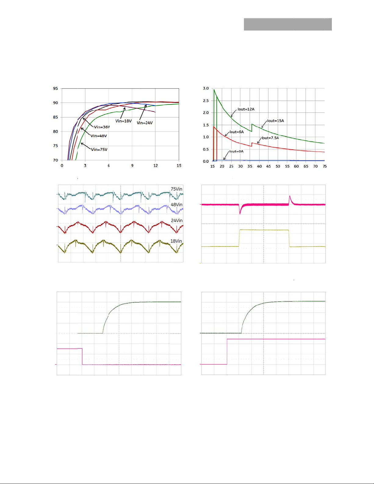
Figure 1. Con
5A0F H
put; 3.3V
tic Curve
gures provide
r negative re
OUTP
verter Efficie
mmerh
c, 12A/15
typical charac
ote On/Off lo
T CURRENT, IO (
cy versus Ou
ead™ S
Output
teristics for th
ic.
)
put Current.
ries; D
KHHD015A0
Figur
(A)
IN
INPUT CURRENT, I
(V) (100mV/div)
O
-DC Co
(3.3V, 12A/15
2. Converte
verter
A) at 25oC. Th
INPUT VO
Input Curren
ower M
figures are i
TAGE, VIN (V)
versus Input
dules
entical for
Voltage.
(V) (50mV/div)
O
V
OUTPUT VOLTAGE
Figure 3. Typ
( (V) (1V/div)
O
V) (2V/div) V
On/Off
V
Figure 5.Typi
logic version
cal output rip
al Start-up U
shown (VIN =
TI
ME, t (1s/div)
ple and noise
TI
E, t (20ms/div)
ing Remote
4V or 48V, Io
(Io = I
o,max
).
n/Off, negati
I
).
o,max
OUTPUT CURRENT OUTPUT VOLTAGE
Figur
Chan
INPUT VOLTAGE OUTPUT VOLTAGE
e Figur
I
o,max
Io(A) (2A/div) V
4. Transient
e from 50% t
(V) (1V/div)
O
(V) (20V/div) V
IN
V
6. Typical St
).
TIME, t (
Response to
75% to 50
TIME, t (
rt-up Using I
00s/div)
.1A/µS Dyna
of full load,
0ms/div)
put Voltage (
ic Load
in=48V.
V
IN
= 48V, I
o
pril 1, 2013
©
012 General El
ctric Company.
ll rights reserv
d.
Page
Page 6

GE
Data Sheet
KHHD015A0F Hammerhead™ Series; DC-DC Converter Power Modules
18-75Vdc Input; 3.3Vdc, 12A/15A Output
Test Configurations
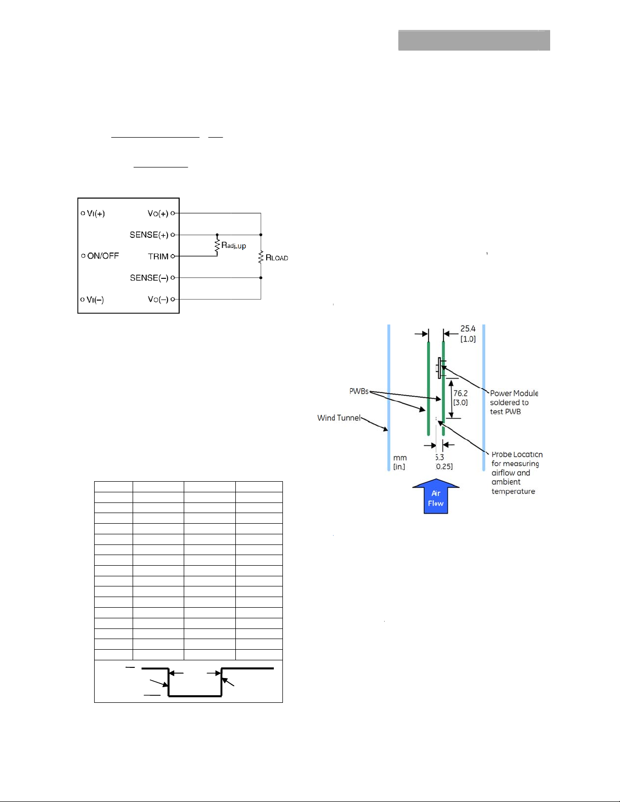
Vout+
V
Vout-
x 100 %
CURRENT PROBE
33μF
SC O PE
O
Vin+
Vin-
RESISTI V E
LO A D
R
contact Rdistribution
R
contact Rdistribution
R
TO OSCILLOSCOPE
L
TEST
12μH
CS 220μF
BATTERY
NOTE: Measure input reflected ripple current with a simulated
E.S.R.<0.1
@ 20°C 100kHz
source inductance (L
possible battery impedance. Measure current as shown
above.
) of 12μH. Capacitor CS offsets
TEST
Figure 7. Input Reflected Ripple Current Test Setup.
C OP PER STRIP
V
(+)
O
1uF .
V
( – )
O
NOTE: All voltage measurements to be taken at the module
terminals, as shown above. If sockets are used then
Kelvin connections are required at the module terminals
to avoid measurement errors due to socket contact
resistance.
10uF
GROUND PLANE
Figure 8. Output Ripple and Noise Test Setup.
R
R
contact
distribution
R
R
contact
distribution
NOTE: All voltage measurements to be taken at the module
terminals, as shown above. If sockets are used then
Kelvin connections are required at the module terminals
to avoid measurement errors due to socket c ontact
resistance.
Vin+
V
IN
Vin-
Figure 9. Output Voltage and Efficiency Test Setup.
. I
V
O
Efficiency
=
VIN. I
O
IN
LOAD
Design Considerations
Input Source Impedance
The power module should be connected to a low
ac-impedance source. Highly inductive source impedance can
affect the stability of the power module. For the test
configuration in Figure 7, a 33μF electrolytic capacitor
(ESR<0.7 at 100kHz), mounted close to the power module
helps ensure the stability of the unit. Consult the factory for
further application guidelines.
Safety Considerations
For safety-agency approval of the system in which the power
module is used, the power module must be installed in
compliance with the spacing and separation requirements of
the end-use safety agency standard, i.e., UL 60950-1-3, CSA
C22.2 No. 60950-00, and VDE 0805 (IEC60950, 3
If the input source is non-SELV (ELV or a hazardous voltage
greater than 60 Vdc and less than or equal to 75Vdc), for the
module’s output to be considered as meeting the requirements
for safety extra-low voltage (SELV), all of the following must be
true:
The input source is to be provided with reinforced
insulation from any other hazardous voltages, including
the ac mains.
One V
pin and one V
IN
the input and output pins are to be kept floating.
The input pins of the module are not operator accessible.
Another SELV reliability test is conducted on the whole
system (combination of supply source and subject
module), as required by the safety agencies, to verify that
under a single fault, hazardous voltages do not appear at
the module’s output.
Note: Do not ground either of the input pins of the module
without grounding one of the output pins. This may
allow a non-SELV voltage to appear between the output
pins and ground.
The power module has extra-low voltage (ELV) outputs when all
inputs are ELV.
For input voltages exceeding –60 Vdc but less than or equal to
–75 Vdc, these converters have been evaluated to the
applicable requirements of BASIC INSULATION between
secondary DC MAINS DISTRIBUTION input (classified as TNV-2
in Europe) and unearthed SELV outputs.
The input to these units is to be provided with a maximum 6A
fast acting fuse in the ungrounded lead.
pin are to be grounded, or both
OUT
rd
Edition).
April 1, 2013 ©2012 General Electric Company. All rights reserved. Page 6
Page 7

GE
Data Sheet
KHHD015A0F Hammerhead™ Series; DC-DC Converter Power Modules
18-75Vdc Input; 3.3Vdc, 12A/15A Output
Feature Description
Remote On/Off
Two remote on/off options are available. Positive logic turns
the module on during a logic high voltage on the on/off pin,
and off during a logic low. Negative logic remote on/off, device
code suffix “1”, turns the module off during a logic high and on
during a logic low.
Vin+
I
on/off
V
on/off
ON/OFF
Vin-
Figure 10. Circuit configuration for using Remote On/Off
Implementation.
To turn the power module on and off, the user must supply a
switch (open collector or equivalent) to control the voltage
) between the ON/OFF terminal and the VIN(-) terminal.
(V
on/off
Logic low is 0V ≤ V
≤ 0.8V. The maximum I
on/off
logic low is 0.15mA, the switch should be maintain a logic low
level whilst sinking this current.
During a logic high, the typical V
is 4.0V, and the maximum allowable leakage current at V
4.0V is 25μA.
If not using the remote on/off feature:
For positive logic, leave the ON/OFF pin open.
For negative logic, short the ON/OFF pin to V
Overcurrent Protection
To provide protection in a fault (output overload) condition, the
unit is equipped with internal current-limiting circuitry and can
endure current limiting continuously. At the point of
current-limit inception, the unit enters hiccup mode. If the unit
is not configured with auto–restart, then it will latch off
following the over current condition. The module can be
restarted by cycling the dc input power or by toggling the
remote on/off signal. If the unit is configured with the autorestart option (4), it will remain in the hiccup mode as long as
the overcurrent condition exists; it operates normally, once the
output current is brought back into its specified range.
Overtemperature Protection
To provide protection under certain fault conditions, the unit is
equipped with a thermal shutdown circuit. The unit will shut
down if the thermal reference point Tref (Figure 16), exceeds
o
C (typical), but the thermal shutdown is not intended as a
135
guarantee that the unit will survive temperatures beyond its
rating. The module will automatically restart upon cool-down
to a safe temperature.
Vout+
TRIM
Vout-
during a
on/off
generated by the module
on/off
(-).
IN
on/off
Input Undervoltage Lockout
At input voltages below the input undervoltage lockout limit,
the module operation is disabled. The module will only begin to
operate once the input voltage is raised above the
undervoltage lockout turn-on threshold, V
UV/ON
.
Once operating, the module will continue to operate until the
input voltage is taken below the undervoltage turn-off
threshold, V
UV/OFF
.
Over Voltage Protection
The output overvoltage protection shall consist of circuitry that
independently monitors the output voltage, and shuts the
module down if the output voltage exceeds specified limits.
This protection feature latches in the event of over voltage
across the output. Cycling the on/off pin or input voltage resets
the latching protection feature. If the auto-restart option (4) is
ordered, the module will automatically restart upon an
internally programmed time elapsing.
Output Voltage Programming
Trimming allows the user to increase or decrease the output
voltage set point of the module. This is accomplished by
connecting an external resistor between the TRIM pin and
either the Vout+ pin or the Vout- pin.
Trim Down – Decrease Output Voltage
By connecting an external resistor (Radj-down) between the
TRIM pin and V
voltage set point decreases. The following equation
determines the external resistor value to obtain an output
=
voltage change from V
kRdownadj
Where
Figure 11. Circuit Configuration to Decrease Output Voltage.
(-) or SENSE(-) pin (see figure 11), the output
O
to the desired V
o,set
511
%
22.10
VV
V
,,
desiredoseto
,
seto
o,desired
100%
:
Trim Up – Increase Output Voltage
By connecting an external resistor (Radj-up) between the TRIM
pin and V
set point increases. The following equation determines the
external resistor value to obtain an output voltage change
from V
(+) or SENSE(+) pin (see figure 12), the output voltage
O
to the desired V
o,set
o,desired
:
April 1, 2013 ©2012 General Electric Company. All rights reserved. Page 7
Page 8
G
K
1
A
F
R
W
F
T
otmTp
aPTwwfo
E
1
n
e
u
o
0
w
A
r
u
U
a
t
e
a
d
t
u
c
f
+
d
u
u
g
m
d
A
©
s
s
c
o
n
x
d
e
t
e
E
a
e
a
m
t
k
a
h
C
y
e
p
r
e
s
e
l
t
s
m
p
d
p
p
p
a
r
t
e
e
s
s
e
c
n
v
s
s
w
a
a
s
p
t
s
s
c
w
e
e
u
t
a
o
e
u
a
A
F
n
e
P
s
v
t
f
u
o
r
r
a
d
m
5
r
n
s
e
u
h
o
M
p
e
o
m
l
e
m
h
c
t
w
e
e
c
p
a
e
m
n
C
h
g
e
h
a
r
u
n
Data Sh
et
HHD0
8-75Vdc I
eature D
upadj
here
%
igure 12. Circ
he combinati
utput voltage
rim range of 8
easured bet
he KHHD015
oint. Therefo
vailable outp
re-bias Vin
he module sh
ithout protec
hen subject
llowing condi
Vin(V)
48
48
48
48
48
48
48
48
60
60
60
60
60
60
60
60
Vin
Tfall
5A0F H
put; 3.3V
scriptions
11.5
V
seto
,
it Configura
n of the outp
initial toleran
% to 110% o
een the Vout
0F power mo
e, as the outp
t power is red
nder Volta
ll recover fro
ive shutdown
d to Vin Un
tions:
Tdip (ms)
= 10us
5V
V
5
5
10
10
5
5
10
10
5
5
10
10
5
5
10
10
100(
,
seto
mmerh
c, 12A/15
(continued)
%)
%225.1
VV
set
,,
odesiredo
ion to Increa
t voltage adju
e must not ex
the nominal
and Vout- pi
ules have a fi
t voltage is a
ced.
e Test
UVLO [Und
from OCP or
er Voltage
Tdip
511
%
100
Co (uF)
0
2200
0
2200
0
2200
0
2200
0
2200
0
2200
0
2200
0
2200
ead™ S
Output
T
k22.10
e Output Volt
tment and th
eed the allow
utput voltage
s.
ed current-li
justed down,
r Voltage Loc
OVP or hard f
ransients wit
Load (A)
0
0
0
0
15
15
15
15
0
0
0
0
15
15
15
15
rise = 5us
ries; D
ge.
ble
as
it set
he
Out]
ilure,
the
-DC Co
Th
rmal Con
The
ower module
envi
onments; ho
to h
lp ensure reli
Con
iderations incl
pow
r dissipation,
redu
ction in the op
resu
t in an increa
The
hermal data
mea
urements tak
ther
o-couple ins
tem
eratures: FET
cera
mic capacitor
con
uctors, while
tem
erature. For a
mod
ule output po
onents reach
com
tem
erature, as d
repe
ted for a diff
fami
ly of module o
Figu
e 13. Therma
Hea
Transfer vi
Incr
ased airflow
via c
onvection. De
nt that can b
curr
amb
ient temperat
3m/
(600 ft./min)
Curv
es section.
e refer to the
Plea
Proc
ss For Open-
deta
iled discussio
devi
e temperatur
verter
ideration
operate in a
ever, sufficien
ble operation.
ude ambient t
nd the need
erating tempe
e in reliability.
resented here
en in a wind t
rumentation t
, diodes, cont
, opto-isolato
ontrolling the
given airflow
er is increase
es its maximu
fined in IPC-9
rent airflow o
tput derating
l Test Setup .
Convectio
ver the modul
rating figures
delivered by
re (TA) for nat
re shown in t
pplication N
rame Board-
of thermal as
s.
ower M
ariety of ther
cooling shou
mperature, a
or increased r
rature of the
is based on p
nnel, using au
monitor key
ol ICs, magne
s, and module
ambient airflo
nd ambient t
, until one (or
derated op
92A. This pro
ambient tem
curves is obt
e enhances th
howing the
ach module v
ral convectio
e respective
te “Thermal C
ounted Powe
ects includin
dules
al
d be provided
irflow, module
liability. A
odule will
ysical
tomated
omponent
ic cores,
pwb
rate and
mperature, t
more) of the
rating
edure is then
erature until
ined.
heat transfe
aximum outp
ersus local
and up to
haracteristics
aracterizatio
r Modules” for
maximum
e
t
a
pril 1, 2013
2012 General
lectric Compan
. All rights reser
ed.
Pag
8
Page 9

G
K
1
A
T
()
FKD
()
FKD
Tss
F
E
F
c
E
1
n
o
(
)
O
p
(
)
O
p
f
e
e
T
r
w
s
a
d
o
T
e
-
T
e
-
T
b
M
E
A
2
e
o
e
o
h
t
a
s
e
e
r
h
C
A
e
r
r
s
y
K
e
p
p
e
a
e
K
e
o
R
(
p
n
e
u
0
K
2
D
3
W
t
a
d
p
n
o
d
u
f
S
n
-
y
e
P
W
0
,
t
a
n
a
h
d
c
n
r
d
h
o
a
V
0
n
0
o
e
h
n
T
v
T
o
i
e
n
9
e
a
Data S
eet
HHD0
8-75Vdc I
hermal C
A
O
OUTPUT CURRENT, I
igure 14. Out
HHD015A0F i
irection from
A
O
5A0F H
put; 3.3V
nsiderati
L
CAL AMBIEN
ut Current D
n the Transve
Vin(+) to Vin(
mmerh
c, 12A/15
ns (contin
TEMPERATUR
rating for th
rse Orientati
); Vin = 24V.
ead™ S
Output
ued)
E, TA (C)
Open Frame
n; Airflow
ries; D
Not
Figu
-DC Co
s: C1 and C4
Ci
C4 2.2uF, 1
C1,
C2,
C3
C5,
C6
e 17. Sugges
See Fig
1210Y1
RDHX2
GRM32
RDHX3
202S48
verter
are low imped
re 7
0V, 1210
50103KXTD
3K302HKT, 22
R73A153KW
3K302HKT, 33
334KT, 33nF
ed Configura
ower M
ance SMT cer
V, 10nF, 1500
nF, 3000V (Hol
1L, 15nF, 100
nF, 3000V (Hol
2000V (Joha
ion for EN55
dules
mics.
(*2)
ystone)
V (*2)
ystone)
son)
22 Class B.
OUTPUT CURRENT, I
igure 15. Out
HHD015A0F i
irection from
he thermal re
hown in Figur
hould not exc
igure 16. T
MC Requi
igure 17 sho
onducted emi
pril 1, 2013
L
CAL AMBIEN
ut Current D
n the Transve
Vin(+) to Vin(
erence point,
16. For relia
ed 117oC.
emperature
ref
ements
s a maximum
sion limits of
TEMPERATUR
rating for th
rse Orientati
); Vin = 48V.
used in the
ref,
le operation t
easuremen
filter configur
N55022 Clas
E, T
(C)
A
Open Frame
n; Airflow
specifications
is temperatu
Location.
tion to meet t
B.
©
012 General El
Figu
For f
is
e
plea
La
The
to b
com
mod
cop
mod
pow
For
she
The
eith
Thr
e
ctric Company.
The
SAC
com
singl
e 18. EMC sig
urther inform
e refer to the
out Consi
HHD015A0F
used in fine p
onent cleara
ule and the m
er areas on th
ule. Also avoi
r module.
dditional layo
t.
HHD015A0F
r Through-Hol
ugh-Hole
oHS-complia
Sn/Ag/Cu) Pb
onents. The
e or dual wav
ll rights reserv
nature using
tion on desig
FLTR100V10 d
erations
ower module
itch system c
ce between t
unting board
e outer layer
placing via in
t guide-lines,
amily of powe
e (TH) or Surfa
oldering I
t (Z codes) th
free solder an
are designed
soldering ma
d.
bove filter, K
ing for EMC c
ata sheet (FDS
series are low
rd architectur
e bottom of t
is limited. Avoi
irectly undern
terconnects u
refer to the FL
r modules is a
e Mount (SM
formation
ough-hole pr
RoHS-compl
to be process
chines. The pi
HHD015A0.
mpliance,
01-043EPS).
profile in orde
s. As such,
e power
d placing
eath the pow
derneath the
R100V10 dat
ailable for
) soldering.
ducts use the
ant
d through
s have an
Page
r
r
Page 10
GE
Data Sheet
KHHD015A0F Hammerhead™ Series; DC-DC Converter Power Modules
18-75Vdc Input; 3.3Vdc, 12A/15A Output
Layout Considerations (continued)
RoHS-compliant finish that is compatible with both Pb and Pbfree wave soldering processes. A maximum preheat rate of
3
C/s is suggested. The wave preheat process should be such
that the temperature of the power module board is kept below
210
C. For Pb solder, the recommended pot temperature is
260
C, while the Pb-free solder pot is 270C max. Not all RoHS-
compliant through-hole products can be processed with pastethrough-hole Pb or Pb-free reflow process. If additional
information is needed, please consult with your GE
representative for more details.
Surface Mount Information
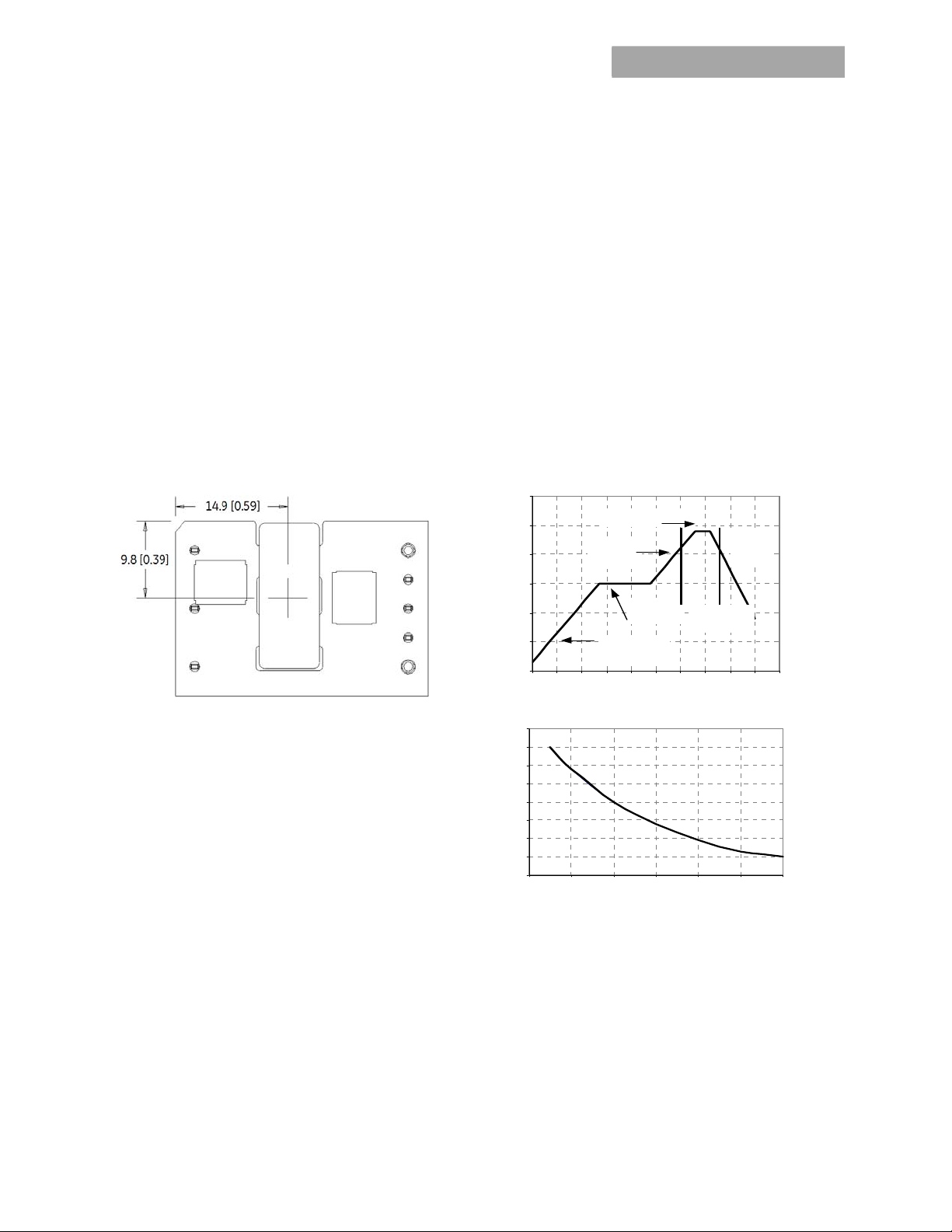
Pick and Place
The KHHD-SR series of DC-to-DC power converters use an
open-frame construction and are designed for surface mount
assembly within a fully automated manufacturing process.
The KHHD-SR series modules are designed to use the main
magnetic component surface to allow for pick and place.
Note: All dimensions in mm [in].
Figure 19. Pick and Place Location.
Z Plane Height
The ‘Z’ plane height of the pick and place location is 7.50mm
nominal with an RSS tolerance of +/-0.25 mm.
Nozzle Recommendations
The module weight has been kept to a minimum by using open
frame construction. Even so, they have a relatively large mass
when compared with conventional SMT components.
Variables such as nozzle size, tip style, vacuum pressure and
placement speed should be considered to optimize this
process.
The minimum recommended nozzle diameter for reliable
operation is 5mm. The maximum nozzle outer diameter, which
will safely fit within the allowable component spacing, is
6.5mm.
Oblong or oval nozzles up to 11 x 6 mm may also be used
within the space available.
For further information please contact your local GE Technical
Sales Representative.
Reflow Soldering Information
These power modules are large mass, low thermal
resistance devices and typically heat up slower than other
SMT components. It is recommended that the customer
review data sheets in order to customize the solder reflow
profile for each application board assembly.
The following instructions must be observed when SMT
soldering these units. Failure to observe these instructions
may result in the failure of or cause damage to the modules,
and can adversely affect long-term reliability.
There are several types of SMT reflow technologies currently
used in the industry. These surface mount power modules
can be reliably soldered using natural forced convection, IR
(radiant infrared), or a combination of convection/IR. The
recommended linear reflow profile using Sn/Pb solder is
shown in Figure 20 and 21. For reliable soldering the solder
reflow profile should be established by accurately measuring
the module’s pin connector temperatures.
300
250
200
150
10 0
REFLOW TEMP (C)
50
0
Pe ak Temp 235oC
Heat zo ne
oCs-1
max 4
Soak zone
30-240s
Pr eheat zone
oCs-1
max 4
REFLOW TIME (S)
T
205
lim
Co oling
zo ne
1- 4
above
o
C
oCs-1
Figure 20. Recommended Reflow Profile for Sn/Pb solder.
240
235
230
225
220
215
210
MAX TEMP SOLDER (C)
205
200
0 10 2030405060
TIME LIMIT (S)
Figure 21. Time Limit, T
, Curve Above 205oC Reflow.
lim
Lead Free Soldering
The –Z version SMT modules of the KHHD015A0F series are
lead-free (Pb-free) and RoHS compliant and are compatible in a
Pb-free soldering process. Failure to observe the instructions
below may result in the failure of or cause damage to the
modules and can adversely affect long-term reliability.
April 1, 2013 ©2012 General Electric Company. All rights reserved. Page 10
Page 11

GE
Data Sheet
KHHD015A0F Hammerhead™ Series; DC-DC Converter Power Modules
18-75Vdc Input; 3.3Vdc, 12A/15A Output
Surface Mount Information (continued)
Pb-free Reflow Profile
Power Systems will comply with J-STD-020 Rev. C
(Moisture/Reflow Sensitivity Classification for Nonhermetic
Solid State Surface Mount Devices) for both Pb-free solder
profiles and MSL classification procedures. This standard
provides a recommended forced-air-convection reflow profile
based on the volume and thickness of the package (table 4-2).
The suggested Pb-free solder paste is Sn/Ag/Cu (SAC). The
recommended linear reflow profile using Sn/Ag/Cu solder is
shown in Figure 22.
300
Per J-STD-020 Rev. C
250
200
150
100
Reflow Temp (°C)
50
Heating Zone
1°C/Second
Peak Temp 260°C
* Min. Time Above 235°C
15 Seconds
*Time Above 217°C
60 Seconds
Cooling
Zone
0
Figure 22. Recommended linear reflow profile using
Reflow Time (Seconds)
Sn/Ag/Cu solder.
MSL Rating
The KHHD015A0F series SMT modules have a MSL rating of 2a.
Storage and Handling
The recommended storage environment and handling
procedures for moisture-sensitive surface mount packages is
detailed in J-STD-033 Rev. A (Handling, Packing, Shipping and
Use of Moisture/Reflow Sensitive Surface Mount Devices).
Moisture barrier bags (MBB) with desiccant are required for
MSL ratings of 2 or greater. These sealed packages should not
be broken until time of use. Once the original package is
broken, the floor life of the product at conditions of
30°C and
60% relative humidity varies according to the MSL rating (see
J-STD-033A). The shelf life for dry packed SMT packages will be
a minimum of 12 months from the bag seal date, when stored
at the following conditions: < 40° C, < 90% relative humidity.
Post Solder Cleaning and Drying Considerations
Post solder cleaning is usually the final circuit-board assembly
process prior to electrical board testing. The result of
inadequate cleaning and drying can affect both the reliability
of a power module and the testability of the finished
circuit-board assembly. For guidance on appropriate soldering,
cleaning and drying procedures, refer to GE Board Mounted
Power Modules: Soldering and Cleaning Application Note
(AP01-056EPS).
April 1, 2013 ©2012 General Electric Company. All rights reserved. Page 11
Page 12
G
K
1
A
M
D
T
E
1
n
e
O
f
-
+
a
d
o
s
m
A
©
1
0
e
E
a
h
C
y
t
t
n
v
P
e
o
1
Data Sh
et
HHD0
8-75Vdc I
echanica
imensions ar
olerances: x.x
x.xx
Top
View
Side
View
5A0F H
put; 3.3V
l Outline f
in millimeter
mm 0.5 mm
mm 0.25 m
mmerh
c, 12A/15
r KHHD0
and [inches].
[x.xx in. 0.02
[x.xxx in 0.
ead™ S
Output
5A0F Surf
in.] (Unless ot
10 in.]
ries; D
ce-Moun
erwise indica
-DC Co
Module
ed)
verter
ower M
dules
Bottom
View
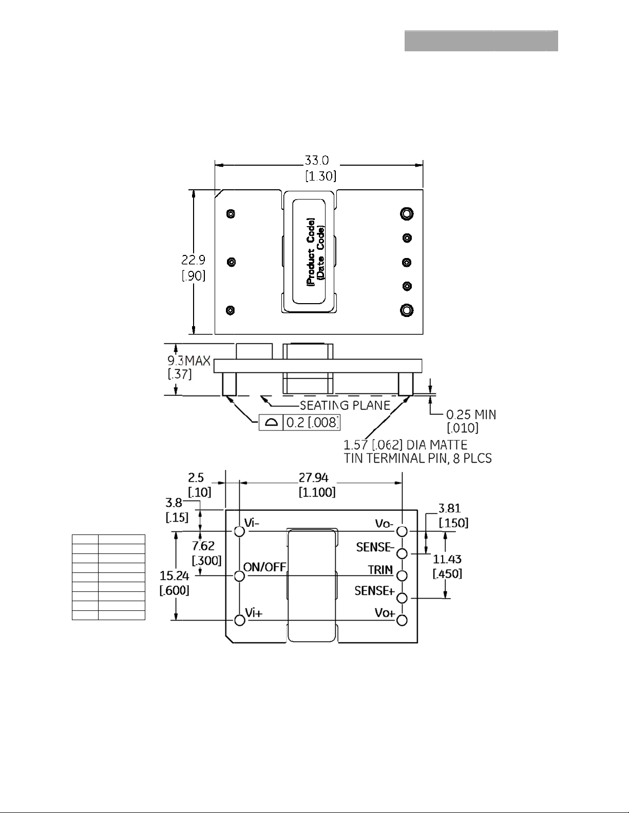
PIN FUNCTI
1 V
2 On/Of
3 V
4 V
5 Sense
6 Trim
7 Sense
8 Vo
pril 1, 2013
IN(+)
IN(-)
o(-)
(
)
(
)
(+)
N
2012 General
lectric Compan
. All rights reser
ed.
Page
2
Page 13
GE
Data Sheet
KHHD015A0F Hammerhead™ Series; DC-DC Converter Power Modules
18-75Vdc Input; 3.3Vdc, 12A/15A Output
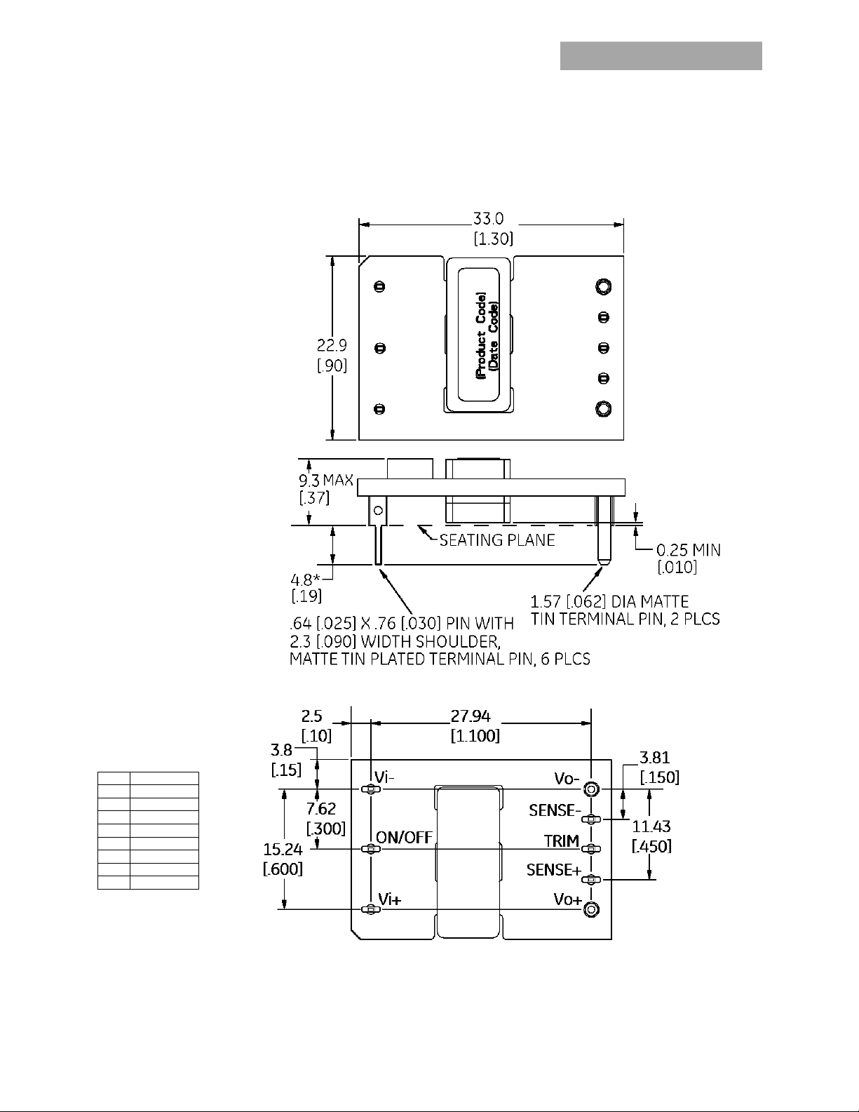
Mechanical Outline for KHHD015A0F Through Hole Module
Dimensions are in millimeters and [inches].
Tolerances: x.x mm
x.xx mm
Top
View
Side
View
0.5 mm [x.xx in. 0.02 in.] (Unless otherwise indicated)
0.25 mm [x.xxx in 0.010 in.]
* Optional PIN Lengths shown In Device Option Table
Bottom View
PIN FUNCTION
1 VIN(+)
2 On/Off
3 VIN(-)
4 Vo(-)
5 Sense(-)
6 Trim
7 Sense(+)
8 Vo(+)
April 1, 2013 ©2012 General Electric Company. All rights reserved. Page 13
Page 14

G
K
1
A
R
D
T
E
1
n
n
e
a
d
a
s
m
F
A
©
S
0
0
e
E
o
h
u
p
u
C
y
h
t
0
m
n
v
l
a
P
h
e
o
1
Data Sh
et
HHD0
8-75Vdc I
ecomme
imensions ar
olerances: x.x
x.xx
5A0F H
put; 3.3V
ded Pad L
in millimeter
mm 0.5 mm
mm 0.25 m
mmerh
c, 12A/15
yout for
and [inches].
[x.xx in. 0.02
[x.xxx in 0.
ead™ S
Output
urface M
in.] (Unless ot
10 in.]
ries; D
unt and T
erwise indica
-DC Co
rough Ho
ed)
verter
e Module
ower M
dules
Surfa
ce Mount Pad
Layout
Thro
gh-Hole Pad
or .025 x .03
For .062 d
rectangular
iameter pin,
in, use a .05
se a .076 dia
Layout
diameter pl
eter plated t
ted through
hrough hole.
ole
pril 1, 2013
2012 General
lectric Compan
. All rights reser
ed.
Page
4
Page 15
GE
Data Sheet
KHHD015A0F Hammerhead™ Series; DC-DC Converter Power Modules
18-75Vdc Input; 3.3Vdc, 12A/15A Output
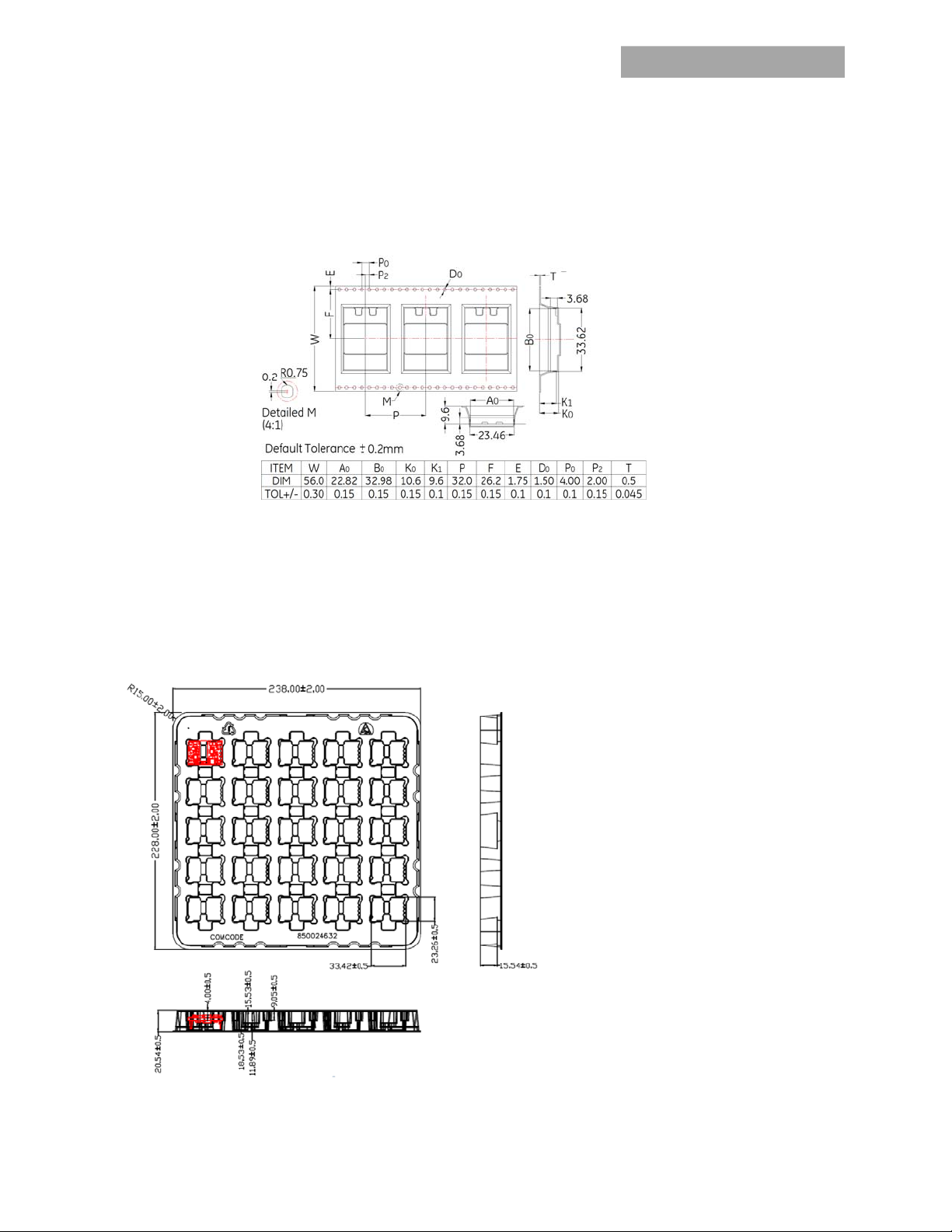
Packaging Details
The KHHD015A0F series SMT versions are supplied in tape & reel as standard. Details of tape dimensions are shown below.
Modules are shipped in quantities of 140 modules per reel.
Tape Dimensions
Dimensions are in millimeters
.
Reel Dimensions
Outside Diameter: 330mm
Inside Diameter: 178mm
Tape Width: 56mm
Tray Dimensions
The KHHD015A0F - series Through Hole versions are supplied in trays as standard. Details of tray dimensions are shown
below. Modules are shipped in quantities of 75 modules per box.
Dimensions are in millimeters.
Tolerances: x.x mm
x.xx mm
0.5 mm (unless otherwise indicated)
0.25 mm
Material PET (1mm)
Max surface
resistivity
Color Clear
Capacity 25power modules
Min order
quantity
April 1, 2013 ©2012 General Electric Company. All rights reserved. Page 15
9
-1011/PET
10
75pcs (1 box of 3 full
trays + 1 empty top
tray)
Page 16

GE
Data Sheet
KHHD015A0F Hammerhead™ Series; DC-DC Converter Power Modules
18-75Vdc Input; 3.3Vdc, 12A/15A Output
Ordering Information
Please contact your GE Sales Representative for pricing, availability and optional features.
Table 1. Device Codes
Product codes Input Voltage Output Current
KHHD015A0F41Z 24V/48V (18-75Vdc)
KHHD015A0F41-SRZ 24V/48V (18-75Vdc)
Table 2. Device Options
Output
Voltage
12A (18-36VIN)
15A (36-75VIN)
12A (18-36VIN)
15A (36-75VIN)
Remote On/Off
Logic
3.3V Negative Through hole
3.3V Negative Surface mount
Connector
Type
Comcodes
CC109172994
CC109173002
Contact Us
For more information, call us at
USA/Canada:
+1 888 546 3243, or +1 972 244 9288
Asia-Pacific:
+86.021.54279977*808
Europe, Middle-East and Africa:
+49.89.878067-280
India:
+91.80.28411633
April 1, 2013 ©2012 General Electric Company. All rights reserved. Version 1.01
www.ge.com/powerelectronics
 Loading...