

Page 1

GE
Data Sheet
JNCW016A0R Orca* Series; DC-DC Converter Power Modules
36–75 Vdc Input; 28Vdc Output; 16Adc Output
RoHS Compliant
Applications
RF Power Amplifier
Wireless Networks
Switching Networks
Options
Output OCP/OVP auto restart
Shorter pins
Unthreaded heatsink holes
Tunable Loop* for transient response optimization
Features
Compliant to RoHS II EU Directive 2011/65/EC (-Z versions)
Compliant to REACH Directive (EC) No 1907/2006
High power density: 166 W/in
Very high efficiency: >93.5% Typ at Full Load
Industry standard half-brick pin-out
Low output ripple and noise
Industry standard, DOSA compliant half-brick footprint
57.7mm x 60.7mm x 12.7mm
(2.27” x 2.39” x 0.5”)
Remote Sense
Supports repetitive loads (AC+DC) up to 2 kHz
2:1 input voltage range
Single tightly regulated output
Constant switching frequency
Constant Current Overcurrent limit
Latch after short circuit fault shutdown
Over temperature protection auto restart
Output voltage adjustment trim, 16.0V
Wide operating case temperature range (-40°C to 100°C)
CE mark meets 2006/95/EC directives
#
ANSI/UL
60950-1, 2nd Ed. Recognized, CSA† C22.2 No. 60950-
1-07 Certified, and VDE
**
ISO
9001 and ISO 14001 certified manufacturing facilities
Compliant to IPC-9592A, Category 2, Class II
3
to 35.2Vdc
dc
§
‡
0805-1 (EN60950-1, 2nd Ed.) Licensed
Description
The JNCW016A0R ORCA series of dc-dc converters are a new generation of isolated, very high efficiency DC/DC power modules
providing up to up to 16Adc output current at a nominal output voltage of 28Vdc in an industry standard, DOSA compliant halfbrick size footprint, which makes it an ideal choice for high voltage and high power applications. Threaded-through holes are
provided to allow easy mounting or addition of a heatsink for high-temperature applications. The output is fully isolated from the
input, allowing versatile polarity configurations and grounding connections. This module contains an optional new capability, the
Tunable Loop, that allows the user to optimize the dynamic response of the converter to match the load with reduced amount of
output capacitance, leading to savings on cost and PWB area.
*
Trademark of General Electric Company
#
UL is a registered trademark of Underwriters Laboratories, Inc.
†
CSA is a registered trademark of Canadian Standards Association.
‡
VDE is a trademark of Verband Deutscher Elektrotechniker e.V.
** ISO is a registered trademark of the International Organization of Standards
August 14, 2013 ©2012 General Electric Company. All rights reserved. Page 1
Page 2

GE
Data Sheet
JNCW016A0R Orca Series; DC-DC Converter Power
Modules
36–75 Vdc Input; 28.0Vdc Output; 16Adc Output
Absolute Maximum Ratings
Stresses in excess of the absolute maximum ratings can cause permanent damage to the device. These are absolute stress ratings
only, functional operation of the device is not implied at these or any other conditions in excess of those given in the operations
sections of the data sheet. Exposure to absolute maximum ratings for extended periods can adversely affect the device reliability.
Parameter Device Symbol Min Max Unit
Input Voltage
Continuous All V
Transient, operational (≤100 ms) All V
Operating Ambient Temperature All Ta
Operating Case Temperature
(See Thermal Considerations section, Figure 17)
Storage Temperature All T
I/O Isolation Voltage: Input to Case, Input to Output All
Output to Case All
All Tc -40 100 °C
IN,trans
IN
stg
-0.3 80 Vdc
-0.3 100 Vdc
-40 85 °C
-55 125 °C
1500 Vdc
500 Vdc
Electrical Specifications
Unless otherwise indicated, specifications apply over all operating input voltage, resistive load, and temperature conditions.
Parameter Device Symbol Min Typ Max Unit
Operating Input Voltage
(see Figure 12 for V
Maximum Input Current
(VIN=36V to 75V, IO=I
Inrush Transient All I2t 2 A2s
Input Reflected Ripple Current, peak-to-peak
(5Hz to 20MHz, 12μH source impedance; V
see Figure 7)
Input Ripple Rejection (120Hz) All 50 dB
when using trim-up feature)
IN MIN
) All I
O, max
=0V to 75V, IO= I
IN
Omax
;
CAUTION: This power module is not internally fused. An input line fuse must always be used.
This power module can be used in a wide variety of applications, ranging from simple standalone operation to being an integrated
part of complex power architecture. To preserve maximum flexibility, internal fusing is not included. Always use an input line fuse,
to achieve maximum safety and system protection. The safety agencies require a time-delay or fast-acting fuse with a maximum
rating of 25 A in the ungrounded input connection (see Safety Considerations section). Based on the information provided in this
data sheet on inrush energy and maximum dc input current, the same type of fuse with a lower rating can be used. Refer to the
fuse manufacturer’s data sheet for further information.
All V
All 20 mA
36 48 75 Vdc
IN
IN,max
14.0 Adc
p-p
August 14, 2013 ©2012 General Electric Company. All rights reserved. Page 2
Page 3

GE
Data Sheet
JNCW016A0R Orca Series; DC-DC Converter Power
Modules
36–75 Vdc Input; 28.0Vdc Output; 16Adc Output
Electrical Specifications (continued)
Parameter Device Symbol Min Typ Max Unit
Output Voltage Set-point
(V
IN=VIN,nom
, IO=I
O, max
, Tc =25°C)
All V
O, set
Output Voltage Set-Point Total Tolerance
(Over all operating input voltage, resistive load, and temperature
All V
O
conditions until end of life)
Output Regulation
Line (VIN=V
Load (IO=I
IN, min
O, min
to V
) All
IN, max
to I
) All
O, max
Temperature (Tc = -40ºC to +100ºC) All
Output Ripple and Noise on nominal output
(VIN=V
IN, nom
and IO=I
O, min
to I
)
O, max
RMS (5Hz to 20MHz bandwidth) All
Peak-to-Peak (5Hz to 20MHz bandwidth) All
,
All,
except -T
-T C
All I
All I
C
O,
O,max
o
O, lim
O, sc
O
O
All η 93.0 93.5
sw
External Capacitance
Without the Tunable Loop1 -T C
With the Tunable Loop
2
Output Power (Vo=28V to 35.2V) All P
Output Current All I
Output Current Limit Inception (Constant current until Vo<V
trimMIN
duration <4s)
Output Short Circuit Current (VO≤ 0.25Vdc)
Hiccup mode 5 A
Efficiency
V
IN=VIN, nom
, Tc=25°C IO=I
O, max , VO
= V
O,set
Switching Frequency f
Dynamic Load Response
(Io/t=1A/10s; Vin=Vin,nom; Tc=25°C; Tested with a 470 μF
aluminum and a 10 µF ceramic capacitor across the load.)
Load Change from Io= 50% to 75% of Io,max: Peak Deviation
Settling Time (Vo<10% peak deviation)
Load Change from Io= 25% to 50% of Io,max: Peak Deviation
Settling Time (Vo<10% peak deviation)
(Io/t=2A/10s; Vin=Vin,nom; Tc=25°C; Tested with a 880 μF
aluminum and a 10 µF ceramic capacitor across the load.)
Load Change from Io= 0% to 75% of Io,max: Peak Deviation
Settling Time (Vo<10% peak deviation)
Load Change from Io= 75% to 0% of Io,max: Peak Deviation
Settling Time (Vo<10% peak deviation)
1
Use a minimum 2 x 220uF output capacitor. Recommended capacitor is Nichicon PM series, 220uF/35V. If the ambient temperature at module
startup is between 0
startup below -20
2
External capacitors may require using the new Tunable Loop feature to ensure that the module is stable as well as getting the best transient
response. See the Tunable Loop section for details.
O
C and -10OC, use a minimum 3 x 220uF capacitors, and between -10OC and -20OC, use a minimum 4 x 220uF capacitors. For
O
C, use 440uF minimum polymer capacitors.
All
All
V
pk
t
s
V
pk
t
s
V
pk
t
s
V
pk
t
s
27.5 28 28.5 V
27.0
0.1 0.2 %V
0.1 0.2 %V
45 55 mV
80 200 mV
440 6500 μF
440 470 μF
440 10,000 μF
0 16.0 Adc
17.5
60 Apk
175
1
1.0
1
1.0
2
1.0
2
1.0
29.0 V
0.02 %/°C
450 W
21.0 Adc
%V
%V
%V
%V
rms
%
kHz
ms
ms
ms
ms
dc
dc
o,set
o,set
rms
pk-pk
O, set
O, set
O, set
O, set
Isolation Specifications
Parameter Symbol Min Typ Max Unit
Isolation Capacitance C
Isolation Resistance R
iso
iso
10
15
August 14, 2013 ©2012 General Electric Company. All rights reserved. Page 3
nF
MΩ
Page 4

GE
y
Data Sheet
JNCW016A0R Orca Series; DC-DC Converter Power
Modules
36–75 Vdc Input; 28.0Vdc Output; 16Adc Output
General Specifications
Parameter Device Symbol Min Typ Max Unit
Calculated Reliability based upon Telcordia SR-332 Issue 3:
Method
I Case 3 (I
=80%I
O
, TA=40°C, airflow = 200 lfm, 90%
O, max
All
confidence)
Weight All
FIT 214.5 10
MTBF 4,661,316 Hours
76.4
2.69 oz.
9
/Hours
g
Feature Specifications
Unless otherwise indicated, specifications apply over all operating input voltage, resistive load, and temperature conditions. See
Feature Descriptions for additional information.
Parameter Device Symbol Min Typ Max Unit
Remote On/Off Signal Interface
(VIN=V
Signal referenced to V
Negative Logic: device code suffix “1”
Logic Low = module On, Logic High = module Off
Positive Logic: No device code suffix required
Logic Low = module Off, Logic High = module On
Turn-On Delay and Rise Times
(Vin=V
Case 1: T
with Remote On/Off set to ON,
Case 2: T
Remote On/Off from Off to On with V
one second.
T
Output Voltage Overshoot
(IO=80% of I
Output Voltage Adjustment
(See Feature Descriptions):
Output Voltage Remote-sense Range
(onl
Output Voltage Set-point Adjustment Range (trim) All V
Output Overvoltage Protection
Over Temperature Protection All T
(See Feature Descriptions, Figure 17)
Input Under Voltage Lockout V
Input Over voltage Lockout V
to V
IN, min
; open collector or equivalent,
IN, max
terminal)
IN-
Logic Low - Remote On/Off Current All I
Logic Low - On/Off Voltage All V
Logic High Voltage – (Typ = Open Collector) All V
Logic High maximum allowable leakage current All I
, IO=I
in,nom
delay
delay
= time for VO to rise from 10% of V
rise
for No Trim or Trim down application )
, 25C)
O, max
= Time until VO = 10% of V
= Time until VO = 10% of V
, TA=25°C)
O, max
from application of Vin
O,set
from application of
O,set
already applied for at least
in
to 90% of V
O,set
. All T
O,set
All T
All T
All V
All V
Turn-on Threshold All
Turn-off Threshold All
Hysteresis All
Turn-on Threshold All
Turn-off Threshold All
Hysteresis All
on/off
on/off
on/off
on/off
120 ms
delay
delay
rise
0
sense
16.0 --- 35.2 Vdc
trim
O, limit
ref
__
37
5 V
20 ms
30
__
110
1.0 mA
1.2 Vdc
dc
50 μA
3 % V
2 %V
ms
O, set
o,nom
39 Vdc
°C
IN, UVLO
IN, OVLO
35 36 Vdc
31 32 Vdc
3 Vdc
79.5 81 V
81 83
Vdc
dc
--- 3 --- Vdc
August 14, 2013 ©2012 General Electric Company. All rights reserved. Page 4
Page 5
GE
O
/Off
O
G
O
O
G
O
G
O
O
G
Data Sheet
JNCW016A0R Orca Series; DC-DC Converter Power Modules
36–75 Vdc Input; 28.0Vdc Output; 16Adc Output
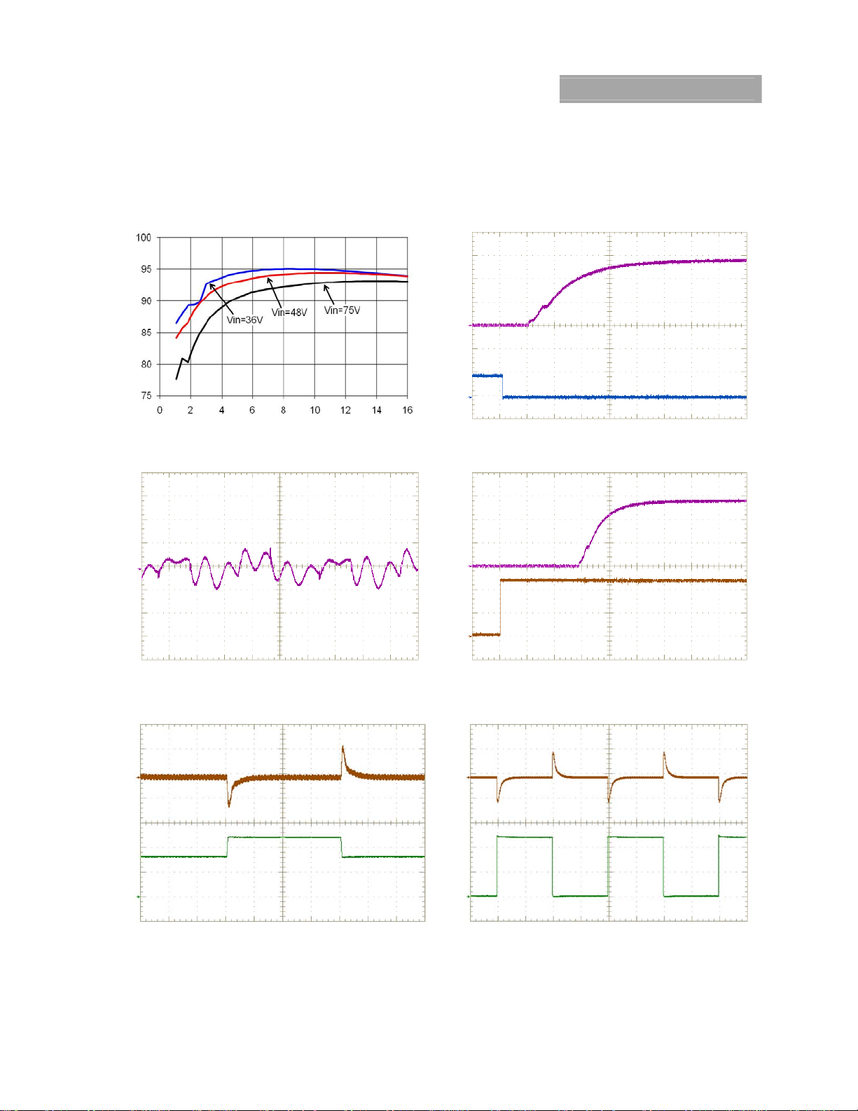
Characteristic Curves
The following figures provide typical characteristics for the JNCW016A0R (28V, 16A) at 25ºC. The figures are identical for either
positive or negative Remote On/Off logic.
E
LTA
(V) (10V/div)
O
UTPUTV
EFFICIENCY (%)
OUTPUT CURRENT, Io (A) TIME, t (20ms/div)
Figure 1. Converter Efficiency versus Output Current.
(V) (50mV/div)
O
V
OUTPUT VOLTAGE
TIME, t (1s/div)
Figure 2. Typical Output Ripple and Noise at Room
= I
; C
Temperature and 48Vin; I
o
o,max
= 440µF.
o,ext
E
LTA
V
(V) (5V/div) V
n
ON/OFF
V
Figure 4. Typical Start-Up Using negative Remote On/Off;
= 440µF.
C
o,ext
E
LTA
(V) (10V/div)
O
UTPUT V
E
LTA
(V) (20V/div) V
in
INPUT V
V
Figure 5. Typical Start-Up
step; C
= 470µF.
o,ext
TIME, t (40ms/div)
from VIN, on/off enabled prior to V
IN
(V) (500mV/div)
(V) (200mV/div)
O
(A) (5A/div) V
O
I
OUTPUT CURRENT OUTPUT VOLTAGE
TIME, t (1ms/div)
Figure 3. Dynamic Load Change Transient Response from
50% to 75% to 50% of Full Load at Room Temperature and
48 Vin; 0.1A/uS, C
August 14, 2013 ©2012 General Electric Company. All rights reserved. Page 5
= 470µF.
o,ext
O
(A) (5A/div) V
O
I
OUTPUT CURRENT OUTPUT VOLTAGE
TIME, t (2ms/div)
Figure 6. Dynamic Load Change Transient Response from 0
% to 75% to 0% of Full Load at Room Temperature and 48
Vin; 2.0A/uS, C
= 880µF.
o,ext
Page 6

GE
Data Sheet
JNCW016A0R Orca Series; DC-DC Converter Power
36–75 Vdc Input; 28.0Vdc Output; 16Adc Output
Test Configurations
Note: Measure the input reflected-ripple current with a simulated
source inductance (LTEST) of 12 µH. Capacitor CS offsets possible
battery impedance. Measure the current, as shown above.
Figure 7. Input Reflected Ripple Current Test Setup.
Note: Use a Cout (470 µF Low ESR aluminum or tantalum capacitor
typical), a 0.1 µF ceramic capacitor and a 10 µF ceramic capacitor,
and Scope measurement should be made using a BNC socket.
Position the load between 51 mm and 76 mm (2 in. and 3 in.) from
the module.
Figure 8. Output Ripple and Noise Test Setup.
Note: All measurements are taken at the module terminals. When
socketing, place Kelvin connections at module terminals to avoid
measurement errors due to socket contact resistance.
Figure 9. Output Voltage and Efficiency Test Setup.
Design Considerations
Input Source Impedance
The power module should be connected to a low
ac-impedance source. A highly inductive source impedance
can affect the stability of the power module. For the test
configuration in Figure 7, a 470μF Low ESR aluminum
capacitor, C
ensure the stability of the unit. Consult the factory for further
application guidelines.
, mounted close to the power module helps
IN
Output Capacitance
The JNCW016A0R power module requires a minimum
output capacitance of 440µF low ESR capacitor, C
ensure stable operation over the full range of load and line
conditions, see Figure 8. If the ambient temperature at
module startup is between 0
use at least 660uF aluminum or 440uF polymer capacitors;
and if the ambient temperature at module startup is
between -10
880uF aluminum or 440uF polymer capacitors. If the
ambient temperature at module startup is below -20
required to use only 440uF polymer capacitors. Use of
polymer capacitors can be avoided by suitable warmup
time, when starting from -40
determining the acceptable values of output capacitance
and ESR is complex and is load-dependent.
O
C and -20 OC, it is required to use at least
Safety Considerations
For safety-agency approval of the system in which the
power module is used, the power module must be installed
in compliance with the spacing and separation
requirements of the end-use safety agency standard, i.e., UL
60950-1, 2nd Ed., CSA No. 60950-1 2
EN60950-1, 2nd Ed.
For end products connected to –48V dc, or –60Vdc nominal
DC MAINS (i.e. central office dc battery plant), no further fault
testing is required. *Note: -60V dc nominal battery plants
are not available in the U.S. or Canada.
For all input voltages, other than DC MAINS, where the input
voltage is less than 60V dc, if the input meets all of the
requirements for SELV, then:
The output may be considered SELV. Output voltages
will remain within SELV limits even with internallygenerated non-SELV voltages. Single component failure
and fault tests were performed in the power converters.
One pole of the input and one pole of the output are to
be grounded, or both circuits are to be kept floating, to
maintain the output voltage to ground voltage within
ELV or SELV limits. However, SELV will not be
maintained if V
simultaneously.
Modules
O
C and -10 OC, it is required to
O
C. In general, the process of
nd
Ed., and VDE0805-1
(+) and VO(+) are grounded
I
out
to
O
C, it is
August 14, 2013 ©2012 General Electric Company. All rights reserved. Page 6
Page 7
GE
Data Sheet
JNCW016A0R Orca Series; DC-DC Converter Power
36–75 Vdc Input; 28.0Vdc Output; 16Adc Output
Safety Considerations (continued)
For all input sources, other than DC MAINS, where the input
voltage is between 60 and 75V dc (Classified as TNV-2 in
Europe), the following must be meet, if the converter’s
output is to be evaluated for SELV:
The input source is to be provided with reinforced
insulation from any hazardous voltage, including the ac
mains.
One Vi pin and one Vo pin are to be reliably earthed, or
both the input and output pins are to be kept floating.
Another SELV reliability test is conducted on the whole
system, as required by the safety agencies, on the
combination of supply source and the subject module
to verify that under a single fault, hazardous voltages
do not appear at the module’s output.
All flammable materials used in the manufacturing of these
modules are rated 94V-0, or tested to the UL60950 A.2 for
reduced thickness.
The input to these units is to be provided with a maximum
25 A fast-acting or time-delay fuse in the ungrounded input
connection.
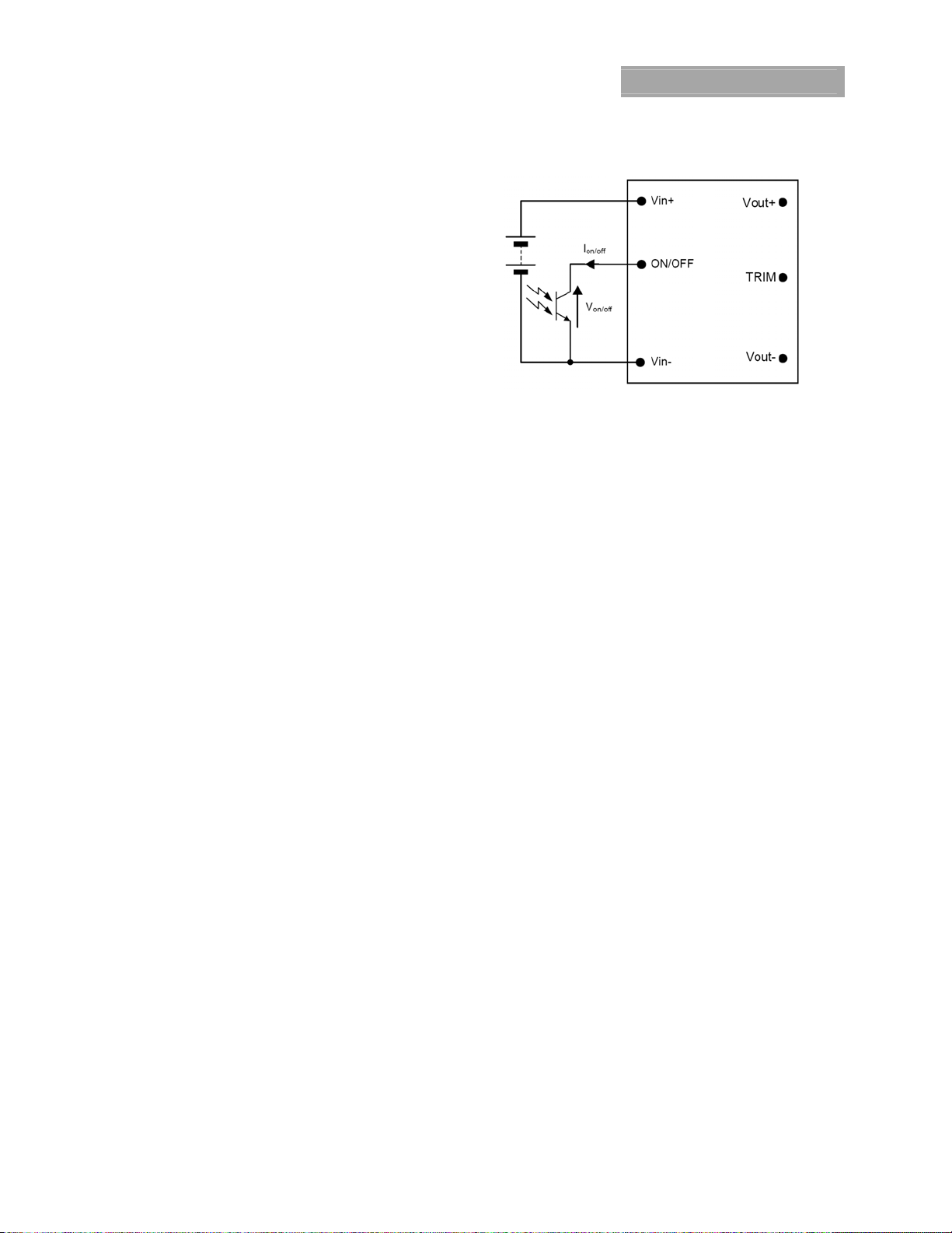
Feature Description
Remote On/Off
Two remote on/off options are available. Positive logic turns
the module on during a logic high voltage on the ON/OFF
pin, and off during a logic low. Negative logic remote On/Off,
device code suffix “1”, turns the module off during a logic
high and on during a logic low.
To turn the power module on and off, the user must supply a
switch (open collector or equivalent) to control the voltage
) between the ON/OFF terminal and the VIN(-) terminal
(V
on/off
(see Figure 10). Logic low is 0V ≤ V
during a logic low is 1mA, the switch should be
I
on/off
maintain a logic low level whilst sinking this current.
During a logic high, the typical maximum V
by the module is 5V, and the maximum allowable leakage
current at V
If not using the remote on/off feature:
For positive logic, leave the ON/OFF pin open.
For negative logic, short the ON/OFF pin to V
= 5V is 50μA.
on/off
≤ 1.2V. The maximum
on/off
generated
on/off
(-).
IN
Figure 10. Circuit configuration for using Remote On/Off
Implementation.
Overcurrent Protection
To provide protection in a fault output overload condition,
the module is equipped with internal current limiting
protection circuitry, and can endure continuous overcurrent
by providing constant current output, for up to 4 seconds, as
long as the output voltage is greater than V
resistance is to low to support V
condition or a short circuit load condition exists, the module
will shutdown immediately.
A latching shutdown option is standard. Following
shutdown, the module will remain off until the module is
reset by either cycling the input power or by toggling the
on/off pin for one second.
An auto-restart option (4) is also available in a case where
an auto recovery is required. If overcurrent greater than 19A
persists for few milli-seconds, the module will shut down
and auto restart until the fault condition is corrected. If the
output overload condition still exists when the module
restarts, it will shut down again. This operation will continue
indefinitely, until the overcurrent condition is corrected.
Over Voltage Protection
The output overvoltage protection consists of circuitry that
monitors the voltage on the output terminals. If the voltage
on the output terminals exceeds the over voltage protection
threshold, then the module will shutdown and latch off. The
overvoltage latch is reset by either cycling the input power
for one second or by toggling the on/off signal for one
second. The protection mechanism is such that the unit can
continue in this condition until the fault is cleared.
An auto-restart option (4) is also available in a case where
an auto recovery is required.
Remote sense
Remote sense minimizes the effects of distribution losses by
regulating the voltage at the remote-sense connections (see
Figure 11). For No Trim or Trim down application, the voltage
between the remote-sense pins and the output terminals
must not exceed the output voltage sense range given in
the Feature Specifications table i.e.:
(+)–Vo(-)] – [SENSE(+) – SENSE(-)] 2% of V
[V
o
Modules
in an overcurrent
trimMIN
trimMIN
o,nom
. If the load
August 14, 2013 ©2012 General Electric Company. All rights reserved. Page 7
Page 8

GE
Data Sheet
JNCW016A0R Orca Series; DC-DC Converter Power
36–75 Vdc Input; 28.0Vdc Output; 16Adc Output
Feature Description (continued)
The voltage between the Vo(+) and Vo(-) terminals must not
exceed the minimum output overvoltage shut-down value
indicated in the Feature Specifications table. This limit
includes any increase in voltage due to remote-sense
compensation and output voltage set-point adjustment
(trim). See Figure 11. If not using the remote-sense feature to
regulate the output at the point of load, then connect
SENSE(+) to V
Although the output voltage can be increased by both the
remote sense and by the trim, the maximum increase for
the output voltage is not the sum of both. The maximum
increase is the larger of either the remote sense or the trim.
The amount of power delivered by the module is defined as
the voltage at the output terminals multiplied by the output
current. When using remote sense and trim: the output
voltage of the module can be increased, which at the same
output current would increase the power output of the
module. Care should be taken to ensure that the maximum
output power of the module remains at or below the
maximum rated power.
(+) and SENSE(-) to Vo(-) at the module.
o
Trim Down – Decrease Output Voltage
With an external resistor (R
SENSE(-) pins, the output voltage set point (V
(see Figure 13). The following equation determines the
required external-resistor value to obtain a percentage
output voltage change of %.
For output voltages:
Without –T Option
100
kR downadj 2
_
%
Where,
,
= Desired output voltage set point (V).
V
desired
VV
,
nomo
V
Modules
adj_down
V
= 28V
O,nom
desirednomo
100%
) between the TRIM and
) decreases
o,adj
With –T Option
1000
kR
downadj 11
_
%
Figure 11. Effective Circuit Configuration for SingleModule Remote-Sense Operation Output Voltage.
Output Voltage Programming
Trimming allows the user to increase or decrease the output
voltage set point of a module. Trimming down is
accomplished by connecting an external resistor between
the TRIM pin and the SENSE(-) pin. Trimming up is
accomplished by connecting external resistor between the
SENSE(+) pin and TRIM pin. The trim resistor should be
positioned close to the module. Certain restrictions apply to
the input voltage lower limit when trimming the output
voltage to the maximum.
35
30
25
Vout (V)
20
15
35 40 45 50 55 60 65 70 75
Figure 12. Output Voltage Trim Limits vs. Input Voltage.
See Figure 12 for the allowed input to output range when
using trim. If not using the trim down feature, leave the TRIM
pin open.
Upper Trim Limit
Lower Trim Limit
Vin (V)
Figure 13. Circuit Configuration to Decrease Output
Voltage.
Trim Up – Increase Output Voltage
With an external resistor (Radj_up) connected between the
SENSE(+) and TRIM pins
increases (see Figure 14).
The following equation determines the required externalresistor value to obtain a percentage output voltage change
of %.
For output voltages: V
Without –T Option
upadj
_
k
R
With –T Option
kR upadj 12.15
_
Where,
= Desired output voltage set point (V).
V
desired
The voltage between the Vo(+) and Vo(-) terminals must not
exceed the minimum output overvoltage shut-down value
indicated in the Feature Specifications table.
, the output voltage set point (V
= 28V
O,nom
%)100(
V
27122
%
,
nomo
V
nomO
,
VV
,
nomodesired
%225.1
100%
)
o,adj
%)2(100(
%
August 14, 2013 ©2012 General Electric Company. All rights reserved. Page 8
Page 9

GE
Data Sheet
JNCW016A0R Orca Series; DC-DC Converter Power Modules
36–75 Vdc Input; 28.0Vdc Output; 16Adc Output
Feature Description (continued)
Figure 14. Circuit Configuration to Increase Output
Voltage.
This limit includes any increase in voltage due to remotesense compensation and output voltage set-point
adjustment (trim). See Figure 11.
Although the output voltage can be increased by both the
remote sense and by the trim, the maximum increase for
the output voltage is not the sum of both.
The maximum increase is the larger of either the remote
sense or the trim. The amount of power delivered by the
module is defined as the voltage at the output terminals
multiplied by the output current. When using remote sense
and trim, the output voltage of the module can be
increased, which the same output current would increase
the power output of the module. Care should be taken to
ensure that the maximum output power of the module
remains at or below the maximum rated power.
Examples:
To trim down the output of a nominal 28V module, without –
T option, to 16.8V
8.1628
%
28
100
downadj
_
40
To trim up the output of a nominal 28V module, without –T
option, to 30.8V
%
28
_ upadj
R
R
Active Voltage Programming
For both the JNCW016A0Rx and JNCW016A0Rx-T, a DigitalAnalog converter (DAC), capable of both sourcing and
sinking current, can be used to actively set the output
voltage, as shown in Figure 15. The value of R
dependent on the voltage step and range of the DAC and
the desired values for trim-up and trim-down
August 14, 2013 ©2012 General Electric Company. All rights reserved. Page 9
adj_up
= 239kΩ
kR
5.02
288.30
)10100(28
10225.1
%40100
%0.10100
)102(100(
will be
G
∆%.
Please
10
contact your GE technical representative to obtain more
details on the selection for this resistor.
Figure 15. Circuit Configuration to Actively Adjust the
Output Voltage.
AC+DC Load Capability
The JRCW016A0Rx is compatible with load profiles as shown
in Figure 16.
Figure 16. AC-DC Load Profile
The output voltage peak deviation shall not exceed the peak
values listed in the Electrical Specifications Table.
Tunable Loop
The JNCW016A0Rx-T modules have a new feature that
optimizes transient response of the module called Tunable
Loop. External capacitors are usually added to the output of
the module for two reasons: to reduce output ripple and
noise and to reduce output voltage deviations from the
steady-state value in the presence of dynamic load current
changes.
Page 10

GE
Data Sheet
JNCW016A0R Orca Series; DC-DC Converter Power Modules
36–75 Vdc Input; 28.0Vdc Output; 16Adc Output
Feature Description (continued)
Adding external capacitance however affects the voltage
control loop of the module, typically causing the loop to slow
down with sluggish response. Larger values of external
capacitance could also cause the module to become
unstable.
The Tunable Loop allows the user to externally adjust the
voltage control loop to match the filter network connected
to the output of the module. The Tunable Loop is
implemented by connecting a series R-C between the
SENSE(+) and TRIM pins of the module, as shown in Fig. 17.
This R-C allows the user to externally adjust the voltage loop
feedback compensation of the module.
Figure 17. Circuit diagram showing connection of R
and C
Table 1 shows the recommended values of R
to tune the control loop of the module.
TUNE
TUNE
and C
for different values of ceramic output capacitors up to
8000uF that might be needed for an application to meet
output ripple and noise requirements.
Table 1. General recommended values of of R
C
for V
TUNE
=28V and various external ceramic capacitor
out
TUNE
combinations.
C
(µF) 1100 2200 4400 6600 8800
out
ESR (mΩ) 60 30 15 10 7.5
R
C
TUNE
TUNE
* * * * *
* * * * *
* contact GE technical support
Please contact your GE technical representative to obtain
more details of this feature as well as for guidelines on how
to select the right value of external R-C to tune the module
for best transient performance and stable operation for
other output capacitance values.
Over Temperature Protection
The JNCW016A0R module provides a non-latching over
temperature protection. A temperature sensor monitors the
operating temperature of the converter. If the reference
temperature, T
115 ºC (typical), the converter will shut down and disable the
output. When the base plate temperature has decreased by
approximately 20 ºC the converter will automatically restart.
The module can be restarted by cycling the dc input power
for at least one second or by toggling the remote on/off
signal for at least one second.
, (see Figure 17) exceeds a threshold of
REF 1
TUNE
and
TUNE
Thermal Considerations
The power modules operate in a variety of thermal
environments; however, sufficient cooling should be
provided to help ensure reliable operation of the unit. Heatdissipating components inside the unit are thermally
coupled to the case. Heat is removed by conduction,
convection, and radiation to the surrounding environment.
Proper cooling can be verified by measuring the case
temperature. Peak temperature (TREF) occurs at the position
indicated in Figure 18.
Considerations include ambient temperature, airflow,
module power dissipation, and the need for increased
reliability. A reduction in the operating temperature of the
module will result in an increase in reliability.
The thermal data presented here is based on physical
measurements taken in a wind tunnel, using automated
thermo-couple instrumentation to monitor key component
temperatures: FETs, diodes, control ICs, magnetic cores,
ceramic capacitors, opto-isolators, and module pwb
conductors, while controlling the ambient airflow rate and
temperature. For a given airflow and ambient temperature,
the module output power is increased, until one (or more) of
the components reaches its maximum derated operating
temperature, as defined in IPC-9592. This procedure is then
repeated for a different airflow or ambient temperature until
a family of module output derating curves is obtained.
Heat-dissipating components inside the unit are thermally
coupled to the case. Heat is removed by conduction,
convection, and radiation to the surrounding environment.
For reliable operation this temperature should not
or T
exceed 100ºC at either T
REF 1
for applications using
REF 2
forced convection airflow or cold plate applications. The
output power of the module should not exceed the rated
power for the module as listed in the ordering Information
table. Although the maximum T
temperature of the power
REF
modules is discussed above, you can limit this temperature
to a lower value for extremely high reliability.
August 14, 2013 ©2012 General Electric Company. All rights reserved. Page 10
Page 11

GE
Data Sheet
JNCW016A0R Orca Series; DC-DC Converter Power
36–75 Vdc Input; 28.0Vdc Output; 16Adc Output
Thermal Considerations (continued)
Figure 18.
(top view).
Thermal Derating
Thermal derating is presented for two different applications:
1) Figure 19, the JNCW016A0R module is thermally coupled
to a cold plate inside a sealed clamshell chassis, without any
internal air circulation; and 2) Figure 20 , 21 and 22, the
JNCW016A0R module is mounted in a traditional open
chassis or cards with forced air flow. In application 1, the
module is cooled entirely by conduction of heat from the
module primarily through the top surface to a cold plate,
with some conduction through the module’s pins to the
power layers in the system board. For application 2, the
module is cooled by heat removal into a forced airflow that
passes through the interior of the module and over the top
base plate and/or attached heatsink.
Case (T
) Temperature Measurement Location
REF
(A)
O
Output Current, I
Figure 20. Derating Output Current vs. local Ambient
temperature and Airflow, No Heatsink, Vin=48V, airflow
from Vi(-) to Vi(+).
(A)
O
Output Current, I
Figure 21. Derating Output Current vs. local Ambient
temperature and Airflow, 0.5” Heatsink, Vin=48V, airflow
from Vi(-) to Vi(+).
Modules
Ambient Temperature, TA (oC)
Ambient Temperature, TA (oC)
(A)
O
(A)
O
Output Current, I
Output Current, I
Cold plate (inside surface) temperature
Figure 19. Output Power Derating for JNCW016A0R in
Conduction cooling (cold plate) applications; T
adjacent to module; V
August 14, 2013 ©2012 General Electric Company. All rights reserved. Page 11
IN
= V
IN,NOM
(ºC)
<70ºC
a
Ambient Temperature, TA (oC)
Figure 22. Derating Output Current vs. local Ambient
temperature and Airflow, 1.0” Heatsink, Vin=48V, airflow
from Vi(-) to Vi(+).
Page 12

GE
Data Sheet
JNCW016A0R Orca Series; DC-DC Converter Power
36–75 Vdc Input; 28.0Vdc Output; 16Adc Output
Layout Considerations
The JNCW016A0R power module series are constructed
using a single PWB with integral base plate; as such,
component clearance between the bottom of the power
module and the mounting (Host) board is limited. Avoid
placing copper areas on the outer layer directly underneath
the power module.
Post Solder Cleaning and Drying Considerations
Post solder cleaning is usually the final circuit-board
assembly process prior to electrical board testing. The result
of inadequate cleaning and drying can affect both the
reliability of a power module and the testability of the
finished circuit-board assembly. For guidance on
appropriate soldering, cleaning and drying procedures, refer
to GE Board Mounted Power Modules: Soldering and
Cleaning Application Note.
Through-Hole Lead-Free Soldering
Information
The RoHS-compliant through-hole products use the SAC
(Sn/Ag/Cu) Pb-free solder and RoHS-compliant components.
They are designed to be processed through single or dual
wave soldering machines. The pins have an RoHScompliant finish that is compatible with both Pb and Pb-free
wave soldering processes. A maximum preheat rate of 3C/s
is suggested. The wave preheat process should be such
that the temperature of the power module board is kept
below 210C. For Pb solder, the recommended pot
temperature is 260C, while the Pb-free solder pot is 270C
max. The JNCW016A0R cannot be processed with pastethrough-hole Pb or Pb-free reflow process. If additional
information is needed, please consult with your GE
representative for more details.
Modules
August 14, 2013 ©2012 General Electric Company. All rights reserved. Page 12
Page 13

GE
Data Sheet
JNCW016A0R Orca Series; DC-DC Converter Power
36–75 Vdc Input; 28.0Vdc Output; 16Adc Output
Mechanical Outline for Through-Hole Module
Dimensions are in millimeters and [inches].
Tolerances: x.x mm 0.5 mm [x.xx in. 0.02 in.] (Unless otherwise indicated)
x.xx mm 0.25 mm [x.xxx in 0.010 in.]
Pin Description
1 Vin (+)
2 On/Off
3 Baseplate
4 Vin (–)
5 Vout (–)
6 Sense (-)
7 Trim
8 Sense (+)
9 Vout (+)
TOP VIEW*
SIDE VIEW**
BOTTOM VIEW
*Top side label includes GE name, product designation, and data code.
Modules
August 14, 2013 ©2012 General Electric Company. All rights reserved. Page 13
Page 14

GE
Data Sheet
JNCW016A0R Orca Series; DC-DC Converter Power
36–75 Vdc Input; 28.0Vdc Output; 16Adc Output
Recommended Pad Layout for Through Hole Module
Dimensions are in millimeters and [inches].
Tolerances: x.x mm 0.5 mm [x.xx in. 0.02 in. ] (Unless otherwise indicated)
x.xx mm 0.25 mm [x.xxx in 0.010 in. ]
Modules
August 14, 2013 ©2012 General Electric Company. All rights reserved. Page 14
Page 15

GE
Data Sheet
JNCW016A0R Orca Series; DC-DC Converter Power
Modules
36–75 Vdc Input; 28.0Vdc Output; 16Adc Output
Ordering Information
Please contact your GE Sales Representative for pricing, availability and optional features.
Table 2. Device Code
Input Voltage
48V (36-75Vdc) 28V 16A 93.5% Through hole JNCW016A0R41Z 150030776
48V (36-75Vdc) 28V 16A 93.5% Through hole JNCW016A0R41-18Z 150030782
Table 3. Device Options
Output
Voltage
Output
Current
Efficiency
Connector
Type
Product codes Comcodes
Contact Us
For more information, call us at
USA/Canada:
+1 888 546 3243, or +1 972 244 9288
Asia-Pacific:
+86.021.54279977*808
Europe, Middle-East and Africa:
+49.89.878067-280
India:
+91.80.28411633
August 14, 2013 ©2012 General Electric Company. All rights reserved. Version 1.1
www.ge.com/powerelectronics
 Loading...