

Page 1
Data Sheet
June 26, 2009
HW006/010/012 Series Power Modules; dc-dc Converters
36-75 Vdc Input; 1.2 Vdc to 5 Vdc Output; 6.6A to 12A
RoHS Compliant
Applications
n
Distributed Power Architectures
n
Wireless Networks
n
Access and Optical Network Equipment
n
Enterprise Networks
n
Latest generation IC’s (DSP, FPGA, ASIC) and Micropro-
cessor-powered applications.
Options
n
Remote On/Off negative logic
n
Surface-mount package (–S Suffix)
n
Basic Insulation (–B Suffix)
Features
n
Compatible with RoHS EU Directive 200295/EC (-Z Ver-
sions)
n
Compatible in RoHS EU Directive 200295/EC with lead
solder exemption (non -Z versions)
n
Delivers up to 12A output current
n
High efficiency: 90% at 3.3V full load (VIN = 48V)
n
Small size and low profile:
47.2 mm x 29.5 mm x 8.50 mm
(1.86 in x 1.16 in x 0.335 in)
n
Low output ripple and noise
n
Exceptional thermal performance
n
High reliability: MTBF > 4.5M hours at 25 °C
n
Remote On/Off positive logic (primary referenced)
n
Constant switching frequency (285 KHz typical)
n
Output overvoltage and overcurrent protection
n
Overtemperature protection
n
Input undervoltage lockout
n
Adjustable output voltage (± 10%)
n
Surface mount or through-hole package
n
Meets the voltage and current requirements for
ETSI 300-132-2 and complies with and is approved for
Basic Insulation rating per IEC60950 3
n
UL* 60950 Recognized, CSA† C22.2 No. 60950-00 Certi-
fied, and VDE
n
CE mark meets 73/23/EEC and 93/68/EEC directives
n
ISO** 9001 and ISO14001 certified manufacturing facili-
‡
0805 (IEC60950, 3rd edition) Licensed
ties
rd
(-B version only)
§
Description
The HW series power modules are isolated dc-dc converters that can deliver up to 12A of output current and provide a precisely
regulated output voltage over a wide range of input voltages (VI = 36 V to 75 Vdc for HW modules). The modules achieve full load
efficiency of 90% at 3.3 V output voltage. The open frame modules, available in both surface-mount and through-hole packaging,
enable designers to develop cost- and space-efficient solutions. Standard features include remote On/Off, output voltage adjustment, overvoltage, overcurrent and overtemperature protection.
* UL is a registered trademark of Underwriters Laboratories, Inc.
† CSA is a registered trademark of Canadian Standards Association.
‡ VDE is a trademark of Verband Deutscher Elektrotechniker e.V.
§ This product is intended for integration into end-use equipment. All the required procedures for CE marking of end-use equipment should be followed. (The CE mark is placed on selected products.)
** ISO is a registered trademark of the Internation Organization of Standards
Document No: ADS02-006EPS ver.1.4
PDF Name: fds03-0031.pdf
Page 2
Data Sheet
June 26, 2009
HW006/010/012 Series Power Modules; dc-dc Converters
36-75 Vdc Input; 1.2 Vdc to 5 Vdc Output; 6.6A to 12A
Absolute Maximum Ratings
Stresses in excess of the absolute maximum ratings can cause permanent damage to the device. These are absolute stress
ratings only, functional operation of the device is not implied at these or any other conditions in excess of those given in the
operations sections of the data sheet. Exposure to absolute maximum ratings for extended periods can adversely affect the
device reliabiltiy.
Parameter Device Symbol Min Max Unit
Input Voltage:Continuous
Transient (100ms)
Operating Ambient Temperature
(See Thermal Considerations section)
Storage Temperature All Tstg –55 125 °C
HW
HW
All TA –40 85 °C
VI
VI, trans
–0.3
—
80
100
Vdc
Vdc
Electrical Specifications
Unless otherwise indicated, specifications apply over all operating input voltage, resistive load, and temperature conditions.
Parameter Device Symbol Min Typ Max Unit
Operating Input Voltage HW VIN 36 48 75 Vdc
Maximum Input Current
(VI = 0 V to 75 V; IO = IO, max)
Inrush Transient All I
Input Reflected Ripple Current, peak-peak
(5 Hz to 20 MHz, 12 µH source impedance
See Test configuration section)
Input Ripple Rejection (120 Hz) All 50 dB
HW II, max 1.6 Adc
2
t1A
All II 3 mAp-p
2
s
CAUTION: This power module is not internally fused. An input line fuse must always be used.
This power module can be used in a wide variety of applications, ranging from simple stand-alone operation to an integrated
part of a sophisticated power architecture. To preserve maximum flexibility, internal fusing is not included however, to achieve
maximum safety and system protection, always use an input line fuse. The safety agencies require a time-delay fuse with a
maximum rating of 5 A (see Safety Considerations section). Based on the information provided in this data sheet on inrush
energy and maximum dc input current, the same type of fuse with a lower rating can be used. Refer to the fuse manufacturer’s
data sheet for further information.
Lineage Power 2
Page 3

Data Sheet
June 26, 2009
HW006/010/012 Series Power Modules; dc-dc Converters
36-75 Vdc Input; 1.2 Vdc to 5 Vdc Output; 6.6A to 12A
Electrical Specifications (continued)
Parameter Device Symbol Min Typ Max Unit
Output Voltage Set Point
(VI = 48 Vdc; IO = IO, min to IO, max, TA = 25 °C)
Output Voltage
(Over all operating input voltage, resistive load, and
temperature conditions at steady state until end of life.)
Output Regulation:
Line (VI = VI, min to VI, max)
Load (IO = IO, min to IO, max)
Temperature (TA = TA, min to TA, max)
Output Ripple and Noise
Measured across 10µF Tantalum, 1µF
Ceramic, VI = VI, nom TA = 25 °C, IO = IO, max See test
Configuration section
RMS (5 Hz to 20 MHz bandwidth)
Peak-to-peak (5 Hz to 20 MHz bandwidth)
External Load Capacitance HW006A6A1
Output Current
(At Io < Io,min, the output ripple may exceed the
maximum specifications. All modules shall operate at no
load without damage and without exceeding 110% of VO,
set.)
Output Current-limit Inception
(VO = 90% of VO, set)
Output Short-circuit Current (Average)
VO = 0.25 V
fficiency
E
(VI = VIN, nom; IO = IO, max), TA = 25 °C
Switching Frequency All fSW — 285 — kHz
Efficiency
(VI = VIN, nom; IO = IO, max), TA = 25 °C
HW012A0P1
HW012A0M1
HW012A0Y1
HW010A0G1
HW010A0F1
HW006A6A1
HW012A0P1
HW012A0M1
HW012A0Y1
HW010A0G1
HW010A0F1
HW006A6A1
All
All
All
All
All
All others
HW012A0P1
HW012A0M1
HW012A0Y1
HW010A0G1
HW010A0F1
HW006A6A1
HW012A0P1
HW012A0M1
HW012A0Y1
HW010A0G1
HW010A0F1
HW006A6A1
HW012A0P1
HW012A0M1
HW012A0Y1
HW010A0G1
HW010A0F1
HW006A6A1
HW012A0P1
HW012A0M1
HW012A0Y1
HW010A0G1
HW010A0F1
HW006A6A1
HW012A0P1
HW012A0M1
HW012A0Y1
HW010A0G1
HW010A0F1
HW006A6A1
Vo, set
Vo, set
Vo, set
Vo, set
Vo, set
Vo, set
VO
VO
VO
VO
VO
VO
—
—
—
CO, max
CO, max
IO
IO
IO
IO
IO
IO
IO, lim
IO, lim
IO, lim
IO, lim
IO, lim
IO, lim
IO, s/c
IO, s/c
IO, s/c
IO, s/c
IO, s/c
IO, s/c
h
h
h
h
h
h
h
h
h
h
h
h
1.17
1.46
1.75
2.46
3.25
4.92
1.15
1.44
1.73
2.42
3.2
4.85
—
—
—
—
—
0
0
0.15
0.15
0.15
0.05
0.05
0.05
—
—
—
—
—
—
—
—
—
—
—
—
—
—
—
—
—
—
—
—
—
—
—
—
1.2
1.5
1.8
2.5
3.3
5.0
—
—
—
—
—
—
—
—
0.2
40
—
—
—
—
—
—
—
—
18
18
18
12
12
20
20
20
17
17
13
82
83
85
89
90
91
82
83
85
89
90
91
1.23
1.54
1.85
2.54
3.35
5.08
1.25
1.56
1.87
2.57
3.4
5.15
0.1
%, VO, set
10
—
%, VO, set
8
8
20
75
470
100
12
12
12
10
10
6.6
—
—
—
—
—
—
—
—
—
—
—
—
—
—
—
—
—
—
—
—
—
—
—
—
mVrms
mVp-p
0
Vdc
Vdc
Vdc
Vdc
Vdc
Vdc
Vdc
Vdc
Vdc
Vdc
Vdc
Vdc
mV
µF
µF
Adc
Adc
Adc
Adc
Adc
Adc
Adc
Adc
Adc
Adc
Adc
Adc
Adc
Adc
Adc
Adc
Adc
Adc
%
%
%
%
%
%
%
%
%
%
%
%
Lineage Power 3
Page 4
Data Sheet
June 26, 2009
HW006/010/012 Series Power Modules; dc-dc Converters
36-75 Vdc Input; 1.2 Vdc to 5 Vdc Output; 6.6A to 12A
Electrical Specifications (continued)
Parameter Device Symbol Min Typ Max Unit
Dynamic Load Response
(di/dt = 0.1 A/ µs, VI = VI, nom, TA = 25 °C)
Load change from IO = 50% to 75% of IO, max,
Peak Deviation
Settling Time (VO < 10% of peak deviation)
Load Change from IO = 50% to 25% of IO, max,
Peak Deviation
Setting Time (VO < 10% peak deviation)
All
All
All
All
—
—
—
—
—
—
—
—
200
0.2
200
0.2
—
—
—
—
Isolation Specifications
Parameter Symbol Min Typ Max Unit
Isolation Capacitance Ciso — 1000 — PF
Isolation Resistance Riso 10 — — MΩ
Isolation Voltage Viso — — 1500 Vdc
General Specifications
mV
msec
mV
msec
Parameter Min Typ Max Unit
Calculated MTBF (IO = 80% of IO, max TA = 25 °C)
RIN (Reliability Infomation Notebook) Method
Weight — 13 (0.46) — g (oz.)
4,537,000 Hours
Lineage Power 4
Page 5
Data Sheet
June 26, 2009
HW006/010/012 Series Power Modules; dc-dc Converters
36-75 Vdc Input; 1.2 Vdc to 5 Vdc Output; 6.6A to 12A
Feature Specifications
Unless otherwise indicated, specifications apply over all operating input voltage, resistive load, and temperature conditions. See
Feature Descriptions for additional information
Parameter Device Symbol Min Typ Max Unit
Remote On/Off Signal interface
(VI = VI, min to VI, max; Open collector or compatible, signal
referenced to VI (-) terminal
Negative Logic: Device code with suffix "1"
Logic Low—Module On / Logic High—Module Off
Positive Logic: If device code suffix "1" is not specified
Logic Low—Module Off / Logic High—Module On
Module Specifications:
On/Off Current—Logic Low
On/Off Voltage:
Logic Low
Logic High
Open Collector Specifications:
Leakage Current during Logic High
(Von/off = 15 V)
Output Low Voltage during Logic Low
(Ion/Off – 1 mA)
Turn-On Delay and Rise Times
(IO = 80% of IO, max, VIN = 48 Vdc, TA = 25 °C)
Case 1: On/Off input is set to Logic high and then input power
is applied (delay from instant at which VI = VI, min until VO =
10% of VO, set)
Case 2: Input power is applied for at least one second and
then the On/Off input is set to logic high (delay from instant at
which Von/off = 0.9 V until VO = 10% of VO, set)
Output voltage Rise time (time for VO to rise from 10% of VO,
set to 90% of VO, set)
Output voltage overshoot
(IO = 80% of IO, max, VI = 48 Vdc TA = 25 °C)
Output voltage adjustment (see Feature Description section)
Output voltage set-point adjustment range (TRIM)
Output Overvoltage Protection (clamp) HW012A0P1
Overtemp
See Figure 44
Input Undervoltage Lockout
eraute Protection (IO = IO, max)
Turn-on Threshold
Turn-off Threshold
.
All
All
All
All
All
All
All
All
All — — 5 %VO, set
ALL 90 — 110 %VO, set
HW012A0M1
HW012A0Y1
HW010A0G1
HW010A0F1
HW006A6A1
All TQ203 — 125 — °C
All
All
Ion/off
Von/off
Von/off
Ion/off
Von/off
Tdelay
Tdelay
Trise
VO, ovsd
VO, ovsd
VO, ovsd
VO, ovsd
VO, ovsd
VO, ovsd
—
—
–0.7
—
—
—
—
—
—
—
—
25
—
25
—
0.9
—
2.0
—
2.3
—
2.3
—
3.1
—
4.0
—
6.1
—
25322736—
1.0
1.2
15
50
1.2
—
—
—
2.8
3.2
3.2
3.7
4.6
7.0
mA
V
V
µA
V
msec
msec
msec
V
V
V
V
V
V
V
V
Lineage Power 5
Page 6
Data Sheet
0.7
5
INPUT VOLTAGE, VI (V)
INPUT CURRENT, I
(A)
86
2
OUTPUT CURRENT, IO (A)
TIME, t (1 µs/div)
E,
TIME, t (200 µs/div)
E,
TIME, t (200 µs/div)
E,
TIME, t (10 ms/div)
June 26, 2009
36-75 Vdc Input; 1.2 Vdc to 5 Vdc Output; 6.6A to 12A
HW006/010/012 Series Power Modules; dc-dc Converters
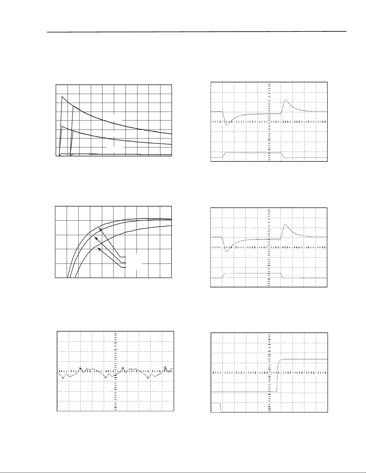
Characteristic Curves
The following figures provide typical characteristics curves for the HW012A0P1 (VO = 1.2 V) module at room temperature (TA
= 25 °C).
0.6
0.5
I
= 12A
O
0.4
0.3
0.2
I
IO = 6A
(V) (200 mV/div)
O
V
OUTPUT VOLT AG
0.1
0
25 30 35 40 45 50 55 60 65 70 7
IO = 0.15A
Figure 1. Input Voltage and Current Characteristics.
84
VI = 36V
V
I
= 48V
82
80
78
76
74
EFFICIENCY, (%)
72
70
02468101
VI = 75V
Figure 2. Converter Efficiency vs. Output Current.
(A) (2 A/div)
O
I
OUTPUT CURRENT,
Figure 4. Transient Response to Step Decrease in
Load from 50% to 25% of Full Load
(VI = 48 Vdc).
(V) (200 mV/div)
O
V
OUTPUT VOLT AG
(A) (5 A/div)
O
I
OUTPUT CURRENT,
Figure 5. Transient Response to Step Increase in
Load from 50% to 75% of Full Load
(VI = 48 Vdc).
(V) (1 V/div)
O
V
OUTPUT VOLT AGE,
(V) (10 mV/div)
O
V
OUTPUT VOLT AG
(V) (5 V/div)
ON/OFF
REMOTE ON/OFF,
V
Figure 3. Output Ripple Voltage (IO = IO, max).
Figure 6. Start-up from Remote On/Off (IO = IO, max).
Lineage Power 6
Page 7
Data Sheet
June 26, 2009
HW006/010/012 Series Power Modules; dc-dc Converters
36-75 Vdc Input; 1.2 Vdc to 5 Vdc Output; 6.6A to 12A
Characteristic Curves
The following figures provide typical characteristics curves for the HW012A0M1 (VO = 1.5 V) module at room temperature (T A =
25 °C)
0.9
0.8
0.7
(A)
I
0.6
0.5
0.4
0.3
0.2
INPUT CURRENT, I
0.1
0
25 30 35 40 45 50 55 60 65 70 75
IO = 12A
IO = 6A
IO = 0.15A
INPUT VOLTAGE, V
I (V)
(V) (100 mV/div)
O
V
OUTPUT VOLT AGE,
(A) (2 A/div)
O
I
OUTPUT CURRENT,
TIME, t (200 ms/div)
Figure 7. Input Voltage and Current Characteristics.
90
88
86
84
82
80
78
76
EFFICIENCY, (%)
74
72
70
024681012
OUTPUT CURRENT, I
O (A)
VI = 36V
V
I = 48V
V
I = 75V
Figure 8. Converter Efficiency vs. Output Current.
Figure 10. Transient Response to Step Decrease in
Load from 50% to 25% of Full Load
(VI = 48 Vdc).
(V) (100 mV/div)
O
V
OUTPUT VOLT AGE,
(A) (5 A/div)
O
I
OUTPUT CURRENT,
TIME, t (200 ms/div)
Figure 11. Transi ent Respon se to S tep Incre ase in Load
from 50% to 75% of Full Load
(VI = 48 Vdc).
(V) (0.5 V/div)
O
V
OUTPUT VOLT AGE,
(V) (10 mV/div)
O
V
OUTPUT VOLT AGE,
(V) (5 V/div)
ON/OFF
REMOTE ON/OFF,
TIME, t (1 µs/div)
Figure 9. Output Ripple Voltage (IO = IO, max).
V
TIME, t (10 ms/div)
Figure 12. Start-up from Remote On/Off (IO = IO, max).
Lineage Power 7
Page 8
Data Sheet
1.2
5
INPUT VOLTAGE, VI (V)
INPUT CURRENT, I
(A)
90
2
OUTPUT CURRENT, IO (A)
TIME, t (1 µs/div)
E,
TIME, t (200 ms/div)
TIME, t (200 ms/div)
TIME, t (10 ms/div)
June 26, 2009
36-75 Vdc Input; 1.2 Vdc to 5 Vdc Output; 6.6A to 12A
HW006/010/012 Series Power Modules; dc-dc Converters
Characteristic Curves
The following figures provide typical characteristics curves for the HW012A0Y1 (VO = 1.8 V) module at room temperature (TA
= 25 °C)
1
I
0.8
0.6
IO = 12A
(V) (100 mV/div)
O
V
OUTPUT VOLT AGE,
0.4
0.2
0
25 30 35 40 45 50 55 60 65 70 7
IO = 6A
IO = 0.15A
Figure 13. Input Voltage and Current Characteristics.
88
86
84
82
80
78
76
EFFICIENCY, (%)
74
72
70
02468101
VI = 36V
V
I
= 48V
V
I
= 75V
Figure 14. Converter Efficiency vs. Output Current.
(A) (2 A/div)
O
I
OUTPUT CURRENT,
Figure 16. Transient Response to Step Decrease in
Load from 50% to 25% of Full Load
(VI = 48 Vdc).
(V) (100 mV/div)
O
V
OUTPUT VOLT AGE,
(A) (5 A/div)
O
I
OUTPUT CURRENT,
Figure 17. Transient Response to Step Increase in
Load from 50% to 75% of Full Load
(VI = 48 Vdc).
(V) (1 V/div)
O
V
OUTPUT VOLT AGE,
(V) (10 mV/div)
O
V
OUTPUT VOLT AG
(V) (5 V/div)
ON/OFF
REMOTE ON/OFF,
V
Figure 15. Output Ripple Voltage (IO = IO, max).
Figure 18. Start-up from Remote On/Off (IO = IO, max).
Lineage Power 8
Page 9
Data Sheet
June 26, 2009
HW006/010/012 Series Power Modules; dc-dc Converters
36-75 Vdc Input; 1.2 Vdc to 5 Vdc Output; 6.6A to 12A
Characteristic Curves
The following figures provide typical characteristics curves for the HW010A0G1 (VO = 2.5 V) module at room temperature (T A =
25 °C)
1.2
1
(A)
I
0.8
0.6
IO = 10A
(V) (100 mV/div)
O
V
OUTPUT VOLT AGE,
0.4
0.2
INPUT CURRENT, I
0
25 30 35 40 45 50 55 60 65 70 75
IO = 5A
IO = 0.05A
I
INPUT VOLTAGE, V
(V)
Figure 19. Input Voltage and Current Characteristics.
95
90
85
80
VI = 36V
V
I
75
EFFICIENCY, (%)
70
012345678910
OUTPUT CURRENT, I
= 48V
V
I
= 75V
O
(A)
Figure 20. Converter Efficiency vs. Output Current.
(A) (5 A/div)
O
I
OUTPUT CURRENT,
TIME, t (100 µs/div)
Figure 22. Transient Response to Step Decrease in
Load from 50% to 25% of Full Load
(VI = 48 Vdc).
(V) (100 mV/div)
O
V
OUTPUT VOLT AGE,
(A) (5 A/div)
O
I
OUTPUT CURRENT,
TIME, t (100 µs/div)
Figure 23. Tra nsient Respon se to S tep In crease in Load
from 50% to 75% of Full Load
(VI = 48 Vdc).
(V) (500 mV/div)
O
V
OUTPUT VOLT AGE,
(V) (10 mV/div)
O
V
OUTPUT VOLT AGE,
(V) (5 V/div)
ON/OFF
REMOTE ON/OFF,
V
TIME, t (1 µs/div)
Figure 21. Output Ripple Voltage (IO = IO, max).
Figure 24. Start-up from Remote On/Off (IO = IO, max).
TIME, t (5 ms/div)
Lineage Power 9
Page 10
Data Sheet
1.6
5
INPUT VOLTAGE, VI (V)
INPUT CURRENT, I
(A)
95
0
OUTPUT CURRENT, IO (A)
TIME, t (1 µs/div)
TIME, t (100 µs/div)
E,
TIME, t (100 µs/div)
E,
TIME, t (5 ms/div)
June 26, 2009
36-75 Vdc Input; 1.2 Vdc to 5 Vdc Output; 6.6A to 12A
HW006/010/012 Series Power Modules; dc-dc Converters
Characteristic Curves
The following figures provide typical characteristics curves for the HW010A0F1 (VO = 3.3 V) module at room temperature (T A
= 25 °C)
1.4
1.2
I
1
0.8
0.6
0.4
0.2
0
25 30 35 40 45 50 55 60 65 70 7
IO = 10A
IO = 5A
IO = 0.05A
(V) (200 mV/div)
O
V
OUTPUT VOLT AG
(A) (5 A/div)
O
I
OUTPUT CURRENT,
Figure 25. Input Voltage and Current Characteristics.
90
85
80
VI = 36V
V
75
EFFICIENCY, (%)
70
01234567891
I = 48V
V
I = 75V
Figure 26. Converter Efficiency vs. Output Current.
Figure 28. Transient Response to Step Decrease in
Load from 50% to 25% of Full Load
(VI = 48 Vdc).
(V) (200 mV/div)
O
V
OUTPUT VOLT AG
(A) (5 A/div)
O
I
OUTPUT CURRENT,
Figure 29. Transient Response to Step Increase in
Load from 50% to 75% of Full Load
(VI = 48 Vdc).
(V) (1 V/div)
O
V
OUTPUT VOLT AGE,
(V) (20 mV/div)
O
V
OUTPUT VOLT AGE,
(V) (5 V/div)
ON/OFF
REMOTE ON/OFF,
V
Figure 27. Output Ripple Voltage (IO = IO, max).
Figure 30. Start-up from Remote On/Off (IO = IO, max).
Lineage Power 10
Page 11

Data Sheet
June 26, 2009
36-75 Vdc Input; 1.2 Vdc to 5 Vdc Output; 6.6A to 12A
HW006/010/012 Series Power Modules; dc-dc Converters
Characteristic Curves
The following figures provide typical characteristics curves for the HW006A6A1 (VO = 5.0 V) module at room temperature (TA =
25 °C)
1.4
1.2
1
0.8
0.6
0.4
INPUT CURRENT, II (A)
0.2
0
25 30 35 40 45 50 55 60 65 70 75
IO = 6.6A
IO = 3.3A
IO = 0.05A
INPUT VOLTAGE, V
I (V)
(V) (200 mV/div)
O
V
OUTPUT VOLT AGE,
(A) (2 A/div)
O
I
OUTPUT CURRENT,
TIME, t (100 µs/div)
Figure 31. Input Voltage and Current Characteristics.
95
90
85
80
VI = 36V
V
I
EFFICIENCY, (%)
75
70
01234567
OUTPUT CURRENT, I
= 48V
V
I
= 75V
O
(A)
Figure 32. Converter Efficiency vs. Output Current.
Figure 34. Transient Response to Step Decrease in
Load from 50% to 25% of Full Load
(VI = 48 Vdc).
(V) (200 mV/div)
O
V
OUTPUT VOLT AGE,
(A) (2 A/div)
O
I
OUTPUT CURRENT,
TIME, t (100 µs/div)
Figure 35. Tra nsient Respon se to S tep In crease in Load
from 50% to 75% of Full Load
(VI = 48 Vdc).
(V) (2 V/div)
O
V
OUTPUT VOLT AGE,
(V) (10m V/div)
O
V
OUTPUT VOLT AGE,
(V) (5 V/div)
ON/OFF
REMOTE ON/OFF,
TIME, t (1 µs/div)
Figure 33. Output Ripple Voltage (IO = IO, max).
V
TIME, t (5 ms/div)
Figure 36. Start-up from Remote On/Off (IO = IO, max).
Lineage Power 11
Page 12
Data Sheet
June 26, 2009
HW006/010/012 Series Power Modules; dc-dc Converters
36-75 Vdc Input; 1.2 Vdc to 5 Vdc Output; 6.6A to 12A
Test Configurations
TO OSCILLOSCOPE
CURRENT
L
TEST
12 µH
S
220 µF
C
BATTERY
ESR < 0.1 Ω
@ 20 ˚C, 100 kHz
Note: Measure input reflected ripple current with a simulated source
inductance (L
TEST) of 12µH. Capacitor CS offsets possible
battery impedance. Measure current as shown above.
Figure 37. Input Reflected Ripple Current Test Setup.
COPPER STRIP
VO(+)
1.0 µF
V
O
(–)
10 µF
GROUND PLANE
Note: Scope measurements should be made using a BNC socket,
with a 10 µF tantalum capacitor and a 1 µF ceramic capcitor.
Position the load between 51 mm and 76 mm (2 in and 3 in)
from the module
Figure 38. Peak-to-Peak Output Ripple Measurement
Test Setup.
VI(+)
I
SUPPLY
CONTACT
RESISTANCE
I
I
(–)
V
Note: All voltage measurements to be taken at the module termi-
nals, as shown above. If sockets are used then Kelvin connections are required at the module terminals to avoid
measurement
errors due to socket contact resistance.
V
V
Figure 39. Output Voltage and Efficiency Test Setup.
–[]I
V
O(+)VO(-)
⎛⎞
η
------------------------------------------------
⎝⎠
V
–[]I
I(+)VI(-)
PROBE
33 µF
ESR < 0.7 Ω
@ 100 kHz
SCOPE
DISTRIBUTION LOSSES
O
(+)
O
(–)
×
O
×
I
RESISTIVE
LOAD
CONTACT AND
I
O
100×=
I
(+)
V
V
I
(-)
LOAD
Safety Considerations
For safety-agency approval of the system in which the power
module is used, the power module must be installed in compliance with the spacing and separation requirements of the
end-use safety agency standard, i.e., UL60950, CSA C22.2
No. 60950-00, and
VDE 0805:2001-12 (IEC60950, 3rd Ed).
These converters have been evaluated to the spacing
requirements for Basic Insulation, per the above safety standards.
For Basic Insulation models ("–B" Suffix), 1500 Vdc is
applied from VI to VO to 100% of outgoing production.
For end products connected to –48 Vdc, or –60 Vdc nomianl
DC MAINS (i.e. central office dc battery plant), no further
fault testing is required.
Note:–60 V dc nominal bettery plants are not available in the
U.S. or Canada.
For all input voltages, other than DC MAINS, where the input
voltage is less than 60 Vdc, if the input meets all of the
requirements for SELV, then:
n
The output may be considered SELV. Output voltages will
remain withing SELV limits even with internally-generated
non-SELV voltages. Single component failure and fault
tests were performed in the power converters.
n
One pole of the input and one pole of the output are to be
grounded, or both circuits are to be kept floating, to maintain the output voltage to ground voltage within ELV or
SELV limits.
For all input sources, other than DC MAINS, where the input
voltage is between 60 and 75 Vdc (Classified as TNV-2 in
Europe), the following must be adhered to, if the converter’s
output is to be evaluated for SELV:
n
The input source is to be provided with reinforced insulation from any hazardous voltage, including the AC mains.
n
One VI pin and one VO pin are to be reliably earthed, or
both the input and output pins are to be kept floating.
n
Another SELV reliability test is conducted on the whole
system, as required by the safety agencies, on the combination of supply source and the subject module to verify
that under a single fault, hazardous voltages do not
appear at the module’s output.
The power module has ELV (extra-low voltage) outputs
when all inputs are ELV.
All flammable materials used in the manufacturing of these
modules are rated 94V-0, and UL60950A.2 for reduced
thicknesses. The input to these units is to be provided with a
maximum 5A time-delay in the unearthed lead.
Lineage Power 12
Page 13
Data Sheet
June 26, 2009
HW006/010/012 Series Power Modules; dc-dc Converters
36-75 Vdc Input; 1.2 Vdc to 5 Vdc Output; 6.6A to 12A
Design Considerations
Input Source Impedance
The power module should be connected to a low
ac-impedance source. A highly inductive source impedance
can affect the stability of the power module. For the test configuration in Figure 37, a 33µF electrolytic capacitor
(ESR<0.7W at 100kHz), mounted close to the power module
helps ensure the stability of the unit. Consult the factory for
further application guidelines.
Feature Descriptions
Remote On/Off
Two remote On/Off options are available. Positive logic
remote On/Off turns the module on during a logic-high voltage on the remote ON/OFF pin, and off during a logic low.
Negative logic remote On/Off, device code suffix "1", turns
the module off during logic-high voltage and on during a logic
low.
To turn the power module on and off, the user must supply a
switch to control the voltage betw e en the
ON/OFF pin and the VI(–) terminal. The switch may be an
open collector or equivalent (see Figure 40). A logic low is
Von/off = –0.7 V to 1.2 V. The maximum Ion/off during a logic
low is 1 mA. The switch should maintain a logic-low voltage
while sinking 1 mA. During a logic high, the maximum Von/off
generated by the power module is 15 V. The maximum allowable leakage current of the switch at Von/off = 15 V is 50 µA.
If not using the remote on/off feature, do one of the following:
For positive logic, leave the ON/OFF pin open.
For negative logic, short the ON/OFF pin to VI(–).
Ion/off
ON/OFF
+
Von/off
–
VO(+)
O(–)
V
I(+)
I(–)
V
V
LOAD
Output Voltage Set-Point Adjustment (Trim)
Output voltage trim allows the user to increase or decrease
the output voltage set point of a module. This is accomplished by connecting an external resistor between the TRIM
pin and either the VO(+) or VO(–) pins. The trim resistor
should be positioned close to the module. If not using the trim
feature, leave the TRIM pin open.
With an external resistor Trim-down between the TRIM and
VO(–) pins, the output voltage set point VO, set decreases
(see Figure 41). The following equation determines the
required external-resistor value to trim-down the output voltage from VO, set to VO:
⎧⎫
A
R
trim-down
Rtrim-down is the external resistor in kW
D% is the % change in output voltage
A & B are defined in Table 1 for various models
Table 1
⎨⎬
⎩⎭
Output Voltage
(V)
-------- -
Δ%
B–
kΩ=
AB
1.2 1089 62.0
1.5 1089 104
1.8 1089 104
2.5 1690 73.1
3.3 1690 73.1
5.0 1690 73.1
For example, to trim-down the output voltge of 2.5 V module
(HW010A0G) by 8% to 2.3 V , Rtrim-down is calculated as follows:
D% = 8
A = 1690
B = 73.1
⎧⎫
R
trim-down
R
trim down–
1690
----------- -
⎨⎬
⎩⎭
73.1–
8
kΩ=
138.15kΩ=
Figure 40. Remote On/Off Implementation.
Lineage Power 13
Page 14

Data Sheet
D
June 26, 2009
Feature Descriptions (continued)
HW006/010/012 Series Power Modules; dc-dc Converters
36-75 Vdc Input; 1.2 Vdc to 5 Vdc Output; 6.6A to 12A
Output Voltage Set-Point Adjustment
(Trim) (continued)
VI(+)
ON/OFF
V
I(–)
Figure 41. Circuit Configuration to Decrease Output
With an external resistor Rtrim-up, connected between the
TRIM and VO(+) pins, the output voltage set point VO, set
increases (see Fiugre 42). The following equation determines the required external-resistor value to trim-up the output voltage from VO, set to VO:
R
trim-up
Rtrim-up is the external resistor in kW
D% is the % change in output voltage
A, B and C are defined in Table 2
Tab le 2
Output Voltage
(V)
1.2 15.9 1089 62.0
1.5 19.8 1089 104
1.8 23.8 1089 104
2.5 34.5 1690 73.1
3.3 45.5 1690 73.1
5.0 69.0 1690 73.1
For example, to trim-up the output voltage of 1.5 V module
(HW012A0M) by 8% to 1.62 V, Rtrim-up is calcualted is as
follows:
D% = 8
A = 19.8
B = 1089
C = 104
O(+)
V
TRIM
Rtrim-down
O(–)
V
Voltage.
⎧⎫
A 100 Δ%+()B–
------------------------------------------ -
⎨⎬
⎩⎭
Δ%
C–
ABC
RLOAD
kΩ=
VI(+)
ON/OFF
V
I(–)
Figure 42. Circuit Configuration to Increase
The amount of power delivered by the module is defined as
the voltage at the output terminals multiplied by the output
current. When using trim, the output voltage of the module
can be increased, which at the same output current would
increase the power output of the module. Care should be
taken to ensure that the maximum output power of the module remains at or below the maximum rated power (maximum rated power = VO, set x IO, max).
O(+)
V
TRIM
O(–)
V
Output Voltage.
Rtrim-up
RLOA
Overcurrent Protection
To provide protection in an output overload fault condition,
the module is equipped with internal current-limiting circuitry,
and can endure current limiting for an unlimited duration. At
the instance of current-limit inception, the module enters a
"hiccup" mode of operation, whereby it shuts down and automatically attempts to restart. While the fault condition exists,
the module will remain in this mode until the fault is cleared.
The unit operates normally once the output current is
reduced back into its specified range.
Output Overvoltage Protection
The output overvoltage protection clamp consists of control
circuitry, independent of the primary regulation loop, that
monitors the voltage on the output terminals. This control
loop has a higher voltage set point than the primary loop
(See the overvoltage clamp values in the Feature Specifications Table). In a fault condition, the overvoltage clamp
ensures that the output voltage does not exceed VO, ovsd,
max. This provides a redundant voltage-control that reduces
the risk of output overvoltage.
⎧⎫
R
trim-up
R
trim-up
Lineage Power 14
19.8 100 8+()1089–
--------------------------------------------------- -
⎨⎬
⎩⎭
27.175kΩ=
8
104–
kΩ=
Page 15

Data Sheet
June 26, 2009
HW006/010/012 Series Power Modules; dc-dc Converters
36-75 Vdc Input; 1.2 Vdc to 5 Vdc Output; 6.6A to 12A
Feature Descriptions (continued)
Overtemperature Protection
To provide protection under certain fault conditios, the unit is
equipped with a thermal shutdown circuit. The unit will shudown if the overtemperature threshold is exceeded, but the
thermal shut down is not intended as a guarantee that the
unit will survive temperatures beyond its rating. The module
will automatically restart after it cools down.
Input Undervoltage Lockout
At input voltages below the input undervoltage lockout limit,
the module operation is disabled. The module will begin to
operate at an input voltage above the undervoltage lockout
turn-on threshold.
Lineage Power 15
Page 16

Data Sheet
to drain lead.
0
Ambient Temperature T
(˚C)
8
0
OUTPUT CURRENT, I
(A)
0
OUTPUT CURRENT, I
(A)
June 26, 2009
HW006/010/012 Series Power Modules; dc-dc Converters
36-75 Vdc Input; 1.2 Vdc to 5 Vdc Output; 6.6A to 12A
Thermal Considerations
The power modules operate in a variety of thermal environments; however, sufficient cooling should be provided to help
ensure reliable operation of the unit. Heat is removed by conduction, convection, and radiation to the surrounding environment. Proper cooling can be verified by measuring drain pin
Q203 at the position indicated in Figure 43.
The temperature at Q203 drain pins should not exceed 115
°C. The output power of the module should not exceed the
rated power for the module
(VO, set x IO, max).
Although the maximum operating ambient temperature of the
power modules is 85 °C, you can limit this temperature to a
lower value for extremely high reliability.
12
10
(A)
8
O
6
4
Output Current I
2
0
20 30 40 50 60 70 80 9
2.0 m/s (400 ft./min.)
1.0 m/s (200 ft./min.)
0.5 m/s (100 ft./min.)
NATURAL CONVECTION
A
Figure 44. Derating Curves for HW010A0F1
(VO = 3.3 V) in Transverse Orientation
(VI = 48 Vdc).
7
6
Q203
Attach thermocouple
AIRFLOW
Figure 43. HW 6.6A-12A-Series Temperature
Measurement Location (Top View).
Heat T ransfer via Convection
Increasing airflow over the module enhances the heat transfer via convection. Figures 44—48 show the maximum cur-
O
5
4
3
2
1
0
20 30 40 50 60 70 80 9
2.0 m/s (400 ft./min.)
1.0 m/s (200 ft./min.)
0.5 m/s (100 ft./min.)
NATURAL CONVECTION
AMBIENT TEMPERA TURE, TA (˚C)
Figure 45. Derating Curves for HW006A6A1
(VO = 5.0 V) in Transverse Orientation
(VI = 48 Vdc).
rent that can be delivered by various modules versus local
ambient temperature (TA) for natural convection through 2 m/
s (400 ft./min.).
Systems in which these power modules may be used typically generate natural convection airflow rates of 0.3 ms
–1
(60 ft./min.) due to other heat-dissipating components in the
system. Therefore, the natural convection condition represents airflow rates of up to 0.3 ms
–1
(60 ft./min.). Use of Fig-
ure 44 is shown in the following example.
Example
What is the minimum airflow necessary for a HW010A0F1
operating at VIN = 48 V, an output current of 10 A, and a
maximum ambient temperature of 75 °C.
Solution
Given: VIN = 48V
IO = 12 A
TA = 75 °C
11
10
9
O
8
7
6
5
4
3
2
1
0
20 30 40 50 60 70 80 9
2.0 m/s (400 ft./min.)
1.0 m/s (200 ft./min.)
0.5 m/s (100 ft./min.)
NATURAL CONVECTION
AMBIENT TEMPERA TURE, TA (˚C)
Figure 46. Derating Curves for HW010A0G1
(VO = 2.5 V) in Transverse Orientation
(VI = 48 Vdc).
Determine airflow (v) (Use Figure 44.):
v = 0.5 m/s (100 ft./min.)
Lineage Power 16
Page 17

Data Sheet
HW006/010/012 Series Power Modules; dc-dc Converters
June 26, 2009
Thermal Considerations (continued)
Figure 47. Derating Curves for HW012A0Y1
(VO = 1.8 V) in Transverse Orientation
(VI = 48 Vdc).
36-75 Vdc Input; 1.2 Vdc to 5 Vdc Output; 6.6A to 12A
Figure 48. Derating Curves for HW012A0P1
(VO = 1.2 V) in Transverse Orientation
(VI = 48 Vdc).
Layout Considerations
Copper paths must not be routed beneath the power module.
For additional layout guidelines, refer to the FLTR100V10 or
FLTR100V20 data sheet.
EMC Considerations
For assistance with designing for EMC compliance, please
refer to the FLTR100V10 data sheet
(FDS01-043EPS)
Lineage Power 17
Page 18

Data Sheet
June 26, 2009
HW006/010/012 Series Power Modules; dc-dc Converters
36-75 Vdc Input; 1.2 Vdc to 5 Vdc Output; 6.6A to 12A
Through-Hole Lead-Free Soldering Information
The RoHS-compliant through-hole products use the SAC
(Sn/Ag/Cu) Pb-free solder and RoHS-compliant components.
They are designed to be processed through single or dual
wave soldering machines. The pins have an RoHS-compliant finish that is compatible with both Pb and Pb-free wave
soldering processes. A maximum preheat rate of 3°C/s is
suggested. The wave preheat process should be such that
the temperature of the power module board is kept below
210°C. For Pb solder, the recommended pot temperature is
260°C, while the Pb-free solder pot is 270°C max. Not all
RoHS-compliant through-hole products can be processed
with paste-through-hole Pb or Pb-free reflow process. If
additional information is needed, please consult with your
Lineage Power representative for more details.
Surface Mount Information
Pick and Place Area
Although the module weight is minimized by using openframe construction, the modules have a relatively large mass
compared to conventional surface-mount components. T o
optimize the pick-and-place process, automated vacuum
equipment variables such as
nozzle size, tip style, vacuum pressure, and placement
speed should be considered. Surface-mount versions of this
family have a flat surface which serves as a
pick-and-place location for automated vacuum equipment.
The module’s pick-and-place location is identified in Figure
49.
sure and placement speed should be considered to optimize
this process.
The minimum recommended nozzle diameter for reliable
operation is 6mm. The maximum nozzle outer diameter,
which will safely fit within the allowable component spacing,
is 9 mm.
Oblong or oval nozzles up to 11 x 9 mm may also be used
within the space available.
For further information please contact your local Lineage
Power Technical Sales Representative.
Reflow Soldering Information
The HW006 family of power modules is available for either
Through-Hole (TH) or Surface Mount (SMT) soldering.
These power modules are large mass, low thermal resistance devices and typically heat up slower than other SMT
components. It is recommended that the customer review
data sheets in orde r to customize the solder reflow profile for
each application board assembly.
The following instructions must be observed when SMT soldering these units. Failure to observe these instructions may
result in the failure of or cause damage to the modules, and
can adversely affect long-term reliability.
The surface mountable modules in the HW006 family use our
newest SMT technology called "Col umn Pin" (CP) connectors. Figure 50 shows the new CP connector before and after
reflow soldering onto the end-board assembly.
HW006 Board
Insulator
Solder Ball
End assembly PCB
X
14mm
(0.57in)
21mm
(0.84in)
Figure 49. Pick and Place Location.
Z Plane Height
The 'Z' plane height of the pick and place location is 7.50mm
nominal with an RSS tolerance of +/-0.25 mm.
Nozzle Recommendations
The module weight has been kept to a minimum by using
open frame construction. Even so, they have a relatively
large mass when compared with conventional SMT components. Variables such as nozzle size, tip style, vacuum pres-
Lineage Power 18
Figure 50. Column Pin Connector Before and After
Reflow Soldering.
The CP is constructed from a solid copper pin with an integral
solder ball attached, which is composed of tin/lead (Sn/Pb)
solder. The CP connector design is able to compensate for
large amounts of co-planarity and still ensure a reliable SMT
solder joint.
Typically, the eutectic solder melts at 183oC, wets the land,
and subsequently wicks the device connection. Sufficient
time must be allowed to fuse the plating on the connection to
ensure a reliable solder joint. There are several types of
SMT reflow technologies currently used in the industry.
These surface mount power modules can be reliably soldered using natural forced convection, IR (radiant infrared),
or a combination of convection/IR. For reliable soldering the
solder reflow profile should be established by accurately
measuring the modules CP connector temperatures.
Page 19
Data Sheet
June 26, 2009
300
250
200
150
100
50
0
Peak Temp 235
Heat zone
o
max 4
Cs
Preheat zone
o
max 4
REFLOW TIME (S)
-1
Soak zone
30-240s
-1
Cs
o
C
HW006/010/012 Series Power Modules; dc-dc Converters
36-75 Vdc Input; 1.2 Vdc to 5 Vdc Output; 6.6A to 12A
Cooling
zone
oCs-1
1-4
T
above
lim
o
C
205
Figure 51. Recommended Reflow profile.
240
235
230
225
220
215
210
205
200
0
10
20
30
40
0
C.
50 60
TIME (S)
Figure 52. Time Limit curve above 205
Lead Free Soldering
The -Z version SMT modules of the HW/HC series are leadfree (Pb-free) and RoHS compliant and are compatible in a
Pb-free soldering process. Failure to observe the instructions
below may result in the failure of or cause damage to the
modules and can adversely affect long-term reliability.
ages should not be broken until time of use. Once the original package is broken, the floor life of the product at
conditions of < 30°C and 60% relative humidity varies according to the MSL rating (see J-STD-033A). The shelf life for dry
packed SMT packages will be a minimum of 12 months from
the bag seal date, when stored at the following conditions: <
40° C, < 90% relative humidity.
Post Solder Cleaning and Drying Considerations
Post solder cleaning is usually the final circuit-board
assembly process prior to electrical board testing. The result
of inadequate cleaning and drying can affect both the
reliability of a power module and the testability of the finished
circuit-board assembly. For guidance on appropriate
soldering, cleaning and drying procedures, refer to Lineage
Power Board Mounted Power Modules: Soldering and
Cleaning Application Note (AP01-056EPS).
Per J-STD-02 0 Rev. C
300
250
200
150
Heating
Zone
100
Reflow Temp (°C)
50
0
Peak Temp
Cooling
Zone
* Min. Time
Ab ov e 235°C
*Time Above
217°C
Reflow Time (Seconds)
Figure 53. Recommended linear reflow profile usin g Sn/
Ag/Cu solder.
Solder Ball and Cleanliness Requirements
The open frame (no case or potting) power module will meet
the solder ball requirements per J-STD-001B. These requirements state that solder balls must neither be loose nor violate
the power module minimum electrical spacing.
The cleanliness designator of the open frame power module
is C00 (per J specification).
Pb-free Reflow Profile
Power Systems will comply with J-STD-020 Rev. C (Moisture/
Reflow Sensitivity Classification for Nonhermetic Solid State
Surface Mount Devices) for both Pb-free solder profiles and
MSL classification procedures. This standard provides a recommended forced-air-convection reflow profile based on the
volume and thickness of the package (table 4-2). The suggested Pb-free solder paste is Sn/Ag/Cu (SAC). The recommended linear reflow profile using Sn/Ag/Cu solder is shown
in Figure. 53.
MSL Rating
The HW series SMT modules have a MSL rating of 1.
Storage and Handling
The recommended storage environment and handling procedures for moisture-sensitive surface mount packages is
detailed in J-STD-033 Rev. A (Handling, Packing, Shipping
and Use of Moisture/Reflow Sensitive Surface Mount
Devices). Moisture barrier bags (MBB) with desiccant are
required for MSL ratings of 2 or greater. These sealed pack-
Lineage Power 19
Page 20

Data Sheet
T
S
B
6
r
June 26, 2009
HW006/010/012 Series Power Modules; dc-dc Converters
36-75 Vdc Input; 1.2 Vdc to 5 Vdc Output; 6.6A to 12A
Outline Diagram for Surface-Mount Module
Dimensions are in millimeters and (inches).
Tolerances: x.x mm ± 0.5 mm (x.xx in. ± 0.02 in.) [unless otherwise indicated]
x.xx mm ± 0.25 mm (x.xxx in. ± 0.010 in.)
47.2
op View
29.5
(1.16)
(1.86)
0.06 x 0.0
chamffe
ide View
ottom View
2.54
(0.100)
min stand-off
height
0.5
(.020)
max
compliance
1.7
(0.07)
26.16
(1.030)
5.00
(0.197)
V
O+VO-
V
I+VI-
8.50
(0.335)
MAX
3.6
(0.14)
TRIM
On/Off
35.00
(1.375)
40.00
(1.575)
Lineage Power 20
Page 21

Data Sheet
June 26, 2009
HW006/010/012 Series Power Modules; dc-dc Converters
36-75 Vdc Input; 1.2 Vdc to 5 Vdc Output; 6.6A to 12A
Outline Diagram for Through-Hole Module
Dimensions are in millimeters and (inches).
Tolerances: x.x mm ± 0.5 mm (x.xx in. ± 0.02 in.) [unless otherwise indicated]
x.xx mm ± 0.25 mm (x.xxx in. ± 0.010 in.)
Lineage Power 21
Page 22
Data Sheet
2
2
)
)
1)
0)
0.110" SOLDER MASK OPENING
a.
June 26, 2009
HW006/010/012 Series Power Modules; dc-dc Converters
36-75 Vdc Input; 1.2 Vdc to 5 Vdc Output; 6.6A to 12A
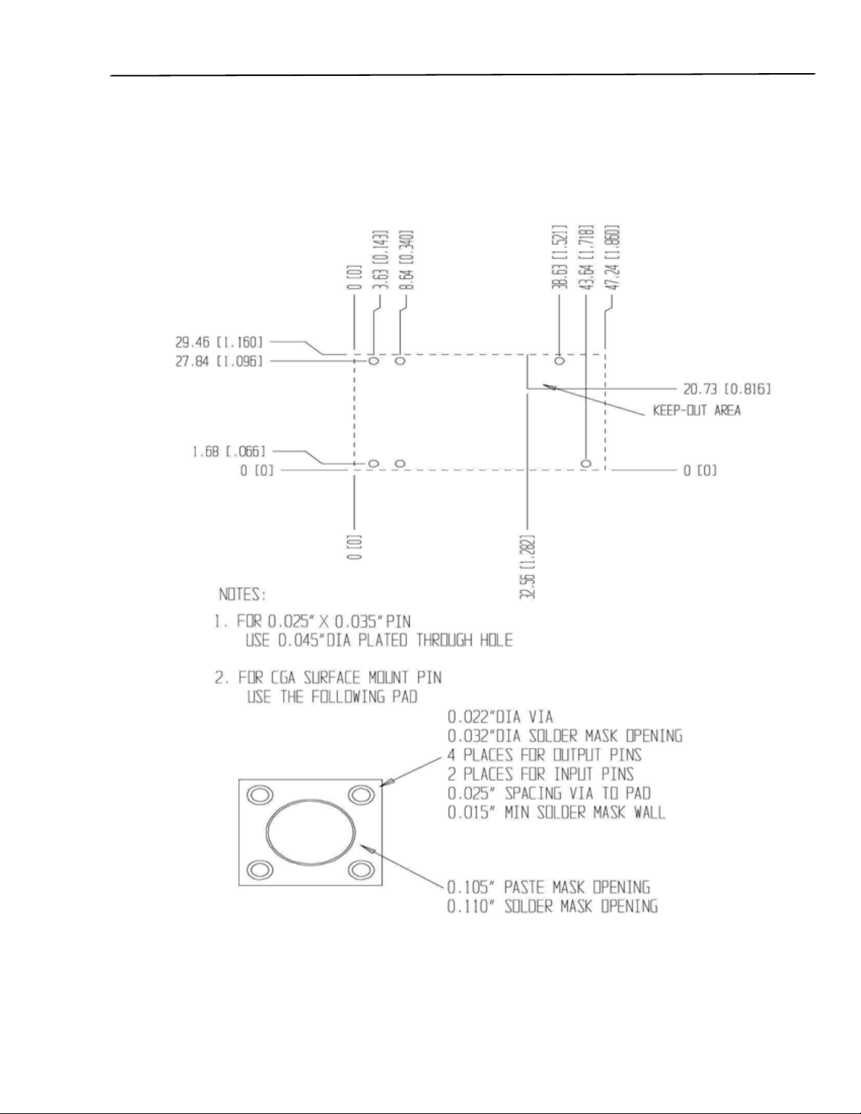
Recommended Pad Layout for Surface-Mount Module
and Recommended Hole Layout for Through-Hole Module
Component-side footprint.
Dimensions are in millimeters and (inches), unless otherwise noted.
0 (0)
3.63 (0.143
9.46 (1.160)
7.84 (1.096)
1.68 (0.066)
0 (0)
8.64 (0.340
38.63 (1.52
43.64 (1.718)47.24 (1.86
20.73 (0.816)
KEEP-OUT AREA:
Besides trace to ON/OFF pin,
do not route other traces on the
PWB top layer closest to the
power module in this keep-out are
0 (0)
0 (0)
NOTES:
1. FOR CGA SURFACE MOUNT PIN
USE THE FOLLOWING PAD
32.56 (1.282)
0.022" DIA VIA
0.032" DIA SOLDER MASK OPENING
4 PLACES FOR OUTPUT PINS
2 PLACES FOR INPUT PINS
0.025" SPACING VIA TO PAD
0.015" MIN SOLDER MASK WALL
0.105" PASTE MASK OPENING
Lineage Power 22
Page 23

Data Sheet
June 26, 2009
HW006/010/012 Series Power Modules; dc-dc Converters
36-75 Vdc Input; 1.2 Vdc to 5 Vdc Output; 6.6A to 12A
Ordering Information
Please contact your Lineage Power Sales Representative for pricing, availability and optional features.
Table 1. Device Codes
Input Volt age
Output
Voltage
Output
Current
Efficiency Connector Type Device Code Comcodes
36 – 75 Vdc 1.2 V 12 A 82 Through-Hole HW012A0P1 108965591
36 – 75 Vdc 1.5 V 12 A 83 Through-Hole HW012A0M1 108968389
36 – 75 Vdc 1.8 V 12 A 85 Through-Hole HW012A0Y1 108968405
36 – 75 Vdc 2.5 V 10 A 89 Through-Hole HW010A0G1 108968421
36 – 75 Vdc 3.3 V 10 A 90 Through-Hole HW010A0F1 108965625
36 – 75 Vdc 3.3 V 10 A 90 Through-Hole HW010A0F1Z CC109107141
36 – 75 Vdc 5.0 V 6 A 91 Through-Hole HW006A6A1 108968363
36 – 75 Vdc 5.0 V 6 A 91 Through-Hole HW006A6A1Z CC109107133
36 – 75 Vdc 1.2 V 12 A 82 SMT HW012A0P1-S 108965617
36 – 75 Vdc 1.2 V 12 A 82 SMT HW012A0P1-SZ 109100360
36 – 75 Vdc 1.5 V 12 A 83 SMT HW012A0M1-S 108968371
36 – 75 Vdc 1.5 V 12 A 83 SMT HW012A0M1-SZ CC109101805
36 – 75 Vdc 1.8 V 12 A 85 SMT HW012A0Y1-S 108968397
36 – 75 Vdc 1.8 V 12 A 85 SMT HW012A0Y1-SZ 109100377
36 – 75 Vdc 2.5 V 10 A 89 SMT HW010A0G1-S 108968413
36 – 75 Vdc 3.3 V 10 A 90 SMT HW010A0F1-S 108967985
36 – 75 Vdc 3.3 V 10 A 90 SMT HW010A0F1-SZ 108995214
36 – 75 Vdc 5.0 V 6 A 91 SMT HW006A6A1-S 108968355
36 – 75 Vdc 5.0 V 6 A 91 SMT HW006A6A-S CC109142155
36 – 75 Vdc 5.0 V 6 A 91 SMT HW006A6A1-SZ 109100352
Optional features can be ordered using the suffixes shown below. The suffixes follow the last letter of the Product Code and are
placed in descending alphanumerical order.
Table 2. Device Options
Option Suffix
Negative remote on/off logic 1
Approved for Basic Insulation –B
Surface mount interconnections –S
RoHS Compliant -Z
Asia-Pacific Headquart er s
Tel: +65 6 416 4283
W orld Wide Headquarter s
Lin ea g e Power Co rpor at io n
3000 Skyli ne Drive, Mesquite, TX 75149, USA
+1-800-526-7819
(Outside U.S.A.: +1-972-284-2626)
www.lineagepower.com
e-mail: techsupport1@lineagepower.com
Lineage Power reserves the right to make changes to the product(s) or information contained herein without notice. No liability is assumed as a result of their use or
application. No rights under any patent acc ompany the sale of any such product(s) or information.
© 2008 Lineage Power Corporation, (Mesquite, Texas) All International Rights Reserved.
Europe, M iddle-East and Afric a Headquarters
Tel: +49 8 9 6089 286
India Head quarters
Tel: +91 8 0 28411633
Document No: ADS02-006EPS ver.1.4
PDF Name: fds03-0031.pdf
 Loading...