

Page 1
Data Sheet
October 2, 2009
8.3 – 14Vdc Input; 0.75Vdc to 5.5 Vdc Output; 3A Output Current
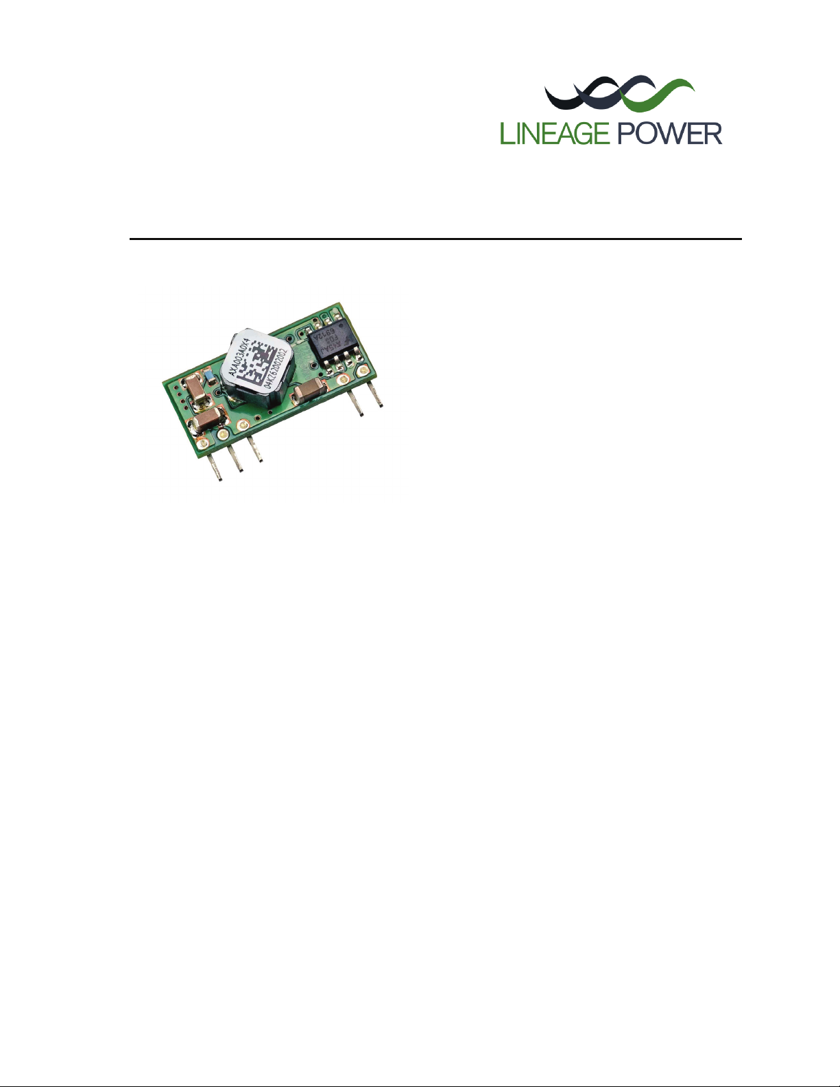
Austin MinilynxTM 12V SIP Non-isolated Power Modules:
RoHS Compliant
Applications
Distributed power architectures
Intermediate bus voltage applications
Telecommunications equipment
Servers and storage applications
Networking equipment
Enterprise Networks
Latest generation IC’s (DSP, FPGA, ASIC) and
Microprocessor powered applications
Features
Compliant to RoHS EU Directive 2002/95/EC (-Z
versions)
Compliant to ROHS EU Directive 2002/95/EC with
lead solder exemption (non-Z versions)
Delivers up to 3A output current
High efficiency – 91% at 3.3V full load (V
Small size and low profile:
22.9 mm x 10.2 mm x 6.63 mm
(0.90 in x 0.4in x 0.261 in)
Low output ripple and noise
High Reliability:
Calculated MTBF = 10.8M hours at 25
Constant switching frequency (300 kHz)
Output voltage programmable from 0.75 Vdc to 5.5
Vdc via external resistor
Line Regulation: 0.3% (typical)
Load Regulation: 0.4% (typical)
Temperature Regulation: 0.4 % (typical)
Remote On/Off
Output overcurrent protection (non-latching)
Wide operating temperature range (-40°C to 85°C)
†
UL* 60950-1Recognized, CSA
60950-1-03 Certified, and VDE
(EN60950-1) Licensed
ISO** 9001 and ISO 14001 certified manufacturing
facilities
C22.2 No.
‡
0805:2001-12
= 12.0V)
IN
o
C Full-load
Description
Austin MiniLynxTM 12V SIP (single-inline) power modules are non-isolated DC-DC converters that can deliver up to
3A of output current with full load efficiency of 91% at 3.3V output. These modules provide precisely regulated
output voltage programmable via external resistor from 0.75Vdc to 5.5Vdc over a wide range of input voltage (V
8.3 - 14V). Their open-frame construction and small footprint enable designers to develop cost- and space-efficient
solutions. In addition to sequencing, standard features include remote On/Off, programmable output voltage and
over current protection.
* UL is a re gistered trademark of Underwriters Laboratories, Inc.
†
CSA is a reg istered trademark of Canadian Standards Associ ation.
‡
VDE is a t rademark of Verband Deutscher Elektrotechniker e.V.
** ISO is a registered trademark of the International Or ganization of Standards
Document No: DS04-041 ver. 1.32
PDF name: minilynx_sip_12v_ds.pdf
=
IN
Page 2

Data Sheet
October 2, 2009
Austin MiniLynx
8.3 – 14Vdc Input; 0.75Vdc to 5.5Vdc Output; 3A output current
TM
12V SIP Non-isolated Power Modules:
Absolute Maximum Ratings
Stresses in excess of the absolute maximum ratings can cause permanent damage to the device. These are
absolute stress ratings only, functional operation of the device is not implied at these or any other conditions in
excess of those given in the operations sections of the data sheet. Exposure to absolute maximum ratings for
extended periods can adversely affect the device reliability.
Parameter Device Symbol Min Max Unit
Input Voltage All V
Continuous
Operating Ambient Temperature All T
IN
A
-0.3 15 Vdc
-40 85 °C
(see Thermal Considerations section)
Storage Temperature All T
stg
-55 125 °C
Electrical Specifications
Unless otherwise indicated, specifications apply over all operating input voltage, resistive load, and temperature
conditions.
Parameter Device Symbol Min Typ Max Unit
Operating Input Voltage Vo,set ≤ 3.63 VIN 8.3 12 14 Vdc
Vo,set > 3.63 VIN 8.3 12 13.2 Vdc
Maximum Input Current All I
(VIN= V
Input No Load Current V
(VIN = V
IN, min
to V
IN, nom
IN, max
, IO=I
O, max VO,set
= 3.3Vdc)
Vdc, IO = 0, module enabled) V
= 0.75Vdc I
O,set
= 5.5Vdc I
O,set
IN,max
IN,No load
IN,No load
2.2 Adc
45 mA
150 mA
Input Stand-by Current All I
(VIN = V
, module disabled)
IN, nom
1.2 mA
IN,stand-by
Inrush Transient All I2t 0.4 A2s
Input Reflected Ripple Current, peak-to-peak
(5Hz to 20MHz, 1μH source impedance; V
V
= I
IN, max, IO
; See Test configuration section)
Omax
IN, min
to
All 30 mAp-p
Input Ripple Rejection (120Hz) All 30 dB
CAUTION: This power module is not internally fused. An input line fuse must always be used.
This power module can be used in a wide variety of applications, ranging from simple standalone operation to being
part of a complex power architecture. To preserve maximum flexibility, internal fusing is not included, however, to
achieve maximum safety and system protection, always use an input line fuse. The safety agencies require a fastacting fuse with a maximum rating of 6 A (see Safety Considerations section). Based on the information provided in
this data sheet on inrush energy and maximum dc input current, the same type of fuse with a lower rating can be
used. Refer to the fuse manufacturer’s data sheet for further information.
LINEAGE POWER 2
Page 3

Data Sheet
October 2, 2009
Austin MiniLynx
8.3 – 14Vdc Input; 0.75Vdc to 5.5Vdc Output; 3A output current
TM
12V SIP Non-isolated Power Modules:
Electrical Specifications (continued)
Parameter Device Symbol Min Typ Max Unit
Output Voltage Set-point All V
(VIN=V
IN, min
, IO=I
, TA=25°C)
O, max
Output Voltage All V
(Over all operating input voltage, resistive load,
and temperature conditions until end of life)
Adjustment Range All V
Selected by an external resistor
O, set
O, set
O
Output Regulation
Line (VIN=V
Load (IO=I
Temperature (T
IN, min
O, min
to V
to I
ref=TA, min
) All
IN, max
) All
O, max
to T
) All ⎯ 0.4
A, max
Output Ripple and Noise on nominal output
(VIN=V
IN, nom
and IO=I
O, min
to I
O, max
Cout = 1μF ceramic//10μFtantalum capacitors)
RMS (5Hz to 20MHz bandwidth) All
Peak-to-Peak (5Hz to 20MHz bandwidth) All
External Capacitance
ESR ≥ 1 mΩ All C
ESR ≥ 10 mΩ All C
Output Current All I
Output Current Limit Inception (Hiccup Mode ) All I
(VO= 90% of V
)
O, set
Output Short-Circuit Current All I
(VO≤250mV) ( Hiccup Mode )
Efficiency V
VIN= V
IO=I
, TA=25°C V
IN, nom
= V
O, max , VO
V
O,set
V
V
V
= 1.2Vdc η 81.5 %
O,set
= 1.5Vdc η 84.0 %
O, set
= 1.8Vdc η 86.0 %
O,set
= 2.5Vdc η 89.0 %
O,set
= 3.3Vdc η 91.0 %
O,set
= 5.0Vdc η 93.0 %
O,set
Switching Frequency All f
O, max
O, max
o
O, lim
O, s/c
sw
Dynamic Load Response
(dIo/dt=2.5A/μs; VIN = V
IN, nom
; TA=25°C)
Load Change from Io= 50% to 100% of
Io,max; 1μF ceramic// 10 μF tantalum
All V
pk
Peak Deviation
Settling Time (Vo<10% peak deviation)
(dIo/dt=2.5A/μs; VIN = V
IN, nom
; TA=25°C)
Load Change from Io= 100% to 50%of Io,max:
1μF ceramic// 10 μF tantalum
All t
All V
s
pk
Peak Deviation
Settling Time (Vo<10% peak deviation)
All t
s
-2.5 V
-3%
+2.5 % V
O, set
⎯
+4% % V
0.7525 5.5 Vdc
⎯
⎯
⎯
⎯
0.3
0.4
⎯
⎯
⎯
10 15 mV
30 50 mV
% V
% V
% V
⎯ ⎯
⎯ ⎯
1000 μF
3000 μF
0 3 Adc
⎯
⎯
200
2
⎯
⎯
⎯
⎯
⎯
⎯
⎯
300
200
25
200
25
⎯
⎯
⎯ μs
⎯
⎯ μs
O, set
O, set
O, set
O, set
O, set
pk-pk
% I
Adc
kHz
mV
mV
rms
o
LINEAGE POWER 3
Page 4
Data Sheet
October 2, 2009
Austin MiniLynx
8.3 – 14Vdc Input; 0.75Vdc to 5.5Vdc Output; 3A output current
TM
12V SIP Non-isolated Power Modules:
Electrical Specifications (continued)
Parameter Device Symbol Min Typ Max Unit
Dynamic Load Response
(dIo/dt=2.5A/μs; V VIN = V
Load Change from Io= 50% to 100% of Io,max;
Co = 2x150 μF polymer capacitors
Peak Deviation
Settling Time (Vo<10% peak deviation)
(dIo/dt=2.5A/μs; VIN = V
Load Change from Io= 100% to 50%of Io,max:
Co = 2x150 μF polymer capacitors
Peak Deviation
Settling Time (Vo<10% peak deviation)
IN, nom
IN, nom
; TA=25°C)
; TA=25°C)
All V
All t
All V
All t
pk
s
pk
s
⎯
⎯
⎯
⎯
75
100
75
100
⎯
⎯ μs
⎯
⎯ μs
mV
mV
General Specifications
Parameter Min Typ Max Unit
Calculated MTBF (IO=I
per Telecordia SR-332 Issue 1: Method 1 Case 3
Weight
, TA=25°C)
O, max
⎯
10,865,819 Hours
2.8 (0.1)
⎯
g (oz.)
LINEAGE POWER 4
Page 5

Data Sheet
October 2, 2009
Austin MiniLynx
8.3 – 14Vdc Input; 0.75Vdc to 5.5Vdc Output; 3A output current
TM
12V SIP Non-isolated Power Modules:
Feature Specifications
Unless otherwise indicated, specifications apply over all operating input voltage, resistive load, and temperature
conditions. See Feature Descriptions for additional information.
Parameter Device Symbol Min Typ Max Unit
On/Off Signal interface
Device code with Suffix “4” – Positive logic
(On/Off is open collector/drain logic input;
Signal referenced to GND - See feature description
section)
Input High Voltage (Module ON) All VIH ― ― V
Input High Current All IIH ― ― 10 μA
Input Low Voltage (Module OFF) All VIL -0.2 ― 0.3 V
Input Low Current All IIL ― 0.2 1 mA
Device Code with no suffix – Negative Logic
(On/OFF pin is open collector/drain logic input with
external pull-up resistor; signal referenced to GND)
Input High Voltage (Module OFF) All VIH 2.5 ― V
Input High Current All IIH 0.2 1 mA
Input Low Voltage (Module ON) All VIL -0.2 ― 0.3 Vdc
Input low Current All IIL ― 10 μA
Turn-On Delay and Rise Times
(IO=I
Case 1: On/Off input is set to Logic Low (Module
O, max , VIN
= V
= 25 oC, )
IN, nom, TA
All Tdelay ― 3 ― msec
ON) and then input power is applied (delay from
instant at which V
Case 2: Input power is applied for at least one second
=V
IN
until Vo=10% of Vo,set)
IN, min
All Tdelay ― 3 ― msec
and then the On/Off input is set to logic Low (delay from
instant at which Von/Off=0.3V until Vo=10% of Vo, set)
Output voltage Rise time (time for Vo to rise from 10%
of V
o,set to 90% of Vo, set)
All Trise
Output voltage overshoot – Startup ―
IO= I
; VIN = V
O, max
Overtemperature Protection
(See Thermal Consideration section)
Input Undervoltage Lockout
Turn-on Threshold All
Turn-off Threshold All
IN, min
to V
, TA = 25 oC
IN, max
All T
ref
V
IN, max
Vdc
IN,max
― 4 ― msec
1
⎯
140
⎯
7.9 V
7.8 V
% V
°C
O, set
LINEAGE POWER 5
Page 6
Data Sheet
October 2, 2009
Austin MiniLynx
8.3 – 14Vdc Input; 0.75Vdc to 5.5Vdc Output; 3A output current
TM
12V SIP Non-isolated Power Modules:
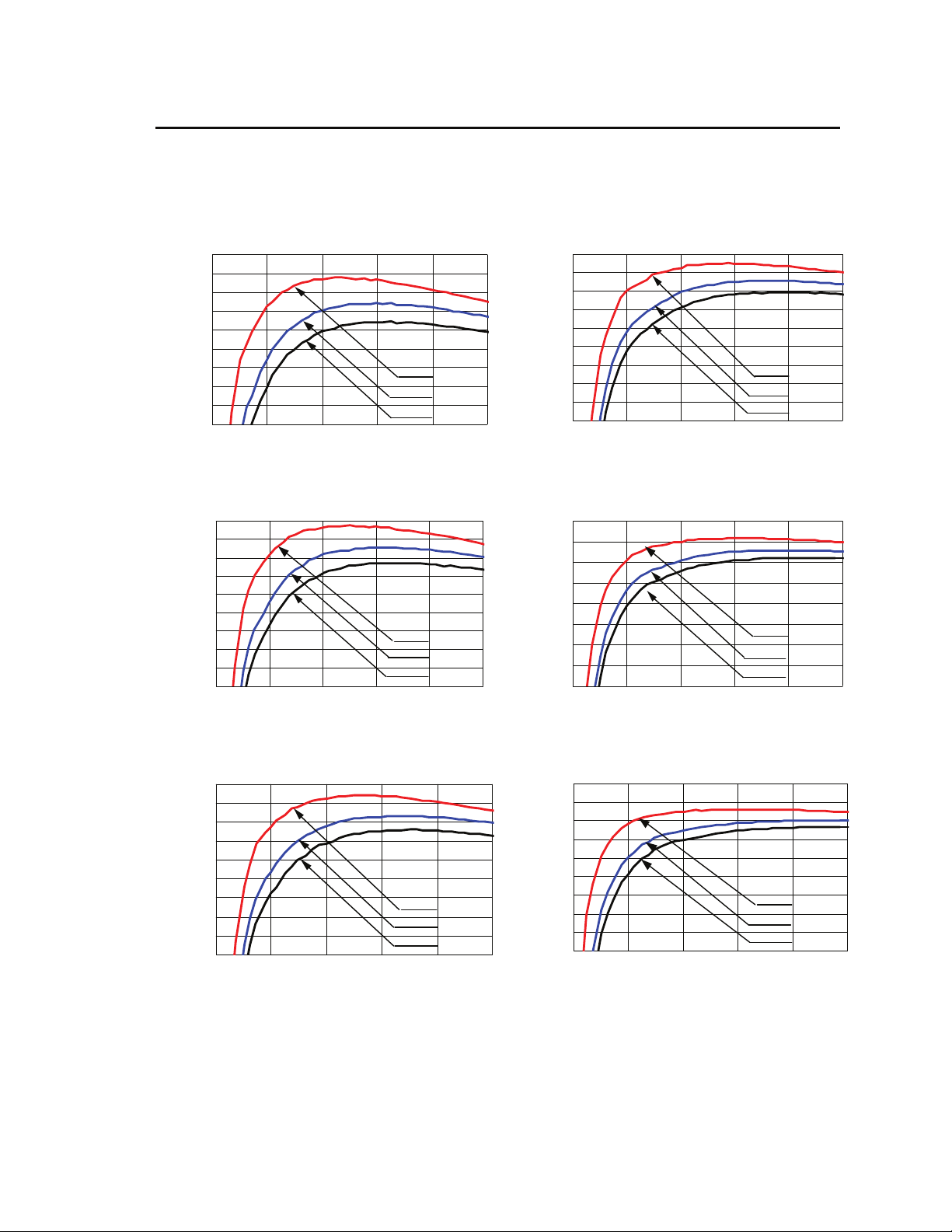
Characteristic Curves
The following figures provide typical characteristics for the Austin MiniLynxTM 12 V SIP modules at 25ºC.
88
86
84
82
80
78
76
74
72
EFFICIENCY, η (%)
70
0 0 .6 1.2 1.8 2 .4 3
VIN = 8.3V
VIN = 12.0V
VIN =14.0V
OUTPUT CURRENT, IO (A)
Figure 1. Converter Efficiency versus Output Current
(Vout = 1.2Vdc).
88
86
84
82
80
78
76
74
72
EFFICIENCY, η (%)
70
VIN = 8.3V
VIN = 12.0V
VIN= 14.0V
00.61.21.82.43
OUTPUT CURRENT, IO (A)
Figure 2. Converter Efficiency versus Output Current
(Vout = 1.5Vdc).
92
90
88
86
84
82
80
78
76
EFFICIENCY, η (%)
74
0 0.6 1.2 1.8 2 .4 3
OUTPUT CURRENT, IO (A)
Figure 4. Converter Efficiency versus Output Current
(Vout = 2.5Vdc).
95
92
89
86
83
80
77
74
EFFICIENCY, η (%)
71
0 0.6 1.2 1.8 2.4 3
OUTPUT CURRENT, IO (A)
Figure 5. Converter Efficiency versus Output Current
(Vout = 3.3Vdc).
VIN = 8.3V
VIN =12.0V
VIN= 14.0V
VIN = 8.3V
VIN = 12 .0V
VIN = 14 .0V
90
88
86
84
82
80
78
76
74
EFFICIENCY, η (%)
72
00.61.21.82.43
VIN = 8.3V
VIN = 12 .0V
VIN = 14 .0V
OUTPUT CURRENT, IO (A)
Figure 3. Converter Efficiency versus Output Current
(Vout = 1.8Vdc).
99
96
93
90
87
84
81
78
75
EFFICIENCY, η (%)
72
0 0 .6 1.2 1.8 2.4 3
VIN = 8.3V
VIN = 12 .0V
VIN =14.0V
OUTPUT CURRENT, IO (A)
Figure 6. Converter Efficiency versus Output Current
(Vout = 5.0Vdc).
LINEAGE POWER 6
Page 7

Data Sheet
(V)
October 2, 2009
Austin MiniLynx
8.3 – 14Vdc Input; 0.75Vdc to 5.5Vdc Output; 3A output current
TM
12V SIP Non-isolated Power Modules:
Characteristic Curves (continued)
The following figures provide typical characteristics for the Austin MiniLynxTM 12V SIP modules at 25ºC.
1. 6
1. 4
1. 2
(A)
IN
1
0.8
0.6
0.4
0.2
INPUT CURRENT, I
0
7 8 91011121314
Figure 7. Input voltage vs. Input Current
INPUT VOLTAGE, V
IN
(Vout =3.3Vdc).
Io=3 A
Io=1.5A
Io=0 A
(V) (200mV/div)
O
(A) (1A/div) V
O
OUTPUT CURRENT, OUTPUT VOLTAGE
I
TIME, t (5 μs/div)
Figure 10. Transient Response to Dynamic Load
Change from 50% to 100% of full load (Vo = 3.3Vdc).
(V) (10mV/div)
O
V
OUTPUT VOLTAGE
TIME, t (1μs/div)
Figure 8. Typical Output Ripple and Noise
IN = 12.0V dc, Vo = 0.75Vdc, Io=3A).
(V
(V) (10mV/div)
O
OUTPUT VOLTAGE
V
TIME, t (1μs/div)
Figure 9. Typical Output Ripple and Noise
(
VIN = 12.0V dc, Vo = 3.3Vdc, Io=3A).
(V) (200mV/div)
O
(A) (1A/div) V
O
OUTPUT CURRENT, OUTPUT VOLTAGE
I
TIME, t (5 μs/div)
Figure 11. Transient Response to Dynamic Load
Change from 100% to 50% of full load (Vo = 3.3 Vdc).
(V) (50mV/div)
O
(A) (1A/div) V
O
OUTPUT CURRENT, OUTPUT VOLTAGE
I
TIME, t (50μs/div)
Figure 12. Transient Response to Dynamic Load
Change from 50% to 100% of full load (Vo = 3.3 Vdc,
Cext = 2x150 μF Polymer Capacitors).
LINEAGE POWER 7
Page 8

Data Sheet
μ
(
October 2, 2009
Austin MiniLynx
8.3 – 14Vdc Input; 0.75Vdc to 5.5Vdc Output; 3A output current
TM
12V SIP Non-isolated Power Modules:
Characteristic Curves (continued)
The following figures provide typical characteristics for the Austin MiniLynxTM 12 V SIP modules at 25ºC.
(V) (1V/div)
(V) (50mV/div)
O
O
(A) (1A/div) V
O
OUTPUT CURRENT, OUTPUTVOLTAGE
I
TIME, t (50μs/div)
Figure 13. Transient Response to Dynamic Load
Change from 100% of 50% full load (Vo = 3.3Vdc, Cext
= 2x150
ON/OFF VOLTAGE OUTPUT VOLTAGE
F Polymer Capacitors).
(V) (1V/div)
O
(V) (10V/div) V
On/off
V
TIME, t (1ms/div)
Figure 14. Typical Start-Up Using Remote On/Off
(V
IN = 12.0Vdc, Vo = 3.3Vdc, Io = 3A).
(V) (1V/div)
O
(V) (10V/div) V
IN
INPUT VOLTAGE OUTPUT VOLTAGE
V
TIME, t (1ms/div)
Figure 16. Typical Start-Up with application of Vin
(V
IN = 12.0Vdc, Vo = 3.3Vdc, Io = 3A).
(V) (0.5V/div)
O
(V) (10V/div) V
On/off
V
ON/OFF VOLTAGE OUTPUT VOLTAGE
TIME, t (1ms/div)
Figure 17 Typical Start-Up Using Remote On/Off
with Prebias (V
IN = 12.0Vdc, Vo = 1.8Vdc, Io = 1.0A,
Vbias =1.0Vdc).
(A) (5A/div)
O
(V) (10V/div) V
On/off
V
ON/OFF VOLTAGE OUTPUT VOLTAGE
F
igure 15. Typical Start-Up Using Remote On/Off with
Low-ESR external capacitors (7x150uF Polymer)
TIME, t (1ms/div)
OUTPUT CURRENT,
I
TIME, t (20ms/div)
Figure 18. Output short circuit Current
IN = 12.0Vdc, Vo = 0.75Vdc).
(V
VIN = 12.0Vdc, Vo = 3.3Vdc, Io = 3A, Co = 1050μF).
LINEAGE POWER 8
Page 9

Data Sheet
October 2, 2009
Austin MiniLynx
8.3 – 14Vdc Input; 0.75Vdc to 5.5Vdc Output; 3A output current
TM
12V SIP Non-isolated Power Modules:
Characteristic Curves (continued)
The following figures provide thermal derating curves for the Austin MiniLynxTM 12 V SIP modules.
3.5
3
2.5
2
1. 5
1
0.5
0
OUTPUT CURRENT, Io (A)
100 LFM
0 LFM
20 30 40 50 60 70 80 90
AMBIENT TEMPERATURE, TA OC
Figure 19. Derating Output Current versus Local
Ambient Temperature and Airflow (V
Vo=0.75Vdc).
OUTPUT CURRENT, Io (A)
3.5
3.0
2.5
2.0
1. 5
1. 0
0.5
0.0
100 LFM
0 LFM
20 30 40 50 60 70 80 90
AMBIENT TEMPERATURE, TA OC
IN = 12.0 Vdc,
Figure 20. Derating Output Current versus Local
Ambient Temperature and Airflow (V
IN = 12.0Vdc,
Vo=1.8 Vdc).
3.5
3.0
2.5
2.0
1. 5
1. 0
0.5
0.0
OUTPUT CURRENT, Io (A)
100 LFM
0 LFM
20 30 40 50 60 70 80 90
AMBIENT TEMPERATURE, TA OC
Figure 21. Derating Output Current versus Local
Ambient Temperature and Airflow
(VIN = 12.0Vdc,
Vo=3.3 Vdc).
Figure 22. Derating Output Current versus Local
Ambient Temperature and Airflow (V
Vo=5.0 Vdc).
3.5
3.0
2.5
2.0
1. 5
1. 0
0.5
0.0
OUTPUT CURRENT, Io (A)
10 0 LF M
0 LFM
20 30 40 50 60 70 80 90
AMBIENT TEMPERATURE, TA OC
IN = 12 Vdc,
LINEAGE POWER 9
Page 10

Data Sheet
F
F
October 2, 2009
8.3 – 14Vdc Input; 0.75Vdc to 5.5Vdc Output; 3A output current
Austin MiniLynx
Test Configurations
TO OSCILLOSCOPE
L
TEST
1μH
CS 1000μF
BATTERY
NOTE: Measure input reflected ripple current with a simulated
Electrolytic
E.S.R.<0.1Ω
@ 20°C 100kHz
source induct anc e (L
possible battery impedance. Measure current as shown
above.
) of 1μH. Capacit or CS offsets
TEST
Figure 23. Input Reflected Ripple Current Test
Setup.
COPPER STRIP
V
(+)
O
1uF .
COM
GROUND PLANE
NOTE: All voltage measurements to be taken at the module
terminals, as shown above. If socket s are used then
Kelvin connections are required at the module terminals
to avoid measurement errors due to socket contact
resistance.
Figure 24. Output Ripple and Noise Test Setup.
R
R
contact
distribution
VIN(+)
V
IN
10uF
V
CIN
2x100μF
Tantalum
O
V
O
SCOPE
CURRENT PROBE
VIN(+)
COM
RESISTIVE
LOAD
R
contactRdistribution
R
LOAD
TM
12V SIP Non-isolated Power Modules:
Design Considerations
Input Filtering
Austin MiniLynxTM 12V SIP module should be
connected to a low -impedance source. A highly
inductive source can affect the stability of the module.
An input capacitance must be placed directly adjacent
to the input pin of the module, to minimize input ripple
voltage and ensure module stability in the presence of
inductive traces that supply input voltage to the
module.
In a typical application, a 22 µF low-ESR ceramic
capacitors will be sufficient to provide adequate ripple
voltage at the input of the module. To further
minimize ripple voltage at the input, additional
ceramic capacitors are recommended at the input of
the module. Figure 26 shows input ripple voltage
(mVp-p) for various outputs with a 10 µF or a 22µF
input ceramic capacitor at full load.
350
300
250
1 x 10u
1 x 22u
200
150
100
50
0
0.5 1 1.5 2 2.5 3 3.5 4 4.5 5 5.5
Figure 26. Input ripple voltage for various outputs
with 10 µF or a 22 µF ceramic capacitor at the
input (full-load).
R
R
contact
distribution
NOTE: All volt age meas urements to be taken at th e module
terminals , as shown above. If socket s are us ed then
Kelvin conn ections are requir ed at the modu le termi nals
to avoid measur ement err ors due to soc ket contact
resistance.
COM
COM
R
contactRdistribution
Figure 25. Output Voltage and Efficiency Test
Setup.
. I
V
O
Efficiency
=
η
VIN. I
O
IN
x 100 %
LINEAGE POWER 10
Page 11

Data Sheet
October 2, 2009
8.3 – 14Vdc Input; 0.75Vdc to 5.5Vdc Output; 3A output current
Austin MiniLynx
Design Considerations (continued)
Output Filtering
The Austin MiniLynxTM 12 V SIP module is designed
for low output ripple voltage and will meet the
maximum output ripple specification with 1 µF
ceramic and 10 µF tantalum capacitors at the output
of the module. However, additional output filtering
may be required by the system designer for a number
of reasons. First, there may be a need to further
reduce the output ripple and noise of the module.
Second, the dynamic response characteristics may
need to be customized to a particular load step
change.
To reduce the output ripple and improve the dynamic
response to a step load change, additional
capacitance at the output can be used. Low ESR
polymer and ceramic capacitors are recommended to
improve the dynamic response of the module. For
stable operation of the module, limit the capacitance
to less than the maximum output capacitance as
specified in the electrical specification table.
TM
12V SIP Non-isolated Power Modules:
Safety Considerations
For safety agency approval the power module must
be installed in compliance with the spacing and
separation requirements of the end-use safety agency
standards, i.e., UL 60950-1, CSA C22.2 No. 60950-103, and VDE 0850:2001-12 (EN60950-1) Licensed.
For the converter output to be considered meeting the
requirements of safety extra-low voltage (SELV), the
input must meet SELV requirements. The power
module has extra-low voltage (ELV) outputs when all
inputs are ELV.
The input to these units is to be provided with a fastacting fuse with a maximum rating of 6A in the
positive input lead
.
LINEAGE POWER 11
Page 12

Data Sheet
October 2, 2009
8.3 – 14Vdc Input; 0.75Vdc to 5.5Vdc Output; 3A output current
Austin MiniLynx
Feature Description
Remote On/Off
Austin MiniLynxTM 12V SIP power modules feature an
On/Off pin for remote On/Off operation. Two On/Off
logic options are available in the Austin MiniLynx
12V series modules. Positive Logic On/Off signal,
device code suffix “4”, turns the module ON during a
logic High on the On/Off pin and turns the module
OFF during a logic Low. Negative logic On/Off signal,
no device code suffix, turns the module OFF during
logic High and turns the module ON during logic Low.
For positive logic modules, the circuit configuration for
using the On/Off pin is shown in Figure 27. The
On/Off pin is an open collector/drain logic input signal
(Von/Off) that is referenced to ground. During a logichigh (On/Off pin is pulled high internal to the module)
when the transistor Q1 is in the Off state, the power
module is ON. Maximum allowable leakage current of
the transistor when Von/off = V
IN,max
is 10µA.
Applying a logic-low when the transistor Q1 is turnedOn, the power module is OFF. During this state
VOn/Off must be less than 0.3V. When not using
positive logic On/off pin, leave the pin unconnected or
tie to V
I
ON/OFF
GND
IN.
VIN+
ON/OFF
V
ON/OFF
Q1
MODULE
R2
+
_
R1
Q2
PWM Enable
R3
R4
Figure 27. Circuit configuration for using positive
logic On/OFF.
For negative logic On/Off devices, the circuit
configuration is shown is Figure 28. The On/Off pin is
pulled high with an external pull-up resistor (typical
pull-up = 68k, +/- 5%). When transistor Q1 is in the
R
Off state, logic High is applied to the On/Off pin and
the power module is Off. The minimum On/off voltage
for logic High on the On/Off pin is 2.5 Vdc. To turn
the module ON, logic Low is applied to the On/Off pin
by turning ON Q1. When not using the negative logic
On/Off, leave the pin unconnected or tie to GND.
TM
Q3 CSS
TM
12V SIP Non-isolated Power Modules:
VIN+
ON/OFF
GND
R
pull-up
I
ON/OFF
V
ON/OFF
Q1
+
_
MODULE
PWM Enable
R1
Q2 CSS
R2
Figure 28. Circuit configuration for using
negative logic On/OFF.
Overcurrent Protection
To provide protection in a fault (output overload)
condition, the unit is equipped with internal
current-limiting circuitry and can endure current
limiting continuously. At the point of current-limit
inception, the unit enters hiccup mode. The unit
operates normally once the output current is brought
back into its specified range. The typical average
output current during hiccup is 3.5A.
Input Undervoltage Lockout
At input voltages below the input undervoltage lockout
limit, module operation is disabled. The module will
begin to operate at an input voltage above the
undervoltage lockout turn-on threshold.
Overtemperature Protection
To provide over temperature protection in a fault
condition, the unit relies upon the thermal protection
feature of the controller IC. The unit will shutdown if
the thermal reference point T
exceeds 140
o
C (typical), but the thermal shutdown is
, (see Figure 31)
ref2
not intended as a guarantee that the unit will survive
temperatures beyond its rating. The module will
automatically restarts after it cools down.
LINEAGE POWER 12
Page 13

Data Sheet
October 2, 2009
8.3 – 14Vdc Input; 0.75Vdc to 5.5Vdc Output; 3A output current
Austin MiniLynx
Feature Descriptions (continued)
Output Voltage Programming
The output voltage of the Austin MiniLynx
be programmed to any voltage from 0.75Vdc to
5.5Vdc by connecting a resistor (shown as Rtrim in
Figure 29) between Trim and GND pins of the
module. Without an external resistor between Trim
and GND pins, the output of the module will be
0.7525Vdc. To calculate the value of the trim resistor,
Rtrim for a desired output voltage, use the following
equation:
10500
Rtrim
⎢
−
Vo
⎣
⎡
= 1000
−
7525.0
Rtrim is the external resistor in Ω
Vo is the desired output voltage
For example, to program the output voltage of the
Austin MiniLynx
TM
12V module to 1.8V, Rtrim is
calculated as follows:
10500
⎡
= 1000
Rtrim
⎢
−
7525.08.1
⎣
V
V
(+)
IN
(+)
O
TM
12V can
⎤
Ω
⎥
⎦
⎤
−
⎥
⎦
Ω= kRtrim 024.9
TM
12V SIP Non-isolated Power Modules:
Using 1% tolerance trim resistor, set point tolerance
of ±2% is achieved as specified in the electrical
specification. The POL Programming Tool, available
at www.lineagepower.com under the Design Tools
section, helps determine the required external trim
resistor needed for a specific output voltage.
Voltage Margining
Output voltage margining can be implemented in the
Austin MiniLynx
R
margin-up
margining-up the output voltage and by connecting a
resistor, R
pin for margining-down. Figure 30 shows the circuit
configuration for output voltage margining. The POL
Programming Tool, available at
www.lineagepower.com under the Design Tools
section, also calculates the values of R
R
margin-down
Please consult your local Lineage Power technical
representative for additional details.
TM
modules by connecting a resistor,
, from the Trim pin to the ground pin for
margin-down
, from the Trim pin to the Output
and
margin-up
for a specific output voltage and % margin.
Vo
Rmargin-down
Austin Lynx or
Lynx II Series
Q2
Trim
Rmargin-up
ON/OFF
TRIM
R
trim
GND
Figure 29. Circuit configuration to program
output voltage using an external resistor.
Table 1 provides Rtrim values required for some
LOAD
Rtrim
Q1
GND
Figure 30. Circuit Configuration for margining
Output voltage.
common output voltages.
Table 1
V
(V) Rtrim (KΩ)
O, set
0.7525 Open
1.2 22.46
1.5 13.05
1.8 9.024
2.5 5.009
3.3 3.122
5.0 1.472
LINEAGE POWER 13
Page 14

Data Sheet
A
W
October 2, 2009
8.3 – 14Vdc Input; 0.75Vdc to 5.5Vdc Output; 3A output current
Austin MiniLynx
Thermal Considerations
Power modules operate in a variety of thermal
environments; however, sufficient cooling should be
provided to help ensure reliable operation.
Considerations include ambient temperature, airflow,
module power dissipation, and the need for increased
reliability. A reduction in the operating temperature of
the module will result in an increase in reliability. The
thermal data presented here is based on physical
measurements taken in a wind tunnel. The test setup is shown in Figure 32. Note that the airflow is
parallel to the long axis of the module as shown in
figure 31. The derating data applies to airflow in
either direction of the module’s long axis.
Airflow
TM
12V SIP Non-isolated Power Modules:
25.4_
(1.0)
76.2_
(3.0)
ind Tun ne l
PWBs
x
5.97_
(0.235)
ir
flow
Po w e r M od u le
Probe Location
for measuring
airflow and
ambient
temperature
Tref1
Tref2
Figure 31. T
location.
The thermal reference point, T
specifications is shown in Figure 32. For reliable
operation this temperature should not exceed 115
The output power of the module should not exceed
the rated power of the module (Vo,set x Io,max).
Please refer to the Application Note “Thermal
Characterization Process For Open-Frame BoardMounted Power Modules” for a detailed discussion of
thermal aspects including maximum device
temperatures.
Temperature measurement
ref
used in the
ref
o
C.
Figure 32. Thermal Test Set-up.
Heat Transfer via Convection
Increased airflow over the module enhances the heat
transfer via convection. Thermal derating curves
showing the maximum output current that can be
delivered by various module versus local ambient
temperature (T
0.5m/s (100 ft./min) are shown in the Characteristics
Curves section.
) for natural convection and up to
A
LINEAGE POWER 14
Page 15

Data Sheet
October 2, 2009
8.3 – 14Vdc Input; 0.75Vdc to 5.5Vdc Output; 3A output current
Austin MiniLynx
Post solder Cleaning and Drying
Considerations
Post solder cleaning is usually the final circuit-board
assembly process prior to electrical board testing. The
result of inadequate cleaning and drying can affect
both the reliability of a power module and the
testability of the finished circuit-board assembly. For
guidance on appropriate soldering, cleaning and
drying procedures, refer to Board Mounted Power
Modules: Soldering and Cleaning Application Note.
Through-Hole Lead-Free Soldering
Information
The RoHS-compliant through-hole products use the
SAC (Sn/Ag/Cu) Pb-free solder and RoHScompliant components. They are designed to be
processed through single or dual wave soldering
machines. The pins have an RoHS-compliant
finish that is compatible with both Pb and Pb-free
wave soldering processes. A maximum preheat
rate of 3°C/s is suggested. The wave preheat
process should be such that the temperature of the
power module board is kept below 210°C. For Pb
solder, the recommended pot temperature is
260°C, while the Pb-free solder pot is 270°C max.
Not all RoHS-compliant through-hole products can
be processed with paste-through-hole Pb or Pbfree reflow process. If additional information is
needed, please consult with your Lineage Power
technical representative for more details.
TM
12V SIP Non-isolated Power Modules:
LINEAGE POWER 15
Page 16

Data Sheet
October 2, 2009
Austin MiniLynx
8.3 – 14Vdc Input; 0.75Vdc to 5.5Vdc Output; 3A output current
TM
12V SIP Non-isolated Power Modules:
Mechanical Outline
Dimensions are in millimeters and (inches).
Tolerances: x.x mm ± 0.5 mm (x.xx in. ± 0.02 in.) [unless otherwise indicated]
x.xx mm ± 0.25 mm (x.xxx in ± 0.010 in.)
Top View
Side View
PIN FUNCTION
1 Vo
2 Trim
3 GND
4 VIN
5 On/Off
LINEAGE POWER 16
Page 17

Data Sheet
October 2, 2009
Austin MiniLynx
8.3 – 14Vdc Input; 0.75Vdc to 5.5Vdc Output; 3A output current
TM
12V SIP Non-isolated Power Modules:
Recommended Pad Layout
Dimensions are in millimeters and (inches).
Tolerances: x.x mm ± 0.5 mm (x.xx in. ± 0.02 in.) [unless otherwise indicated]
x.xx mm ± 0.25 mm (x.xxx in ± 0.010 in.)
PIN FUNCTION
1 Vo
2 Trim
3 GND
4 VIN
5 On/Off
LINEAGE POWER 17
Page 18

Data Sheet
a
©
October 2, 2009
Austin MiniLynx
8.3 – 14Vdc Input; 0.75Vdc to 5.5Vdc Output; 3A output current
TM
12V SIP Non-isolated Power Modules:
Ordering Information
Please contact your Lineage Power Sales Representative for pricing, availability and optional features.
Table 2. Device Codes
Device Code
Input
Voltage
AXA003A0X 8.3 – 14Vdc 0.75 – 5.5Vdc 3 A 91.0% SIP
AXA003A0XZ 8.3 – 14Vdc
AXA003A0X4 8.3 – 14Vdc
AXA003A0X4Z 8.3 – 14Vdc
-Z refers to RoHS compliant Versions
Output
Voltage
0.75 – 5.5Vdc
0.75 – 5.5Vdc
0.75 – 5.5Vdc
Output
Current
Efficiency
3.3V@ 3A
3 A 91.0%
3 A 91.0%
3 A 91.0%
Connector
Type
SIP
SIP
SIP
Comcodes
108992624
CC109101268
108992632
CC109104824
Asia-Pacific Headquarters
Tel: + 65 6593 7211
World Wide Headquarters
Lineage Power Corporation
601 Shil oh Roa d, Plano, TX 75074, USA
+1-800-526-7 819
(Outsi de U.S.A.: +1-972-244-9428)
www.lineagepower.com
e-mail: techs upport1@lineagepower.com
Linea ge Power res erves th e right to make change s to the prod uct(s) or i nformation c ontained herein without not ic e. No liability is ass umed as a result o f their use o r
pplication . No righ ts under any patent accompany the sal e of any s uch produc t(s) or informati on.
Linea ge Power D C-DC pro ducts are p rotected unde r v arious pa tents. Infor mation on these pa tents is av ailable at ww w.line agepower .com/paten ts.
2009 Line age Power Corporation, (Plan o, Texas) All Inte rn ation al Rights Reserved.
Europe, Middle-East and Africa Headquarters
Tel: + 49 898 780 672 80
India Headquarters
Tel: + 91 80 2841163 3
LINEAGE POWER 18
Document No: DS04-041 ver. 1.32
PDF name: minilynx_sip_12v_ds.pdf
 Loading...