

Page 1

19” LCD Color Monitor Gateway FPD1965
1
Service
Service
Service
TABLE OF CONTENTS
Description Page Description Page
N
SAFETY NOTICE
ANY PERSON ATTEMPTING TO SERVICE THIS CHASSIS MUST FAMILIARIZE HIMSELF WITH THE
CHASSIS AND BE AWARE OF THE NECESSARY SAFETY PRECAUTIONS TO BE USED WHEN SERVICING
ELECTRONIC EQUIPMENT CONTAINING HIGH VOLTAGES.
Table Of Contents.......……..……..........................…........1
Revision List.….............……..........................……......2
Important Safety Notice.…………....................……......3
1. Monitor Specification..............................………........4
2. LCD Monitor Description…………………………….......5
3. Operation Instruction…………...............……...........6
3.1 General Instructions...........................…...........6
3.2 Control Button…………….…..............……...............6
3.3 Adjusting the Picture...........................…............7
4. Input/Output Specification............……………............10
4.1 Input Signal Connector............………….................10
4.2 Factory Preset Display Modes.........................11
4.3 Panel Specification.....………………..................11
5. Block Diagram……...................…………................14
5.1 Soft Flow Chart….………………..…………....….......14
5.2 Electrical Block Diagram….……………..….......16
6.Schematic……………....................................…18
6.1 Main Board.……...……..........................................18
6.2 Power Board..………..……....................................23
7.PCB Layout..……………….......................................25
7.1 Main Board…………….........................................25
7.2 Power Board…..………...................................26
7.3 Keypad Board………….....................................26
8. Maintainability……….......................................27
8.1 Equipments and Tools Requirement……..............27
8.2 Trouble Shooting…….………..............................28
9. White-Balance, Luminance adjustment.............34
10. Monitor Exploded View……….…………… ...........35
11. BOM List……….....................................................36
12.Different Parts List……………………………………76
CAUTION: USE A SEPARATE ISOLATION TRANSFOMER FOR THIS UNIT WHEN SERVICING
Page 2

19” LCD Color Monitor Gateway FPD1965
2
Revision List
Revision Date Revision History TPV Model
A00 Jun-2-06 Initial Release T980KKCHKGGKNP
A01 Mar.-27-07 Add TPV Model in item11 T95KGCHKDPGKNC
A02 May.-14-07 Add TPV Model in item11 T97KGCHKDPGKN
A03 May.-14-07 Add TPV Model In Item 12 T97KGCHKDPGYNC
A04 Jun.-27-07 Add TPV Model In Item 12 T97HGCHKDPYENC
Page 3

19” LCD Color Monitor Gateway FPD1965
3
Important Safety Notice
Proper service and repair is important to the safe, reliable operation of all AOC Company Equipment. The service
procedures recommended by AOC and described in this service manual are effective methods of performing service
operations. Some of these service operations require the use of tools specially designed for the purpose. The
special tools should be used when and as recommended.
It is important to note that this manual contains various CAUTIONS and NOTICES which should be carefully read in
order to minimize the risk of personal injury to service personnel. The possibility exists that improper service
methods may damage the equipment. It is also important to understand that these CAUTIONS and NOTICES ARE
NOT EXHAUSTIVE. AOC could not possibly know, evaluate and advise the service trade of all conceivable ways in
which service might be done or of the possible hazardous consequences of each way. Consequently, AOC has not
undertaken any such broad evaluation. Accordingly, a servicer who uses a service procedure or tool which is not
recommended by AOC must first satisfy himself thoroughly that neither his safety nor the safe operation of the
equipment will be jeopardized by the service method selected.
Hereafter throughout this manual, AOC Company will be referred to as AOC.
WARNING
Use of substitute replacement parts, which do not have the same, specified safety characteristics may create shock,
fire, or other hazards.
Under no circumstances should the original design be modified or altered without written permission from AOC.
AOC assumes no liability, express or implied, arising out of any unauthorized modification of design.
Servicer assumes all liability.
FOR PRODUCTS CONTAINING LASER:
DANGER-Invisible laser radiation when open AVOID DIRECT EXPOSURE TO BEAM.
CAUTION-Use of controls or adjustments or performance of procedures other than those specified herein may
result in hazardous radiation exposure.
CAUTION -The use of optical instruments with this product will increase eye hazard.
TO ENSURE THE CONTINUED RELIABILITY OF THIS PRODUCT, USE ONLY ORIGINAL MANUFACTURER'S
REPLACEMENT PARTS, WHICH ARE LISTED WITH THEIR PART NUMBERS IN THE PARTS LIST SECTION OF
THIS SERVICE MANUAL.
Take care during handling the LCD module with backlight unit
-Must mount the module using mounting holes arranged in four corners.
-Do not press on the panel, edge of the frame strongly or electric shock as this will result in damage to the screen.
-Do not scratch or press on the panel with any sharp objects, such as pencil or pen as this may result in damage to
the panel.
-Protect the module from the ESD as it may damage the electronic circuit (C-MOS).
-Make certain that treatment person’s body is grounded through wristband.
-Do not leave the module in high temperature and in areas of high humidity for a long time.
-Avoid contact with water as it may a short circuit within the module.
-If the surface of panel becomes dirty, please wipe it off with a soft material. (Cleaning with a dirty or rough cloth may
damage the panel.)
Page 4
19” LCD Color Monitor Gateway FPD1965
4
1. Monitor Specifications
Item Description
Driving system TFT Color LCD
Type HT190E01-100
Size 48.0cm(19.0")
Pixel pitch 0.294mm(H) x 0.294mm(V)
Viewable angle (CR>10) 150˚ (H) 135˚ (V) (type)
LCD Panel
Response time 8ms (type)
Sync. Type H/V TTL
15Pin Analog
Input Signal
24Pin Digital
Analog: 30kHz – 83kHz
H-Frequency
Digital: 30kHz-71kHz
Analog: 56Hz-75Hz
Input
V-Frequency
Digital: 56Hz-75Hz
ON Mode: <40W
Power Consumption
OFF Mode: <1W
Analog: 135MHz (Max)
Dot Clock
Digital: 108MHz (Max)
Contrast Ratio 700:1
White Luminance 300cd/m
2
Max. Resolution 1280 x 1024
Plug & Play VESA DDC2BTM
Power Source 90~264VAC,47~63Hz
Display Color 16.2M colors
Active area Horizontal: 376.32mm; Vertical: 301.06mm
Environmental
Considerations
Operating Temp: 10°C to 35°C
Storage Temp: -20°C to 60°C
Operating Humidity: 5% to 90%
Page 5
19” LCD Color Monitor Gateway FPD1965
5
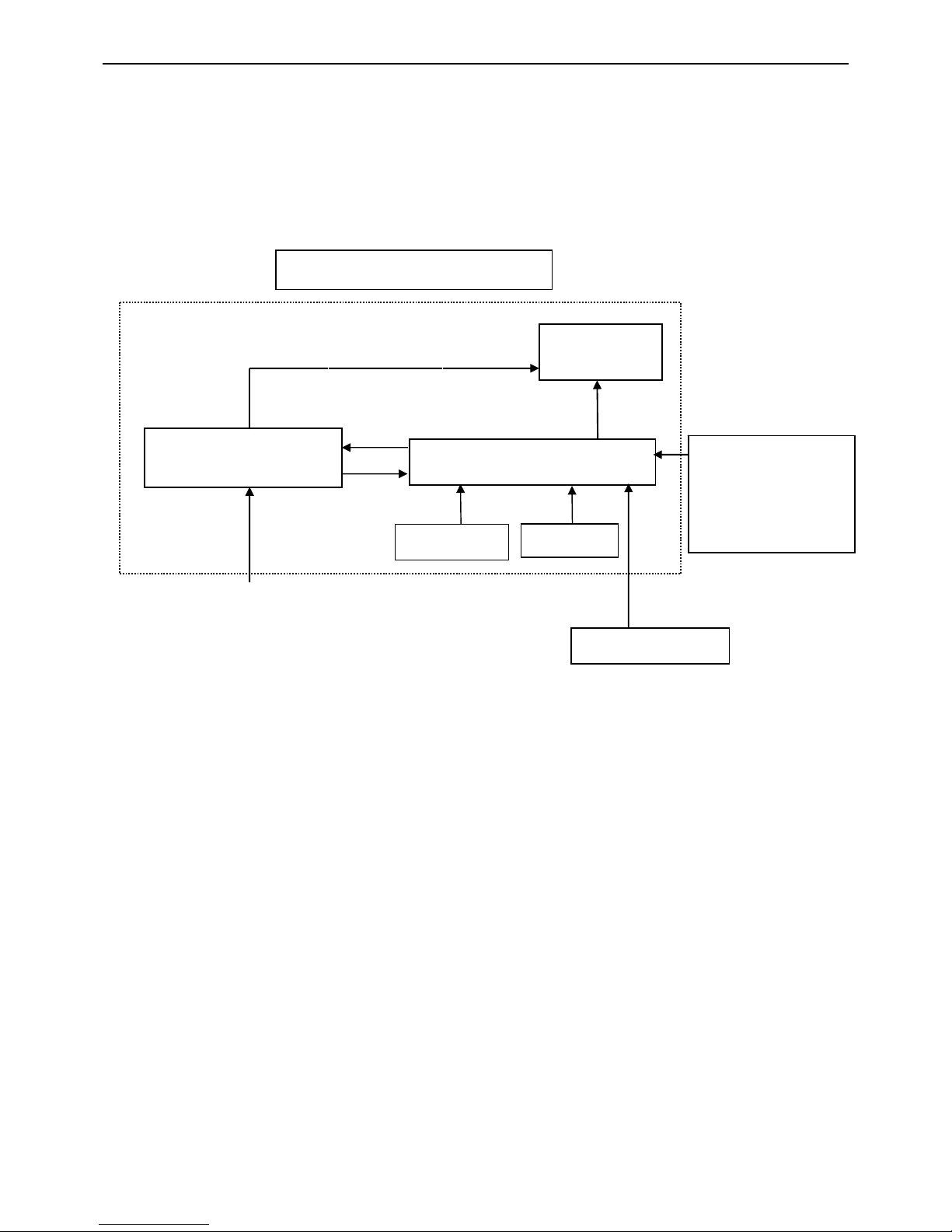
2. LCD Monitor Description
The LCD MONITOR will contain a main board, a power board and two keypad boards which house the flat panel
control logic, brightness control logic and DDC.
The power board will provide AC to DC Inverter voltage to drive the backlight of panel and the main board chips
each voltage.
HOST Computer
AC-IN
100V-240V
PWPC board
(
Include: adapter, inverter)
Flat Panel and
CCFL backlight
Main Board
RS232 Connector
For white balance
adjustment in factory
mode
CCFL Drive.
Video signal,
Monitor Block Diagram
Keyboard
Keyboard
Page 6
19” LCD Color Monitor Gateway FPD1965
6
3. Operating Instructions
3.1 General Instructions
Press the power button to turn the monitor on or off. The other control buttons are located in the side of the
monitor. By changing these settings, the picture can be adjusted to your personal preferences.
-
The power cord should be connected.
-
Connect the video cable from the monitor to the video card.
-
Press the power button to turn on the monitor, the power indicator will light up.
3.2 Control Buttons
- Power Button:
When pressed, the monitor enters the off mode, and the LED turns blank. Press again to restore normal status.
- Left / Right Button:
The Left/Right Button is used to control the monitor functions. Press to switch functions or adjust settings.
- Auto Adjust Key:
The Auto Adjust Key is used to automatically set the H Position, V Position, Clock and Phase.
- Power Indicator:
Blue — Power On mode.
Orange — Power Saving mode.
Blank —Power Off Mode.
NO. Name
Within OSD
Without OSD
1 Input Back to previous menu Select input signal: Analog or Digital
2
Auto
Select Function or enter Sub menu
Auto configuration
3 / ▲
1.Move the cursor up
2.Increase the value of the selected item
Activate the Brightness menu
4
/ ▼
1.Move the cursor down
2.Decrease the value of the selected item
Activate the contrast menu
5 MENU Exit the OSD menu Activate the OSD menu
6 POWER Power On / Off Power On / Off
①
②
③
④
⑤
⑥
Page 7
19” LCD Color Monitor Gateway FPD1965
7
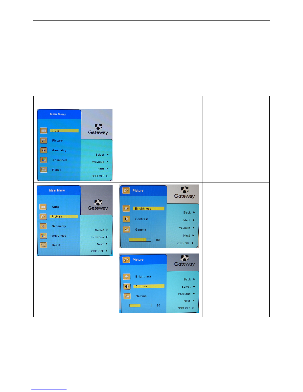
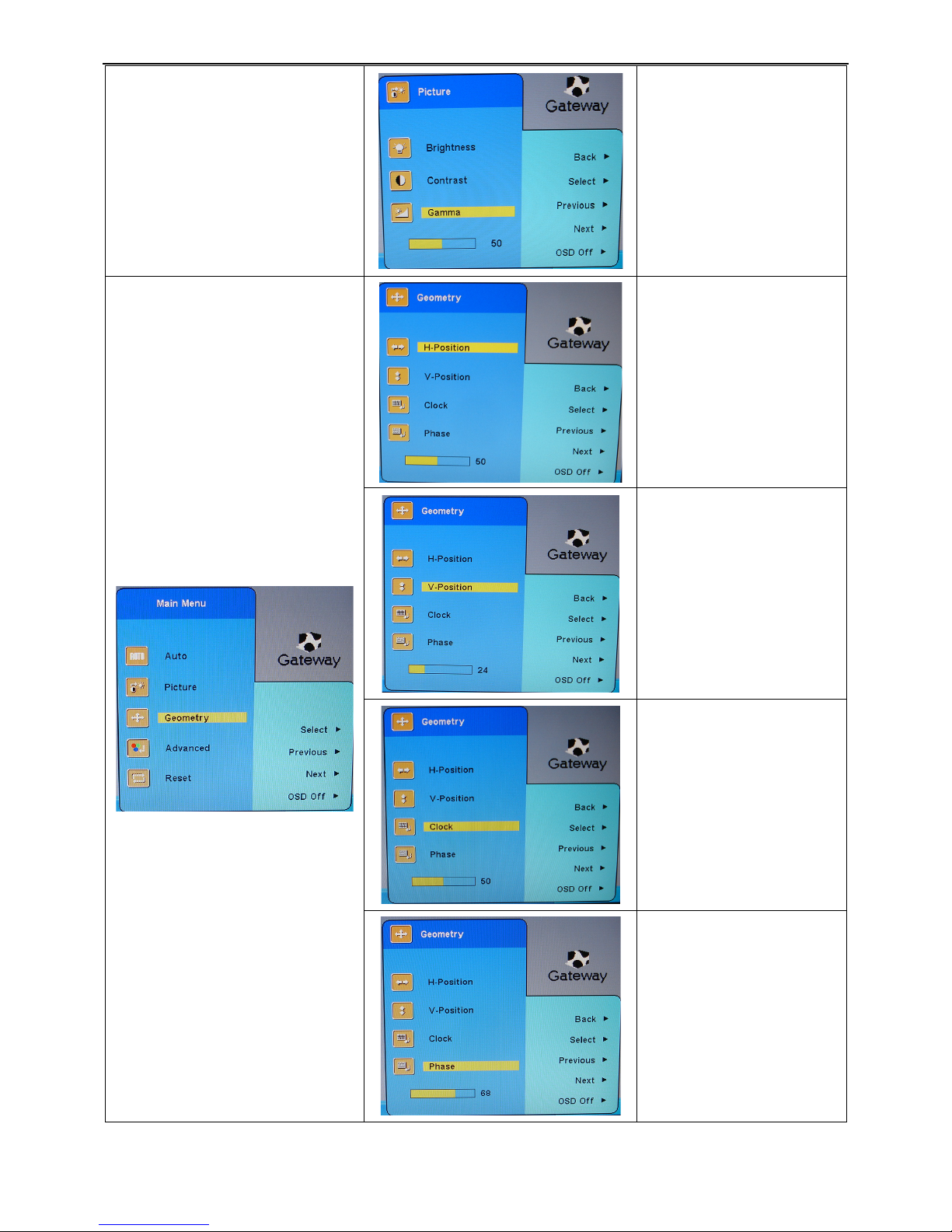
3.3 Adjusting The Picture
Adjustment steps:
1. Press the MENU-button to activate the OSD window.
2. Press < or > to select the desired function.
3. Press the MENU-button to select the function that you want to adjust.
4. Press < or > to change the settings of the current function.
5. To exit and save, select the exit function, or leave the monitor alone for 10 seconds. If you want to adjust any
other function, repeat steps 2-4.
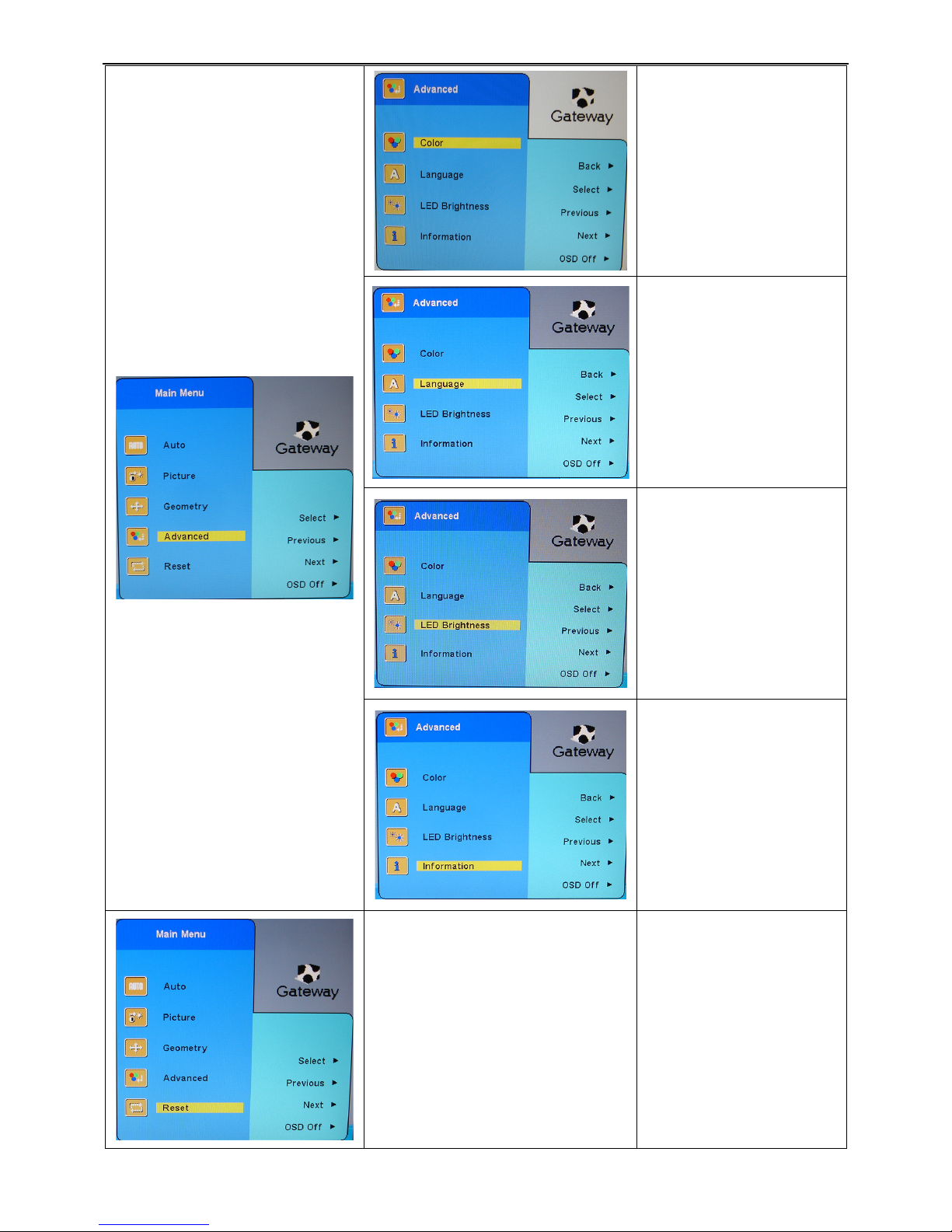
Main Menu Sub Menu Description
N/A Auto adjustment
Brightness adjustment
Contrast adjustment
Page 8
19” LCD Color Monitor Gateway FPD1965
8
Gamma adjustment
Moves the display image left
and right.
Moves the display image up
and down.
Adjust picture Clock to reduce
Vertical-Line noise.
Adjust Picture Phase to
reduce Horizontal-Line noise.
Page 9
19” LCD Color Monitor Gateway FPD1965
9
Customizes the color levels.
Change the language of the
OSD.
Change LED Brightness
modes between Day Mode
and Nite Mode.
Displays screen resolution,
the current input mode, and
the OSD version.
N/A
Resets the monitor to its
factory settings.
Page 10
19” LCD Color Monitor Gateway FPD1965
10
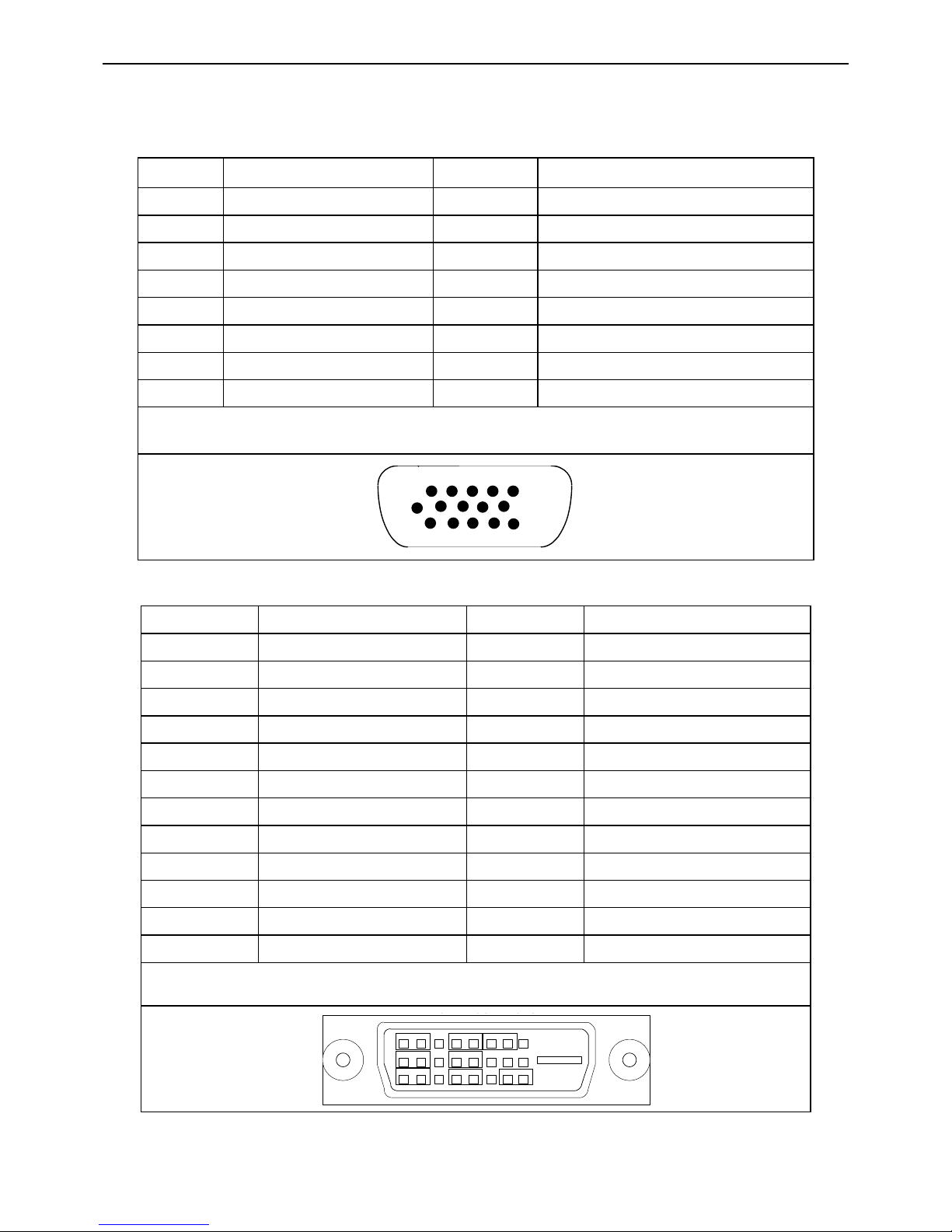
4. Input/Output Specification
4.1 Input Signal Connector
1. D-SUB connector
Pin No. Description Pin No. Description
1. Red Video 9. No Pin!
2. Green Video 10. Ground
3. Blue Video 11. Ground
4. Ground 12. DDC-Serial Data
5. DDC-Return 13. H-Sync
6. Red Ground 14. V-Sync
7. Green Return 15. DDC-Serial Clock
8. Blue Return
Analog Connector
12345
10
12
11
6
13
14
15
2. DVI connector
Pin No. Description Pin No. Description
1.
TMDS data 2-
13.
TMDS data 3+
2.
TMDS data 2+
14.
+5V Power
3. TMDS data 2/4 Shield 15. GND (for +5V)
4.
TMDS data 4-
16. Hot Plug Detect
5.
TMDS data 4+
17.
TMDS data 0-
6. DDC Clock 18.
TMDS data 0+
7. DDC Data 19. TMDS data 0/5 Shield
8. No Connect 20.
TMDS data 5-
9.
TMDS data 1-
21.
TMDS data 5+
10.
TMDS data 1+
22. TMDS Clock Shield
11. TMDS data 1/3 Shield 23. TMDS Clock +
12.
TMDS data 3-
24.
TMDS Clock -
Digital Connector
GCOCO
9 10 11
TMDS Data 1
+
-
19
SHLD 1/3
SHLD 0/5
1 2 3
TMDS Data 2
+-
SHLD 2/4
4 5
TMDS Data 2
+-
12 13 14
TMDS Data 3
+
-
20 21 22
TMDS Data 5
+
-
15816
NO
CONNECT
HOT PLUG
DETECT
+5V
GND
CLOCK
SHLD
23 24
TMDS CLOCK
-+
6 7
CLK
DATA
DDC
TMDS Data 0
18+17
-
Page 11
19” LCD Color Monitor Gateway FPD1965
11
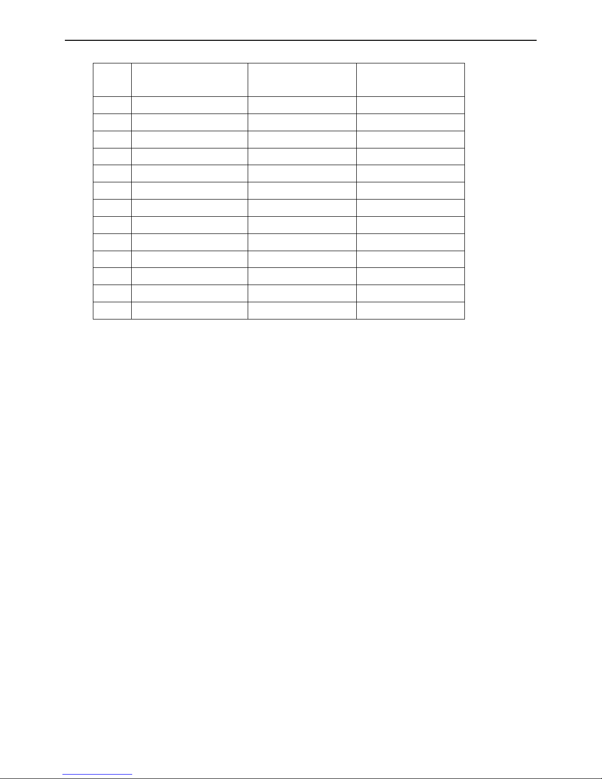
4.2 Factory Preset Display Modes
No
Mode name and
Resolution
Hor. Frequency (KHz) Vt. Frequency (Hz)
1 VGA 720x400 31.469 70.087
2 VGA 640x480 31.469 59.941
3 VESA 640x480 37.861 72.810
4 VESA 640x480 37.500 75.000
5 VESA 800x600 35.156 56.250
6 VESA 800x600 37.879 60.317
7 VESA 800x600 48.077 72.188
8 VESA 800x600 46.875 75.000
9 VESA 1024x768 48.363 60.004
10 VESA 1024x768 56.476 70.069
11 VESA 1024x768 60.023 75.029
12 VESA 1280x1024 63.980 60.020
13 VESA 1280x1024 79.976 75.025
Page 12
19” LCD Color Monitor Gateway FPD1965
12
4.3 Panel Specification
4.3.1 Features
4.3.2 Display Characteristics
Page 13
19” LCD Color Monitor Gateway FPD1965
13
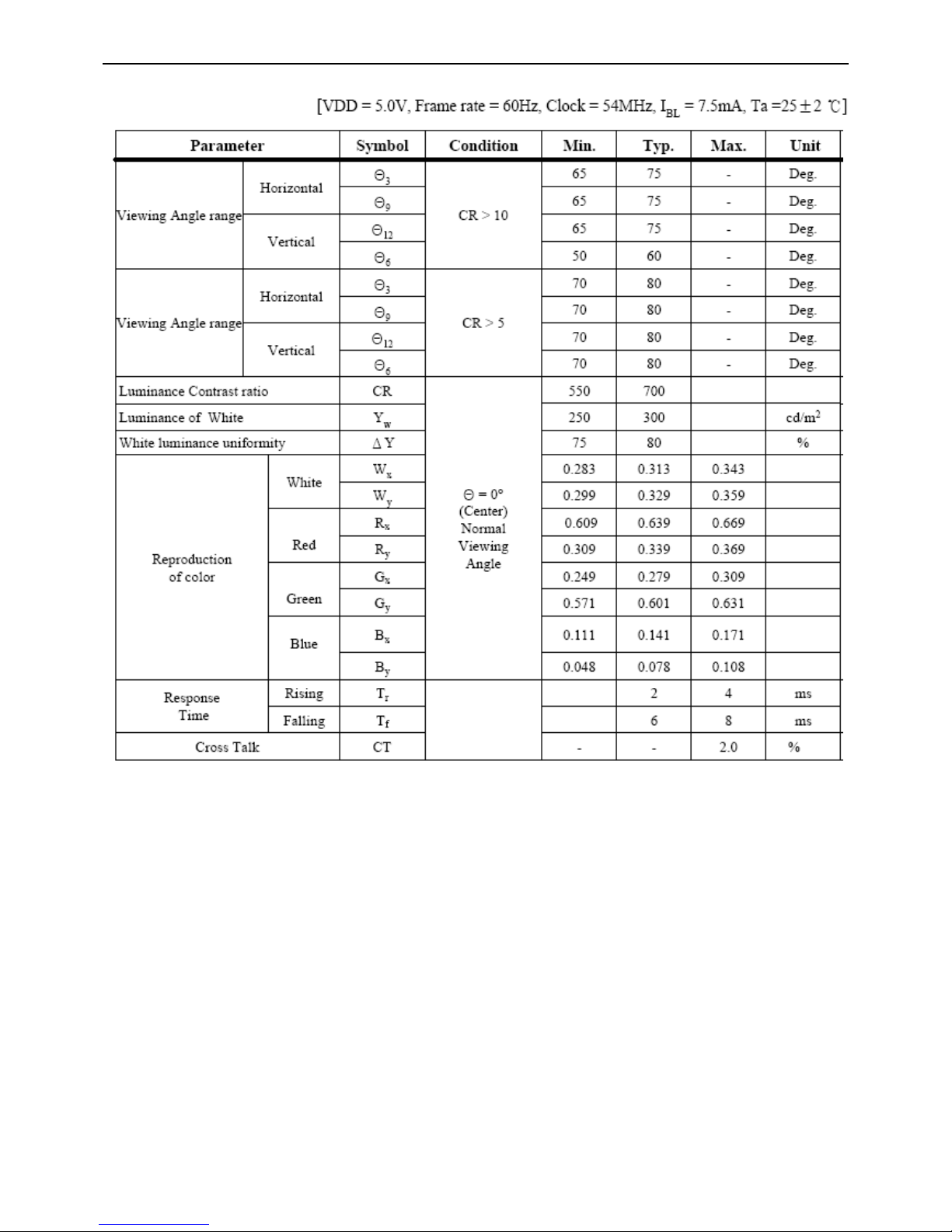
4.3.3 Optical Characteristics
Page 14
19” LCD Color Monitor Gateway FPD1965
14
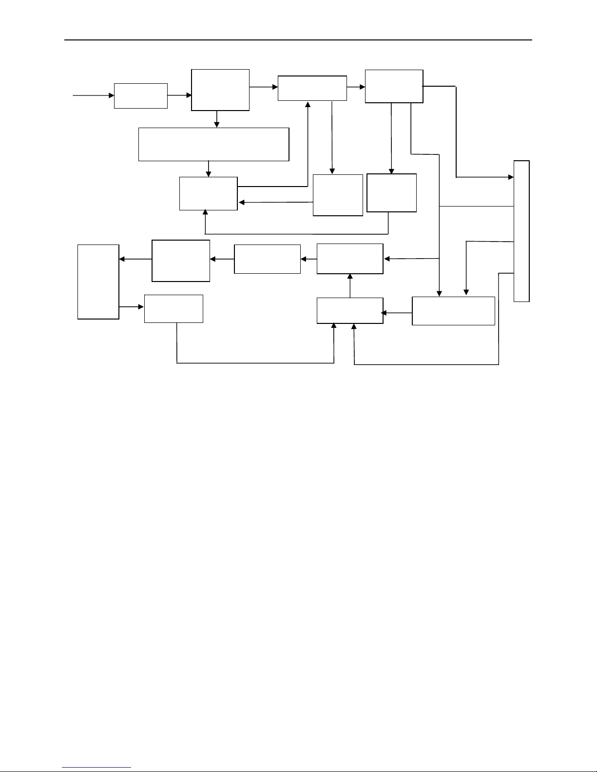
5. Block Diagram
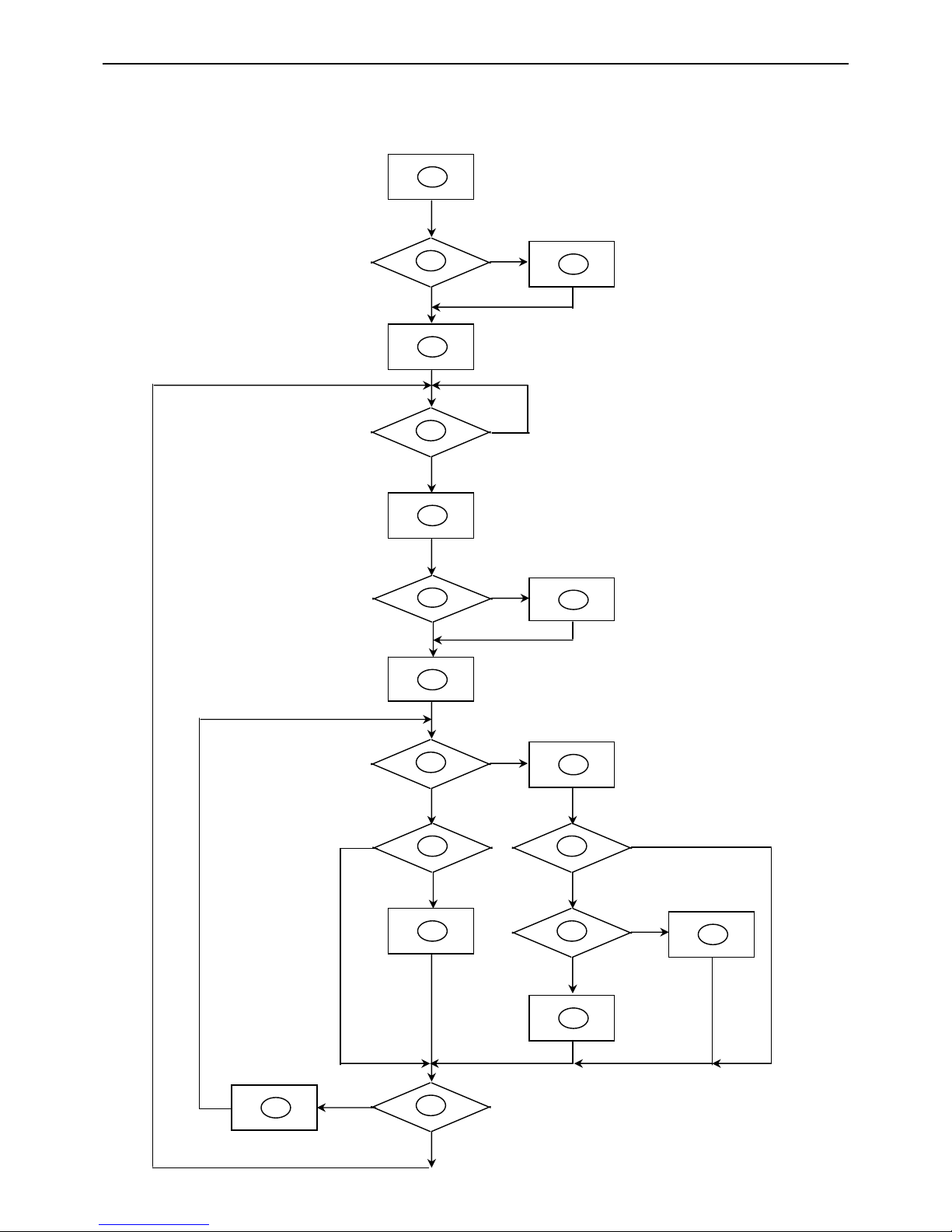
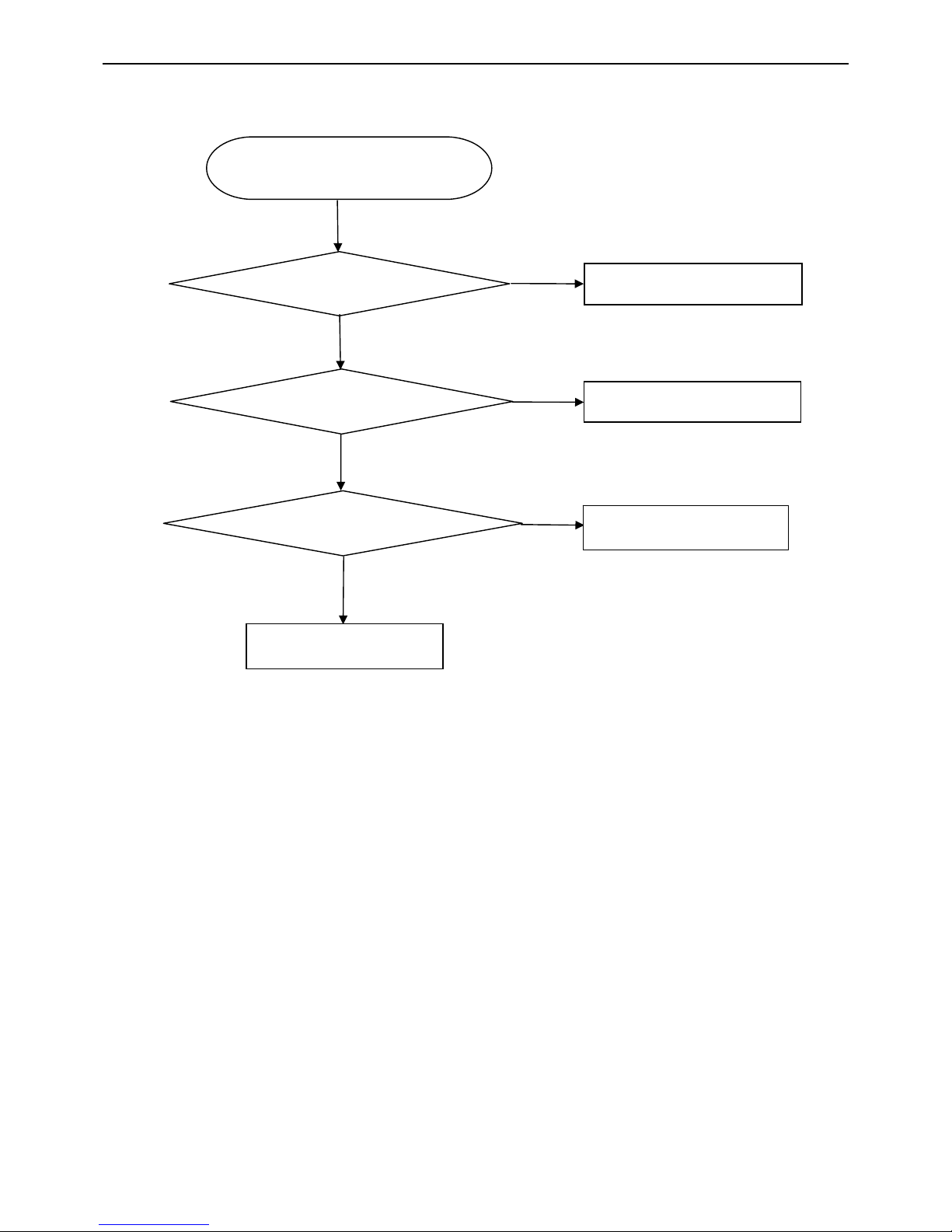
5.1 Software Flow Chart
1
2
N
Y
5
Y
N
10
Y
N
12
Y
N
7
N
6
4
3
9
14
11
13
Y
N
15
Y
N
16
17
19
Y
N
18
Page 15

19” LCD Color Monitor Gateway FPD1965
15
1) MCU initializes.
2) Is the EPROM blank?
3) Program the EPROM by default values.
4) Get the PWM value of brightness from EPROM.
5) Is the power key pressed?
6) Clear all global flags.
7) Are the AUTO and SELECT keys pressed?
8) Enter factory mode.
9) Save the power key status into EPROM.
Turn on the LED and set it to green color.
Scalar initializes.
10) In standby mode?
11) Update the lifetime of back light.
12) Check the analog port, are there any signals coming?
13) Does the scalar send out an interrupt request?
14) Wake up the scalar.
15) Are there any signals coming from analog port?
16) Display "No connection Check Signal Cable" message. And go into standby mode after the message
disappears.
17) Program the scalar to be able to show the coming mode.
18) Process the OSD display.
19) Read the keyboard. Is the power key pressed?
Page 16
19” LCD Color Monitor Gateway FPD1965
16
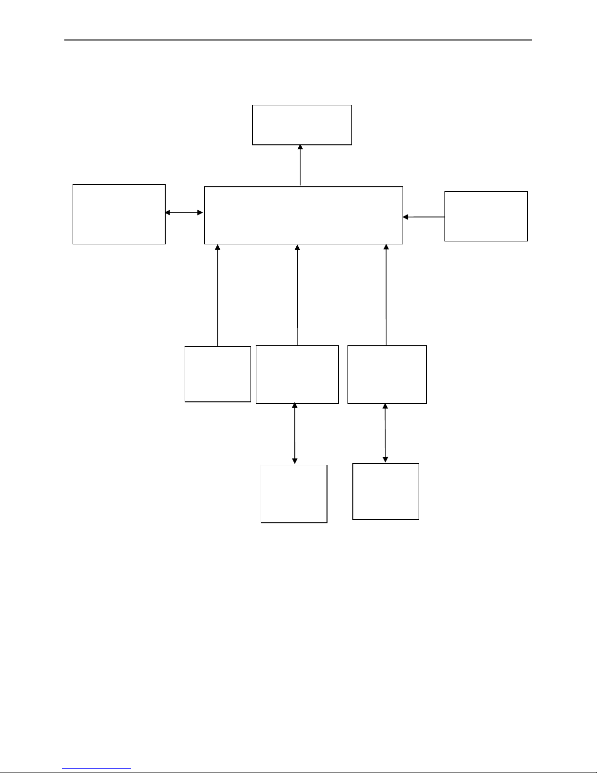
5.2 Electrical Block Diagram
5.2.1 Main Board
Flash Memory
SST25VF010
(U402)
Scalar IC GM 5621-LF-AA
(Include MCU, ADC, OSD)
(U401)
D-Sub
Connector
(CN202)
EEPROM
24C02
(U202)
H sync
V sync
RGB
DB15_SDA,
DB15
_
SCL
LCD Interface
(CN501)
DVI-I only
Connector
(CN201)
EEPROM
24C02
(U201)
D_H sync
D_V sync
D_RGB
OSD Control
Interface
(CN402)
Crystal
14.318MHZ
(X301)
Page 17
19” LCD Color Monitor Gateway FPD1965
17
5.2.2 Inverter/Power Board
CN902
EMI filter
Bridge
Rectifier
and Filter
Start Circuit: R909、R910、 R931
PWM
Control IC
Transformer
Over
Voltage
Protect
Rectifier
diodes
AC input
12V
ON/OFF Control
PWM
Control IC
Feedback
Circuit
Output
Circuit
Transformer
MOSFET
Q805、Q806
Lamp
ON/OFF
DIM
PWM
Feedback
Circuit
12V
5V
Page 18

19” LCD Color Monitor Gateway FPD1965
18
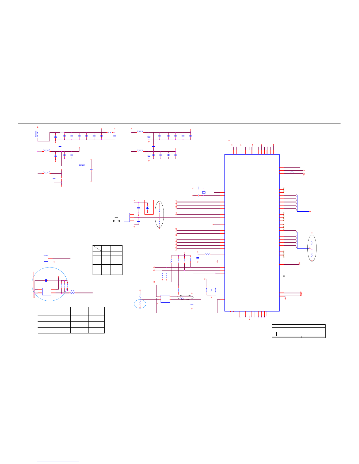
6. Schematic
6.1 Main Board
715G1691- 1
+5V
R215 220 1/16W
RXC- (3)
R217 22K 1/16W
C212
0.047uF
FB202
60 OHM
GND
R223 75 1/16W
+3.3V_VDD
VGA_PLUG
CN202
DB15
1
6
2
7
3
8
4
9
5
11
12
13
14
15
10
1716
2005.05.20 FOR NMV Issue
ED107
SG168
VGA_5V
DDC_SCL_VGA(3)
R220 75 1/16W
R206 10 1/16W
GND
GND
RX1- (3)
R238 220 1/16W
GND
VS_IN
SDA_IN
2
DVI_EDID_WP (3)
RX2- (3)
GND
RX1-IN
R209 10 1/16W
DDC_SDA_A
ED104
SG168
DDC_SDA_VGA(3)
D209
BAV70
3
1
2
C209
0.1uF/16V
U201
M24C02WMN6
1
2
3
4 5
6
7
8
A0
A1
A2
VSS SDA
SCL
WC
VCC
Q201
2N7002E
3D
1
G
2
S
GND
+5V
GND
Bin
C218
NC
C214
0.1uF/16V
D211
BAV99
3
1
2
R202 10 1/16W
DDC_SCL_DVI (3)
ED103
SG168
R240
2.2K 1/16W
+5V
R239 220 1/16W
GREEN- (3)
DVI_HPD
RX0+ (3)
GND
RXC-IN
D212
BAV99
3
1
2
RED+ (3)
SCL_IN
ED101
SG168
R205 10 1/16W
C217
NC
C215
0.047uF
RX2+ (3)
CABLE_DET (3)
ZD212
UDZS5.6B
FB204
430 OHM
FB203
60 OHM
C222
0.1uF/16V
(8 mil)
R203 10 1/16W
RX2+IN
ED108
SG168
ZD208
UDZS5.6B
ZD213
UDZS5.6B
+5V
GND
R212
4.7K 1/16W
R234
75 1/16W
R243 0 1/16W
ZD215
UDZS5.6B
BLUE+ (3)
R201 10K 1/16W
GND
ZD202
UDZS5.6B
Pins 6/7/8 are R/G/B
return lines resp.
BLUE- (3)
GND
R218 33K 1/16W
SDA_IN
Gin
(10 mil,
┰キ︽絬
)
C216
0.047uF
RX2-IN
R229 75 1/16W
R213
4.7K 1/16W
U202
M24C02WMN6
4
81
237
6
5
GND
VCCA0
A1A2WP
SCL
SDA
1
FB201
60 OHM
R241
2.2K 1/16W
DVI_HPD
VS (3)
CN201
JACK
1
2
3
4
5
6
7
8
9
10
11
12
13
14
15
17
18
19
20
21
23
24
C1
16
22
C2
C3
C4
C5
25
26
T2T2+
SGND
T4-
T4+
DDCCLK
DDCDAT
A_VSYNC
T1-
T1+
SGND
T3-
T3+
+5V
GND
T0-
T0+
SGND
T5-
T5+
TC+
TC-
A_RED
HPD
SGND
A_GREEN
A_BLUE
A_HSYNC
A_GND
A_GND
A_GND
R216 220 1/16W
R222 100 1/16W
0522 ESD SOLUTION
A
Input Connectors
C
26Tuesday, November 08, 2005
Title
Size Document Number Rev
Date: Sheet
of
ZD203
UDZS5.6B
ED106
SG168
GND
+5V
AGND
HS (3)
R207 10 1/16W
C210
0.047uF
RED- (3)
RXC+IN
R233
75 1/16W
C201
1000pF
ZD201
UDZS5.6B
GREEN+ (3)
ZD211
UDZS5.6B
RX1+IN
RX0+IN
R226
4.7K 1/16W
GND
C213
0.047uF
R224 100 1/16W
+5V
AGND
GND
R204 10 1/16W
HOT_PLUG
+5V
R214
10K 1/16W
ZD204
UDZS5.6B
ZD214
UDZS5.6B
VGA_PLUG
HS_in
R211
10K 1/16W
ZD207
UDZS5.6B
SCL_IN
RX0-IN
3
D213
BAV99
3
1
2
C221
0.1uF/16V
D210
BAV70
3
1
2
C219
0.1uF/16V
R208 10 1/16W
ED105
SG168
C211
0.047uF
Rin
RX0- (3)
ZD209
UDZS5.6B
R210 220 1/16W
ED102
SG168
0522 ESD SOLUTION
DVI_5V
GND
R230 100 1/16W
R232 220 1/16W
R227
4.7K 1/16W
GND
GND
2005/04/22 Write protect
R235
75 1/16W
R228 220 1/16W
R242
10K 1/16W
C220
0.1uF/16V
RX1+ (3)
DDC_SCL_A
GND
DVI_5V
VGA_5V
RXC+ (3)
ZD210
UDZS5.6B
GND
GND
DDC_SDA_DVI (3)
R237 220 1/16W
75-ohm terminating resistor
very close to the VGA
conn.
Page 19
19” LCD Color Monitor Gateway FPD1965
19
L301
120 OHM
(PWM1)
Standard SPI ROM
GND
C307
0.1uF/16V
3.3V_PVDD
1.8V_DVDD
GM5621 GM2621BC
3.3V_DDC
/WP
+3.3V_VDD
R317
4.7K 1/16W
LVDS_E5
NVRAM_SCL
DDC_SDA_DVI(2)
R312
4.7K 1/16W
C313
0.1uF/16V
Open
Ext. ROM JTAG Off
C321
0.1uF/16V
2
CONTROL GM2621
R323
4.7K 1/16W
R316
4.7K 1/16W
C335
0.1uF/16V
Close to respective power Pins
R329
GND
GND
BLUE-(2)
R313
NC
C334
0.1uF/16V
C324
0.1uF/16V
C328 33pF
RX2+(2)
/WP
RESETn
LVDS_O5
LED_TR(4)
LVDS_E[0..9]
R313
1.8V_AVDD
1
GND
RXC+(2)
R331 0 1/16W
GND
GND
3.3V_AVDD
LVDS_E4
C332
0.1uF/16V
LVDS_E1
R307
4.7K 1/16W
R314
GND
6.2K
3.3V_PVDD
R312
3.3V_AVDD
3.3V_DVDD
LVDS_E6
UDART_DO
R308
4.7K 1/16W
Standard SPI ROM
L303
120 OHM
U403
M24C16-MN6T
1
2
3
4 5
6
7
8
A0
A1
A2
VSS SDA
SCL
WC
VCC
3.3V_LAVDD
Open
PPWR (6)
Close to respective power Pins
UART on GPO
1.8V_AVDD
RED+(2)
UDART_DO
ROM_WP#
ZD301
UDZS5.6B
R325
NC
R319
NC
LVDS_O4
+
C301
22uF
R303
NC
Remove ROM_WP# function to GPIO12
3.3V_DVDD
U401
56
49
50
33
34
36
37
38
39
35
29
40
62
60
27
45
41
96
42
119
100
61
12
10
9
8
5
4
3
24
6
7
94
93
52
127
125
124
123
46
44
43
51
28
32
31
30
13
14
15
16
85
19
20
21
22
11
23
99
59
97
103
104
105
106
108
109
110
111
89
90
65
64
121
120
122
126
128
57
58
63
66
67
69
72
73
75
76
80
81
83
84
107
112
113
114
115
12648
1755118
87
9598102
91
116
53
10192827422547
687177
79
867870
185488
117
GPO_1
PBIAS
PWM0 / GP0_4
O_CLK_N
O_CLK_P
O_CH2_P
O_CH1_N
O_CH1_P
O_CH0_N
O_CH2_N
RESERVED
O_CH0_P
SPI_DO
SPI_CLK
RESERVED
RESERVED
RESERVED
GREEN+
RESERVED
PWM1 / GPO_5
RED-
SPI_DI
E_CH2_P
E_CLK_P
E_CLK_N
E_CH3_P
RESERVED
RESERVED
RESERVED
RESERVED
RESERVED
E_CH3_N
BLUE-
BLUE+
CRVSS
PPWR
GPIO_13
GPIO_12
GPIO_11
RESERVED
RESERVED
RESERVED
GPO_0
RESERVED
O_CH3_P
O_CH3_N
RESERVED
E_CH1_N
E_CH1_P
E_CH0_N
E_CH0_P
AVSS_DVI
RESERVED
RESERVED
RESERVED
RESERVED
E_CH2_N
RESERVED
RED+
SPI_CSn
GREEN-
AVSS_ADC
AVDD_ADC_18
VBUFC_RPLL
VDD_RPLL_18
XTAL
TCLK
AVDD_RPLL_33
RESETn
HSYNC
VSYNC
DDC_SDA_VGA
DDC_SCL_VGA
GPIO_9
GPIO_8
GPIO_10
GPIO_14
AVDD_BIAS_33
GPO_2
GPO_3
RESERVED
DDC_SCL_DVI
DDC_SDA_DVI
REXT
RX2+
RX2RX1+
RX1RX0+
RX0RXC+
RXC-
VSS_RPLL
LBADC_VSS
LBADC_IN3
LBADC_IN2
LBADC_IN1
AVSS_BIAS
VSS_OUT
VSS_OUT
CVDD_18
CVDD_18
CVDD_18
CVDD_18
AVSS_ADC
AVSS_ADC
AVSS_ADC
RVDD_33
LBADC_VDD_33
RVDD_33
AVDD_ADC_33
AVDD_ADC_33
AVDD_DVI_33
AVDD_DVI_33
VDD_OUT_33
VDD_OUT_33
VDD_OUT_33
AVSS_DVI
AVSS_DVI
AVSS_DVI
AVSS_DVI
AVDD_DVI_18
AVDD_DVI_18
AVDD_DVI_18
CRVSS
CRVSS
CRVSS
CRVSS
Boot-Strap Configuration:
3.3V_DVDD
NVRAM_SDA
L305
120 OHM
ATMEL_EN
NVRAM_SCL
+3.3V_VDD
LVDS_O8
R304
NC
Open
G-PROBE
Move ROM_WP# function to GPIO12
CN301
CONN
1
2
3
RX1+(2)
NC
L304
120 OHM
GND
LVDS_O[0..9]
PBIAS
L302
120 OHM
AUDIO_STDBY(4)
C314
0.1uF/16V
GPO_0
DDC_SDA_VGA(2)
R302 249 1/16W
10 KOhm
POWER_ON (4)
LVDS_E9
R301 10 1/16W
OPTIONAL
FOR
DEBUGGING
PURPOSES
ONLY
GND
0522
BOM
LOSE
LVDS_O[0..9] (5)
R329
NC
NC
BRIGHTNESS(6)
A
gm5621
C
16Tuesday, November 08, 2005
Title
Size Document Number Rev
Date: Sheet
of
C333
0.1uF/16V
+
C309
22uF
R305
4.7K 1/16W
GND
C323
0.1uF/16V
C306
0.1uF/16V
R314
NC
Reseerver GM2621 BC Version
GND
NVRAM_SDA
3.3V_PVDD
NC
GND
C317
0.1uF/16V
X301
14.318MHz
GND
GND
LVDS_E[0..9] (5)
3
(PWM0)
GND
RESETn
LBADC1 (4)
12K
LVDS_O7
LVDS_O0
+
C316
22uF
U302
G691L400T73
3
2
1
VCC
RSTN
GND
1K
DDC_SCL_VGA(2)
NC
GND
LED_O (4)
L306
120 OHM
DVI_EDID_WP(2)
LVDS_O3
UDART_DI
ROM_WP#
LVDS_E3
Default
GND
C326
0.1uF/16V
ATMELSPI ROM
3.3V_AVDD
LVDS_E0
R319
NC
U402
SST25VF010-20-4C-SA
1
2
3
4 5
6
7
8
CE#
SO
WP#
VSS SI
SCK
HOLD#
VDD
LVDS_E8
R315
4.7K 1/16W
Reserver GM2621 BC Version LVDS
GND
RX2-(2)
Internal reset ciriuit mount R313=4.7K
+5V
C320
0.1uF/16V
R310 100 1/16W
GREEN-(2)
PBIAS (6)
ROM_SDI
LVDS_E2
R324
4.7K 1/16W
PPWR
R330
10K 1/16W
3.3V_PVDD
RX0-(2)
+3.3V_VDD
3.3V_DVDD
C302
0.1uF/16V
ATMELSPI ROM
GND
V_EDID_ATMEL
GND
3.3V_DVDD
LVDS_O1
C303
0.1uF/16V
UDART_DI
C327 33pF
GM5621
C308
0.1uF/16V
Internal reset circuit mount R319=12K,R314=6.2K
+
C319
22uF
1.8V_DVDD
GND
3.3V_RVDD
C310
0.1uF/16V
+5V
LBADC2 (4)
R306
4.7K 1/16W
C311
0.1uF/16V
Open
NC
C329
0.01uF
+1.8V_VDD
ROM_SCLK
GND
RX0+(2)
UART on DDC
Cancel this circuit
DDC_SCL_DVI(2)
C322
0.1uF/16V
RED-(2)
R321
R309 100 1/16W
RXC-(2)
C331
0.1uF/16V
C330
0.1uF/16V
C312
0.1uF/16V
(SPI_CSn)
0522 ESD SOLUTION
HS(2)
C305
0.1uF/16V
C318
0.1uF/16V
NC
3.3V_LAVDD
4.7K
VS(2)
R318
4.7K 1/16W
Name
RX1-(2)
LED_B (4)
UART_PIN_SEL
LVDS_O2
LVDS_O9
+
C325
22uF
GND
LVDS_O6
R311 100 1/16W
BLUE+(2)
GREEN+(2)
CABLE_DET (2)
LVDS_E7
C304
0.1uF/16V
Page 20
19” LCD Color Monitor Gateway FPD1965
20
+3.3V
KEY_LEFT
L404 300 OHM
C404
1000pF
C416
0.001uF
L401 300 OHM
C421
1000pF
+3.3V_VDD
R414 220 1/16W
VER D Modify led circuit.8-22
+3.3V_VDD
L405 300 OHM
R413 220 1/16W
+5V
C411
0.001uF
C407
1000pF
KEY_ONOFF
GND
+3.3V
LBADC1(3)
Q404
PMBS3906
GND
ZD401UDZS5.6B
GND
KEYPAD
B
46Tuesday, November 08, 2005
Title
Size Document Number Rev
Date: Sheet
of
GND
GND
KEY_INFO
Q403
PMBS3906
R428 Change 47K key R Change 1%
VER D Modify led circuit.8-22
CN401
CONN
1 2
3 4
5 6
7 8
9 10
11 12
13 14
R419 30K 1/16W
R405
47K 1/16W
POWER_ON(3)
R430
10K 1/16W
GND
+3.3V
ZD405
UDZS5.6B
C417
NC
KEY_LEFT
C409
1uF/25V
GND
GND
GND
C405
1000pF
09-14 ESD
SOLUTION
LED LIGHT CONTROL
7-11
GND
LED_TR(3)
LED_O
C401
NC
R410 47K 1/16W
R426 10K 1/16W
C402
NC
KEY_MENU
R402
4.7K 1/16W
KEY_AUTO
R407
150 1/16W
C415
0.001uF
GND
GND
R429
0 1/16W
C420
1000pF
MUTE
ZD406
UDZS5.6B
GND
C412
0.001uF
Q402
PMBS3904
GND
LED_ORANGE
C413
0.001uF
R424 4.7K 1/16W
AUDIO_STDBY (3)
KEY_MENU
R406
47K 1/16W
LED_Blue
R420 22K 1/16W
R415 220 1/16W
GND
LED_B
C408
0.1uF/16V
ESD Soluction 0630
GND
R418
10K 1/16W
R425 100 1/16W
+5V
GND
LBADC2(3)
STANDBY
R432
220 1/16W
R428 47K 1/16W
KEY_RIGHT
ADD KEY_INFO 6-27
KEY_INFO
KEY_AUTO
GNDGND
C414
0.001uF
R431
10K 1/16W
R417
10K 1/16W
+12V
GND
ZD402UDZS5.6B
R403 NC
L402 300 OHM
GND
GND
LED_B(3)
C410
1uF/25V
C406
1000pF
R412 220 1/16W
R427
100 1/16W
D401
BAV99
3
1
2
KEY_ONOFF
L403 300 OHM
KEY_RIGHT
CN402
CON16A
1 2
3 4
5 6
7 8
9 10
11 12
13 14
15 16
R411 220 1/16W
ADD KEY_INFO 6-27
LED_O (3)
R401
NC
GND
GND
R408
150 1/16W
R416
10K 1/16W
R421 22K 1/16W
ZD403UDZS5.6B
NOT USE -Gateway project
(audio function)
R422 30K 1/16W
ZD404
UDZS5.6B
GND
Q401
PMBS3906
+5V
R409 47K 1/16W
Page 21
19” LCD Color Monitor Gateway FPD1965
21
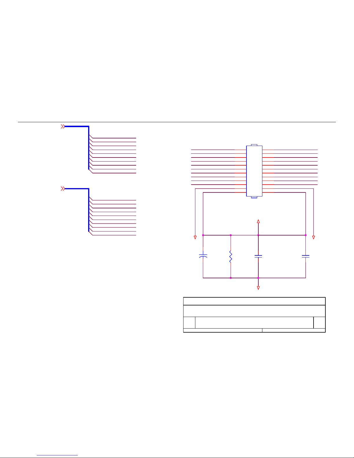
RXO2- LVDS_O5
LVDS_E2
LVDS_E3
RXE3-
LVDS_O6
RXO2+
RXE0-
LVDS_O1
RXO3+
RXO3-
A
PANEL INTERFACE
A
56Tuesday, November 08, 2005
Title
Size Document Number Rev
Date: Sheet
of
+VLCD
LVDS_O9
LVDS_E0
LVDS_O7
RXE1+
LVDS_E5
LVDS_O3
LVDS_E5
+
C501
22uF
RXE2RXEC-
RXE3+
LVDS_O7
LVDS_E8
LVDS_O1
RXE0+
RXOC+
CN501
CONN
2
4
6
8
10
12
14
16
18
20
22
24
1
3
5
7
9
11
13
15
17
19
21
23
LVDS_O[0..9](3)
LVDS_E2
LVDS_E1
RXO1-
LVDS_E9
LVDS_O3
C503
NC
RXE2+
LVDS_E3
LVDS_O4
LVDS_E7
LVDS_E0
LVDS_O6
LVDS_E[0..9](3)
LVDS_E6
LVDS_E7
LVDS_O4
GND
LVDS_E8
R501
1K 1/16W
LVDS_O0
LVDS_O9
LVDS_E9
GND
LVDS_E6
LVDS_O0
LVDS_O5
LVDS_O2
LVDS_O8
RXO1+
C502
0.1uF/16V
LVDS_E1
RXE1-
LVDS_O2
LVDS_E4
RXOC-
GND
RXO0+
RXO0-
15.4mA
RXEC+
LVDS_E4
LVDS_O8
Page 22
19” LCD Color Monitor Gateway FPD1965
22
BRIGHTNESS(3)
R610
NC
VCC5V
A
POWER
B
16Tuesday, November 08, 2005
Title
Size Document Number Rev
Date: Sheet
of
R602
1K 1/16W
ON_OFF
1.435A
+
C601
220uF/25V
+5V
C613
0.1uF/16V
Q602
AO3401
1
3
2
GND
CN601
CON402(PITCH 2.00)
1
3
5
7
9
11
2
4
6
8
10
12
C616
1uF/16V
0.8A-max
R609
47K 1/16W
GND
FB605
0 OHM
FB602
300 OHM
R608
47K 1/16W
VCC12V
0522 Inrush Solution
+5V
PBIAS (3)
GND
D601
FA20-04
GNDFB603
300 OHM
C607
0.1uF/16V
+12V
C608
0.1uF/16V
C614
1uF/16V
+
C615
22uF
+3.3V_VDD
GND
+VLCD
GND
+3.3V_VDD
GND
GND
+5V
+5V
PPWR(3)
C618
0.068uF/16V
GND
204mA
GND
Cancel C618,Add C617 1UF for
17"HSD and 19"HSD panel
+
C602
220uF/25V
+12V
+1.8V_VDD
+
C605
220uF/25V
+5V
GND
+5V
VCC5V
+
C609
NC
GND
+
C610
22uF
FB601
300 OHM
R601 4.7K 1/16W
+
C606
220uF/25V
VCC12V
R604
1K 1/16W
C612
0.1uF/16V
GND
C617
NC
Add C616
C604
0.1uF/16V
GND
Add C609 22UF for 17" CMO
panel
R603
1K 1/16W
GND
GND
142mA
GND
U601
AIC1084-33M
3
1
2
VIN
ADJ
VOUT
GND
U602
AZ1117D-1.8
123
ADJ/GND
OUTPUT
INPUT
GND
GND
Q603
PMBS3904
32
1
R607
NC
C603
0.1uF/16V
Q601
PMBS3904
32
1
D602
FA20-04
GND
R606
0 1/16W
+
C611
220uF/25V
GND
R605
47K 1/16W
Page 23
19” LCD Color Monitor Gateway FPD1965
23
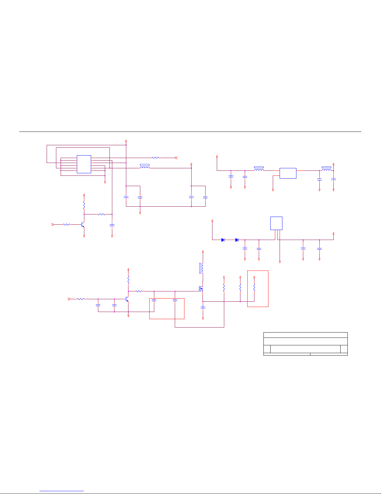
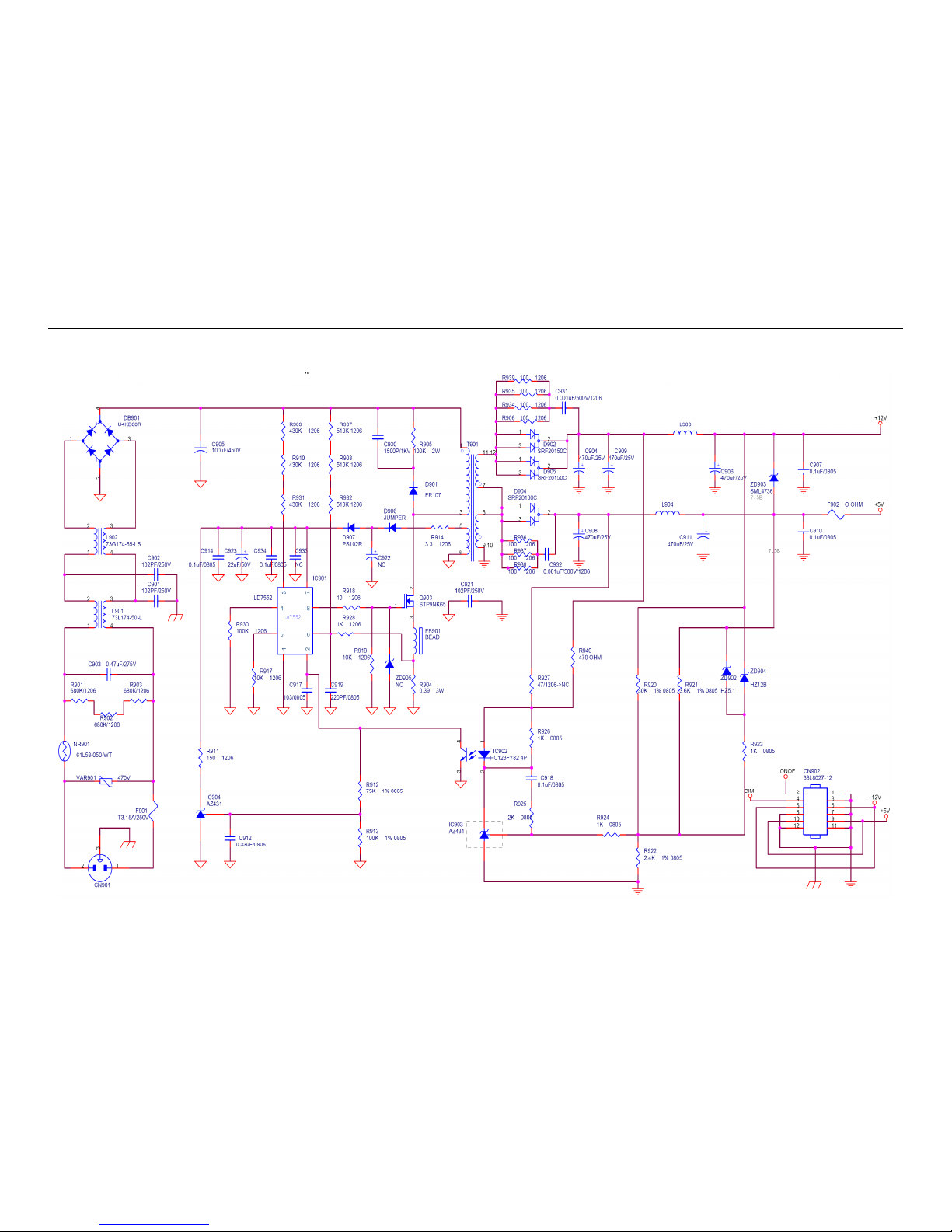
6.2 Power Board
715G1695-1
Page 24

19” LCD Color Monitor Gateway FPD1965
24
Page 25

19” LCD Color Monitor Gateway FPD1965
25
7. PCB Layout
7.1 Main Board
715G1691-1
Page 26

19” LCD Color Monitor Gateway FPD1965
26
7.2 Power Board
715G1695-1
7.3 Key Board
715G1707-1-2
715G1706-1
Page 27

19” LCD Color Monitor Gateway FPD1965
27
8. Maintainability
8.1 Equipments And Tools Requirement
1. Voltmeter.
2. Oscilloscope.
3. Pattern Generator.
4. DDC Tool with an IBM Compatible Computer.
5. Alignment Tool.
6. LCD Color Analyzer.
7. Service Manual.
8. User Manual.
Page 28

19” LCD Color Monitor Gateway FPD1965
28
8.2 Trouble Shooting
8.2.1 Main Board
No power
No power
Press power key and look
if the picture is normal
Please reinsert and make sure
the AC of 100-240 is normal
Measure U602 PIN2=1.8V
U601 PIN2=3.3V
Reinsert or check the
Adapter/Inverter
section
X301 oscillate waveforms
are normal
Check CN601 or replace
U601, U602
Replace U401
Replace X301
OK
OK
OK
NG
OK
NG
NG
Page 29

19” LCD Color Monitor Gateway FPD1965
29
No picture (LED orange)
No picture
Measure U602 PIN2=1.8V
U601 PIN2=3.3V
Replace U401
X301 oscillate
waveform is normal
Replace
U601, U602
OK
OK
OK
NG
Check HS/VS from
CN202 is normal
Replace X301
Check Correspondent
component
NG
NG
Replace U401
Whether the reset
of the Scalar IC is
useful?
Check U302, C333,
C329, ZD301
NG
OK
Page 30

19” LCD Color Monitor Gateway FPD1965
30
White screen
White screen
Measure Q603 base
is low level?
X301 oscillate
waveform is normal
Check Q603, Q602 is
broken or CN501 solder?
Check Correspondent
component.
Replace PANEL
Check Correspondent
component.
Replace U401
OK
OK
OK
Replace X301
OK
NG
NG
NG
NG
Check reset circuit of
U401 is normal
Page 31

19” LCD Color Monitor Gateway FPD1965
31
8.2.2 Power/Inverter Board
No power
Check bridge rectified circuit and F901 circut
1) Check IC901
2) Check IC904, D906, D907…OVP circuit
Check CN902 pin5, 6 = 12V
Check the voltage of C905(+)
Check start voltage for the pin3 of IC901
Check R909,R910,R931 and Change IC901
NG
Check the auxiliary voltage is bigger than
10V and smaller than 20V
NG
NG
NG
Check Q903, R904, T901, D902, D904,
D905, L903, L904, ZD902, ZD904
Check IC901 pin8 PWM wave
Check IC901
NG
OK
NG
OK
OK
OK
OK
Check AC line volt 110V or 220V
Check AC input
Page 32

19” LCD Color Monitor Gateway FPD1965
32
W / LED, No Backlight
Check VDDA, ENA
VDDA=4.75~5.25V
;
ENA>3V
OK
NG
Check On/Off loop Circuit
Check ISEN(pin5) normally
Check ISEN loop components
NG
End Striking function debug
Connect TIMER (Pin3) to GND
Check ENA(pin10), OVPT(pin7), CT(pin13), DRV1(pin1),
DRV2
(p
in15) of IC801
Check half bridge power conversion
circuit and Transformer output circuit
OK
NG
Change IC801
OK
OK
Check VSEN(pin6) of IC801
Judge VSEN>0.7V&<OVPT
OK
Check VSEN circuit form lamp’s
return to VSEN(pin6) of IC801
NG
Check pin3 voltage of D801,
D803<2V
OK
End VSEN circuit and
Protection loop debug
Check Protection
circuit, Components
short, open or fail
NG
OK
Page 33
19” LCD Color Monitor Gateway FPD1965
33
8.2.3 Keypad Board
OSD is unstable or not working
Is Key Pad Board connecting normally?
Connect Key Pad Board
Is Button Switch normally?
Replace Button Switch
Y
N
N
Is Key Pad Board normally?
Replace Key Pad Board
Y
N
Y
Check Main Board
Page 34

19” LCD Color Monitor Gateway FPD1965
34
9. White-Balance, Luminance Adjustment
Approximately 30 minutes should be allowed for warm up before proceeding White-Balance adjustment.
1. How to do the Chroma-7120 MEM. Channel setting
A. Reference to chroma 7120 user guide
B. Use “ SC” key and “ NEXT” key to modify x,yY value and use “ID” key to modify the
TEXT description Following is the procedure to do white-balance adjust
2. Setting the color temp. you want
A. MEM.CHANNEL 3 (7800 color):
7800 color temp. parameter is x = 283±30, y = 298 ±30, Y = 180 cd/m
2 ,
B. MEM.CHANNEL 4 (6500 color):
6500 color temp. parameter is x = 313±30, y = 329 ±30, Y =180 cd/m2
3. Into factory mode of Gateway FPD1965
Turn on power, press the MENU button, pull out the power cord, and then plug the power cord. Then the factory
OSD will be at the left top of the panel.
4. Bias adjustment:
Set the Contrast
to 50; Adjust the Brightness to 80.
5. Gain adjustment:
Move cursor to “-F-” and press MENU key
A. Adjust 7800 color-temperature
1. Switch the Chroma-7120 to RGB-Mode (with press “MODE” button)
2. Switch the MEM. Channel to Channel 3 (with up or down arrow on chroma 7120)
3. The LCD-indicator on chroma 7120 will show x = 283 ±30, y = 298 ±30, Y =180 cd/m
2
4. Adjust the RED of color1 on factory window until chroma 7120 indicator reached the value R=100
5. Adjust the GREEN of color1 on factory window until chroma 7120 indicator reached the value G=100
6. Adjust the BLUE of color1 on factory window until chroma 7120 indicator reached the value B=100
7. Repeat above procedure (item 4,5,6) until chroma 7120 RGB value meet the tolerance =100±2
B. Adjust 6500 color-temperature
1. Switch the chroma-7120 to RGB-Mode (with press “MODE” button)
2. Switch the MEM.channel to Channel 4(with up or down arrow on chroma 7120)
3. The LCD-indicator on chroma 7120 will show x = 313 ±30, y = 329 ±30, Y = 180 cd/m
2
4. Adjust the RED of color3 on factory window until chroma 7120 indicator reached the value R=100
5. Adjust the GREEN of color3 on factory window until chroma 7120 indicator reachedthe value G=100
6. Adjust the BLUE of color3 on factory window until chroma 7120 indicator reached the value B=100
7. Repeat above procedure (item 4,5,6) until chroma 7120 RGB value meet the tolerance =100±2
C. Turn the Power-button off to quit from factory mode.
Page 35

19” LCD Color Monitor Gateway FPD1965
35
10. Monitor Exploded View
NO. Part Name Part Number NO. Part Name Part Number
1 LEFT PLATE 23G3155-915-9A 13 BASE T34G6324 TL B
2 BEZEL 34G6325ATN B 14 BASE PLATE 15G6276-1
3 HOLD BRACKET-L 15G6295-1 15 RUBBER PAD 012G6215 1
4 PANEL 750GLK90E11 16 HINGE 37G6045-3
5 METAL COVER 15G6274-1 17 MECK BRACKET 15G6275-1
6 MYLAR 52G6025- 11-930 18 HOLD BRACKET-R 15G6296-1
7 MAIN BOARD CBPC980KKCGYNP 19 RIGHT PLATE 23G3155-915-10A
8 METAL CASE 15G6273-2 20 POWER BOARD PWPC1942CMW1P
9 REAR COVER 34G6326-TL-B 21 POWER BUTTON 033G6368 TN L
10 MYLAR 52G6025- 11-931 22 POWER LENS 33G6371-1-C
11 WIRE CLAMP 33G6366-TL-L 24 KEY BOARD KEPC780KGGP
12 STAND 34G6321-TL-B
Page 36

19” LCD Color Monitor Gateway FPD1965
36
11. BOM List
T980KKCHKGGKNP
Location Part NO. Description
007G 5 L122 Compound Pallet
011G6095 1 SHORE
011G6099 1 SUPPORT
012G6215 1 RUBBER PAD
015G6273 2 METAL CASE
015G6274 1 METAL COVER
015G6295 1 HOLD BKT-L
015G6296 1 HOLD BKT-R
023G3178915 2A Gateway LOGO
033G6367 TL L HINGE COVER
033G6368 TN L POWER BUTTON
033G6369 TL L BUTTON-FUNC
033G6371 1 C POWER LENS
034G6326 TL B REAR COVER
037G6045 3 HINGE
040G 17N915 3A RATING LABEL
040G 58162435A LABEL
040G 58162461A EPA LABEL
040G 581915 3A Gateway LOGO LABEL
040G 581915 4A DVI LABEL
040G 581915 5A AC LABEL
040G 581915 7A TECH SUPPORT
040G 582915 8A CARTON LABEL
041G780091513A WARRANTY CARD
041G780091515A SALE CARD
044G3942 1 EPS(L)
044G3942 2 EPS(R)
044G3942 3EPE EPE
044G3942915 2A CARTON
044G6002689 1A CARTON PLATE
044G9003 1 CORNER PAPER
045G 76 28 RN PE BAG FO MANUAL/BASE
045G 76 31 RN PR BAG FOR BASE
045G 88609GT2 EPE BAG
050G 600 2 HANDLE1
050G 600 3 HANDLE2
Page 37

19” LCD Color Monitor Gateway FPD1965
37
052G 1185 MIDDLE TAPE FOR CARTON
052G 1186 SMALL TAPE
052G 1209500 AL TAPE
052G6025 11930 MYLAR
052G6025 11931 MYLAR
E089B 089G1738LAA DG SIGNAL CABLE
089G602A18N IS POWER CORD
E095A 095G8014 10522 X WIRE HARNESS
E095B 095G8014 16667 X WIRE HARNESS
095G8018 30663 LVDS CABLE
095G8019 2502 INVERTER LINE
0M1G 130 4128 SCREW
0M1G 330 4128 SCREW M3X4
0M1G1340 5 47 SCREW
0M1G1730 6128 SCREW M3x6
0M1G1740 6128 SCREW
0M1G1740 8128 SCREW M4X8
0M1G1740 12225 SCREW
0M1G3130 5125 SCREW
0Q1G 330 5128 SCREW
0Q1G 330 6128 SCREW
0Q1G 330 8 47 SCREW 3X8mm
0Q1G 330 8128 SCREW PH K30X8 PT
705G980KP34027 19" LCD COVER ASS'Y
E750L 750GLK90E11 PANEL LCD 19" E01-100 5611 BOE-HYDIS
CBPC980KKCGYNP CONVERSION BOARD
KEPC780KGGP KEY BOARD
KEPC786HG1P KEY BOARD
PWPC1942CMW1P POWER BOARD
Q12G6300 28 RUBBER PAD
Q41G780091517A SETUP POSTER
Q41G780091519A Manual
015G6275 1 MECK BKT
015G6276 1 BASE PLATE
023G3155915 9A LEFT PLATE
023G315591510A RIGHT PLATE
033G6366 TL L WIRE CLAMP
034G6321 TL B STAND
034G6325ATN B BEZEL
Page 38

19” LCD Color Monitor Gateway FPD1965
38
0Q1G 330 6120 SCREW
0Q1G2430 6120 SCREW
T34G6324 TL B BASE
CN601 033G8027 12 WAFER 2*6P 2.0MM R/A
CN402 033G8027 12 WAFER 2*6P 2.0MM R/A
CN501 033G8027 24 CONN W TO B 12P*2 P*2.0 4504-2
040G 457624 1B LABEL-CPU
040G 45762412B CBPC LABEL
C601 067G215V221 4R LOW E.S.R 220UF +/-20% 25V
C611 067G215V221 4R LOW E.S.R 220UF +/-20% 25V
C606 067G215V221 4R LOW E.S.R 220UF +/-20% 25V
C602 067G215V221 4R LOW E.S.R 220UF +/-20% 25V
C615 067G215Y2207RV RUBYCON 50V 22UF
C610 067G215Y2207RV RUBYCON 50V 22UF
C501 067G215Y2207RV RUBYCON 50V 22UF
C325 067G215Y2207RV RUBYCON 50V 22UF
C319 067G215Y2207RV RUBYCON 50V 22UF
C316 067G215Y2207RV RUBYCON 50V 22UF
C309 067G215Y2207RV RUBYCON 50V 22UF
C301 067G215Y2207RV RUBYCON 50V 22UF
CN202 088G 35315F H D-SUB 15PIN
CN201 088G 35424F H DV1 CONNECTOR 24PIN
U401 090G6250 1 GP HEAT SINK
X301 093G 22 53 CRYSTAL 14.318MHzHC-49US
CN101 033G3802 4H WAFER 4P RIGHT ANGLE
SW101 077G 605 1 CJ TSAB-2
DP101 081G 12 7 GP LED
715G1707 1 2 KEY BOARD PCB
CN802 033G8021 2D U 3.5mm WAFER
CN801 033G8021 2D U 3.5mm WAFER
CN803 033G8021 2D U 3.5mm WAFER
CN804 033G8021 2D U 3.5mm WAFER
040G 45762420A GP CBPC LABEL 25X6mm
IC902 056G 139 3B PC123 Y82FZ0F
R904 061G 2J478 59 0.47 2W
VAR901 061G 46 6 GP TNR 10V471K
R905 061G152M10458F 100K OHM 5% 2W
C816 065G 3J1206ET 12PF 5% SL 3KV TDK
C825 065G 3J1206ET 12PF 5% SL 3KV TDK
Page 39

19” LCD Color Monitor Gateway FPD1965
39
C817 065G 3J5096ET 5PF 5% SL 3KV
C826 065G 3J5096ET 5PF 5% SL 3KV
C901 065G306M1022BP 1000PF Y1.CAP
C902 065G306M1022BP 1000PF Y1.CAP
C921 065G306M1022BP 1000PF Y1.CAP
C820 067G215D471 4K ED 470UF 25V
C811 067G215D471 4K ED 470UF 25V
C911 067G215D471 4K ED 470UF 25V
C909 067G215D471 4K ED 470UF 25V
C908 067G215D471 4K ED 470UF 25V
C906 067G215D471 4K ED 470UF 25V
C904 067G215D471 4K ED 470UF 25V
C905 067G215S10115K 100UF 450V
L903 073G 253 91 L CHOKE BY LI TA
L904 073G 253 91 L CHOKE BY LI TA
L901 073L 174 50 LH LINE FILTER
T901 080GL19T 13 N TRANSFORMER
HS3 090G6276 1 V HEATSINK
DB901 093G 50460900 BRIDEGE DIODE GBU408 LITEON
D907 093G 6038T52T FR103
CN902 095G8014 12531 WIRE HARNESS
705G 560 61GTW NR901 ASS'Y
705G 780 57 05 Q903 ASS'Y
705G 780 87 20 AC SOCKET ASS'Y
705G 780 93 05 D902 ASS'Y
U401 056G 562 97 GM 5621-LF-AA
U601 056G 563 7 AIC1084-33PM
U602 056G 563 31 AI1117D-1.8-EI
U302 056G 643 13 G691L400T73UF SOT-23 GMT
U202 056G1133 34 M24C02-WMN6TP
U201 056G1133 34 M24C02-WMN6TP
U402 056G1133 59KG1 SST25VF010
Q601 057G 417 4 PMBS3904/PHILIPS-SMT(04)
Q603 057G 417 4 PMBS3904/PHILIPS-SMT(04)
Q401 057G 417 6 PMBS3906/PHILIPS-SMT(06)
Q403 057G 417 6 PMBS3906/PHILIPS-SMT(06)
Q404 057G 417 6 PMBS3906/PHILIPS-SMT(06)
Q201 057G 758 1 2N7002ESOT23 SILICONIX
Q602 057G 763 1 A03401 SOT23 BY AOS(A1)
Page 40

19” LCD Color Monitor Gateway FPD1965
40
R606 061L0603000 RST SM 0603 JUMP MAX 0R05 R
R243 061L0603000 RST SM 0603 JUMP MAX 0R05 R
R429 061L0603000 RST SM 0603 JUMP MAX 0R05 R
R331 061L0603000 RST SM 0603 JUMP MAX 0R05 R
R301 061L0603100 CHIP 10 OHM 1/10W
R209 061L0603100 CHIP 10 OHM 1/10W
R208 061L0603100 CHIP 10 OHM 1/10W
R207 061L0603100 CHIP 10 OHM 1/10W
R206 061L0603100 CHIP 10 OHM 1/10W
R205 061L0603100 CHIP 10 OHM 1/10W
R204 061L0603100 CHIP 10 OHM 1/10W
R203 061L0603100 CHIP 10 OHM 1/10W
R202 061L0603100 CHIP 10 OHM 1/10W
R417 061L0603100 2F 10K 1% 1/10W
R416 061L0603100 2F 10K 1% 1/10W
R214 061L0603100 2F 10K 1% 1/10W
R408 061L0603101 CHIPR 100 OHM +-5% 1/16W
R407 061L0603101 CHIPR 100 OHM +-5% 1/16W
R230 061L0603101 CHIPR 100 OHM +-5% 1/16W
R224 061L0603101 CHIPR 100 OHM +-5% 1/16W
R222 061L0603101 CHIPR 100 OHM +-5% 1/16W
R329 061L0603102 CHIPR 1K OHM +-5% 1/16W
R501 061L0603102 CHIPR 1K OHM +-5% 1/16W
R602 061L0603102 CHIPR 1K OHM +-5% 1/16W
R603 061L0603102 CHIPR 1K OHM +-5% 1/16W
R609 061L0603103 CHIPR 10K OHM +-5% 1/16W
R608 061L0603103 CHIPR 10K OHM +-5% 1/16W
R431 061L0603103 CHIPR 10K OHM +-5% 1/16W
R330 061L0603103 CHIPR 10K OHM +-5% 1/16W
R418 061L0603103 CHIPR 10K OHM +-5% 1/16W
R430 061L0603103 CHIPR 10K OHM +-5% 1/16W
R242 061L0603103 CHIPR 10K OHM +-5% 1/16W
R211 061L0603103 CHIPR 10K OHM +-5% 1/16W
R201 061L0603103 CHIPR 10K OHM +-5% 1/16W
R605 061L0603104 RST SM 0603 RC0603 100K PM5 R
R232 061L0603221 CHIPR 220 OHM+-5% 1/16W
R237 061L0603221 CHIPR 220 OHM+-5% 1/16W
R238 061L0603221 CHIPR 220 OHM+-5% 1/16W
R239 061L0603221 CHIPR 220 OHM+-5% 1/16W
Page 41

19” LCD Color Monitor Gateway FPD1965
41
R411 061L0603221 CHIPR 220 OHM+-5% 1/16W
R412 061L0603221 CHIPR 220 OHM+-5% 1/16W
R413 061L0603221 CHIPR 220 OHM+-5% 1/16W
R414 061L0603221 CHIPR 220 OHM+-5% 1/16W
R415 061L0603221 CHIPR 220 OHM+-5% 1/16W
R432 061L0603221 CHIPR 220 OHM+-5% 1/16W
R228 061L0603221 CHIPR 220 OHM+-5% 1/16W
R216 061L0603221 CHIPR 220 OHM+-5% 1/16W
R215 061L0603221 CHIPR 220 OHM+-5% 1/16W
R210 061L0603221 CHIPR 220 OHM+-5% 1/16W
R241 061L0603222 CHIPR 2.2K OHM+-5% 1/16W
R240 061L0603222 CHIPR 2.2K OHM+-5% 1/16W
R217 061L0603223 CHIPR 22K OHM +-5% 1/16W
R409 061L0603223 CHIPR 22K OHM +-5% 1/16W
R410 061L0603223 CHIPR 22K OHM +-5% 1/16W
R420 061L0603223 CHIPR 22K OHM +-5% 1/16W
R421 061L0603223 CHIPR 22K OHM +-5% 1/16W
R302 061L0603249 0F CHIP 249OHM 1/16W 1%
R422 061L0603303 CHIP 30K OHM 5% 1/16W
R419 061L0603303 CHIP 30K OHM 5% 1/16W
R218 061L0603303 CHIP 30K OHM 5% 1/16W
R227 061L0603472 CHIPR 4.7K OHM +-5% 1/16W
R305 061L0603472 CHIPR 4.7K OHM +-5% 1/16W
R315 061L0603472 CHIPR 4.7K OHM +-5% 1/16W
R601 061L0603472 CHIPR 4.7K OHM +-5% 1/16W
R316 061L0603472 CHIPR 4.7K OHM +-5% 1/16W
R317 061L0603472 CHIPR 4.7K OHM +-5% 1/16W
R323 061L0603472 CHIPR 4.7K OHM +-5% 1/16W
R324 061L0603472 CHIPR 4.7K OHM +-5% 1/16W
R424 061L0603472 CHIPR 4.7K OHM +-5% 1/16W
R226 061L0603472 CHIPR 4.7K OHM +-5% 1/16W
R213 061L0603472 CHIPR 4.7K OHM +-5% 1/16W
R212 061L0603472 CHIPR 4.7K OHM +-5% 1/16W
R604 061L0603473 RST SM 0603 RC0603 47K PM5 R
R428 061L0603473 RST SM 0603 RC0603 47K PM5 R
R405 061L0603473 RST SM 0603 RC0603 47K PM5 R
R229 061L0603750 CHIPR 75 OHM+-5% 1/16W
R223 061L0603750 CHIPR 75 OHM+-5% 1/16W
R220 061L0603750 CHIPR 75 OHM+-5% 1/16W
Page 42

19” LCD Color Monitor Gateway FPD1965
42
R235 061L0603750 9F 75OHM 1% 1/10W
R234 061L0603750 9F 75OHM 1% 1/10W
R233 061L0603750 9F 75OHM 1% 1/10W
FB605 061L0805000 CHIPR 0OHM +-5% 1/10W
C421 065G0603102 32 1000PF +-10% 50V X7R
C420 065G0603102 32 1000PF +-10% 50V X7R
C416 065G0603102 32 1000PF +-10% 50V X7R
C413 065G0603102 32 1000PF +-10% 50V X7R
C414 065G0603102 32 1000PF +-10% 50V X7R
C415 065G0603102 32 1000PF +-10% 50V X7R
C412 065G0603102 32 1000PF +-10% 50V X7R
C411 065G0603102 32 1000PF +-10% 50V X7R
C407 065G0603102 32 1000PF +-10% 50V X7R
C406 065G0603102 32 1000PF +-10% 50V X7R
C405 065G0603102 32 1000PF +-10% 50V X7R
C404 065G0603102 32 1000PF +-10% 50V X7R
C201 065G0603102 32 1000PF +-10% 50V X7R
C329 065G0603103 32 0.01UF +-10% 50V X7R
C330 065G0603104 12 CER2 0603 X7R 16V 100N PM10 R
C326 065G0603104 12 CER2 0603 X7R 16V 100N PM10 R
C324 065G0603104 12 CER2 0603 X7R 16V 100N PM10 R
C323 065G0603104 12 CER2 0603 X7R 16V 100N PM10 R
C322 065G0603104 12 CER2 0603 X7R 16V 100N PM10 R
C321 065G0603104 12 CER2 0603 X7R 16V 100N PM10 R
C320 065G0603104 12 CER2 0603 X7R 16V 100N PM10 R
C318 065G0603104 12 CER2 0603 X7R 16V 100N PM10 R
C317 065G0603104 12 CER2 0603 X7R 16V 100N PM10 R
C314 065G0603104 12 CER2 0603 X7R 16V 100N PM10 R
C333 065G0603104 12 CER2 0603 X7R 16V 100N PM10 R
C334 065G0603104 12 CER2 0603 X7R 16V 100N PM10 R
C335 065G0603104 12 CER2 0603 X7R 16V 100N PM10 R
C408 065G0603104 12 CER2 0603 X7R 16V 100N PM10 R
C502 065G0603104 12 CER2 0603 X7R 16V 100N PM10 R
C603 065G0603104 12 CER2 0603 X7R 16V 100N PM10 R
C604 065G0603104 12 CER2 0603 X7R 16V 100N PM10 R
C608 065G0603104 12 CER2 0603 X7R 16V 100N PM10 R
C612 065G0603104 12 CER2 0603 X7R 16V 100N PM10 R
C613 065G0603104 12 CER2 0603 X7R 16V 100N PM10 R
C614 065G0603104 12 CER2 0603 X7R 16V 100N PM10 R
Page 43

19” LCD Color Monitor Gateway FPD1965
43
C209 065G0603104 12 CER2 0603 X7R 16V 100N PM10 R
C214 065G0603104 12 CER2 0603 X7R 16V 100N PM10 R
C219 065G0603104 12 CER2 0603 X7R 16V 100N PM10 R
C220 065G0603104 12 CER2 0603 X7R 16V 100N PM10 R
C302 065G0603104 12 CER2 0603 X7R 16V 100N PM10 R
C303 065G0603104 12 CER2 0603 X7R 16V 100N PM10 R
C304 065G0603104 12 CER2 0603 X7R 16V 100N PM10 R
C305 065G0603104 12 CER2 0603 X7R 16V 100N PM10 R
C313 065G0603104 12 CER2 0603 X7R 16V 100N PM10 R
C312 065G0603104 12 CER2 0603 X7R 16V 100N PM10 R
C311 065G0603104 12 CER2 0603 X7R 16V 100N PM10 R
C310 065G0603104 12 CER2 0603 X7R 16V 100N PM10 R
C308 065G0603104 12 CER2 0603 X7R 16V 100N PM10 R
C307 065G0603104 12 CER2 0603 X7R 16V 100N PM10 R
C306 065G0603104 12 CER2 0603 X7R 16V 100N PM10 R
C618 065G0603104 32 CHIP 0.1UF 50V X7R
C616 065G0603105 12 CHIP 1UF 16VX7R 0603
C332 065G0603224 12 CHIP 0.22UF +-10% 16V X7R
C328 065G0603330 31 CER1 0603 NP0 50V 33P PM5 R
C327 065G0603330 31 CER1 0603 NP0 50V 33P PM5 R
C210 065G0603473 32 CHIP 0.047UF 50V X7R
C211 065G0603473 32 CHIP 0.047UF 50V X7R
C212 065G0603473 32 CHIP 0.047UF 50V X7R
C216 065G0603473 32 CHIP 0.047UF 50V X7R
C215 065G0603473 32 CHIP 0.047UF 50V X7R
C213 065G0603473 32 CHIP 0.047UF 50V X7R
L306 071G 56K121 CHIP BEAD
L305 071G 56K121 CHIP BEAD
L304 071G 56K121 CHIP BEAD
L303 071G 56K121 CHIP BEAD
L302 071G 56K121 CHIP BEAD
L301 071G 56K121 CHIP BEAD
FB204 071G 59B431 BK1608 HW 431
L405 071G 59C600 CHIP BEAD
L404 071G 59C600 CHIP BEAD
L403 071G 59C600 CHIP BEAD
L402 071G 59C600 CHIP BEAD
L401 071G 59C600 CHIP BEAD
FB203 071G 59C600 CHIP BEAD
Page 44

19” LCD Color Monitor Gateway FPD1965
44
FB202 071G 59C600 CHIP BEAD
FB201 071G 59C600 CHIP BEAD
D211 093G 64 33 DIO SIG SM BAV99 (PHSE)R
D212 093G 64 33 DIO SIG SM BAV99 (PHSE)R
D213 093G 64 33 DIO SIG SM BAV99 (PHSE)R
ED108 093G 64 40 PC SGX1608
ED107 093G 64 40 PC SGX1608
ED106 093G 64 40 PC SGX1608
ED105 093G 64 40 PC SGX1608
ED104 093G 64 40 PC SGX1608
ED103 093G 64 40 PC SGX1608
ED102 093G 64 40 PC SGX1608
ED101 093G 64 40 PC SGX1608
D210 093G 64 42 P BAV70 SOT-23
D209 093G 64 42 P BAV70 SOT-23
ZD301 093G 64 49 SU EGA10603 V05
ZD215 093G 64 49 SU EGA10603 V05
ZD214 093G 64 49 SU EGA10603 V05
ZD213 093G 64 49 SU EGA10603 V05
ZD212 093G 64 49 SU EGA10603 V05
ZD406 093G 39S 34 T UDZS5.6B
ZD405 093G 39S 34 T UDZS5.6B
ZD401 093G 39S 34 T UDZS5.6B
ZD402 093G 39S 34 T UDZS5.6B
ZD403 093G 39S 34 T UDZS5.6B
ZD404 093G 39S 34 T UDZS5.6B
ZD211 093G 39S 34 T UDZS5.6B
ZD210 093G 39S 34 T UDZS5.6B
ZD209 093G 39S 34 T UDZS5.6B
ZD208 093G 39S 34 T UDZS5.6B
ZD207 093G 39S 34 T UDZS5.6B
ZD204 093G 39S 34 T UDZS5.6B
ZD203 093G 39S 34 T UDZS5.6B
ZD202 093G 39S 34 T UDZS5.6B
ZD201 093G 39S 34 T UDZS5.6B
D602 093G2040 3F FA20-04
D601 093G2040 3F FA20-04
715G1691 1 PCB BOARD
CN102 033G8034 6S 6PIN 1MM
Page 45

19” LCD Color Monitor Gateway FPD1965
45
SW102 077G 606501 CJ TACT SWITCH
SW103 077G 606501 CJ TACT SWITCH
SW104 077G 606501 CJ TACT SWITCH
SW105 077G 606501 CJ TACT SWITCH
SW106 077G 606501 CJ TACT SWITCH
715G1706 1 PCB BOARD
NR901 061G 58050 WT NTC 5 OHM 5A
096G 29 10 H.S.TUBE
Q903 057G 724 11 STP9NK65ZFP
090G6274 1 L HEATSINK
0M1T1730 8128 SCREW M3x8
CN901 087G 504501 S AC SOCKET ST-03
CN901 095G 900567 WIRE HARNESS
CN901 096G 29 6 SHRINK TUBE UL/CSA
090G6275 1 N HEAT SINK
D905 093G 60242 SRF20150C T0-220
D902 093G 60242 SRF20150C T0-220
D904 093G 60248 SP20100
0M1T1730 8128 SCREW M3x8
IC901 056G 379 52 LD7552BS
IC801 056G 608 10 0Z9938
Q803 057G 417 4 PMBS3904/PHILIPS-SMT(04)
Q802 057G 417 4 PMBS3904/PHILIPS-SMT(04)
Q801 057G 417 4 PMBS3904/PHILIPS-SMT(04)
Q806 057G 763 14 AM9945N
Q805 057G 763 14 AM9945N
R840 061L0805000 CHIPR 0OHM +-5% 1/10W
R842 061L0805000 CHIPR 0OHM +-5% 1/10W
R913 061L0805100 3F CHIP 100KOHM +-1% 1/8W
R841 061L0805102 CHIPR 1K OHM +-5% 1/10W
R843 061L0805102 CHIPR 1K OHM +-5% 1/10W
R923 061L0805102 CHIPR 1K OHM +-5% 1/10W
R924 061L0805102 CHIPR 1K OHM +-5% 1/10W
R926 061L0805102 CHIPR 1K OHM +-5% 1/10W
R812 061L0805103 CHIPR 10K OHM +-5% 1/10W
R830 061L0805153 CHIPR 15K OHM+-5% 1/8W
R820 061L0805153 CHIPR 15K OHM+-5% 1/8W
R925 061L0805202 CHIP 2KOHM 1/8W
R922 061L0805240 1F CHIPR 2.4KOHM +-1% 1/8W
Page 46

19” LCD Color Monitor Gateway FPD1965
46
C808 061L0805274 270K OHM 1/8W
R920 061L0805303 CHIP 30K OHM 1/8W
R921 061L0805360 1F CHIP 3.6KOHM 1/8W 1%
R834 061L0805392 CHIP 3.9K OHM 1/8W
R827 061L0805392 CHIP 3.9K OHM 1/8W
R835 061L0805561 CHIP 560 OHM 1/8W
R825 061L0805561 CHIP 560 OHM 1/8W
R912 061L0805750 2F cHIP 75KOHM 1% 1/8W
R831 061L0805913 CHIPR 91K 0HM+-5% 1/8W
R821 061L0805913 CHIPR 91K 0HM+-5% 1/8W
F902 061L1206000 CHIPR 0 OHM +-5% 1/8W
R801 061L1206000 CHIPR 0 OHM +-5% 1/8W
JR802 061L1206000 CHIPR 0 OHM +-5% 1/8W
JR801 061L1206000 CHIPR 0 OHM +-5% 1/8W
J805 061L1206000 CHIPR 0 OHM +-5% 1/8W
R918 061L1206100 CHIPR 10 OHM+-5% 1/8W
R837 061L1206100 CHIPR 10 OHM+-5% 1/8W
R836 061L1206100 CHIPR 10 OHM+-5% 1/8W
R930 061L1206100 3F CHIP 100K OHM +-1% 1/4W
R906 061L1206101 CHIP 100 OHM 5% 1/8W
R934 061L1206101 CHIP 100 OHM 5% 1/8W
R935 061L1206101 CHIP 100 OHM 5% 1/8W
R936 061L1206101 CHIP 100 OHM 5% 1/8W
R939 061L1206101 CHIP 100 OHM 5% 1/8W
R938 061L1206101 CHIP 100 OHM 5% 1/8W
R937 061L1206101 CHIP 100 OHM 5% 1/8W
R928 061L1206102 CHIP 1K OHM 5% 1/8W
R917 061L1206103 CHIP 10KOHM 5% 1/4W
R919 061L1206103 CHIP 10KOHM 5% 1/4W
R804 061L1206103 CHIP 10KOHM 5% 1/4W
R803 061L1206103 CHIP 10KOHM 5% 1/4W
R808 061L1206104 CHIP 100KOHM 5% 1/4W
R815 061L1206104 CHIP 100KOHM 5% 1/4W
R813 061L1206105 CHIP 1MOHM 5% 1/4W
R810 061L1206105 CHIP 1MOHM 5% 1/4W
R911 061L1206151 CHIP 150OHM 1/4W
R816 061L1206155 1.5M/0805
R826 061L1206182 0F CHIP 180 OHM 1/4W
R829 061L1206220 CHIP 22OHM 5% 8W
Page 47

19” LCD Color Monitor Gateway FPD1965
47
R828 061L1206220 CHIP 22OHM 5% 8W
R819 061L1206220 CHIP 22OHM 5% 8W
R818 061L1206220 CHIP 22OHM 5% 8W
R807 061L1206220 CHIP 22OHM 5% 8W
R802 061L1206274 CHIP 270K OHM 1/4W
R914 061L1206339 CHIP 3.3OHM 1/4W
R931 061L1206434 430K 1206 1/4W 5%
R910 061L1206434 430K 1206 1/4W 5%
R909 061L1206434 430K 1206 1/4W 5%
R817 061L1206464 2F RST CHIPR 46.4KOHM +-1% 1/4W
R805 061L1206471 CHIPR 470 OHM+-5% 1/8W
R908 061L1206514 CHIPR 510KOHM +-5% 1/4W
R907 061L1206514 CHIPR 510KOHM +-5% 1/4W
R932 061L1206514 CHIPR 510KOHM +-5% 1/4W
R814 061L1206684 CHIPR 680K OHM+-5% 1/8W
R901 061L1206684 CHIPR 680K OHM+-5% 1/8W
R902 061L1206684 CHIPR 680K OHM+-5% 1/8W
R903 061L1206684 CHIPR 680K OHM+-5% 1/8W
C805 065G0805102 31 1000PF 50V NPO
C807 065G0805103 22 CHIP 0.01uF 25V X7R 0805
C910 065G0805104 22 0.1UF +-10% 25V X7R 080
C907 065G0805104 22 0.1UF +-10% 25V X7R 080
C914 065G0805104 22 0.1UF +-10% 25V X7R 080
C918 065G0805104 22 0.1UF +-10% 25V X7R 080
C934 065G0805104 22 0.1UF +-10% 25V X7R 080
C933 065G0805104 32 CHIP 0.1U 50V X7R
C804 065G0805155 A2 1.5 UF 10V
C919 065G0805221 21 220PF 25V 5%
C917 065G0805223 22 CHIP 0.022UF 25V X7R 0805
C809 065G0805223 22 CHIP 0.022UF 25V X7R 0805
C912 065G0805334 22 0.33UF+-10% 25V X7R 0805
C827 065G0805471 21 CHIP 470PF 25V NPO
C818 065G0805471 21 CHIP 470PF 25V NPO
C810 065G080547121G 470PF, G, 25V,NPO
C819 065G0805683 22 68NK X7R 25V
C813 065G1206222 32 2.2N/50V
C823 065G1206222 32 2.2N/50V
C822 065G1206222 32 2.2N/50V
C812 065G1206222 32 2.2N/50V
Page 48

19” LCD Color Monitor Gateway FPD1965
48
C806 065G1206225 22 2.2UF 25V X7R 1206
D803 093G 64 42 P BAV70 SOT-23
D801 093G 64 42 P BAV70 SOT-23
D804 093G 6433P BAV99
D802 093G 6433P BAV99
ZD902 093G 39S 17 T RLZ12B LLDS
ZD903 093G 39S 19 T PTZ7.5B
ZD801 093G 39S 24 T RLZ 5.6B LLDS
ZD904 093G 39S 25 T RLZ5.1B LLDS
034FPF20P01 BOBBIN
034FPE19P03 CASE EEL19
034FPE19P03 CASE EEL19
CN901 006G 31500 EYELET
T901 006G 31502 1.5MM RIVET
PT802 006G 31502 1.5MM RIVET
PT801 006G 31502 1.5MM RIVET
NR901 006G 31502 1.5MM RIVET
C905 006G 31502 1.5MM RIVET
715G1695 1 PCB
FB901 071G 55 29 FERRITE BEAD
L902 006G 31502 1.5MM RIVET
L901 006G 31502 1.5MM RIVET
IC904 056G 158 4 T H431BA
IC903 056G 158 4 T H431BA
R940 061G 60247152T 470OHM +-5% 1/6W
R822 061G212Y305 KT MGFR 3M OHM +-5% 1/2W
R832 061G212Y305 KT MGFR 3M OHM +-5% 1/2W
C930 065G 2K152 1T6921 1.5NF/2KV Y5P +-10%
C824 065G 444102 5T 1000PF 10% 50V CERAMIC
C821 065G 444102 5T 1000PF 10% 50V CERAMIC
C815 065G 444102 5T 1000PF 10% 50V CERAMIC
C814 065G 444102 5T 1000PF 10% 50V CERAMIC
C932 065G517K102 5T 1000PF 10% Y5P 500V
C931 065G517K102 5T 1000PF 10% Y5P 500V
C923 067G 2152207NT GP LOW ESR 22UF+-20% 50V BY CHEMI
F901 084G 56 1 FUSE 2A 250V WICKMANN
D901 093G 6026T52T RECTIFIER DIODE FR107
T95KGCHKDPGKNC
Page 49

19” LCD Color Monitor Gateway FPD1965
49
Location Part NO. Description
011G6095 1 SHORE
011G6099 1 SUPPORT
012G6215 1 RUBBER PAD
015G6273 2 METAL CASE
015G6274 1 METAL COVER
015G6295 1 HOLD BKT-L
015G6296 1 HOLD BKT-R
033G6368 TN L 30 KEY PAD
033G6369 TL L BUTTON-FUNC
033G6371 1 C POWER LENS
034G6326 TL B REAR COVER
037G6045 3 HINGE
040G 17N915 3A RATING LABEL
040G 58162461A EPA LABEL
040G 581915 3A Gateway LOGO LABEL
040G 581915 4A DVI LABEL
040G 581915 5A AC LABEL
040G 581915 7A TECH SUPPORT
040G 582915 8A CARTON LABEL
044G3942 1 EPS(L)
044G3942 2 EPS(R)
044G3942 3EPE EPE
044G3942915 2A CARTON
045G 88609GT2 EPE BAG
050G 600 2 HANDLE1
050G 600 3 HANDLE2
052G 1185 MIDDLE TAPE
052G 1186 SMALL TAPE
052G 1209500 AL TAPE
052G6025 11930 MYLAR
052G6025 11931 MYLAR
E089B 089G1738GAA DG SIGNAL CABLE
E089B 089G1738LAA DG SIGNAL CABLE
089G602A18N IS POWER CORD
E095A 095G8014 10522 D WIRE HARNESS
E095A 095G8014 10522 X WIRE HARNESS
E095B 095G8014 16667 D WIRE HARNESS
E095B 095G8014 16667 X WIRE HARNESS
095G8018 30663 LVDS CABLE
Page 50

19” LCD Color Monitor Gateway FPD1965
50
095G8019 2502 INVERTER LINE
0M1G 130 4128 CR3 SCREW
0M1G 330 4128 CR3 SCREW
0M1G1340 5 47 CR3 SCREW
0M1G1730 6128 CR3 SCREW
0M1G1740 6128 CR3 SCREW
0M1G1740 8128 CR3 SCREW
0M1G1740 12225 CR3 SCREW
0M1G3130 5125 SCREW
0Q1G 330 5128 CR3 SCREW
0Q1G 330 6128 CR3 SCREW
0Q1G 330 8 47 CR3 SCREW
0Q1G 330 8128 CR3 SCREW
705G980KP34027 19" LCD COVER ASS'Y
012G6113 1 BASE-FOOT
015G6275 1 MECK BKT
015G6276 1 BASE PLATE
023G3155915 9A LEFT PLATE
023G315591510A RIGHT PLATE
033G6366 TL L WIRE CLAMP
034G6321 TL B STAND
034G6325ATN B BEZEL
0Q1G 330 6120 SCREW
0Q1G2430 6120 SCREW
T34G6324 TL B BASE
E750L 750GLK90E1100N000W PANEL HT190E01-100 5611 GATEWAY BOE
CBPC980KKCGYNP MAIN BOARD
CN601 033G8027 12 WAFER 2*6P 2.0MM R/A
CN402 033G8027 12 WAFER 2*6P 2.0MM R/A
CN501 033G8027 24 CONN W TO B 12P*2 P*2.0 4504-2
040G 457624 1B LABEL-CPU
040G 45762412B CBPC LABEL
C601 067G215V221 4N KY25VB220-M-CC3 8*11.5MM
C602 067G215V221 4N KY25VB220-M-CC3 8*11.5MM
C606 067G215V221 4N KY25VB220-M-CC3 8*11.5MM
C611 067G215V221 4N KY25VB220-M-CC3 8*11.5MM
C601 067G215V221 4R LOW E.S.R 220UF +/-20% 2
C602 067G215V221 4R LOW E.S.R 220UF +/-20% 2
C606 067G215V221 4R LOW E.S.R 220UF +/-20% 2
C611 067G215V221 4R LOW E.S.R 220UF +/-20% 2
Page 51

19” LCD Color Monitor Gateway FPD1965
51
C301 067G215Y2207NV KY50VB22M-CC3 5*11
C309 067G215Y2207NV KY50VB22M-CC3 5*11
C316 067G215Y2207NV KY50VB22M-CC3 5*11
C319 067G215Y2207NV KY50VB22M-CC3 5*11
C325 067G215Y2207NV KY50VB22M-CC3 5*11
C501 067G215Y2207NV KY50VB22M-CC3 5*11
C610 067G215Y2207NV KY50VB22M-CC3 5*11
C615 067G215Y2207NV KY50VB22M-CC3 5*11
C301 067G215Y2207RV RUBYCON 50V 22UF
C309 067G215Y2207RV RUBYCON 50V 22UF
C316 067G215Y2207RV RUBYCON 50V 22UF
C319 067G215Y2207RV RUBYCON 50V 22UF
C325 067G215Y2207RV RUBYCON 50V 22UF
C501 067G215Y2207RV RUBYCON 50V 22UF
C610 067G215Y2207RV RUBYCON 50V 22UF
C615 067G215Y2207RV RUBYCON 50V 22UF
CN202 088G 35315F H D-SUB 15PIN
CN202 088G 35315F HJ SOC SUBD H 15P F
CN201 088G 35424F H DV1 CONNECTOR 24PIN
U401 090G6250 1 GP HEAT SINK
X301 093G 22 53 CRYSTAL 14.318MHzHC-49US
U401 056G 562 97 GM 5621-LF-AA
U601 056G 563 7 IC AIC1084-33PMTR-R AIC
U601 056G 563 21 AP1084K33LA
U602 056G 563 31 AI1117D-1.8-EI
U302 056G 643 13 G691L400T73UF SOT-23 GMT
U202 056G1133 34 M24C02-WMN6TP
U201 056G1133 34 M24C02-WMN6TP
U402 056G1133 59KG1 SST25VF010
U202 056G113334A 24LC02B/SNG SOIC-8PIN
U201 056G113334A 24LC02B/SNG SOIC-8PIN
Q603 057G 417 4 PMBS3904/PHILIPS-SMT(04)
Q601 057G 417 4 PMBS3904/PHILIPS-SMT(04)
Q404 057G 417 6 PMBS3906/PHILIPS-SMT(06)
Q403 057G 417 6 PMBS3906/PHILIPS-SMT(06)
Q401 057G 417 6 PMBS3906/PHILIPS-SMT(06)
Q201 057G 758 1 2N7002ESOT23 SILICONIX
Q602 057G 763 1 A03401 SOT23 BY AOS(A1)
R243 061G0603000 RST CHIPR 0 OHM +-5% 1/10W
R331 061G0603000 RST CHIPR 0 OHM +-5% 1/10W
Page 52

19” LCD Color Monitor Gateway FPD1965
52
R429 061G0603000 RST CHIPR 0 OHM +-5% 1/10W
R606 061G0603000 RST CHIPR 0 OHM +-5% 1/10W
R202 061G0603100 RST CHIPR 10 OHM +-5% 1/10W
R203 061G0603100 RST CHIPR 10 OHM +-5% 1/10W
R204 061G0603100 RST CHIPR 10 OHM +-5% 1/10W
R205 061G0603100 RST CHIPR 10 OHM +-5% 1/10W
R206 061G0603100 RST CHIPR 10 OHM +-5% 1/10W
R207 061G0603100 RST CHIPR 10 OHM +-5% 1/10W
R208 061G0603100 RST CHIPR 10 OHM +-5% 1/10W
R301 061G0603100 RST CHIPR 10 OHM +-5% 1/10W
R209 061G0603100 RST CHIPR 10 OHM +-5% 1/10W
R214 061G0603100 2F RST CHIPR 10 KOHM +-1% 1/10W
R416 061G0603100 2F RST CHIPR 10 KOHM +-1% 1/10W
R417 061G0603100 2F RST CHIPR 10 KOHM +-1% 1/10W
R222 061G0603101 RST CHIPR 100 OHM +-5% 1/10W
R224 061G0603101 RST CHIPR 100 OHM +-5% 1/10W
R230 061G0603101 RST CHIPR 100 OHM +-5% 1/10W
R408 061G0603101 RST CHIPR 100 OHM +-5% 1/10W
R407 061G0603101 RST CHIPR 100 OHM +-5% 1/10W
R603 061G0603102 RST CHIP 1K 1/10W 5%
R602 061G0603102 RST CHIP 1K 1/10W 5%
R501 061G0603102 RST CHIP 1K 1/10W 5%
R329 061G0603102 RST CHIP 1K 1/10W 5%
R201 061G0603103 RST CHIPR 10 KOHM +-5% 1/10W
R211 061G0603103 RST CHIPR 10 KOHM +-5% 1/10W
R242 061G0603103 RST CHIPR 10 KOHM +-5% 1/10W
R330 061G0603103 RST CHIPR 10 KOHM +-5% 1/10W
R418 061G0603103 RST CHIPR 10 KOHM +-5% 1/10W
R430 061G0603103 RST CHIPR 10 KOHM +-5% 1/10W
R431 061G0603103 RST CHIPR 10 KOHM +-5% 1/10W
R608 061G0603103 RST CHIPR 10 KOHM +-5% 1/10W
R609 061G0603103 RST CHIPR 10 KOHM +-5% 1/10W
R605 061G0603104 RST CHIPR 100 KOHM +-5% 1/10W
R210 061G0603221 RST CHIPR 220 OHM +-5% 1/10W
R215 061G0603221 RST CHIPR 220 OHM +-5% 1/10W
R432 061G0603221 RST CHIPR 220 OHM +-5% 1/10W
R415 061G0603221 RST CHIPR 220 OHM +-5% 1/10W
R414 061G0603221 RST CHIPR 220 OHM +-5% 1/10W
R413 061G0603221 RST CHIPR 220 OHM +-5% 1/10W
R412 061G0603221 RST CHIPR 220 OHM +-5% 1/10W
Page 53

19” LCD Color Monitor Gateway FPD1965
53
R411 061G0603221 RST CHIPR 220 OHM +-5% 1/10W
R239 061G0603221 RST CHIPR 220 OHM +-5% 1/10W
R238 061G0603221 RST CHIPR 220 OHM +-5% 1/10W
R237 061G0603221 RST CHIPR 220 OHM +-5% 1/10W
R232 061G0603221 RST CHIPR 220 OHM +-5% 1/10W
R228 061G0603221 RST CHIPR 220 OHM +-5% 1/10W
R216 061G0603221 RST CHIPR 220 OHM +-5% 1/10W
R241 061G0603222 RST CHIPR 2.2 KOHM +-5% 1/10W
R240 061G0603222 RST CHIPR 2.2 KOHM +-5% 1/10W
R421 061G0603223 RST CHIPR 22 KOHM +-5% 1/10W
R420 061G0603223 RST CHIPR 22 KOHM +-5% 1/10W
R410 061G0603223 RST CHIPR 22 KOHM +-5% 1/10W
R409 061G0603223 RST CHIPR 22 KOHM +-5% 1/10W
R217 061G0603223 RST CHIPR 22 KOHM +-5% 1/10W
R302 061G0603249 0F RST CHIPR 249 OHM +-1% 1/10W
R422 061G0603303 RST CHIPR 30 KOHM +-5% 1/10W
R419 061G0603303 RST CHIPR 30 KOHM +-5% 1/10W
R218 061G0603303 RST CHIPR 30 KOHM +-5% 1/10W
R212 061G0603472 RST CHIPR 4.7KOHM +-5% 1/10W
R213 061G0603472 RST CHIPR 4.7KOHM +-5% 1/10W
R226 061G0603472 RST CHIPR 4.7KOHM +-5% 1/10W
R227 061G0603472 RST CHIPR 4.7KOHM +-5% 1/10W
R305 061G0603472 RST CHIPR 4.7KOHM +-5% 1/10W
R315 061G0603472 RST CHIPR 4.7KOHM +-5% 1/10W
R316 061G0603472 RST CHIPR 4.7KOHM +-5% 1/10W
R317 061G0603472 RST CHIPR 4.7KOHM +-5% 1/10W
R323 061G0603472 RST CHIPR 4.7KOHM +-5% 1/10W
R324 061G0603472 RST CHIPR 4.7KOHM +-5% 1/10W
R424 061G0603472 RST CHIPR 4.7KOHM +-5% 1/10W
R601 061G0603472 RST CHIPR 4.7KOHM +-5% 1/10W
R604 061G0603473 RST CHIPR 47 KOHM +-5% 1/10W
R428 061G0603473 RST CHIPR 47 KOHM +-5% 1/10W
R405 061G0603473 RST CHIPR 47 KOHM +-5% 1/10W
R229 061G0603750 RST CHIPR 75 OHM +-5% 1/10W
R223 061G0603750 RST CHIPR 75 OHM +-5% 1/10W
R220 061G0603750 RST CHIPR 75 OHM +-5% 1/10W
R235 061G0603750 9F RST CHIPR 75 OHM +-1% 1/10W
R234 061G0603750 9F RST CHIPR 75 OHM +-1% 1/10W
R233 061G0603750 9F RST CHIPR 75 OHM +-1% 1/10W
FB605 061G0805000 0 OHM 1/10W
Page 54

19” LCD Color Monitor Gateway FPD1965
54
C420 065G0603102 32 1000PF +-10% 50V X7R
C421 065G0603102 32 1000PF +-10% 50V X7R
C416 065G0603102 32 1000PF +-10% 50V X7R
C415 065G0603102 32 1000PF +-10% 50V X7R
C414 065G0603102 32 1000PF +-10% 50V X7R
C413 065G0603102 32 1000PF +-10% 50V X7R
C412 065G0603102 32 1000PF +-10% 50V X7R
C411 065G0603102 32 1000PF +-10% 50V X7R
C407 065G0603102 32 1000PF +-10% 50V X7R
C404 065G0603102 32 1000PF +-10% 50V X7R
C201 065G0603102 32 1000PF +-10% 50V X7R
C406 065G0603102 32 1000PF +-10% 50V X7R
C405 065G0603102 32 1000PF +-10% 50V X7R
C329 065G0603103 32 0.01UF +-10% 50V X7R
C324 065G0603104 12 CER2 0603 X7R 16V 100N P
C323 065G0603104 12 CER2 0603 X7R 16V 100N P
C322 065G0603104 12 CER2 0603 X7R 16V 100N P
C321 065G0603104 12 CER2 0603 X7R 16V 100N P
C320 065G0603104 12 CER2 0603 X7R 16V 100N P
C318 065G0603104 12 CER2 0603 X7R 16V 100N P
C317 065G0603104 12 CER2 0603 X7R 16V 100N P
C314 065G0603104 12 CER2 0603 X7R 16V 100N P
C313 065G0603104 12 CER2 0603 X7R 16V 100N P
C312 065G0603104 12 CER2 0603 X7R 16V 100N P
C311 065G0603104 12 CER2 0603 X7R 16V 100N P
C310 065G0603104 12 CER2 0603 X7R 16V 100N P
C614 065G0603104 12 CER2 0603 X7R 16V 100N P
C613 065G0603104 12 CER2 0603 X7R 16V 100N P
C612 065G0603104 12 CER2 0603 X7R 16V 100N P
C608 065G0603104 12 CER2 0603 X7R 16V 100N P
C604 065G0603104 12 CER2 0603 X7R 16V 100N P
C603 065G0603104 12 CER2 0603 X7R 16V 100N P
C502 065G0603104 12 CER2 0603 X7R 16V 100N P
C408 065G0603104 12 CER2 0603 X7R 16V 100N P
C335 065G0603104 12 CER2 0603 X7R 16V 100N P
C334 065G0603104 12 CER2 0603 X7R 16V 100N P
C333 065G0603104 12 CER2 0603 X7R 16V 100N P
C330 065G0603104 12 CER2 0603 X7R 16V 100N P
C326 065G0603104 12 CER2 0603 X7R 16V 100N P
C209 065G0603104 12 CER2 0603 X7R 16V 100N P
Page 55

19” LCD Color Monitor Gateway FPD1965
55
C214 065G0603104 12 CER2 0603 X7R 16V 100N P
C219 065G0603104 12 CER2 0603 X7R 16V 100N P
C220 065G0603104 12 CER2 0603 X7R 16V 100N P
C302 065G0603104 12 CER2 0603 X7R 16V 100N P
C303 065G0603104 12 CER2 0603 X7R 16V 100N P
C304 065G0603104 12 CER2 0603 X7R 16V 100N P
C305 065G0603104 12 CER2 0603 X7R 16V 100N P
C306 065G0603104 12 CER2 0603 X7R 16V 100N P
C307 065G0603104 12 CER2 0603 X7R 16V 100N P
C308 065G0603104 12 CER2 0603 X7R 16V 100N P
C618 065G0603104 32 CHIP 0.1UF 50V X7R
C616 065G0603105 12 CHIP 1UF 16VX7R 0603
C332 065G0603224 12 CAP CHIP 0603 220N 16V X7R +/-10%
C327 065G0603330 31 CER1 0603 NP0 50V 33P PM
C328 065G0603330 31 CER1 0603 NP0 50V 33P PM
C216 065G0603473 32 CHIP 0.047UF 50V X7R
C215 065G0603473 32 CHIP 0.047UF 50V X7R
C213 065G0603473 32 CHIP 0.047UF 50V X7R
C212 065G0603473 32 CHIP 0.047UF 50V X7R
C211 065G0603473 32 CHIP 0.047UF 50V X7R
C210 065G0603473 32 CHIP 0.047UF 50V X7R
FB601 071G 56G301TSA IND CHIP BEAD 0805 300OHM 4A TECSTAR
FB602 071G 56G301TSA IND CHIP BEAD 0805 300OHM 4A TECSTAR
FB603 071G 56G301TSA IND CHIP BEAD 0805 300OHM 4A TECSTAR
L301 071G 56K121 CHIP BEAD
L302 071G 56K121 CHIP BEAD
L303 071G 56K121 CHIP BEAD
L304 071G 56K121 CHIP BEAD
L305 071G 56K121 CHIP BEAD
L306 071G 56K121 CHIP BEAD
L301 071G 56K121 M CHIP BEAD
L302 071G 56K121 M CHIP BEAD
L303 071G 56K121 M CHIP BEAD
L304 071G 56K121 M CHIP BEAD
L305 071G 56K121 M CHIP BEAD
L306 071G 56K121 M CHIP BEAD
FB204 071G 59B431 BK1608 HW 431
L405 071G 59C600 CHIP BEAD
L404 071G 59C600 CHIP BEAD
L403 071G 59C600 CHIP BEAD
Page 56

19” LCD Color Monitor Gateway FPD1965
56
L402 071G 59C600 CHIP BEAD
L401 071G 59C600 CHIP BEAD
FB203 071G 59C600 CHIP BEAD
FB202 071G 59C600 CHIP BEAD
FB201 071G 59C600 CHIP BEAD
D213 093G 64 33 DIO SIG SM BAV99 (PHSE)R
D212 093G 64 33 DIO SIG SM BAV99 (PHSE)R
D211 093G 64 33 DIO SIG SM BAV99 (PHSE)R
ED108 093G 64 40 PC SGX1608
ED107 093G 64 40 PC SGX1608
ED106 093G 64 40 PC SGX1608
ED105 093G 64 40 PC SGX1608
ED104 093G 64 40 PC SGX1608
ED103 093G 64 40 PC SGX1608
ED102 093G 64 40 PC SGX1608
ED101 093G 64 40 PC SGX1608
D210 093G 64 42 P BAV70 SOT-23
D209 093G 64 42 P BAV70 SOT-23
ZD301 093G 64 49 SU DIODE ESD EGA 10603V05A1-B INPAQ
ZD215 093G 64 49 SU DIODE ESD EGA 10603V05A1-B INPAQ
ZD214 093G 64 49 SU DIODE ESD EGA 10603V05A1-B INPAQ
ZD213 093G 64 49 SU DIODE ESD EGA 10603V05A1-B INPAQ
ZD212 093G 64 49 SU DIODE ESD EGA 10603V05A1-B INPAQ
ZD202 093G 39S 34 T UDZS5.6B
ZD203 093G 39S 34 T UDZS5.6B
ZD204 093G 39S 34 T UDZS5.6B
ZD207 093G 39S 34 T UDZS5.6B
ZD208 093G 39S 34 T UDZS5.6B
ZD209 093G 39S 34 T UDZS5.6B
ZD210 093G 39S 34 T UDZS5.6B
ZD211 093G 39S 34 T UDZS5.6B
ZD401 093G 39S 34 T UDZS5.6B
ZD402 093G 39S 34 T UDZS5.6B
ZD403 093G 39S 34 T UDZS5.6B
ZD404 093G 39S 34 T UDZS5.6B
ZD405 093G 39S 34 T UDZS5.6B
ZD406 093G 39S 34 T UDZS5.6B
ZD201 093G 39S 34 T UDZS5.6B
D601 093G2040 3F FA20-04
D602 093G2040 3F FA20-04
Page 57

19” LCD Color Monitor Gateway FPD1965
57
715G1691 1 PCB BOARD
KEPC780KGGP KEY BOARD
CN102 033G8034 6S 6PIN 1MM
SW104 077G 606501 CJ TACT SWITCH
SW105 077G 606501 CJ TACT SWITCH
SW106 077G 606501 CJ TACT SWITCH
SW102 077G 606501 CJ TACT SWITCH
SW103 077G 606501 CJ TACT SWITCH
715G1706 1 pCB BOARD
KEPC786HG1P KEY BOARD
CN101 033G3802 4 BH F CONNECTOR
SW101 077G 605 1 CJ TSAB-2
DP101 081G 12 7 GP LED
715G1707 2 2 KEY BOARD PCB
PWPC1942CMW1P POWER BOARD
CN802 033G8021 2E U WAFER
CN801 033G8021 2E U WAFER
CN804 033G8021 2E U WAFER
CN803 033G8021 2E U WAFER
040G 45762420A GP CBPC LABEL 25X6mm
IC902 056G 139 3A PC123Y22FZOF
IC902 056G 139 3B PC123 Y82FZ0F
R904 061G 2J478 59 0.47 2W
VAR901 061G 46 6 GP TNR 10V471K
R905 061G152M10458F 100K OHM 5% 2W
C903 063G 107474 US 0.47UF +-20% 275VAC
C903 063G107K474 HS X2 CAP 0.47UF K 275VAC
C825 065G 3J1206ET 12PF 5% SL 3KV TDK
C816 065G 3J1206ET 12PF 5% SL 3KV TDK
C826 065G 3J5096ET 5PF 5% SL 3KV
C817 065G 3J5096ET 5PF 5% SL 3KV
C901 065G306M1022BP 1000PF Y1.CAP
C902 065G306M1022BP 1000PF Y1.CAP
C921 065G306M1022BP 1000PF Y1.CAP
C904 067G215D4714KV
EC 105℃ CAP 470UF M 25V
C906 067G215D4714KV
EC 105℃ CAP 470UF M 25V
C908 067G215D4714KV
EC 105℃ CAP 470UF M 25V
C820 067G215D4714KV
EC 105℃ CAP 470UF M 25V
C811 067G215D4714KV
EC 105℃ CAP 470UF M 25V
C909 067G215D4714KV
EC 105℃ CAP 470UF M 25V
Page 58

19” LCD Color Monitor Gateway FPD1965
58
C911 067G215D4714KV
EC 105℃ CAP 470UF M 25V
C905 067G215S10115H 100UF 450V 18*36 105 BY
C905 067G215S10115K 100UF 450V
C906 067G215V471 4N 470UF +-20% 25V
C908 067G215V471 4N 470UF +-20% 25V
C904 067G215V471 4N 470UF +-20% 25V
C811 067G215V471 4N 470UF +-20% 25V
C820 067G215V471 4N 470UF +-20% 25V
C911 067G215V471 4N 470UF +-20% 25V
C909 067G215V471 4N 470UF +-20% 25V
C906 067G215V471 4R LOW E.S.R 470UF +/-20% 25V
C904 067G215V471 4R LOW E.S.R 470UF +/-20% 25V
C820 067G215V471 4R LOW E.S.R 470UF +/-20% 25V
C811 067G215V471 4R LOW E.S.R 470UF +/-20% 25V
C908 067G215V471 4R LOW E.S.R 470UF +/-20% 25V
C909 067G215V471 4R LOW E.S.R 470UF +/-20% 25V
C911 067G215V471 4R LOW E.S.R 470UF +/-20% 25V
C905 067G215Y10115K
ELCAP 105℃ 100UF M 450V
C905 067G305R10115H
ELCAP 105℃ 100UF M 450V
L902 073G 174 65 H LINE FILTER
L902 073G 174 65 LS LINE FILTER BY LISHIN
L903 073G 253 91 H CHOKE COIL
L904 073G 253 91 H CHOKE COIL
L903 073G 253 91 L CHOKE BY LI TA
L904 073G 253 91 L CHOKE BY LI TA
L904 073G 253 91 S CHOKE COIL
L903 073G 253 91 S CHOKE COIL
L901 073L 174 50 HH LINE FITER
L901 073L 174 50 LH LINE FILTER
L901 073L 174 50LSH LINE FILTER
PT802 080GL19T 8DN1 X'FMR DARFONTK.2006M.101
PT801 080GL19T 8DN1 X'FMR DARFONTK.2006M.101
T901 080GL19T 13 L TRANSFORMER
T901 080GL19T 13 N TRANSFORMER
HS3 090G6276 1 V HEATSINK
DB901 093G 50460 16 U4KB80R
DB901 093G 50460900 BRIDEGE DIODE GBU408 LITEON
D907 093G 6038T52T FR103
CN902 095G8014 12531 WIRE HARNESS
705G 560 61GTW NR901 ASS'Y
Page 59

19” LCD Color Monitor Gateway FPD1965
59
NR901 061G 58050 WT NTC 5 OHM 5A
096G 29 10 H.S. TUBE
705G 780 57 05 Q903 ASS'Y
Q903 057G 724 11 STP9NK65ZFP
0M1T1730 8128 CR3 SCREW
Q90G0117 1 HEAT SINK
705G 780 87 20 AC SOCKET ASS'Y
CN901 087G 504501 S AC SOCKET ST-03
CN901 095G 900567 WIRE HARNESS
CN901 096G 29 6 H.S. TUBE
705G 780 93 05 D902 ASS'Y
D902 093G 60242 SRF20150C T0-220
D905 093G 60242 SRF20150C T0-220
D904 093G 60248 SP20100
0M1T1730 8128 CR3 SCREW
Q90G0118 1 HEAT SINK
IC901 056G 379 52 LD7552BS
IC801 056G 608 10 IC OZ9938GN-B SOIC-16
Q803 057G 417 4 PMBS3904/PHILIPS-SMT(04)
Q802 057G 417 4 PMBS3904/PHILIPS-SMT(04)
Q801 057G 417 4 PMBS3904/PHILIPS-SMT(04)
Q806 057G 600 55 P5506 HVG SO-8
Q805 057G 600 55 P5506 HVG SO-8
Q806 057G 763 14 AM9945N
Q805 057G 763 14 AM9945N
R840 061G0805000 0 OHM 1/10W
R842 061G0805000 0 OHM 1/10W
R913 061G0805100 3F RST CHIPR 100KOHM +-1% 1/8W
R924 061G0805102 CHIP 1KOHM 1/10W
R923 061G0805102 CHIP 1KOHM 1/10W
R926 061G0805102 CHIP 1KOHM 1/10W
R843 061G0805102 CHIP 1KOHM 1/10W
R841 061G0805102 CHIP 1KOHM 1/10W
R812 061G0805103 10 KOHM 1/10W
R820 061G0805153 RST CHIPR 15KOHM +-5% 1/8W
R830 061G0805153 RST CHIPR 15KOHM +-5% 1/8W
R925 061G0805202 RST CHIP 2K 1/8W 5%
R922 061G0805240 1F 2.4KOHM 1/10W 1%
C808 061G0805274 RST CHIPR 270 KOHM +-5% 1/8W
R920 061G0805303 RST CHIPR 30 KOHM +-5% 1/8W
Page 60

19” LCD Color Monitor Gateway FPD1965
60
R921 061G0805360 1F 3.6KOHM 1/10W 1%
R827 061G0805392 3.9 KOHM 1/10W
R834 061G0805392 3.9 KOHM 1/10W
R825 061G0805561 560 0805
R835 061G0805561 560 0805
R912 061G0805750 2F RST CHIPR 75 KOHM +-1% 1/8W
R821 061G0805913 RST CHIPR 91 KOHM +-5% 1/8W
R831 061G0805913 RST CHIPR 91 KOHM +-5% 1/8W
F902 061G1206000 0 OHM 1/8W
R801 061G1206000 0 OHM 1/8W
JR802 061G1206000 0 OHM 1/8W
JR801 061G1206000 0 OHM 1/8W
J805 061G1206000 0 OHM 1/8W
R918 061G1206100 RST CHIP 10R 1/4W 5%
R837 061G1206100 RST CHIP 10R 1/4W 5%
R836 061G1206100 RST CHIP 10R 1/4W 5%
R930 061G1206100 3F RST CHIPR 100 KOHM +-1% 1/4W
R906 061G1206101 100 1206
R934 061G1206101 100 1206
R935 061G1206101 100 1206
R936 061G1206101 100 1206
R937 061G1206101 100 1206
R938 061G1206101 100 1206
R939 061G1206101 100 1206
R928 061G1206102 RST CHIPR 1 KOHM +-5% 1/4W
R919 061G1206103 10 KOHM 1/8W
R804 061G1206103 10 KOHM 1/8W
R803 061G1206103 10 KOHM 1/8W
R815 061G1206104 RST CHIPR 100 KOHM +-5% 1/4W
R808 061G1206104 RST CHIPR 100 KOHM +-5% 1/4W
R810 061G1206105 1M 1206
R813 061G1206105 1M 1206
R911 061G1206151 RST CHIPR 150 OHM +-5% 1/4W
R816 061G1206155 RST CHIPR 1.5 MOHM +-5% 1/4W
R826 061G1206182 0F RST CHIPR 182 OHM +-1% 1/4W
R807 061G1206220 RST CHIPR 22 OHM +-5% 1/4W
R818 061G1206220 RST CHIPR 22 OHM +-5% 1/4W
R819 061G1206220 RST CHIPR 22 OHM +-5% 1/4W
R828 061G1206220 RST CHIPR 22 OHM +-5% 1/4W
R829 061G1206220 RST CHIPR 22 OHM +-5% 1/4W
Page 61

19” LCD Color Monitor Gateway FPD1965
61
R802 061G1206274 RST CHIPR 270 KOHM +-5% 1/4W
R914 061G1206339 3.3 1206
R909 061G1206434 RST CHIPR 430 KOHM +-5% 1/4W
R910 061G1206434 RST CHIPR 430 KOHM +-5% 1/4W
R931 061G1206434 RST CHIPR 430 KOHM +-5% 1/4W
R817 061G1206464 2F RST CHIPR 46.4KOHM +-1% 1/4W
R805 061G1206471 470 1206
R907 061G1206514 RST CHIPR 510 KOHM +-5% 1/4W
R908 061G1206514 RST CHIPR 510 KOHM +-5% 1/4W
R932 061G1206514 RST CHIPR 510 KOHM +-5% 1/4W
R814 061G1206684 RST CHIPR 680 KOHM +-5% 1/4W
R901 061G1206684 RST CHIPR 680 KOHM +-5% 1/4W
R902 061G1206684 RST CHIPR 680 KOHM +-5% 1/4W
R903 061G1206684 RST CHIPR 680 KOHM +-5% 1/4W
C805 065G0805102 31 1000PF 50V NPO
C807 065G0805103 22 CHIP 0.01uF 25V X7R 0805
C907 065G0805104 22 0.1UF +-10% 25V X7R 080
C910 065G0805104 22 0.1UF +-10% 25V X7R 080
C914 065G0805104 22 0.1UF +-10% 25V X7R 080
C918 065G0805104 22 0.1UF +-10% 25V X7R 080
C934 065G0805104 22 0.1UF +-10% 25V X7R 080
C933 065G0805104 32 CHIP 0.1U 50V X7R
C804 065G0805155 A2 1.5 UF 10V
C919 065G0805221 21 220PF 25V 5%
C809 065G0805223 22 CHIP 0.022UF 25V X7R 080
C917 065G0805223 22 CHIP 0.022UF 25V X7R 080
C912 065G0805334 22 0.33UF+-10% 25V X7R 0805
C818 065G0805471 21 CHIP 470PF 25V NPO
C827 065G0805471 21 CHIP 470PF 25V NPO
C810 065G080547121G 470PF, G, 25V,NPO
C819 065G0805683 22 68NF X7R 25V
C812 065G1206222 32 2.2N/50V
C822 065G1206222 32 2.2N/50V
C823 065G1206222 32 2.2N/50V
C813 065G1206222 32 2.2N/50V
C806 065G1206225 22 2.2UF 25V X7R 1206
D801 093G 64 42 P BAV70 SOT-23
D803 093G 64 42 P BAV70 SOT-23
D802 093G 6433P BAV99
D804 093G 6433P BAV99
Page 62

19” LCD Color Monitor Gateway FPD1965
62
ZD902 093G 39S 17 T RLZ12B LLDS
ZD903 093G 39S 19 T PTZ7.5B
ZD801 093G 39S 24 T RLZ 5.6B LLDS
ZD904 093G 39S 25 T RLZ5.1B LLDS
CN901 006G 31500 EYELET
C905 006G 31502 1.5MM RIVET
NR901 006G 31502 1.5MM RIVET
PT801 006G 31502 1.5MM RIVET
PT802 006G 31502 1.5MM RIVET
T901 006G 31502 1.5MM RIVET
C923 067G 2152207RT LOW E.S.R 22UF +/-20% 50V
715G1695 3 POWER BOARD PCB
FB901 071G 55 29 FERRITE BEAD
L902 006G 31502 1.5MM RIVET
L901 006G 31502 1.5MM RIVET
IC904 056G 158 4 T H431BA
IC903 056G 158 4 T H431BA
IC903 056G 158 10 T IC AZ431AZ-AE1 TO-92 BY AAC
IC904 056G 158 10 T IC AZ431AZ-AE1 TO-92 BY AAC
R940 061G 60247152T 470OHM +-5% 1/6W
R822 061G212Y305 KT MGFR 3M OHM +-5% 1/2W
R832 061G212Y305 KT MGFR 3M OHM +-5% 1/2W
C930 065G 2K152 1T6921 1.5NF/2KV Y5P +-10%
C814 065G 444102 5T 1000PF 10% 50V CERAMIC
C815 065G 444102 5T 1000PF 10% 50V CERAMIC
C821 065G 444102 5T 1000PF 10% 50V CERAMIC
C824 065G 444102 5T 1000PF 10% 50V CERAMIC
C931 065G517K102 5T 1000PF 10% Y5P 500V
C932 065G517K102 5T 1000PF 10% Y5P 500V
C923 067G 2152207NT GP LOW ESR 22UF+-20% 50V BY CHEMI
F901 084G 56 1 FUSE 2A 250V WICKMANN
D901 093G 6026T52T RECTIFIER DIODE FR107
034FPF20P01 BOBBIN
034FPE19P03 CASE EEL19
034FPE19P03 CASE EEL19
Q12G6300 28 RUBBER PAD
Q23G3178915 2B Gateway LOGO
Q41G780091517A SETUP POSTER
Q45G 76 31 RN R PE BAG FOR BASE
033G6367 TL L HINGE COVER
Page 63

19” LCD Color Monitor Gateway FPD1965
63
040G 58162435A LABEL
041G780091513A warranty card(8510870)
041G780091515A SALE CARD
045G 76 28 RN PE BAG FO MANUAL/BASE
Q41G780091519A Manual
T97KGCHKDPGKN
Location Part NO. Description
011G6095 1 SHORE
011G6099 1 SUPPORT
012G6215 1 RUBBER PAD
015G6273 2 METAL CASE
015G6274 1 METAL COVER
015G6295 1 HOLD BKT-L
015G6296 1 HOLD BKT-R
033G6368 TN L 30 KEY PAD
033G6369 TL L BUTTON-FUNC
033G6371 1 C POWER LENS
034G6326 TL B REAR COVER
037G6045 3 HINGE
040G 17N915 3A RATING LABEL
040G 58162461A EPA LABEL
040G 581915 3A Gateway LOGO LABEL
040G 581915 4A DVI LABEL
040G 581915 5A AC LABEL
040G 581915 7A TECH SUPPORT
040G 582915 8A CARTON LABEL
044G3942 1 EPS(L)
044G3942 2 EPS(R)
044G3942 3EPE EPE
044G3942915 2A CARTON
044G6002689 1A CARTON PLATE
044G9003214 CORNER PAPER
045G 88609GT2 EPE BAG
050G 600 2 HANDLE1
050G 600 3 HANDLE2
052G 1185 MIDDLE TAPE
052G 1186 SMALL TAPE
052G 1209500 AL TAPE
052G6025 11930 MYLAR
Page 64

19” LCD Color Monitor Gateway FPD1965
64
052G6025 11931 MYLAR
E089B 089G1738LAA DG SIGNAL CABLE
089G602A18N IS POWER CORD
E095A 095G8014 10522 X WIRE HARNESS
E095B 095G8014 16667 X WIRE HARNESS
095G8019 2502 INVERTER LINE
0M1G 130 4128 CR3 SCREW
0M1G 330 4128 CR3 SCREW
0M1G1340 5 47 CR3 SCREW
0M1G1730 6128 CR3 SCREW
0M1G1740 6128 CR3 SCREW
0M1G1740 8128 CR3 SCREW
0M1G1740 12225 CR3 SCREW
0M1G3130 5125 SCREW
0Q1G 330 5128 CR3 SCREW
0Q1G 330 6128 CR3 SCREW
0Q1G 330 8 47 CR3 SCREW
0Q1G 330 8128 CR3 SCREW
705G980KP34027 19" LCD COVER ASS'Y
015G6275 1 MECK BKT
015G6276 1 BASE PLATE
023G3155915 9A LEFT PLATE
023G315591510A RIGHT PLATE
033G6366 TL L WIRE CLAMP
034G6321 TL B STAND
034G6325ATN B BEZEL
0Q1G 330 6120 SCREW
0Q1G2430 6120 SCREW
T34G6324 TL B BASE
E750L 750GLK90E1321N PANEL HT190E01-300 5410 BOE
CBPC7KGCGYQ1 MAIN BOARD
CN601 033G8027 12 WAFER 2*6P 2.0MM R/A
CN402 033G8027 12 WAFER 2*6P 2.0MM R/A
CN501 033G8027 24 CONN W TO B 12P*2 P*2.0 4504-2
040G 457624 1B LABEL-CPU
040G 45762412B CBPC LABEL
C601 067G215V221 4R LOW E.S.R 220UF +/-20% 2
C602 067G215V221 4R LOW E.S.R 220UF +/-20% 2
C606 067G215V221 4R LOW E.S.R 220UF +/-20% 2
C611 067G215V221 4R LOW E.S.R 220UF +/-20% 2
Page 65

19” LCD Color Monitor Gateway FPD1965
65
C301 067G215Y2207RV RUBYCON 50V 22UF
C309 067G215Y2207RV RUBYCON 50V 22UF
C316 067G215Y2207RV RUBYCON 50V 22UF
C319 067G215Y2207RV RUBYCON 50V 22UF
C325 067G215Y2207RV RUBYCON 50V 22UF
C501 067G215Y2207RV RUBYCON 50V 22UF
C610 067G215Y2207RV RUBYCON 50V 22UF
C615 067G215Y2207RV RUBYCON 50V 22UF
CN202 088G 35315F H D-SUB 15PIN
CN201 088G 35424F H DV1 CONNECTOR 24PIN
U401 090G6250 1 GP HEAT SINK
X301 093G 22 53 CRYSTAL 14.318MHzHC-49US
U401 056G 562 97 GM 5621-LF-AA
U601 056G 563 7 IC AIC1084-33PMTR-R AIC
U602 056G 563 31 AI1117D-1.8-EI
U302 056G 643 13 G691L400T73UF SOT-23 GMT
U202 056G1133 34 M24C02-WMN6TP
U201 056G1133 34 M24C02-WMN6TP
U402 056G1133 59 SST25VF010-20-4C-SAE S01C-8
Q603 057G 417 4 PMBS3904/PHILIPS-SMT(04)
Q601 057G 417 4 PMBS3904/PHILIPS-SMT(04)
Q404 057G 417 6 PMBS3906/PHILIPS-SMT(06)
Q403 057G 417 6 PMBS3906/PHILIPS-SMT(06)
Q401 057G 417 6 PMBS3906/PHILIPS-SMT(06)
Q201 057G 758 1 2N7002ESOT23 SILICONIX
Q602 057G 763 1 A03401 SOT23 BY AOS(A1)
R243 061G0603000 RST CHIPR 0 OHM +-5% 1/10W
R331 061G0603000 RST CHIPR 0 OHM +-5% 1/10W
R429 061G0603000 RST CHIPR 0 OHM +-5% 1/10W
R606 061G0603000 RST CHIPR 0 OHM +-5% 1/10W
R202 061G0603100 RST CHIPR 10 OHM +-5% 1/10W
R203 061G0603100 RST CHIPR 10 OHM +-5% 1/10W
R204 061G0603100 RST CHIPR 10 OHM +-5% 1/10W
R205 061G0603100 RST CHIPR 10 OHM +-5% 1/10W
R206 061G0603100 RST CHIPR 10 OHM +-5% 1/10W
R207 061G0603100 RST CHIPR 10 OHM +-5% 1/10W
R208 061G0603100 RST CHIPR 10 OHM +-5% 1/10W
R209 061G0603100 RST CHIPR 10 OHM +-5% 1/10W
R301 061G0603100 RST CHIPR 10 OHM +-5% 1/10W
R416 061G0603100 2F RST CHIPR 10 KOHM +-1% 1/10W
Page 66

19” LCD Color Monitor Gateway FPD1965
66
R214 061G0603100 2F RST CHIPR 10 KOHM +-1% 1/10W
R417 061G0603100 2F RST CHIPR 10 KOHM +-1% 1/10W
R224 061G0603101 RST CHIPR 100 OHM +-5% 1/10W
R222 061G0603101 RST CHIPR 100 OHM +-5% 1/10W
R230 061G0603101 RST CHIPR 100 OHM +-5% 1/10W
R407 061G0603101 RST CHIPR 100 OHM +-5% 1/10W
R408 061G0603101 RST CHIPR 100 OHM +-5% 1/10W
R329 061G0603102 RST CHIP 1K 1/10W 5%
R501 061G0603102 RST CHIP 1K 1/10W 5%
R602 061G0603102 RST CHIP 1K 1/10W 5%
R603 061G0603102 RST CHIP 1K 1/10W 5%
R201 061G0603103 RST CHIPR 10 KOHM +-5% 1/10W
R211 061G0603103 RST CHIPR 10 KOHM +-5% 1/10W
R242 061G0603103 RST CHIPR 10 KOHM +-5% 1/10W
R330 061G0603103 RST CHIPR 10 KOHM +-5% 1/10W
R418 061G0603103 RST CHIPR 10 KOHM +-5% 1/10W
R430 061G0603103 RST CHIPR 10 KOHM +-5% 1/10W
R431 061G0603103 RST CHIPR 10 KOHM +-5% 1/10W
R608 061G0603103 RST CHIPR 10 KOHM +-5% 1/10W
R609 061G0603103 RST CHIPR 10 KOHM +-5% 1/10W
R605 061G0603104 RST CHIPR 100 KOHM +-5% 1/10W
R210 061G0603221 RST CHIPR 220 OHM +-5% 1/10W
R215 061G0603221 RST CHIPR 220 OHM +-5% 1/10W
R432 061G0603221 RST CHIPR 220 OHM +-5% 1/10W
R415 061G0603221 RST CHIPR 220 OHM +-5% 1/10W
R414 061G0603221 RST CHIPR 220 OHM +-5% 1/10W
R413 061G0603221 RST CHIPR 220 OHM +-5% 1/10W
R412 061G0603221 RST CHIPR 220 OHM +-5% 1/10W
R411 061G0603221 RST CHIPR 220 OHM +-5% 1/10W
R239 061G0603221 RST CHIPR 220 OHM +-5% 1/10W
R238 061G0603221 RST CHIPR 220 OHM +-5% 1/10W
R237 061G0603221 RST CHIPR 220 OHM +-5% 1/10W
R232 061G0603221 RST CHIPR 220 OHM +-5% 1/10W
R228 061G0603221 RST CHIPR 220 OHM +-5% 1/10W
R216 061G0603221 RST CHIPR 220 OHM +-5% 1/10W
R241 061G0603222 RST CHIPR 2.2 KOHM +-5% 1/10W
R240 061G0603222 RST CHIPR 2.2 KOHM +-5% 1/10W
R421 061G0603223 RST CHIPR 22 KOHM +-5% 1/10W
R420 061G0603223 RST CHIPR 22 KOHM +-5% 1/10W
R410 061G0603223 RST CHIPR 22 KOHM +-5% 1/10W
Page 67

19” LCD Color Monitor Gateway FPD1965
67
R409 061G0603223 RST CHIPR 22 KOHM +-5% 1/10W
R217 061G0603223 RST CHIPR 22 KOHM +-5% 1/10W
R302 061G0603249 0F RST CHIPR 249 OHM +-1% 1/10W
R218 061G0603303 RST CHIPR 30 KOHM +-5% 1/10W
R419 061G0603303 RST CHIPR 30 KOHM +-5% 1/10W
R422 061G0603303 RST CHIPR 30 KOHM +-5% 1/10W
R212 061G0603472 RST CHIPR 4.7KOHM +-5% 1/10W
R213 061G0603472 RST CHIPR 4.7KOHM +-5% 1/10W
R226 061G0603472 RST CHIPR 4.7KOHM +-5% 1/10W
R227 061G0603472 RST CHIPR 4.7KOHM +-5% 1/10W
R305 061G0603472 RST CHIPR 4.7KOHM +-5% 1/10W
R315 061G0603472 RST CHIPR 4.7KOHM +-5% 1/10W
R316 061G0603472 RST CHIPR 4.7KOHM +-5% 1/10W
R317 061G0603472 RST CHIPR 4.7KOHM +-5% 1/10W
R323 061G0603472 RST CHIPR 4.7KOHM +-5% 1/10W
R324 061G0603472 RST CHIPR 4.7KOHM +-5% 1/10W
R424 061G0603472 RST CHIPR 4.7KOHM +-5% 1/10W
R601 061G0603472 RST CHIPR 4.7KOHM +-5% 1/10W
R405 061G0603473 RST CHIPR 47 KOHM +-5% 1/10W
R428 061G0603473 RST CHIPR 47 KOHM +-5% 1/10W
R604 061G0603473 RST CHIPR 47 KOHM +-5% 1/10W
R223 061G0603750 RST CHIPR 75 OHM +-5% 1/10W
R220 061G0603750 RST CHIPR 75 OHM +-5% 1/10W
R229 061G0603750 RST CHIPR 75 OHM +-5% 1/10W
R233 061G0603750 9F RST CHIPR 75 OHM +-1% 1/10W
R234 061G0603750 9F RST CHIPR 75 OHM +-1% 1/10W
R235 061G0603750 9F RST CHIPR 75 OHM +-1% 1/10W
FB605 061G0805000 0 OHM 1/10W
C407 065G0603102 32 1000PF +-10% 50V X7R
C406 065G0603102 32 1000PF +-10% 50V X7R
C405 065G0603102 32 1000PF +-10% 50V X7R
C404 065G0603102 32 1000PF +-10% 50V X7R
C201 065G0603102 32 1000PF +-10% 50V X7R
C411 065G0603102 32 1000PF +-10% 50V X7R
C412 065G0603102 32 1000PF +-10% 50V X7R
C413 065G0603102 32 1000PF +-10% 50V X7R
C414 065G0603102 32 1000PF +-10% 50V X7R
C415 065G0603102 32 1000PF +-10% 50V X7R
C416 065G0603102 32 1000PF +-10% 50V X7R
C420 065G0603102 32 1000PF +-10% 50V X7R
Page 68

19” LCD Color Monitor Gateway FPD1965
68
C421 065G0603102 32 1000PF +-10% 50V X7R
C323 065G0603104 12 CER2 0603 X7R 16V 100N P
C322 065G0603104 12 CER2 0603 X7R 16V 100N P
C321 065G0603104 12 CER2 0603 X7R 16V 100N P
C320 065G0603104 12 CER2 0603 X7R 16V 100N P
C318 065G0603104 12 CER2 0603 X7R 16V 100N P
C317 065G0603104 12 CER2 0603 X7R 16V 100N P
C314 065G0603104 12 CER2 0603 X7R 16V 100N P
C313 065G0603104 12 CER2 0603 X7R 16V 100N P
C312 065G0603104 12 CER2 0603 X7R 16V 100N P
C311 065G0603104 12 CER2 0603 X7R 16V 100N P
C310 065G0603104 12 CER2 0603 X7R 16V 100N P
C308 065G0603104 12 CER2 0603 X7R 16V 100N P
C324 065G0603104 12 CER2 0603 X7R 16V 100N P
C613 065G0603104 12 CER2 0603 X7R 16V 100N P
C612 065G0603104 12 CER2 0603 X7R 16V 100N P
C608 065G0603104 12 CER2 0603 X7R 16V 100N P
C604 065G0603104 12 CER2 0603 X7R 16V 100N P
C603 065G0603104 12 CER2 0603 X7R 16V 100N P
C502 065G0603104 12 CER2 0603 X7R 16V 100N P
C408 065G0603104 12 CER2 0603 X7R 16V 100N P
C335 065G0603104 12 CER2 0603 X7R 16V 100N P
C334 065G0603104 12 CER2 0603 X7R 16V 100N P
C333 065G0603104 12 CER2 0603 X7R 16V 100N P
C330 065G0603104 12 CER2 0603 X7R 16V 100N P
C326 065G0603104 12 CER2 0603 X7R 16V 100N P
C614 065G0603104 12 CER2 0603 X7R 16V 100N P
C209 065G0603104 12 CER2 0603 X7R 16V 100N P
C214 065G0603104 12 CER2 0603 X7R 16V 100N P
C219 065G0603104 12 CER2 0603 X7R 16V 100N P
C220 065G0603104 12 CER2 0603 X7R 16V 100N P
C302 065G0603104 12 CER2 0603 X7R 16V 100N P
C303 065G0603104 12 CER2 0603 X7R 16V 100N P
C304 065G0603104 12 CER2 0603 X7R 16V 100N P
C305 065G0603104 12 CER2 0603 X7R 16V 100N P
C306 065G0603104 12 CER2 0603 X7R 16V 100N P
C307 065G0603104 12 CER2 0603 X7R 16V 100N P
C618 065G0603104 32 CHIP 0.1UF 50V X7R
C616 065G0603105 12 CHIP 1UF 16VX7R 0603
C332 065G0603224 12 CAP CHIP 0603 220N 16V X7R +/-10%
Page 69

19” LCD Color Monitor Gateway FPD1965
69
C327 065G0603330 31 CER1 0603 NP0 50V 33P PM
C328 065G0603330 31 CER1 0603 NP0 50V 33P PM
C216 065G0603473 32 CHIP 0.047UF 50V X7R
C215 065G0603473 32 CHIP 0.047UF 50V X7R
C213 065G0603473 32 CHIP 0.047UF 50V X7R
C212 065G0603473 32 CHIP 0.047UF 50V X7R
C211 065G0603473 32 CHIP 0.047UF 50V X7R
C210 065G0603473 32 CHIP 0.047UF 50V X7R
FB601 071G 56G301 EA
BEAD 300 欧
FB602 071G 56G301 EA
BEAD 300 欧
FB603 071G 56G301 EA
BEAD 300 欧
L301 071G 56K121 CHIP BEAD
L302 071G 56K121 CHIP BEAD
L303 071G 56K121 CHIP BEAD
L304 071G 56K121 CHIP BEAD
L305 071G 56K121 CHIP BEAD
L306 071G 56K121 CHIP BEAD
FB204 071G 59B431 BK1608 HW 431
L405 071G 59C600 CHIP BEAD
L404 071G 59C600 CHIP BEAD
L403 071G 59C600 CHIP BEAD
L402 071G 59C600 CHIP BEAD
L401 071G 59C600 CHIP BEAD
FB203 071G 59C600 CHIP BEAD
FB202 071G 59C600 CHIP BEAD
FB201 071G 59C600 CHIP BEAD
D213 093G 64 33 DIO SIG SM BAV99 (PHSE)R
D212 093G 64 33 DIO SIG SM BAV99 (PHSE)R
D211 093G 64 33 DIO SIG SM BAV99 (PHSE)R
ED108 093G 64 40 PC SGX1608
ED107 093G 64 40 PC SGX1608
ED106 093G 64 40 PC SGX1608
ED105 093G 64 40 PC SGX1608
ED104 093G 64 40 PC SGX1608
ED103 093G 64 40 PC SGX1608
ED102 093G 64 40 PC SGX1608
ED101 093G 64 40 PC SGX1608
D210 093G 64 42 P BAV70 SOT-23
D209 093G 64 42 P BAV70 SOT-23
ZD215 093G 64 49 SU DIODE ESD EGA 10603V05A1-B INPAQ
Page 70

19” LCD Color Monitor Gateway FPD1965
70
ZD214 093G 64 49 SU DIODE ESD EGA 10603V05A1-B INPAQ
ZD213 093G 64 49 SU DIODE ESD EGA 10603V05A1-B INPAQ
ZD301 093G 64 59 SU ESD MLVS0603M04 0603
ZD212 093G 64 59 SU ESD MLVS0603M04 0603
ZD201 093G 39S 34 T UDZS5.6B
ZD202 093G 39S 34 T UDZS5.6B
ZD203 093G 39S 34 T UDZS5.6B
ZD204 093G 39S 34 T UDZS5.6B
ZD207 093G 39S 34 T UDZS5.6B
ZD208 093G 39S 34 T UDZS5.6B
ZD209 093G 39S 34 T UDZS5.6B
ZD210 093G 39S 34 T UDZS5.6B
ZD211 093G 39S 34 T UDZS5.6B
ZD401 093G 39S 34 T UDZS5.6B
ZD402 093G 39S 34 T UDZS5.6B
ZD403 093G 39S 34 T UDZS5.6B
ZD404 093G 39S 34 T UDZS5.6B
ZD405 093G 39S 34 T UDZS5.6B
ZD406 093G 39S 34 T UDZS5.6B
D601 093G2040 3F FA20-04
D602 093G2040 3F FA20-04
715G1691 1 PCB BOARD
KEPC780KGGP KEY BOARD
CN102 033G8034 6S 6PIN 1MM
SW105 077G 606501 CJ TACT SWITCH
SW106 077G 606501 CJ TACT SWITCH
SW102 077G 606501 CJ TACT SWITCH
SW103 077G 606501 CJ TACT SWITCH
SW104 077G 606501 CJ TACT SWITCH
715G1706 1 pCB BOARD
KEPC786HG1P KEY BOARD
CN101 033G3802 4 BH F CONNECTOR
SW101 077G 605 1 CJ TSAB-2
DP101 081G 12 7 GP LED
715G1707 2 2 KEY BOARD PCB
PWPC1942CMW1P POWER BOARD
CN802 033G8021 2E U WAFER
CN801 033G8021 2E U WAFER
CN804 033G8021 2E U WAFER
CN803 033G8021 2E U WAFER
Page 71

19” LCD Color Monitor Gateway FPD1965
71
040G 45762420A GP CBPC LABEL 25X6mm
P051 051G 6 4503
RTV 胶
IC902 056G 139 3B PC123 Y82FZ0F
R904 061G 2J478 59 0.47 2W
VAR901 061G 46 6 GP TNR 10V471K
R905 061G152M10458F 100K OHM 5% 2W
C825 065G 3J1206ET 12PF 5% SL 3KV TDK
C816 065G 3J1206ET 12PF 5% SL 3KV TDK
C826 065G 3J5096ET 5PF 5% SL 3KV
C817 065G 3J5096ET 5PF 5% SL 3KV
C921 065G306M1022BP 1000PF Y1.CAP
C902 065G306M1022BP 1000PF Y1.CAP
C901 065G306M1022BP 1000PF Y1.CAP
C811 067G215D4714KV
E.C 105℃ CAP 470UF M 25V ED SERIES
C820 067G215D4714KV
E.C 105℃ CAP 470UF M 25V ED SERIES
C904 067G215D4714KV
E.C 105℃ CAP 470UF M 25V ED SERIES
C911 067G215D4714KV
E.C 105℃ CAP 470UF M 25V ED SERIES
C906 067G215D4714KV
E.C 105℃ CAP 470UF M 25V ED SERIES
C908 067G215D4714KV
E.C 105℃ CAP 470UF M 25V ED SERIES
C909 067G215D4714KV
E.C 105℃ CAP 470UF M 25V ED SERIES
C905 067G215Y10115K
ELCAP 105℃ 100UF M 450V
L903 073G 253 91 L CHOKE BY LI TA
L904 073G 253 91 L CHOKE BY LI TA
T901 080GL19T 13 N TRANSFORMER
HS3 090G6276 1 V HEATSINK
DB901 093G 50460900 BRIDEGE DIODE GBU408 LITEON
D907 093G 6038T52T FR103
CN902 095G8014 12531 WIRE HARNESS
705G 560 61GTW NR901 ASS'Y
NR901 061G 58050 WT NTC 5 OHM 5A
096G 29 10 H.S. TUBE
705G 780 57 05 Q903 ASS'Y
Q903 057G 724 11 STP9NK65ZFP
0M1T1730 8128 CR3 SCREW
Q90G0117 1 HEAT SINK
705G 780 87 20 AC SOCKET ASS'Y
CN901 087G 504501 S AC SOCKET ST-03
CN901 095G 900567 WIRE HARNESS
CN901 096G 29 6 H.S. TUBE
705G 780 93 05 D902 ASS'Y
Page 72

19” LCD Color Monitor Gateway FPD1965
72
D902 093G 60242 SRF20150C T0-220
D905 093G 60242 SRF20150C T0-220
D904 093G 60248 SP20100
0M1T1730 8128 CR3 SCREW
Q90G0118 1 HEAT SINK
IC901 056G 379 52 LD7552BS
IC801 056G 608 10 IC OZ9938GN-B SOIC-16
Q803 057G 417 4 PMBS3904/PHILIPS-SMT(04)
Q802 057G 417 4 PMBS3904/PHILIPS-SMT(04)
Q801 057G 417 4 PMBS3904/PHILIPS-SMT(04)
Q806 057G 763 14 AM9945N
Q805 057G 763 14 AM9945N
R840 061G0805000 0 OHM 1/10W
R842 061G0805000 0 OHM 1/10W
R913 061G0805100 3F RST CHIPR 100KOHM +-1% 1/8W
R841 061G0805102 RST CHIPR 1KOHM +-5% 1/8W
R843 061G0805102 RST CHIPR 1KOHM +-5% 1/8W
R926 061G0805102 RST CHIPR 1KOHM +-5% 1/8W
R924 061G0805102 RST CHIPR 1KOHM +-5% 1/8W
R923 061G0805102 RST CHIPR 1KOHM +-5% 1/8W
R812 061G0805103 10 KOHM 1/10W
R820 061G0805153 RST CHIPR 15KOHM +-5% 1/8W
R830 061G0805153 RST CHIPR 15KOHM +-5% 1/8W
R925 061G0805202 RST CHIP 2K 1/8W 5%
R922 061G0805240 1F RST CHIPR 2.4KOHM +-1% 1/8W
C808 061G0805274 RST CHIPR 270 KOHM +-5% 1/8W
R920 061G0805303 RST CHIPR 30 KOHM +-5% 1/8W
R921 061G0805360 1F RST CHIPR 3.6KOHM +-1% 1/8W
R827 061G0805392 3.9 KOHM 1/10W
R834 061G0805392 3.9 KOHM 1/10W
R825 061G0805561 560 0805
R835 061G0805561 560 0805
R912 061G0805750 2F RST CHIPR 75 KOHM +-1% 1/8W
R831 061G0805913 RST CHIPR 91 KOHM +-5% 1/8W
R821 061G0805913 RST CHIPR 91 KOHM +-5% 1/8W
J805 061G1206000 RST CHIPR 0 OHM +-5% 1/4W
JR801 061G1206000 RST CHIPR 0 OHM +-5% 1/4W
JR802 061G1206000 RST CHIPR 0 OHM +-5% 1/4W
R801 061G1206000 RST CHIPR 0 OHM +-5% 1/4W
F902 061G1206000 RST CHIPR 0 OHM +-5% 1/4W
Page 73

19” LCD Color Monitor Gateway FPD1965
73
R837 061G1206100 RST CHIP 10R 1/4W 5%
R836 061G1206100 RST CHIP 10R 1/4W 5%
R918 061G1206100 RST CHIP 10R 1/4W 5%
R930 061G1206100 3F RST CHIPR 100 KOHM +-1% 1/4W
R934 061G1206101 100 1206
R906 061G1206101 100 1206
R939 061G1206101 100 1206
R938 061G1206101 100 1206
R937 061G1206101 100 1206
R936 061G1206101 100 1206
R935 061G1206101 100 1206
R928 061G1206102 RST CHIPR 1 KOHM +-5% 1/4W
R803 061G1206103 RST CHIPR 10 KOHM +-5% 1/4W
R804 061G1206103 RST CHIPR 10 KOHM +-5% 1/4W
R919 061G1206103 RST CHIPR 10 KOHM +-5% 1/4W
R815 061G1206104 RST CHIPR 100 KOHM +-5% 1/4W
R808 061G1206104 RST CHIPR 100 KOHM +-5% 1/4W
R810 061G1206105 1M 1206
R813 061G1206105 1M 1206
R911 061G1206151 RST CHIPR 150 OHM +-5% 1/4W
R816 061G1206155 RST CHIPR 1.5 MOHM +-5% 1/4W
R826 061G1206182 0F RST CHIPR 182 OHM +-1% 1/4W
R807 061G1206220 RST CHIPR 22 OHM +-5% 1/4W
R818 061G1206220 RST CHIPR 22 OHM +-5% 1/4W
R819 061G1206220 RST CHIPR 22 OHM +-5% 1/4W
R828 061G1206220 RST CHIPR 22 OHM +-5% 1/4W
R829 061G1206220 RST CHIPR 22 OHM +-5% 1/4W
R802 061G1206274 RST CHIPR 270 KOHM +-5% 1/4W
R914 061G1206339 3.3 1206
R909 061G1206434 RST CHIPR 430 KOHM +-5% 1/4W
R910 061G1206434 RST CHIPR 430 KOHM +-5% 1/4W
R931 061G1206434 RST CHIPR 430 KOHM +-5% 1/4W
R817 061G1206464 2F RST CHIPR 46.4KOHM +-1% 1/4W
R805 061G1206471 470 1206
R932 061G1206514 RST CHIPR 510 KOHM +-5% 1/4W
R908 061G1206514 RST CHIPR 510 KOHM +-5% 1/4W
R907 061G1206514 RST CHIPR 510 KOHM +-5% 1/4W
R903 061G1206684 RST CHIPR 680 KOHM +-5% 1/4W
R902 061G1206684 RST CHIPR 680 KOHM +-5% 1/4W
R901 061G1206684 RST CHIPR 680 KOHM +-5% 1/4W
Page 74

19” LCD Color Monitor Gateway FPD1965
74
R814 061G1206684 RST CHIPR 680 KOHM +-5% 1/4W
C805 065G0805102 31 1000PF 50V NPO
C807 065G0805103 22 CHIP 0.01uF 25V X7R 0805
C934 065G0805104 22 0.1UF +-10% 25V X7R 080
C918 065G0805104 22 0.1UF +-10% 25V X7R 080
C914 065G0805104 22 0.1UF +-10% 25V X7R 080
C910 065G0805104 22 0.1UF +-10% 25V X7R 080
C907 065G0805104 22 0.1UF +-10% 25V X7R 080
C933 065G0805104 32 CHIP 0.1U 50V X7R
C804 065G0805155 A2 1.5 UF 10V
C919 065G0805221 21 220PF 25V 5%
C809 065G0805223 22 CHIP 0.022UF 25V X7R 080
C917 065G0805223 22 CHIP 0.022UF 25V X7R 080
C912 065G0805334 22 0.33UF+-10% 25V X7R 0805
C818 065G0805471 21 CHIP 470PF 25V NPO
C827 065G0805471 21 CHIP 470PF 25V NPO
C810 065G080547121G 470PF, G, 25V,NPO
C819 065G0805683 22 68NF X7R 25V
C812 065G1206222 32 2.2N/50V
C822 065G1206222 32 2.2N/50V
C823 065G1206222 32 2.2N/50V
C813 065G1206222 32 2.2N/50V
C806 065G1206225 22 2.2UF 25V X7R 1206
D801 093G 64 42 P BAV70 SOT-23
D803 093G 64 42 P BAV70 SOT-23
D802 093G 6433P BAV99
D804 093G 6433P BAV99
ZD902 093G 39S 17 T RLZ12B LLDS
ZD903 093G 39S 19 T PTZ7.5B
ZD801 093G 39S 24 T RLZ 5.6B LLDS
ZD904 093G 39S 25 T RLZ5.1B LLDS
CN901 006G 31500 EYELET
C905 006G 31502 1.5MM RIVET
NR901 006G 31502 1.5MM RIVET
PT801 006G 31502 1.5MM RIVET
PT802 006G 31502 1.5MM RIVET
T901 006G 31502 1.5MM RIVET
715G1695 3 POWER BOARD PCB
FB901 071G 55 29 FERRITE BEAD
L901 006G 31502 1.5MM RIVET
Page 75

19” LCD Color Monitor Gateway FPD1965
75
L902 006G 31502 1.5MM RIVET
IC903 056G 158 10 T IC AZ431AZ-AE1 TO-92 BY AAC
IC904 056G 158 10 T IC AZ431AZ-AE1 TO-92 BY AAC
R940 061G 60247152T 470OHM +-5% 1/6W
R822 061G212Y305 KT MGFR 3M OHM +-5% 1/2W
R832 061G212Y305 KT MGFR 3M OHM +-5% 1/2W
C930 065G 2K152 1T6921 1.5NF/2KV Y5P +-10%
C814 065G 444102 5T 1000PF 10% 50V CERAMIC
C815 065G 444102 5T 1000PF 10% 50V CERAMIC
C821 065G 444102 5T 1000PF 10% 50V CERAMIC
C824 065G 444102 5T 1000PF 10% 50V CERAMIC
C931 065G517K102 5T 1000PF 10% Y5P 500V
C932 065G517K102 5T 1000PF 10% Y5P 500V
C923 067G 2152207NT GP LOW ESR 22UF+-20% 50V BY CHEMI
F901 084G 56 1 FUSE 2A 250V WICKMANN
D901 093G 6026T52T RECTIFIER DIODE FR107
034FPE19P03 CASE EEL19
034FPE19P03 CASE EEL19
Q07G 7 T120 COMPOUND PALLET
Q12G6300 28 RUBBER PAD
Q23G3178915 2B Gateway LOGO
Q41G780091517A SETUP POSTER
Q45G 76 31 RN R PE BAG FOR BASE
S95G80183537 LVDS ASS'Y
071F 100510 HS FERRITE CORE
033F303SM24K30 PK2407P30/TD00-30LH
033F 206 24 DF11-24DS-2C
033F206T 24 DF11-2428SCF
033F303TTD1 TD00-T 2407PS-00
033G6367 TL L HINGE COVER
040G 58162435A LABEL
041G780091513A warranty card(8510870)
041G780091515A SALE CARD
045G 76 28 RN PE BAG FO MANUAL/BASE
Q41G780091519A Manual
Page 76

19” LCD Color Monitor Gateway FPD1965
76
12.Different parts list
Diversity of T97KGCHKDPGYNC compared with T97KGCHKDPGKN
Location Part No. Description
E750L 750GLK90E1321N000W PANEL HT190E01-300 5410 GATEWAY BOE
Diversity of T97HGCHKDPYENC compared with T95KGCHKDPGKNC
Location Part No. Description
044G6002689 1A CARTON PLATE
044G9003214 CORNER PAPER
050G 600 1 W WHITE STRAP
E095 095G8018 3X572 LVDS CABLE
E750L 750GLH90N3A12N000W PANEL HSD190MEN3 A00 NJ HSD
CBPC7HGCGYQ1 MAIN BOARD
CN201 088G 35424F N DVI 24PIN
U402 056G1133 59 SST25VF010-20-4C-SAE S01C-8
C617 065G0603105 12 CHIP 1UF 16VX7R 0603
ZD301 093G 64 59 SU ESD MLVS0603M04 0603
ZD212 093G 64 59 SU ESD MLVS0603M04 0603
C903 063G 10747410V 0.47UF 275VAC ARCO
0M1T1730 8120 SCREW
0M1T1730 8120 SCREW
Q07G 1 5V43 PALLET
Q44G6002CP138A PAPER CAP
 Loading...