

Page 1
SERVICE MANUAL
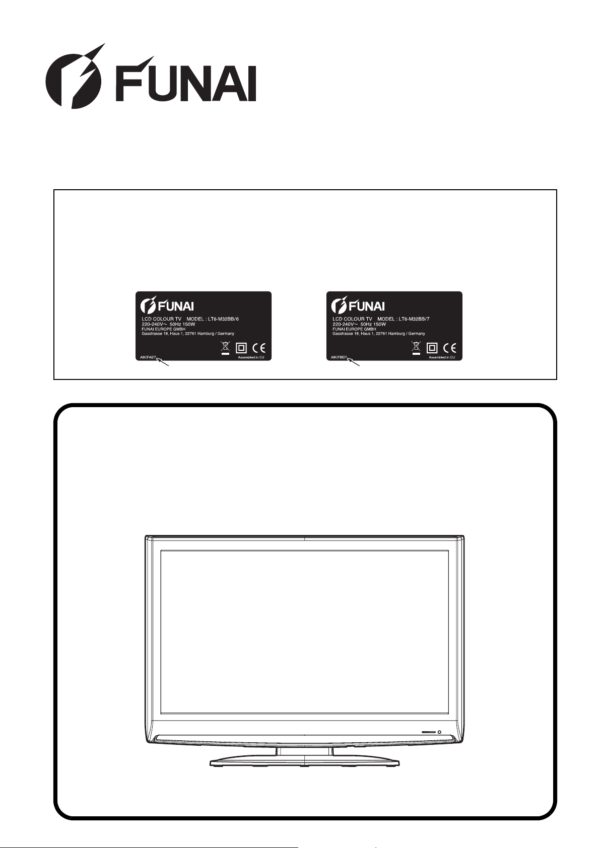
This Service Manual is for the
LT6-M32BB(A8CFAEP) / LT6-M32BB(A8CFBEP) model.
For the LT6-M32BB(A8CFAEP) / LT6-M32BB(A8CFBEP) model, the letter
(A8CFAEP) / (A8CFBEP) is printed on the Rating Label on the back of the
unit. Refer to the Rating Label below.
Rating Label
Rating Label
"A8CFAEP"
"A8CFBEP"
32″ COLOR LCD TELEVISION
LT6-M32BB
Page 2

32″ COLOR LCD TELEVISION
LT6-M32BB
TABLE OF CONTENTS
Specifications . . . . . . . . . . . . . . . . . . . . . . . . . . . . . . . . . . . . . . . . . . . . . . . . . . . . . . . . . . . . . . . . . . . . . . . . . . . 1-1
Important Safety Precautions . . . . . . . . . . . . . . . . . . . . . . . . . . . . . . . . . . . . . . . . . . . . . . . . . . . . . . . . . . . . . . . 2-1
Standard Notes for Servicing . . . . . . . . . . . . . . . . . . . . . . . . . . . . . . . . . . . . . . . . . . . . . . . . . . . . . . . . . . . . . . . 3-1
Cabinet Disassembly Instructions . . . . . . . . . . . . . . . . . . . . . . . . . . . . . . . . . . . . . . . . . . . . . . . . . . . . . . . . . . . 4-1
Electrical Adjustment Instructions . . . . . . . . . . . . . . . . . . . . . . . . . . . . . . . . . . . . . . . . . . . . . . . . . . . . . . . . . . . 5-1
How to Initialize the LCD Television. . . . . . . . . . . . . . . . . . . . . . . . . . . . . . . . . . . . . . . . . . . . . . . . . . . . . . . . . . 6-1
Block Diagrams . . . . . . . . . . . . . . . . . . . . . . . . . . . . . . . . . . . . . . . . . . . . . . . . . . . . . . . . . . . . . . . . . . . . . . . . . 7-1
Schematic Diagrams / CBA and Test Points . . . . . . . . . . . . . . . . . . . . . . . . . . . . . . . . . . . . . . . . . . . . . . . . . . . 8-1
Waveforms . . . . . . . . . . . . . . . . . . . . . . . . . . . . . . . . . . . . . . . . . . . . . . . . . . . . . . . . . . . . . . . . . . . . . . . . . . . . . 9-1
Wiring Diagram . . . . . . . . . . . . . . . . . . . . . . . . . . . . . . . . . . . . . . . . . . . . . . . . . . . . . . . . . . . . . . . . . . . . . . . . 10-1
Exploded View . . . . . . . . . . . . . . . . . . . . . . . . . . . . . . . . . . . . . . . . . . . . . . . . . . . . . . . . . . . . . . . . . . . . . . . . . 11-1
Mechanical Parts List . . . . . . . . . . . . . . . . . . . . . . . . . . . . . . . . . . . . . . . . . . . . . . . . . . . . . . . . . . . . . . . . . . . . 12-1
Electrical Parts List. . . . . . . . . . . . . . . . . . . . . . . . . . . . . . . . . . . . . . . . . . . . . . . . . . . . . . . . . . . . . . . . . . . . . . 13-1
The LCD panel is manufactured to provide many years of useful life.
Occasionally a few non active pixels may appear as a tiny spec of color.
This is not to be considered a defect in the LCD screen.
Page 3
SPECIFICATIONS
< TUNER >
VHF/UHF Input ----------- 75Ω unbal., IEC Connector
Center IF ------------------- SECAM-L 38.9MHz, SECAM-L’ 33.9MHz
Description Condition Unit Nominal Limit
1. Video S/N 80 dB --- 40
2. Audio S/N --- dB --- 40/40
< LCD PANEL >
Description Condition Unit Nominal Limit
1. Number of Pixels
2. Viewing Angle
<DVB-T>
Description Condition Unit Nominal Limit
1. RECEIVED
FREQ.RANGE
(-60dBm, 45ch.) *1
2. INPUT DYNAMIC
RANGE (mix./max) *1
3. C/N PERFORMANCE
*1
4 . M U LTI PAT H
a. Performance with
short delay echoes
b. Performance with
long delay echoes
c. C/N Performance on
0dB echo channel
(14µs)
Horizontal
Ver t i cal
Horizontal
Ver t i cal
+
-
VHF HIGH 7ch.
UHF 45ch.
VHF HIGH 7ch.
UHF 45ch.
UHF 45ch.
c:*2
d:*3
c:*2
d:*3
c:*1
pixels
pixels
kHz
kHz
dBm
dBm
dB
dB
dB
dB
dB
dB
dB
1366
768
°
°
-88 to 88
-88 to 88
1000
900
-82.5/2
-81.1/2
15
15
18.7
14.0
19.1
13.0
20.7
---
---
---
---
500
-150
-75/-10
-75/-10
≦18
≦18
≦23
≦20
≦23
≦18
≦24
*1: modulation parameters = [8k 64QAM CR=2/3 GI=1/32]
*2: modulation parameters = [2k 64QAM CR=2/3 GI=1/32]
*3: modulation parameters = [2k 16QAM CR=3/4 GI=1/32]
< VIDEO >
Description Condition Unit Nominal Limit
1. Over Scan
2. Color Temperature
3. Resolution
4. Brightness AT 100% WHITE FIELD cd/m
Horizontal
Ver t i cal
AT 70% WHITE FIELD
x
y
Horizontal
Ver t i cal
line
line
%
%
°K 12000
2
5
5
0.272
0.278
400
350
300 ---
±5
±5
--±0.005
±0.005
---
---
1-1 A8CFASP
Page 4

< AUDIO >
All items are measured across 16 Ω load at speaker output terminal.
Description Condition Unit Nominal Limit
1. Audio Output Power 10% THD: Lch/Rch W 5.0/5.0 4.0/4.0
2. Audio Distortion 500mW: Lch/Rch % 1.5/1.5 3.0/3.0
-
3. Audio Freq. Response
6dB: Lch
-
6dB: Rch
Hz
Hz
70 to 8 k
70 to 8 k
---
---
4. Audio S/N
Note: Nominal specifications represent the design specifications. All units should be able to approximate these.
Some will exceed and some may drop slightly below these specifications. Limit specifications represent
the absolute worst condition that still might be considered acceptable. In no case should a unit fail to meet
limit specifications.
VIDEO1
VIDEO2
dB
dB
---
---
>45/45
>45/45
1-2 A8CFASP
Page 5
IMPORTANT SAFETY PRECAUTIONS
Prior to shipment from the factory, our products are strictly inspected for recognized product safety and electrical
codes of the countries in which they are to be sold. However, in order to maintain such compliance, it is equally
important to implement the following precautions when a set is being serviced.
Safety Precautions for LCD TV
Circuit
1. Before returning an instrument to the
customer, always make a safety check of the
entire instrument, including, but not limited to, the
following items:
a. Be sure that no built-in protective devices are
defective and have been defeated during
servicing. (1) Protective shields are provided
on this chassis to protect both the technician
and the customer. Correctly replace all missing
protective shields, including any removed for
servicing convenience. (2) When reinstalling
the chassis and/or other assembly in the
cabinet, be sure to put back in place all
protective devices, including but not limited to,
nonmetallic control knobs, insulating
fishpapers, adjustment and compartment
covers/shields, and isolation resistor/capacitor
networks. Do not operate this instrument or
permit it to be operated without all
protective devices correctly installed and
functioning. Servicers who defeat safety
features or fail to perform safety checks
may be liable for any resulting damage.
b. Be sure that there are no cabinet openings
through which an adult or child might be able to
insert their fingers and contact a hazardous
voltage. Such openings include, but are not
limited to, (1) spacing between the LCD module
and the cabinet mask, (2) excessively wide
cabinet ventilation slots, and (3) an improperly
fitted and/or incorrectly secured cabinet back
cover.
c. Antenna Cold Check - With the instrument AC
plug removed from any AC source, connect an
electrical jumper across the two AC plug
prongs. Place the instrument AC switch in the
on position. Connect one lead of an ohmmeter
to the AC plug prongs tied together and touch
the other ohmmeter lead in turn to each tuner
antenna input exposed terminal screw and, if
applicable, to the coaxial connector. If the
measured resistance is less than 1.0 megohm
or greater than 5.2 megohm, an abnormality
exists that must be corrected before the
instrument is returned to the customer. Repeat
this test with the instrument AC switch in the off
position.
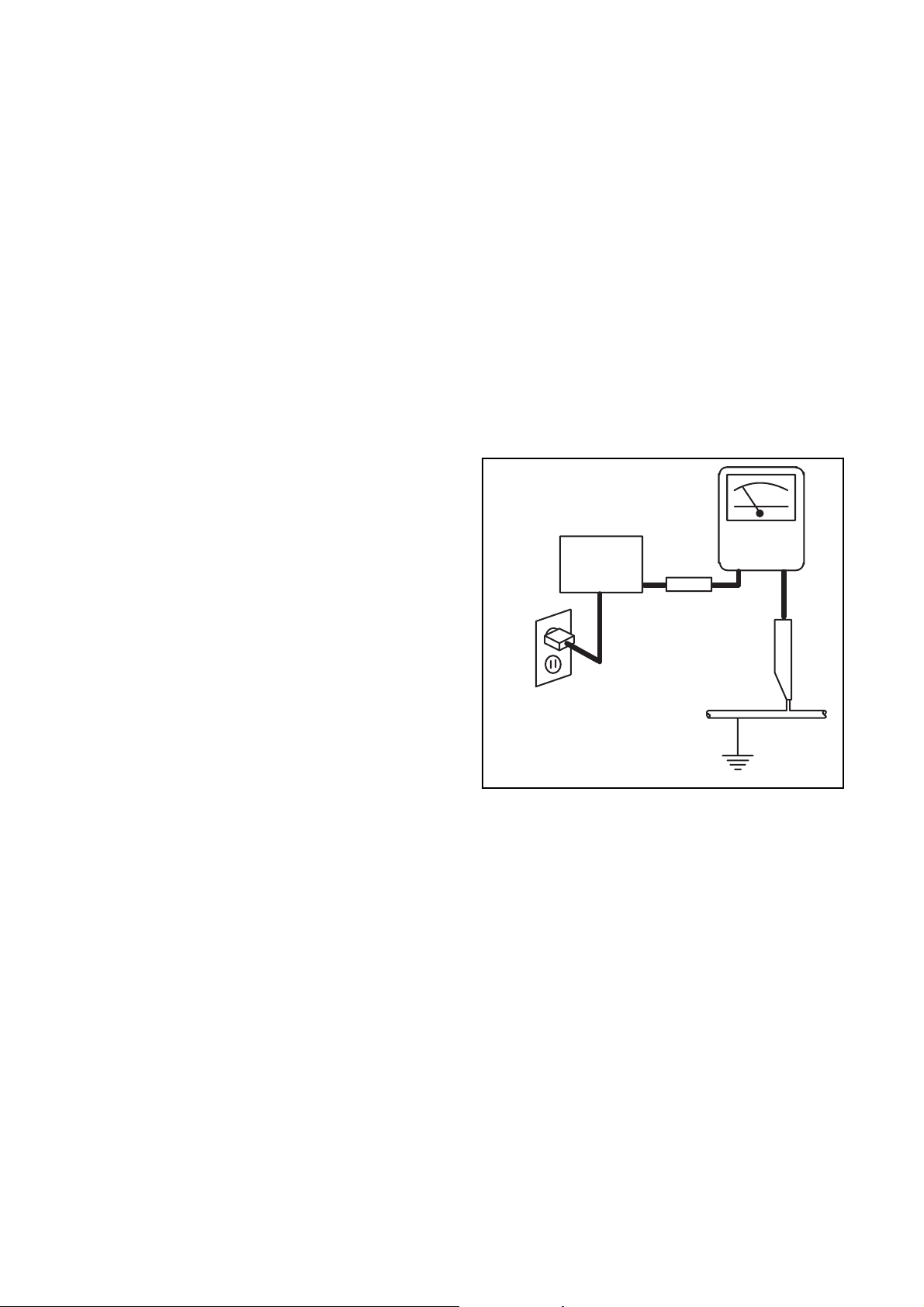
d. Leakage Current Hot Check - With the
instrument completely reassembled, plug the
AC line cord directly into a 230 V AC outlet. (Do
not use an isolation transformer during this
test.) Use a leakage current tester or a
metering system that complies with American
National Standards Institute (ANSI) C101.1
Leakage Current for Appliances and
Underwriters Laboratories (UL) 1410, (50.7).
With the instrument AC switch first in the on
position and then in the off position, measure
from a known earth ground (metal water pipe,
conduit, etc.) to all exposed metal parts of the
instrument (antennas, handle brackets, metal
cabinet, screw heads, metallic overlays, control
shafts, etc.), especially any exposed metal
parts that offer an electrical return path to the
chassis. Any current measured must not
exceed 0.5 milli-ampere. Reverse the
instrument power cord plug in the outlet and
repeat the test.
READING SHOULD
NOT BE ABOVE 0.5 mA
LEAKAGE
DEVICE
BEING
TESTED
TEST ALL EXPOSED
METAL SURFACES
ALSO TEST WITH
PLUG REVERSED
USING AC
ADAPTER PLUG
AS REQUIRED
ANY MEASUREMENTS NOT WITHIN THE
LIMITS SPECIFIED HEREIN INDICATE A
POTENTIAL SHOCK HAZARD THAT MUST
BE ELIMINATED BEFORE RETURNING THE
INSTRUMENT TO THE CUSTOMER OR
BEFORE CONNECTING THE ANTENNA OR
ACCESSORIES.
2. Read and comply with all caution and safety-
related notes on or inside the receiver cabinet, on
the receiver chassis, or on the LCD module.
3. Design Alteration Warning - Do not alter or add
to the mechanical or electrical design of this LCD
TV receiver. Design alterations and additions,
including, but not limited to circuit modifications
and the addition of items such as auxiliary audio
and/or video output connections, might alter the
safety characteristics of this receiver and create a
hazard to the user. Any design alterations or
additions will void the manufacturer's warranty and
may make you, the servicer, responsible for
personal injury or property damage resulting
therefrom.
CURRENT
TESTER
+
EARTH
GROUND
_
2-1 LTVP_ISP
Page 6

4. Hot Chassis Warning -
a. Some TV receiver chassis are electrically
connected directly to one conductor of the AC
power cord and maybe safety-serviced without
an isolation transformer only if the AC power
plug is inserted so that the chassis is
connected to the ground side of the AC power
source. To confirm that the AC power plug is
inserted correctly, with an AC voltmeter,
measure between the chassis and a known
earth ground. If a voltage reading in excess of
1.0 V is obtained, remove and reinsert the AC
power plug in the opposite polarity and again
measure the voltage potential between the
chassis and a known earth ground.
b. Some TV receiver chassis normally have 85V
AC(RMS) between chassis and earth ground
regardless of the AC plug polarity. This chassis
can be safety-serviced only with an isolation
transformer inserted in the power line between
the receiver and the AC power source, for both
personnel and test equipment protection.
c. Some TV receiver chassis have a secondary
ground system in addition to the main chassis
ground. This secondary ground system is not
isolated from the AC power line. The two
ground systems are electrically separated by
insulation material that must not be defeated or
altered.
5. Observe original lead dress. Take extra care to
assure correct lead dress in the following areas: a.
near sharp edges, b. near thermally hot parts-be
sure that leads and components do not touch
thermally hot parts, c. the AC supply, d. high
voltage, and, e. antenna wiring. Always inspect in
all areas for pinched, out of place, or frayed wiring.
Check AC power cord for damage.
6. Components, parts, and/or wiring that appear to
have overheated or are otherwise damaged
should be replaced with components, parts, or
wiring that meet original specifications.
Additionally, determine the cause of overheating
and/or damage and, if necessary, take corrective
action to remove any potential safety hazard.
7. Product Safety Notice - Some electrical and
mechanical parts have special safety-related
characteristics which are often not evident from
visual inspection, nor can the protection they give
necessarily be obtained by replacing them with
components rated for higher voltage, wattage, etc..
Parts that have special safety characteristics are
identified by a ! on schematics and in parts lists.
Use of a substitute replacement that does not
have the same safety characteristics as the
recommended replacement part might create
shock, fire, and/or other hazards. The product's
safety is under review continuously and new
instructions are issued whenever appropriate.
Prior to shipment from the factory, our products
are strictly inspected to confirm they comply with
the recognized product safety and electrical codes
of the countries in which they are to be sold.
However, in order to maintain such compliance, it
is equally important to implement the following
precautions when a set is being serviced.
2-2 LTVP_ISP
Page 7

Precautions during Servicing
A. Parts identified by the ! symbol are critical for
safety.
Replace only with part number specified.
B. In addition to safety, other parts and assemblies
are specified for conformance with regulations
applying to spurious radiation. These must also be
replaced only with specified replacements.
Examples: RF converters, RF cables, noise
blocking capacitors, and noise blocking filters, etc.
C. Use specified internal wiring. Note especially:
1) Wires covered with PVC tubing
2) Double insulated wires
3) High voltage leads
D. Use specified insulating materials for hazardous
live parts. Note especially:
1) Insulation Tape
2) PVC tubing
3) Spacers
4) Insulators for transistors.
E. When replacing AC primary side components
(transformers, power cord, etc.), wrap ends of
wires securely about the terminals before
soldering.
F. Observe that the wires do not contact heat
producing parts (heat sinks, oxide metal film
resistors, fusible resistors, etc.)
G. Check that replaced wires do not contact sharp
edged or pointed parts.
H. When a power cord has been replaced, check that
5~6 kg of force in any direction will not loosen it.
I. Also check areas surrounding repaired locations.
J. Use care that foreign objects (screws, solder
droplets, etc.) do not remain inside the set.
K. When connecting or disconnecting the internal
connectors, first, disconnect the AC plug from the
AC supply outlet.
L. When installing parts or assembling the cabinet
parts, be sure to use the proper screws and
tighten certainly.
2-3 LTVP_ISP
Page 8
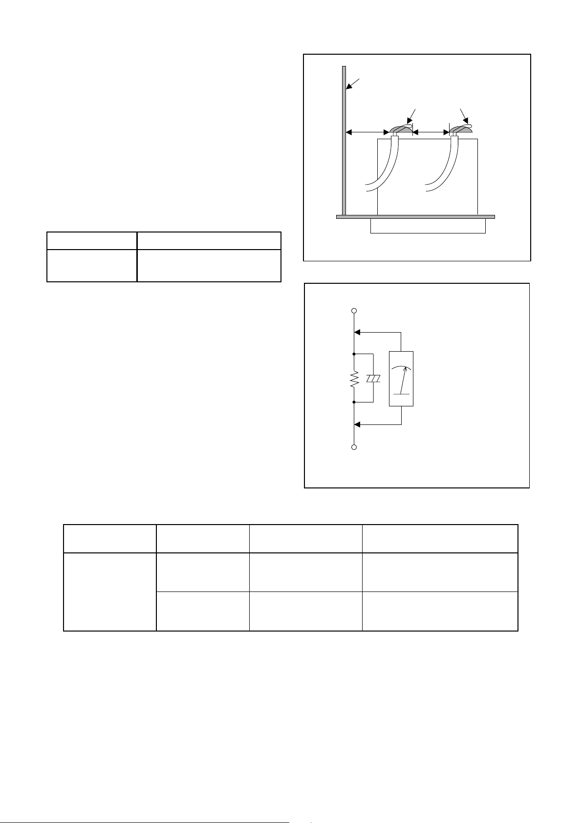
Safety Check after Servicing
Examine the area surrounding the repaired location
for damage or deterioration. Observe that screws,
parts and wires have been returned to original positions. Afterwards, perform the following tests and confirm the specified values in order to verify compliance
with safety standards.
1. Clearance Distance
When replacing primary circuit components, confirm
specified clearance distance (d) and (d') between soldered terminals, and between terminals and surrounding metallic parts. (See Fig. 1)
Table 1 : Ratings for selected area
AC Line Voltage Clearance Distance (d), (d’)
220 to 240 V
Note: This table is unofficial and for reference only.
Be sure to confirm the precise values.
≥ 3mm(d)
≥ 8mm(d’)
2. Leakage Current Test
Confirm the specified (or lower) leakage current between B (earth ground, power cord plug prongs) and
externally exposed accessible parts (RF terminals, antenna terminals, video and audio input and output terminals, microphone jacks, earphone jacks, etc.).
Chassis or Secondary Conductor
Primary Circuit
d' d
Exposed Accessible Part
Z
AC Voltmeter
(High Impedance)
Fig. 1
Measuring Method : (Power ON)
Insert load Z between B (earth ground, power cord
plug prongs) and exposed accessible parts. Use an
AC voltmeter to measure across both terminals of load
Z. See Fig. 2 and following table.
Table 2: Leakage current ratings for selected areas
AC Line Voltage Load Z Leakage Current (i)
2kΩ RES.
Connected in
parallel
220 to 240 V
50kΩ RES.
Connected in
parallel
Note: This table is unofficial and for reference only. Be sure to confirm the precise values.
i≤0.7mA AC Peak
i≤2mA DC
i≤0.7mA AC Peak
i≤2mA DC
One side of
B
Power Cord Plug Prongs
One side of power cord plug
prongs (B) to:
Antenna terminals
A/V Input, Output
Fig. 2
RF or
2-4 LTVP_ISP
Page 9
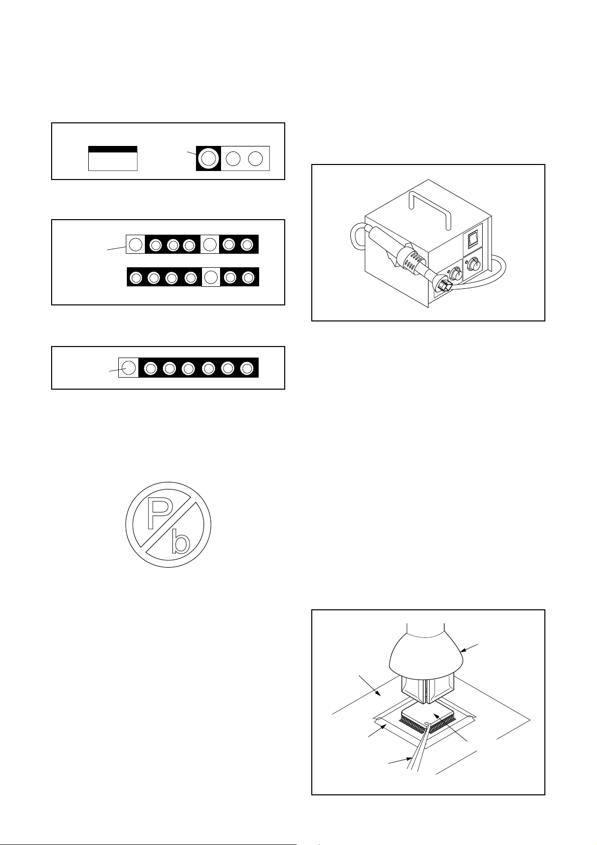
STANDARD NOTES FOR SERVICING
Circuit Board Indications
1. The output pin of the 3 pin Regulator ICs is
indicated as shown.
Top View
Out
2. For other ICs, pin 1 and every fifth pin are
indicated as shown.
Pin 1
3. The 1st pin of every male connector is indicated as
shown.
Pin 1
Input
In
Bottom View
5
10
Pb (Lead) Free Solder
Pb free mark will be found on PCBs which use Pb
free solder. (Refer to figure.) For PCBs with Pb free
mark, be sure to use Pb free solder. For PCBs
without Pb free mark, use standard solder.
Pb free mark
How to Remove / Install Flat Pack-IC
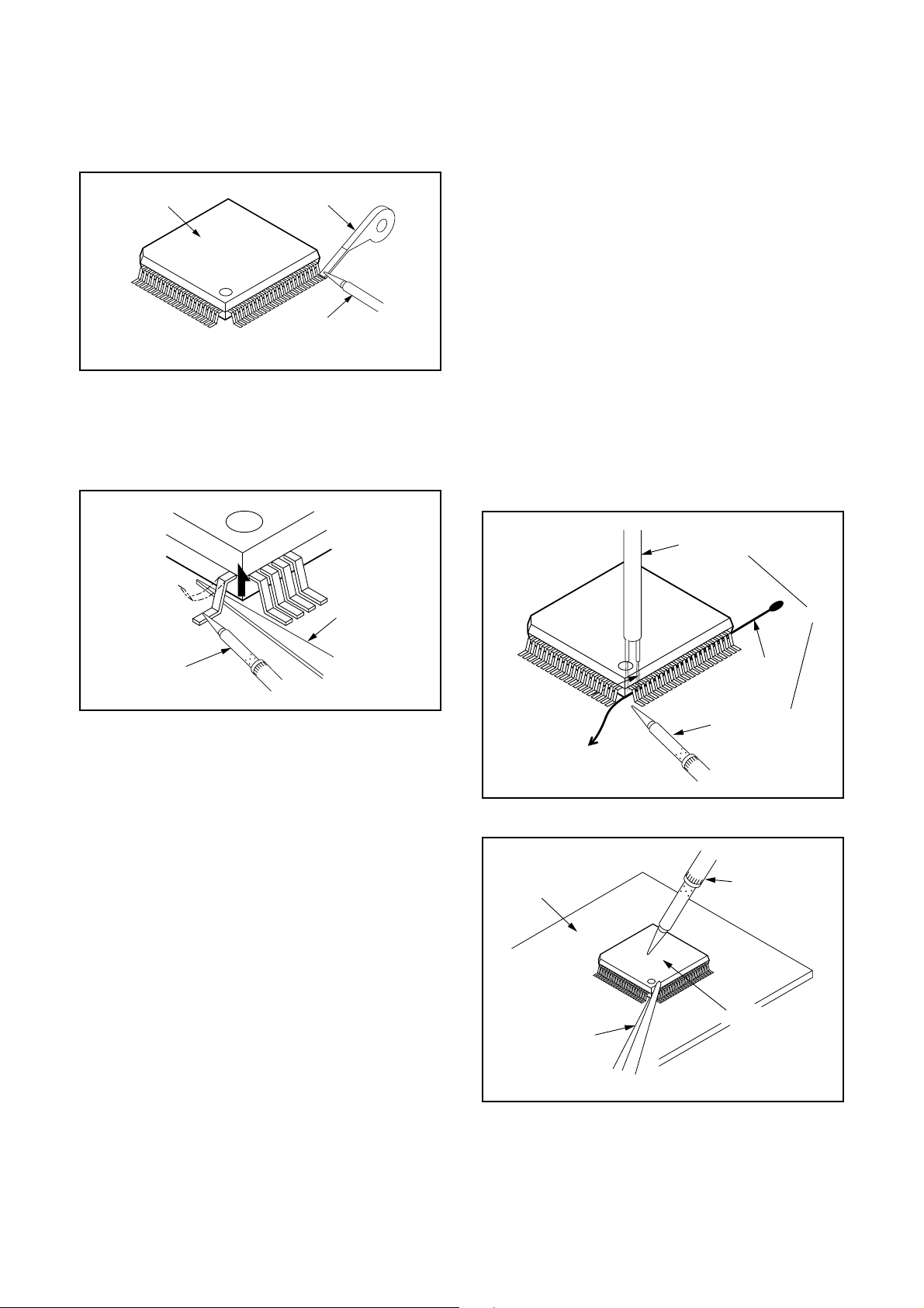
1. Removal
With Hot-Air Flat Pack-IC Desoldering Machine:
1. Prepare the hot-air flat pack-IC desoldering
machine, then apply hot air to the Flat Pack-IC
(about 5 to 6 seconds). (Fig. S-1-1)
Fig. S-1-1
2. Remove the flat pack-IC with tweezers while
applying the hot air.
3. Bottom of the flat pack-IC is fixed with glue to the
CBA; when removing entire flat pack-IC, first apply
soldering iron to center of the flat pack-IC and heat
up. Then remove (glue will be melted). (Fig. S-1-6)
4. Release the flat pack-IC from the CBA using
tweezers. (Fig. S-1-6)
CAUTION:
1. The Flat Pack-IC shape may differ by models. Use
an appropriate hot-air flat pack-IC desoldering
machine, whose shape matches that of the Flat
Pack-IC.
2. Do not supply hot air to the chip parts around the
flat pack-IC for over 6 seconds because damage
to the chip parts may occur. Put masking tape
around the flat pack-IC to protect other parts from
damage. (Fig. S-1-2)
3. The flat pack-IC on the CBA is affixed with glue, so
be careful not to break or damage the foil of each
pin or the solder lands under the IC when
removing it.
Hot-air
Flat Pack-IC
Desoldering
CBA
Masking
Tape
Tweezers
3-1 TVP_SN
Machine
Flat Pack-IC
Fig. S-1-2
Page 10
With Soldering Iron:
1. Using desoldering braid, remove the solder from
all pins of the flat pack-IC. When you use solder
flux which is applied to all pins of the flat pack-IC,
you can remove it easily. (Fig. S-1-3)
Flat Pack-IC
Desoldering Braid
Soldering Iron
Fig. S-1-3
2. Lift each lead of the flat pack-IC upward one by
one, using a sharp pin or wire to which solder will
not adhere (iron wire). When heating the pins, use
a fine tip soldering iron or a hot air desoldering
machine. (Fig. S-1-4)
With Iron Wire:
1. Using desoldering braid, remove the solder from
all pins of the flat pack-IC. When you use solder
flux which is applied to all pins of the flat pack-IC,
you can remove it easily. (Fig. S-1-3)
2. Affix the wire to a workbench or solid mounting
point, as shown in Fig. S-1-5.
3. While heating the pins using a fine tip soldering
iron or hot air blower, pull up the wire as the solder
melts so as to lift the IC leads from the CBA
contact pads as shown in Fig. S-1-5.
4. Bottom of the flat pack-IC is fixed with glue to the
CBA; when removing entire flat pack-IC, first apply
soldering iron to center of the flat pack-IC and heat
up. Then remove (glue will be melted). (Fig. S-1-6)
5. Release the flat pack-IC from the CBA using
tweezers. (Fig. S-1-6)
Note: When using a soldering iron, care must be
taken to ensure that the flat pack-IC is not
being held by glue. When the flat pack-IC is
removed from the CBA, handle it gently
because it may be damaged if force is applied.
Sharp
Pin
Fine Tip
Soldering Iron
3. Bottom of the flat pack-IC is fixed with glue to the
CBA; when removing entire flat pack-IC, first apply
soldering iron to center of the flat pack-IC and heat
up. Then remove (glue will be melted). (Fig. S-1-6)
4. Release the flat pack-IC from the CBA using
tweezers. (Fig. S-1-6)
Fig. S-1-4
To Solid
Mounting Point
CBA
Hot Air Blower
or
Iron Wire
Soldering Iron
Fig. S-1-5
Fine Tip
Soldering Iron
Flat Pack-IC
Tweezers
Fig. S-1-6
3-2 TVP_SN
Page 11
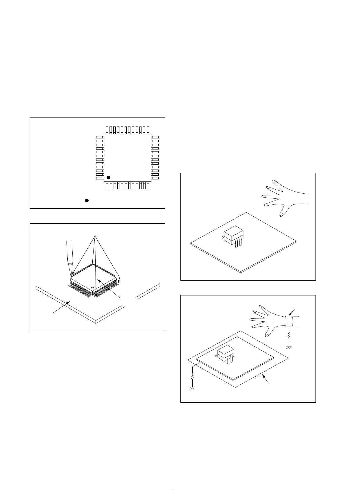
2. Installation
1. Using desoldering braid, remove the solder from
the foil of each pin of the flat pack-IC on the CBA
so you can install a replacement flat pack-IC more
easily.
2. The “●” mark on the flat pack-IC indicates pin 1.
(See Fig. S-1-7.) Be sure this mark matches the 1
on the PCB when positioning for installation. Then
presolder the four corners of the flat pack-IC. (See
Fig. S-1-8.)
3. Solder all pins of the flat pack-IC. Be sure that
none of the pins have solder bridges.
Example :
Pin 1 of the Flat Pack-IC
is indicated by a " " mark.
Fig. S-1-7
Instructions for Handling Semiconductors
Electrostatic breakdown of the semi-conductors may
occur due to a potential difference caused by
electrostatic charge during unpacking or repair work.
1. Ground for Human Body
Be sure to wear a grounding band (1 MΩ) that is
properly grounded to remove any static electricity that
may be charged on the body.
2. Ground for Workbench
Be sure to place a conductive sheet or copper plate
with proper grounding (1 MΩ) on the workbench or
other surface, where the semi-conductors are to be
placed. Because the static electricity charge on
clothing will not escape through the body grounding
band, be careful to avoid contacting semi-conductors
with your clothing.
<Incorrect>
CBA
Presolder
Flat Pack-IC
Fig. S-1-8
<Correct>
1MΩ
CBA
Grounding Band
1MΩ
CBA
Conductive Sheet or
Copper Plate
3-3 TVP_SN
Page 12
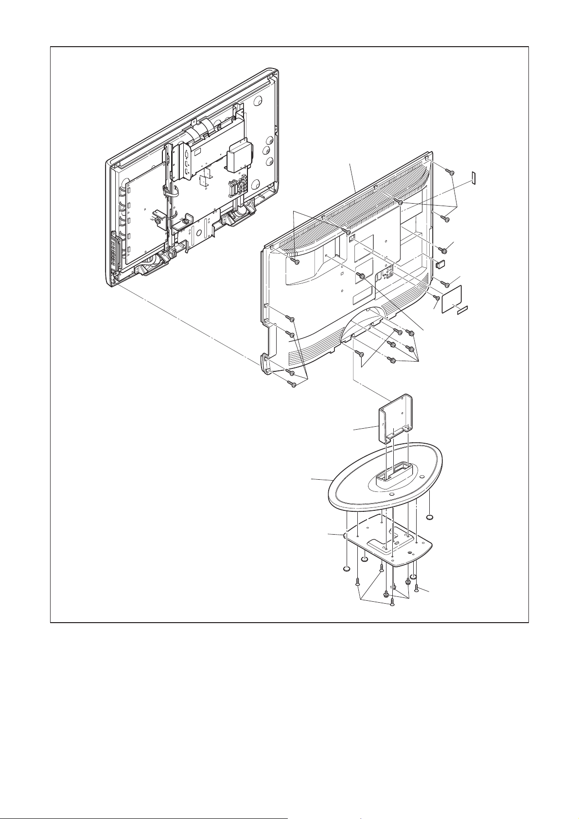
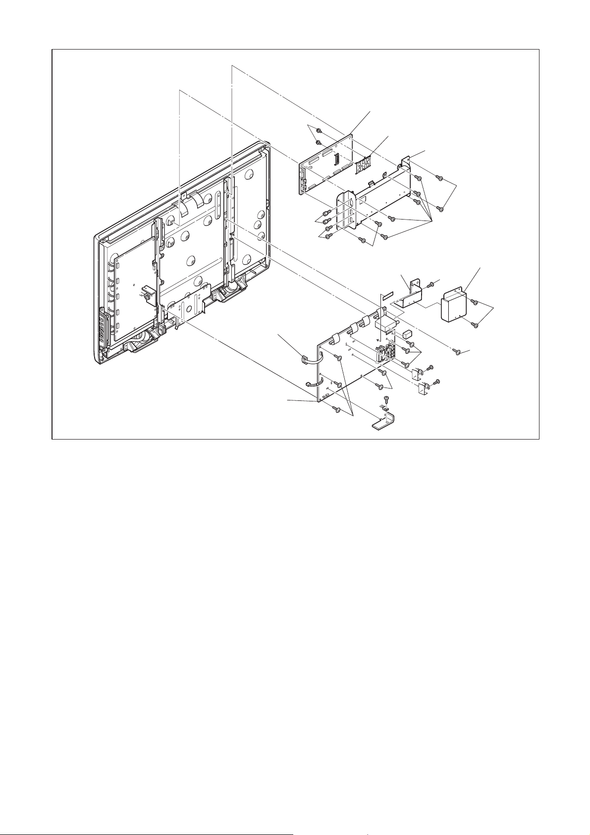
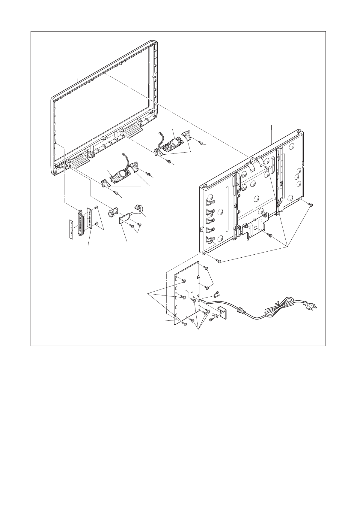
CABINET DISASSEMBLY INSTRUCTIONS
1. Disassembly Flowchart
This flowchart indicates the disassembly steps for the
cabinet parts, and the CBA in order to gain access to
item(s) to be serviced. When reassembling, follow the
steps in reverse order. Bend, route and dress the
cables as they were.
[15] Function CBA
[16] Speaker
Holder(s) [L,R]
[17] Speaker(s)
[13] Junction-A
CBA
[14] IR Sensor
CBA
[4] Rear Cabinet
[5] FFC Shield
[6] Shield Box
[7] Digital Main
CBA Unit
[8] Shield (T)
[9] Power Supply
CBA
[11] Inverter CBA
[12] LCD Module
Assembly
[18] Front Cabinet
[1] Stand Base
Plate
[2] Stand Cover
[3] Stand Hinge
[10] Junction-B
CBA
2. Disassembly Method
Removal
Step/
Loc.
Part
Fig.
No.
Stand Base
[1]
Plate
Stand
[2]
Cover
Stand
[3]
Hinge
Rear
[4]
Cabinet
[5] FFC Shield D2 2(S-7) ---
[6] Shield Box
Digital Main
[7]
CBA UnitD2D4
[8] Shield (T) D2 (S-12) ---
Remove/*Unhook/
No.
Unlock/Release/
Unplug/Unclamp/
Note
Desolder
D1 4(S-1), 3(S-2), 4(S-3) ---
D1 --------------- ---
D1 --------------- ---
D1 12(S-4), (S-5), 2(S-6) ---
2(S-8), 7(S-9),
4(S-10), *CN3601,
D2
*CN3701, *CN3704,
D4
*CN4501, *CN4502,
*CN4503
2(S-11), Connector IC
Card OSU
---
---
Removal
Step/
Loc.
No.
Part
Remove/*Unhook/
Fig.
No.
Unlock/Release/
Unplug/Unclamp/
Note
Desolder
[9]
[10]
[11]
Power
Supply
CBA
Junction-B
CBA
Inverter
CBA
9(S-13), *CN102,
D2
*CN801, *CN802,
D4
*CN1000, *CN1901
D2
*CN803B ---
D4
9(S-14), *CN1050,
D3
*CN1100, *CN1150,
D4
*CN1200, *CN1250
---
---
LCD
[12]
Module
D3 4(S-15) ---
Assembly
[13]
[14]
[15]
Junction-A
CBA
IR Sensor
CBA
Function
CBA
D3
*CL101B ---
D4
D3
2(S-16), *CL102A ---
D4
D3
2(S-17) ---
D4
Speaker
[16]
Holder(s)
D3 4(S-18) ---
[L,R]
[17] Speaker(s) D3 --------------- ---
Front
[18]
↓
(1)
Cabinet
↓
(2)
D3 --------------- ---
↓
(3)
↓
(4)
(5)
↓
Note:
(1) Order of steps in procedure. When reassembling,
follow the steps in reverse order. These numbers
are also used as the Identification (location) No. of
parts in figures.
(2) Parts to be removed or installed.
(3) Fig. No. showing procedure of part location
(4) Identification of parts to be removed, unhooked,
unlocked, released, unplugged, unclamped, or
desoldered.
N = Nut, L = Locking Tab, S = Screw,
CN = Connector
* = Unhook, Unlock, Release, Unplug, or Desolder
e.g. 2(S-2) = two Screws (S-2),
2(L-2) = two Locking Tabs (L-2)
(5) Refer to the following "Reference Notes in the
Ta bl e ."
4-1 A8CFADC
Page 13
[4] Rear Cabinet
(S-4)
[3] Stand Hinge
[2] Stand Cover
(S-4)
(S-6)
(S-4)
(S-5)
(S-6)
(S-1)
(S-4)
(S-4)
[1] Stand Base Plate
4-2 A8CFADC
(S-3)
(S-3)
(S-2)
Fig. D1
Page 14
(S-11)
[7] Digital Main CBA Unit
Connector IC Card OSU
[6] Shield Box
(S-10)
[10] Junction-B CBA
[9] Power Supply CBA
(S-8)
(S-9)
(S-10)
[8] Shield (T)
(S-13)
(S-13)
(S-9)
(S-13)
[5] FFC Shield
(S-12)
(S-7)
(S-13)
Fig. D2
4-3 A8CFADC
Page 15
[18] Front Cabinet
[17] Speaker
(S-17)
[15] Function
CBA
[17] Speaker
(S-18)
[16] Speaker
Holder(s) [L,R]
(S-18)
[13] Junction-A
CBA
(S-16)
[14] IR Sensor
CBA
(S-14)
[12] LCD Module Assembly
(S-18)
[16] Speaker
Holder(s) [L,R]
(S-18)
(S-15)
(S-14)
[11] Inverter CBA
(S-14)
Fig. D3
4-4 A8CFADC
Page 16
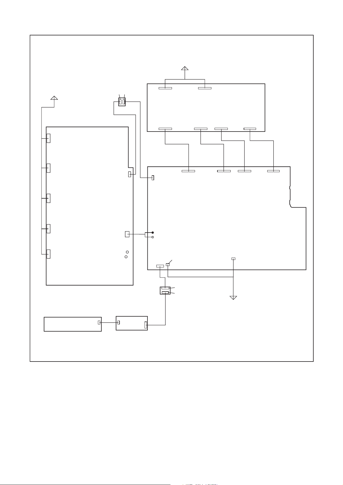
TV Cable Wiring Diagram
To LCD Module
Assembly
To LCD
Module
Assembly
Inverter CBA
CN1050
CN1100
CN1150
CN1200
CN804 CN803B
Junction-B
CBA
CN1901
CN1000
CN4501 CN4502
CN3601 CN3701 CN4503
Power Supply
CBA
CN803A
CLN400
CN104A CN101A CN102A CN103A
Digital Main
CBA Unit
CN3704
CN1250
Function CBA
CL102B
AC CORD
IR Sensor CBA
CL102A
CN102
Junction-A
CBA
CL101A
CN802
CN801
CN101
CL101B
To Speaker
Fig. D4
4-5 A8CFADC
Page 17
ELECTRICAL ADJUSTMENT INSTRUCTIONS
General Note: “CBA” is abbreviation for
“Circuit Board Assembly.”
Note: Electrical adjustments are required after
replacing circuit components and certain
mechanical parts. It is important to perform
these adjustments only after all repairs and
replacements have been completed.
Also, do not attempt these adjustments unless
the proper equipment is available.
Test Equipment Required
1. DC Voltmeter
2. Pattern Generato
3. Color Analyzer
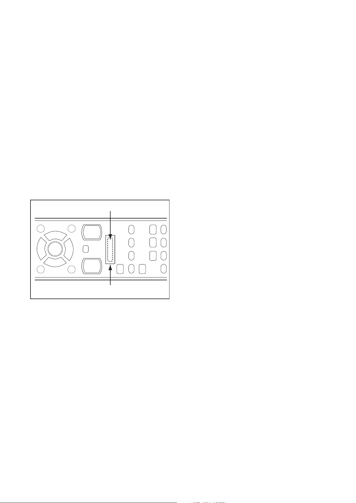
How to make the Service remote
control unit:
Cut “A” portion of the attached remote control unit as
shown in Fig. 1.
service button
How to set up the service mode:
Service mode:
1. Use the service remote control unit.
2. Turn the power on.
3. Press the service button on the service remote
control unit as shown in Fig.1.
A
Fig. 1
5-1 A8CFAEA
Page 18
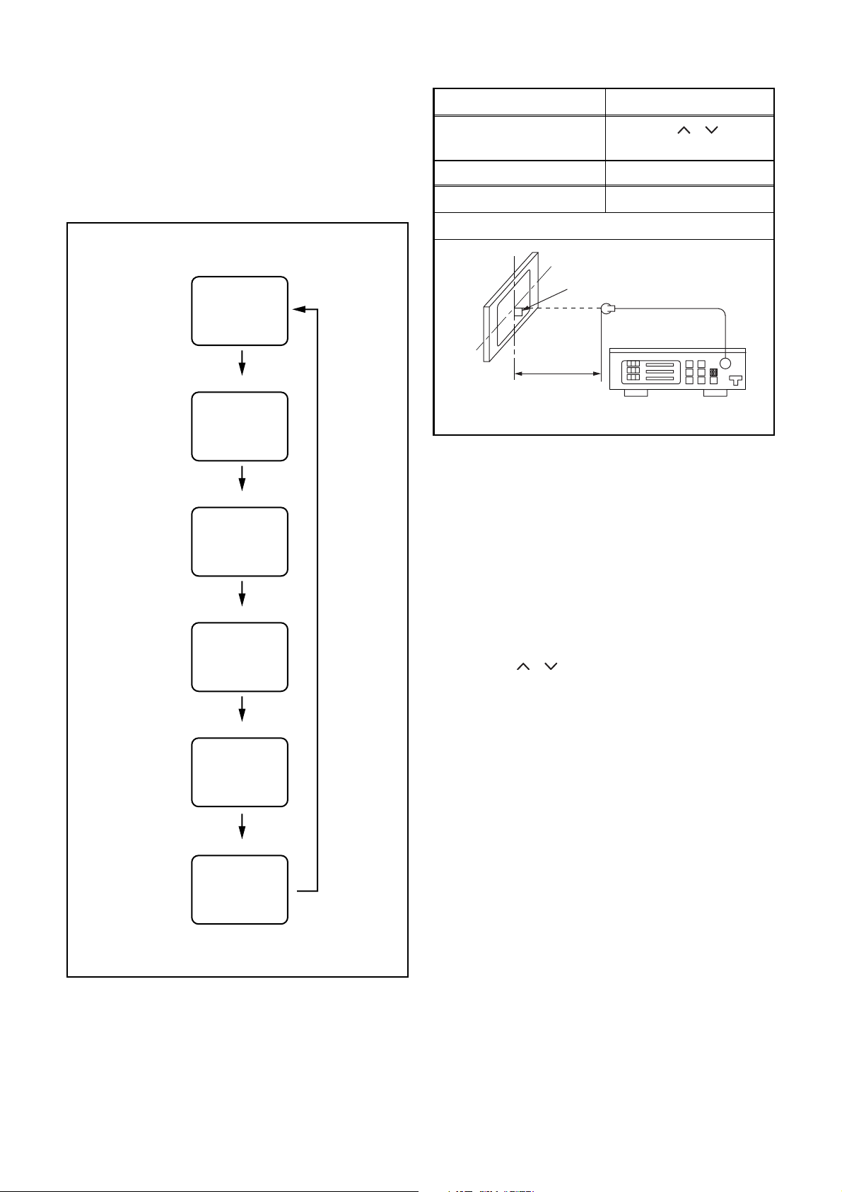
1. Purity Check Mode
2. VCOM Adjustment.
This mode cycles through full-screen displays of red,
green, blue, and white to check for non-active pixels.
1. Enter the Service mode.
2. Each time pressing [7] button on the service
remote control unit, the display changes as
follows.
Purity Check Mode
White mode
[7] button
[7] button
Black mode
[7] button
Red mode
[7] button
Green mode
[7] button
Blue mode
Test Point
Screen
Adj. Point
[P / ]
buttons
M. EQ. Spec.
Color analyzer
See below
Figure
It carries out in a darkroom.
Perpendicularity
L = 3 cm
Color Analyzer
1. Operate the unit for more than 20 minutes.
2. Set the color analyzer and bring the optical
receptor to the center on the LCD-Panel surface
after zero point calibration as shown above.
Note: The optical receptor must be set
perpendicularly to the LCD Panel surface.
3. Enter the Service mode.
4. [VCOM1]
Press [2] button on the service remote control unit.
[VCOM2]
Press [3] button on the service remote control unit.
5. Press [P / ] buttons on the service remote
control unit so that the color analyzer value
becomes minimum.
[7] button
White 20% mode
Note:
When entering this mode, the default setting is White mode.
5-2 A8CFAEA
Page 19
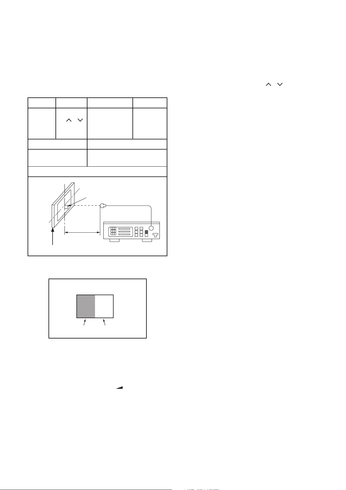
The following adjustment normally are not attempted in
the field. Only when replacing the LCD Panel then adjust
as a preparation.
3. White Balance Adjustment
Purpose: To mix red, green and blue beams correctly
for pure white.
Symptom of Misadjustment: White becomes bluish
or reddish.
Test Point
Screen
Adj. Point Mode Input
[P / ]
buttons
[VIDEO]
C/D
M. EQ. Spec.
White Raster
(APL 70%)
or
(APL 30%)
5. [CUTOFF]
Press [3] button to select “COB” for Blue Cutoff
adjustment. Press [1] button to select “COR” for
Red Cutoff adjustment.
[DRIVE]
Press [6] button to select “DB” for Blue Drive
adjustment. Press [4] button to select “DR” for Red
Drive adjustment.
6. In each color mode, press [P / ] buttons to
adjust the values of color.
7. Adjust Cutoff and Drive so that the color
temperature becomes 12000°K (x
=
0.272 / y
=
0.278 ±0.005).
Pattern Generator,
Color analyzer
x= 0.272 ± 0.005
y= 0.278 ± 0.005
Figure
It carries out in a darkroom.
Perpendicularity
L = 3 cm
INPUT: WHITE 70%, 30%
Color Analyzer
1. Operate the unit for more than 20 minutes.
2. Input the White Raster(70%=70IRE, 30%=30IRE).
INPUT SIGNAL
30%=30IRE
70%=70IRE
3. Set the color analyzer to the CHROMA mode and
bring the optical receptor to the center on the
LCD-Panel surface after zero point calibration as
shown above.
Note: The optical receptor must be set
perpendicularly to the LCD Panel surface.
4. Enter the Service mode. Press [ -] button on the
service remote control unit and select “C/D” mode.
5-3 A8CFAEA
Page 20

HOW TO INITIALIZE THE LCD TELEVISION
How to initialize the LCD television:
1. Turn the power on.
2. To enter the service mode, press the service
button on the service remote control unit. (Refer to
page 5-1.)
- To cancel the service mode, Press [ ] button on
the remote control unit.
3. Press [ ] button on the service remote control
unit to initialize the LCD television.
4. "INITIALIZED" will appear in the upper right of the
screen. "INITIALIZED" color will change to green
from red when initializing is complete.
6-1 A8CF0INT
Page 21
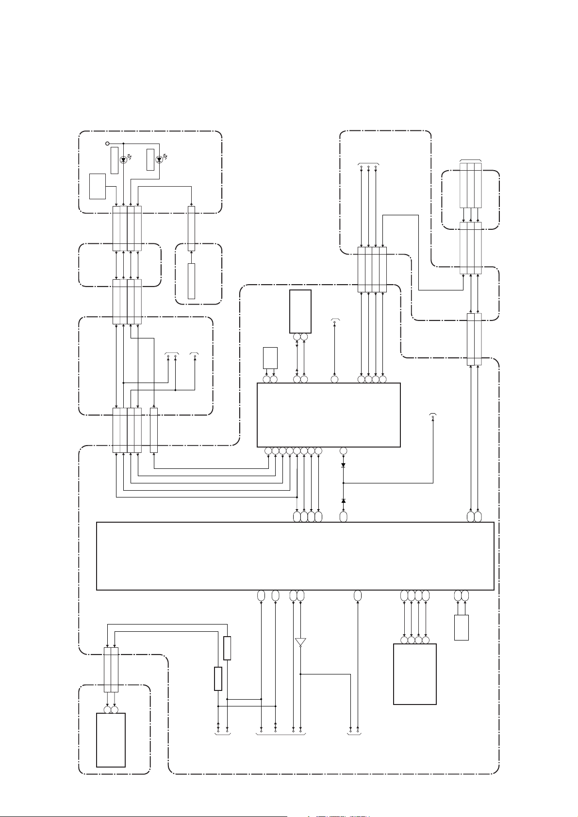
BLOCK DIAGRAMS
System Control Block Diagram
REMOTE
RCV101
+3.3V
D102
STANDBY
D101
SENSOR
CL101A
REMOTE22
CL101B
CN101
REMOTE52
CN102
CN104ACN3601
POWER
LED144
P-ON-H155
KEY-IN166KEY-IN116
JUNCTION-A
LED134
P-ON-H125
CN101A
CBA
CL102A
KEY-IN111
CL102B
KEY SWITCH
TO POWER
SUPPLY
BLOCK
DIAGRAM
TO AUDIO-2
BLOCK
DIAGRAM
P-ON-H1
P-ON-H2
P-ON-H2
TO
INVERTER
BLOCK
DIAGRAM
PROTECT3 1
CN803B CN804
PROTECT3
11332
CN803A
CN104ACN3601
2
2
BACKLIGHT-SW
3
BACKLIGHT-SW
(CN1000)
BACKLIGHT-ADJ3BACKLIGHT-SW
JUNCTION-B CBA
BACKLIGHT-ADJ
BACKLIGHT-ADJ
24223
TO POWER
SUPPLY
BLOCK
DIAGRAM
RESET
PROTECT1
IR SENSOR CBA
PROTECT2
POWER SUPPLY CBA
CN101ACN3701
PROTECT2
PROTECT3
PROTECT1
RESET
20 6
19 7
21 5
PROCESS
BLOCK
DIAGRAM
21
VCOM-PWM
17 9
3
22
RESET
PROTECT1
4
PROTECT223PROTECT3
TO AUDIO-2
BLOCK
DIAGRAM
FUNCTION CBAPOWER SUPPLY CBA
TO DIGITAL
SIGNAL
SDA
SCL
IC3102 (MEMORY)
5
6
VCOM-PWM
4MHz
OSC
X3101
6
XOUT
8
XIN
19
20
SCL
SDA
IC4513
(MAIN MICRO CONTROLLER)
CN4503CN102A
SCL18 8
45
SCL
REMOTE22 4
P-ON-H1125
P-ON-H213 13
SDA20 6
44
SDA
KEY-IN125 1
LED118 8
CN3701
BUFFER
Q3827
SDA
BUFFER
SCL
Q3828
(SUB MICRO CONTROLLER)
IC4700
SCL
SCL
AF12
LED1
12
SDA
KEY-IN1
24
SDA
AE12
P-ON-H2
13
REMOTE
RXD
P-ON-H1
TXD
11
14
15
16
P22
N22
R22
TXD1
RXD1
REMOTE
INPUT2
NICAM-RESET
B11
D12
Q3822
INPUT2
NICAM-RESET
RESET-MAIN
5
V24
RESET-MAIN
AMP-MUTE-SUB
18
AA2
AMP-MUTE-MAIN
S-SW
C12
INPUT2
S-SW
AMP-MUTE
A2
AC24
BACKLIGHT-SW
BACKLIGHT-ADJ
CLKOUT
X3301
U25
25MHz
OSC
CLKIN
U26
DIGITAL MAIN CBA UNIT
SPI-CLK
SPI-DO
SPI-DI
SPI-CS
Y25
Y24
W25
W24
652
1
SI
CS
SO
SCK
IC3706 (MEMORY)
IC200
(VIDEO/AUDIO SELECTOR)
POWER SUPPLY CBA
TO VIDEO
BLOCK
DIAGRAM
TO AUDIO-1
BLOCK
7-1
DIAGRAM
TO VIDEO
BLOCK
DIAGRAM
A8CFABLS
Page 22

Video Block Diagram
TO DIGITAL
SIGNAL
PROCESS
BLOCK
DIAGRAM
TO SYSTEM
CONTROL
BLOCK
DIAGRAM
TO DIGITAL
SIGNAL
PROCESS
BLOCK
DIAGRAM
TO SYSTEM
CONTROL
BLOCK
DIAGRAM
TO DIGITAL
SIGNAL
PROCESS
BLOCK
DIAGRAM
AUDIO SIGNAL
TS-DATA
VIDEO SIGNAL
IC3824 (DEMODULATOR)
58
DIF-OUT1
20 4
CN103A CN3704
SCL
13
MPEG2-TS
INTERFACES
DEMODULATOR
57
IF-AGC18 6
DIF-OUT2
22 2
25
SCL
SCL
64
SCL15 9
SDA
26
SDA
SDA2IF-AGC
63
SDA16 8
S-SW
TU-CVBS11 13
S-SW123
TU-VIDEO13 13
CN102A CN4503
WF1WF9
VIDEO
VIDEO-B
VIDEO-R
VIDEO-G
TU-CVBS
VIDEO-R323
VIDEO-B521
VIDEO-G422
VIDEO125
DTV-CVBS
WF7
WF8
4
IC3823
(INPUT SELECT)
5
3
SW CTL
INPUT2
109 11
COMP-Y
S-VIDEO-Y
S-VIDEO-C
COMP-Pr
COMP-Pb
DIGITAL MAIN CBA UNIT
S-VIDEO-Y23 3
S-VIDEO-C25 1
COMP-Y18 8
COMP-Pb20 6
COMP-Pr21 5
CN101A CN3701
WF6
WF3WF4 WF2
WF5
18
DIF-OUT1
TU501
(TUNER UNIT)
9
19
20
SCL
IF-AGC
DIF-OUT2
BUFFER
Q505
17
10SDA
VIDEO-OUT
IC200
JK204
(VIDEO SELECTOR)
16
VIDEO-IN1
42
3432332830
10
24
26
VIDEO
SELECTOR
14
12
CY
JK203
S-VIDEO-IN
636765
JK302
7-2
38
697371
20
RGB-
VIDEO-IN1
40
15
VIDEO-R1
7
11
VIDEO-B1
VIDEO-G1
19
JK301
VIDEO-OUT1
20
RGB-
VIDEO-IN2
15
11
VIDEO-R2
VIDEO-G2
7
19
VIDEO-B2
VIDEO-OUT2
JK202
COMPONENT
-Y-IN1
COMPONENT
-Pb-IN1
COMPONENT
-Pr-IN1
A8CFABLV
POWER SUPPLY CBA
Page 23

Audio-1 Block Diagram
TO
DIGITAL
SIGNAL
PROCESS
BLOCK
DIAGRAM
AUDIO SIGNAL
ACLK
BCLK
LRCLK
AD ATA 1
AUX-ADATA
111015
12
TO SYSTEM
CONTROL
BLOCK
DIAGRAM
INPUT2
BUFFER
Q3831
8
7
5
6
15
BUFFER
Q3832
14
IC3825
(AUDIO A/D CONVERTER)
IC200
(AUDIO SELECTOR)
(L-CH)
1
CN3704CN103A
AUDIO(L)321
WF10
99
93
85
A/D
CONVERTER
(R-CH)
2
AUDIO(R)420
1
97
AUDIO
SELECTOR
(L-CH)
81
79
757677
IC3822
(AUDIO D/A CONVERTER)
948682
98
AUDIO
(L-CH)
96
SELECTOR
D/A
15
100
(R-CH)
80
CONVERTER
(R-CH)
14
78
AMP-CTRL
62
CN4503CN102A
TU-AUDIO(L)10 16
109 11
SW CTL
IC3823
(INPUT SELECT)
1
2
13
12
DIGITAL MAIN CBA UNIT
24
(L-CH)
IC3821 (SOUND PROCESSOR)
22
(R-CH)
AUDIO SIGNAL
PROCESS
3
I2C BUS
I/F
19
18
SCL
SDA
RESET
21
NICAM-RESET
TU-AUDIO(R)11 15
TO AUDIO-2
BLOCK DIAGRAM
AMP-CTRL
JK204
AUDIO(L)
-IN1
AUDIO(R)
-IN1
JK206
COMPONENT
AUDIO(L)
-IN1
COMPONENT
AUDIO(R)
-IN1
JK205
PC-AUDIO-IN
JK302
6
RGB-AUDIO(L)
-IN12RGB-AUDIO(R)
-IN1
7-3
3
RGB-AUDIO(L)
-OUT1
1
RGB-AUDIO(R)
-OUT1
JK301
6
RGB-AUDIO(L)
-IN22RGB-AUDIO(R)
-IN2
3
RGB-AUDIO(L)
-OUT2
1
RGB-AUDIO(R)
-OUT2
TO SYSTEM
CONTROL
BLOCK
POWER SUPPLY CBA
CN3704CN103A
SIF915
6
SIF-OUT
TU501
(TUNER UNIT)
DIAGRAM
A8CFABLA1
Page 24

Audio-2 Block Diagram
SP801
SPEAKER
L-CH
CLN801
SP802
CLN802
SPEAKER
R-CH
JK303
HEADPHONE
JACK
AUDIO SIGNAL
IC801 (AUDIO POWER AMP)
IC702
+9V
(AMP)
SP(L)+2
CN801
8,9
PWM
3
SP(L)-1
18,19
GEN.
2
215
44,45
51
7
34,35
PWM
-1
6
GEN.
SP(R)-1
SP(R)+2
CN802
48 50
MUTE/STANDBY
CONTROL
Q802
Q304
IC300
(AMP)
AMP-CTRL
Q305
7
1
2
MUTE
5
3
TO AUDIO-1
BLOCK DIAGRAM
IC701
(AUDIO D/A CONVERTER)
(L-CH)
8
CN101ACN3701
LRCLK11 15
LRCLK
TO
DIGITAL
15
D/A
BCLK12 14
BCLK
AD ATA
SIGNAL
CONVERTER
PROCESS
14
(R-CH)
567
ACLK14 12
AD ATA13 13
AMP-MUTE917
ACLK
BLOCK
DIAGRAM
AMP-MUTE
TO SYSTEM
CONTROL
BLOCK
DIAGRAM
P-ON-H2
TO SYSTEM
CONTROL
BLOCK
DIAGRAM
7-4
DIGITAL MAIN CBA UNIT POWER SUPPLY CBA
A8CFABLA2
Page 25

Digital Signal Process Block Diagram
LCD MODULE
ASSEMBLY
BRSB2(+)52
BRSB2(-)51
BRSB1(+)50
BRSB1(-)49
BRSB0(+)48
BRSB0(-)47
BRSG2(+)46
BRSG2(-)45
BRSG1(+)44
BRSG1(-)43
BRSG0(+)42
BRSG0(-)41
BRSR2(+)17
BRSR2(-)16
BRSR1(+)15
BRSR1(-)14
BRSR0(+)13
BRSR0(-)12
BRSCLK(+)22
BRSCLK(-)21
VCOM7
STH-S11
TP119
POL18
STV5
FRSB2(+)53
FRSB2(-)52
FRSB1(+)51
VCOM9
CI
CARD
FRSB1(-)50
FRSB0(+)49
FRSB0(-)48
FRSG2(+)47
FRSG2(-)46
FRSG1(+)45
FRSG1(-)44
FRSG0(+)43
FRSG0(-)42
FRSR2(+)18
FRSR2(-)17
FRSR1(+)16
FRSR1(-)15
FRSR0(+)14
FRSR0(-)13
FRSCLK(+)23
FRSCLK(-)22
STH-F55
CPV6
OE15
STV7
TP120
POL19
VGH2
SLOT
CN4501
AUDIO SIGNAL
757473727170666564
VIDEO SIGNAL
IC4201(LCD DRIVE)
63
62616059585756556968907778
D-RSDS
OUTPUT
LVDS
RX
242522232021161718
AF20
AE20
AD19
AD20
AE19
AF19
AF18
AE18
AE21
19
AF21
81
LVDS
RX
9107856123
AF25
AF24
AE24
AE25
AD25
AD26
AD23
AD24
CN4502
52515049484744434140393837363534333246
D-RSDS
OUTPUT
DATA
MAPPING
4
(SDRAM)
DATA(0-15)
H1,H3,H7,H9
B1,B9,C2,C8,
F1,F9,G2,G8,
M2,M3,M7,M8,
D1,D3,D7,D9,
ADDESS(0-12)
N2,N3,N7,N8,
P2,P3,P7,P8,R2
AF26
IC3201
AE26
SWITCHING
83
DRIVE
IC4511,Q4511,
Q4512,Q4513
VCOM-PWM
TO SYSTEM
CONTROL
BLOCK
Q4501,Q4516
DIAGRAM
D(0-15)
IC3826 (LATCH)
A(8-13)
2,5,6,
LATCH
3,4,7,8,
13,14,
D(0-7)
A(0-13)
9,12,15
17,18
A(0-7)
145
808284
SCL
SDA
87
88
6
5
SCL
SDA
IC4202 (MEMORY)
IC4513 (DIGITAL SIGNAL PROCESS)
DIGITAL MAIN CBA UNIT
T4
Y3
TU-CVBS
T3
U4
COMP-Y
COMP-Pb
COMP-Pr
W3
VIDEO
S-VIDEO-Y
TO VIDEO
BLOCK
DIAGRAM
A/D
CONVERTER
SW
V3V4Y2
U3
S-VIDEO-C
Y1
VIDEO-R
VIDEO-G
AA1
VIDEO-B
JK3701
LVDS
T5
1
RED
TX
R4R3R5
3
2
BLUE
GREEN
VGA-HSYNC
K5
14
13
VSYNC
HSYNC
D-SUB
VGA-VSYNC
L5
IC3701 (MEMORY)
12
15
DATA
CLOCK
AB25
SDA
5
SCL
6
TS I/F
AB12
TS-DATA
TO VIDEO
DTV-CVBS
BLOCK
DIAGRAM
A13-15,A18,
A21-23,B13-15,
B17,B19-23
C15,C17-19,
C23,C24,D14,
D15,D17-19,
D22,D23
DIGITAL
SIGNAL
PROCESS
AUDIO I/F
AF15
AE15
AE16
AC17
AD15
AD ATA 1
AUX-ADATA
BCLK
TO AUDIO-1
BLOCK
ACLK
LRCLK
DIAGRAM
AD ATA
AD16
BCLK
LRCLK
TO AUDIO-2
BLOCK
ACLK
DIAGRAM
JK4001
AUDIO
DECODER
A9
B9
C8
TMDS-D0(+)
TMDS-D0(-)
TMDS-D1(+)
79461
B8
A8
C9
TMDS-D1(-)
TMDS-D2(+)
TMDS-D2(-)
3
HDMI-IN1
E9
B10
A10
C10
BUFFER
Q4002
BUFFER
SDA
SCL
TMDS-CLOCK(+)
TMDS-CLOCK(-)
101216
15
VIDEO
DECODER
HDMI
Q4001
I/F
JK4002
A5
B5
C4
TMDS-D0(+)
TMDS-D0(-)
TMDS-D1(+)
79461
Y22,Y23,AA21-23,
AB21-23,AF7-11,
AE9,AE10,AD10
B4A4B6
C5
TMDS-D1(-)
TMDS-D2(+)
HDMI-IN2
A6D7B7
Q4004
TMDS-D2(-)
TMDS-CLOCK(+)
TMDS-CLOCK(-)
SDA
3
101216
V21,W21,Y21,
AA20,AC20,AC21
AE14,AF14
Q4003
BUFFER
BUFFER
SCL
15
7-5
A8CFABLD
Page 26

Inverter Block Diagram
BACK
LIGHT
BACK
LIGHT
BACK
LIGHT
BACK
LIGHT
BACK
LIGHT
LCD MODULE
ASSEMBLY
CN1050
T1050
Q1100,
Q1101
1
2
786
3
2
DRIVE
1
2
CN1100
5
4
1
T1100
Q1102,
Q1103
786
3
2
DRIVE
4
1
5
1
2
CN1150
5
4
23
2
T1150
2
786
3
1
1
2
CN1200
5
4
T1200
2
13
786
3
12
16
1
1
2
CN1250
IS
VS
OVP
5
4
T1250
2
786
3
5
4
1
Q1020
DRIVE
DRIVE
DRIVE
IC1001
(INVERTER CONTROL)
10
NOTE:
The voltage for parts in hot circuit is measured using
hot GND as a common terminal.
HOT CIRCUIT. BE CAREFUL.
11
23457
T1951
ACL
HOT-GND
TO
POWER
SUPPLY
BLOCK
DIAGRAM
14
15
8
IC1930
SWITCHING
Q1930
14
DRIVE
3 2
Q1932
Q1970
IC1931
14
Q1931
LOGICLOGIC
3 2
HOT
CONTROL
INVERTER
11
19
COLD
213
4
VCC
IC1500 (COMPARATOR)
Q1971
213
6
6
5
13
12
4
VCC
5
9
10
13
12
INVERTER CBA
7
14
Q1972
IC1550 (COMPARATOR)
8
Q1002
CN1000
PROTECT31
TO SYSTEM
CONTROL
BLOCK
7
BACKLIGHT-ADJ3BACKLIGHT-SW
2
DIAGRAM
(CN804)
14
7-6
A8CFABLINV
Page 27

Power Supply Block Diagram
NOTE:
The voltage for parts in hot circuit is measured using
hot GND as a common terminal.
CAUTION !
For continued protection against fire hazard,
replace only with the same type fuse.
LCD+24.5V
LCD-6.8V
LCD+13V
P-ON+3.3V
+3.5V
+3.0V
LCD+3.3V
AL+3.3V
P-ON+5V
P-ON+9V
18
LCD+24.5V8
CN104A CN3601
16
LCD-6.8V10
9-11
19-21
LCD+13V5-7
P-ON+3.3V
15-17
2-4
+3.5V
22-24
7,8
+3.0V
18,19
JS652
14
LCD+3.3V12
Q646
AL+3.3V323P-ON+5V1,2
CN101A CN3701
SW-6.8V
24,25
12
P-ON+9V14
CN102A CN4503
Q600
DIGITAL MAIN CBA UNIT
P-ON-H1
P-ON-H2
TO SYSTEM
CONTROL
BLOCK
DIAGRAM
PROTECT2
PROTECT1
RESET
AL+13V
P-ON+9V
+35V
P-ON+5V
AL+3.3V
SW+3.3V
Q638,D634
SWITCHING
Q639,Q671
Q601
RESET
Q637
SW+5V
IC637
23
+3.3V
REG.
11
3
T400
CLN400
HOT-GND 2
ACL 1
3
1
CN1901
BRIDGE
RECTIFIER
D1901 - D1904
LINE
FILTER
L1902
LINE
FILTER
L1901
SWITCHING
Q632,Q634
14
T1902
SW+13V
Q645,D648
12
17
18
5
SW+9V
Q602
FEED
13
16
7
19
15
14
9
8
IC603
BACK
Q631
3 2
Q633
JS651
Q650
+5V REG.
COLD
HOT
HOT-GND
HOT
CONTROL
Q401
SWITCHING
SWITCHING
Q400
POWER SUPPLY CBA
INVERTER CBA
5
8
2
11
ACL
HOT CIRCUIT. BE CAREFUL.
CAUTION !
Fixed voltage (or Auto voltage selectable) power supply circuit is used in this unit.
If Main Fuse (F1901) is blown , check to see that all components in the power supply
circuit are not defective before you connect the AC plug to the AC power supply.
Otherwise it may cause some components in the power supply circuit to fail.
F1901
AC1901
AC CORD
T4A H 250V
TO
INVERTER
BLOCK
DIAGRAM
7-7
A8CFABLP
Page 28

SCHEMATIC DIAGRAMS / CBA AND TEST POINTS
Standard Notes
WARNING
Many electrical and mechanical parts in this chassis
have special characteristics. These characteristics
often pass unnoticed and the protection afforded by
them cannot necessarily be obtained by using
replacement components rated for higher voltage,
wattage, etc. Replacement parts that have these
special safety characteristics are identified in this
manual and its supplements; electrical components
having such features are identified by the mark “!” in
the schematic diagram and the parts list. Before
replacing any of these components, read the parts list
in this manual carefully. The use of substitute
replacement parts that do not have the same safety
characteristics as specified in the parts list may create
shock, fire, or other hazards.
Notes:
1. Do not use the part number shown on these
drawings for ordering. The correct part number is
shown in the parts list, and may be slightly
different or amended since these drawings were
prepared.
2. All resistance values are indicated in ohms
(K = 10
3. Resistor wattages are 1/4W or 1/6W unless
otherwise specified.
4. All capacitance values are indicated in µF
(P = 10
5. All voltages are DC voltages unless otherwise
specified.
3
, M = 106).
-6
µF).
8-1 A8CF0_SC
Page 29

LIST OF CAUTION, NOTES, AND SYMBOLS USED IN THE SCHEMATIC DIAGRAMS ON
THE FOLLOWING PAGES:
1. CAUTION:
FOR CONTINUED PROTECTION AGAINST FIRE HAZARD, REPLACE ONLY WITH THE SAME TYPE
FUSE.
2. CAUTION:
Fixed Voltage (or Auto voltage selectable) power supply circuit is used in this unit.
If Main Fuse (F1901) is blown, first check to see that all components in the power supply circuit are not
defective before you connect the AC plug to the AC power supply. Otherwise it may cause some components
in the power supply circuit to fail.
3. Note:
1. Do not use the part number shown on the drawings for ordering. The correct part number is shown in the
parts list, and may be slightly different or amended since the drawings were prepared.
2. To maintain original function and reliability of repaired units, use only original replacement parts which are
listed with their part numbers in the parts list section of the service manual.
4. Voltage indications on the schematics are as shown below:
Plug the TV power cord into a standard AC outlet.:
2
(Unit: Volt)
1
5.0 5.0
3
Power on mode
5. How to read converged lines
1-D3
Distinction Area
Line Number
(1 to 3 digits)
Examples:
1. "1-D3" means that line number "1" goes to the line number
"1" of the area "D3".
2. "1-B1" means that line number "1" goes to the line number
"1" of the area "B1".
6. Test Point Information
: Indicates a test point with a jumper wire across a hole in the PCB.
: Used to indicate a test point with a component lead on foil side.
: Used to indicate a test point with no test pin.
: Used to indicate a test point with a test pin.
Voltage
Indicates that the voltage
is not consistent here.
3
2
1
AREA D3
1-B1
AREA B1
1-D3
ABCD
8-2 A8CF0_SC
Page 30

Power Supply 1/4 Schematic Diagram
NOTE:
The voltage for parts in hot circuit is measured using
hot GND as a common terminal.
8-3
A8CFASCP1
Page 31

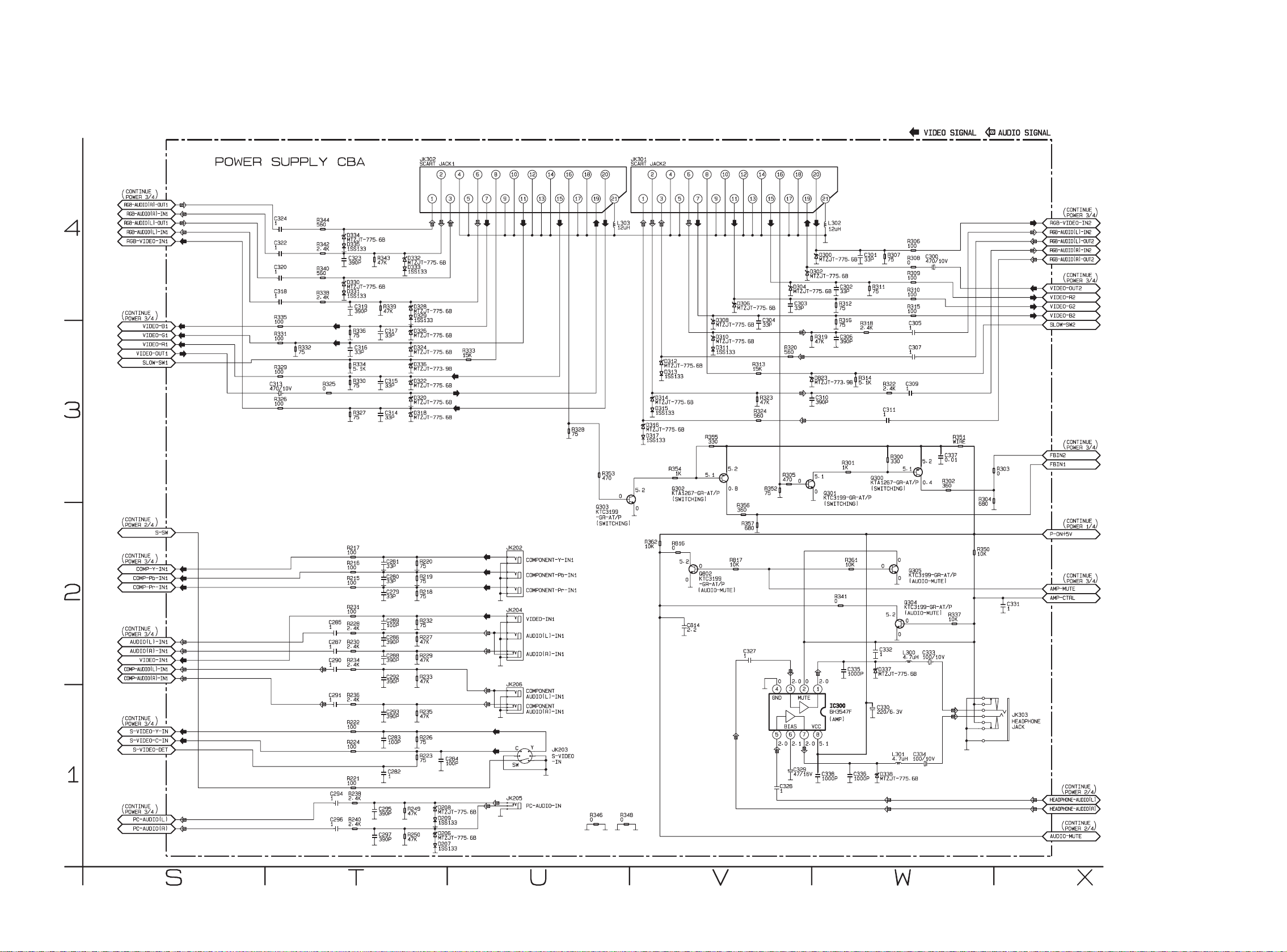
Power Supply 2/4 Schematic Diagram
8-4
A8CFASCP2
Page 32

Power Supply 3/4 Schematic Diagram
8-5
A8CFASCP3
Page 33
Power Supply 4/4 Schematic Diagram
8-6 A8CFASCP4
Page 34

Inverter & Junction-B Schematic Diagram
CAUTION !
For continued protection against fire hazard,
replace only with the same type fuse.
CAUTION !
Fixed voltage (or Auto voltage selectable) power supply circuit is used in this unit.
If Main Fuse (F1901) is blown , check to see that all components in the power supply
circuit are not defective before you connect the AC plug to the AC power supply.
Otherwise it may cause some components in the power supply circuit to fail.
NOTE:
The voltage for parts in hot circuit is measured using
hot GND as a common terminal.
8-7
A8CFASCINV
Page 35

Function Schematic Diagram
8-8
A8CFASCF
Page 36
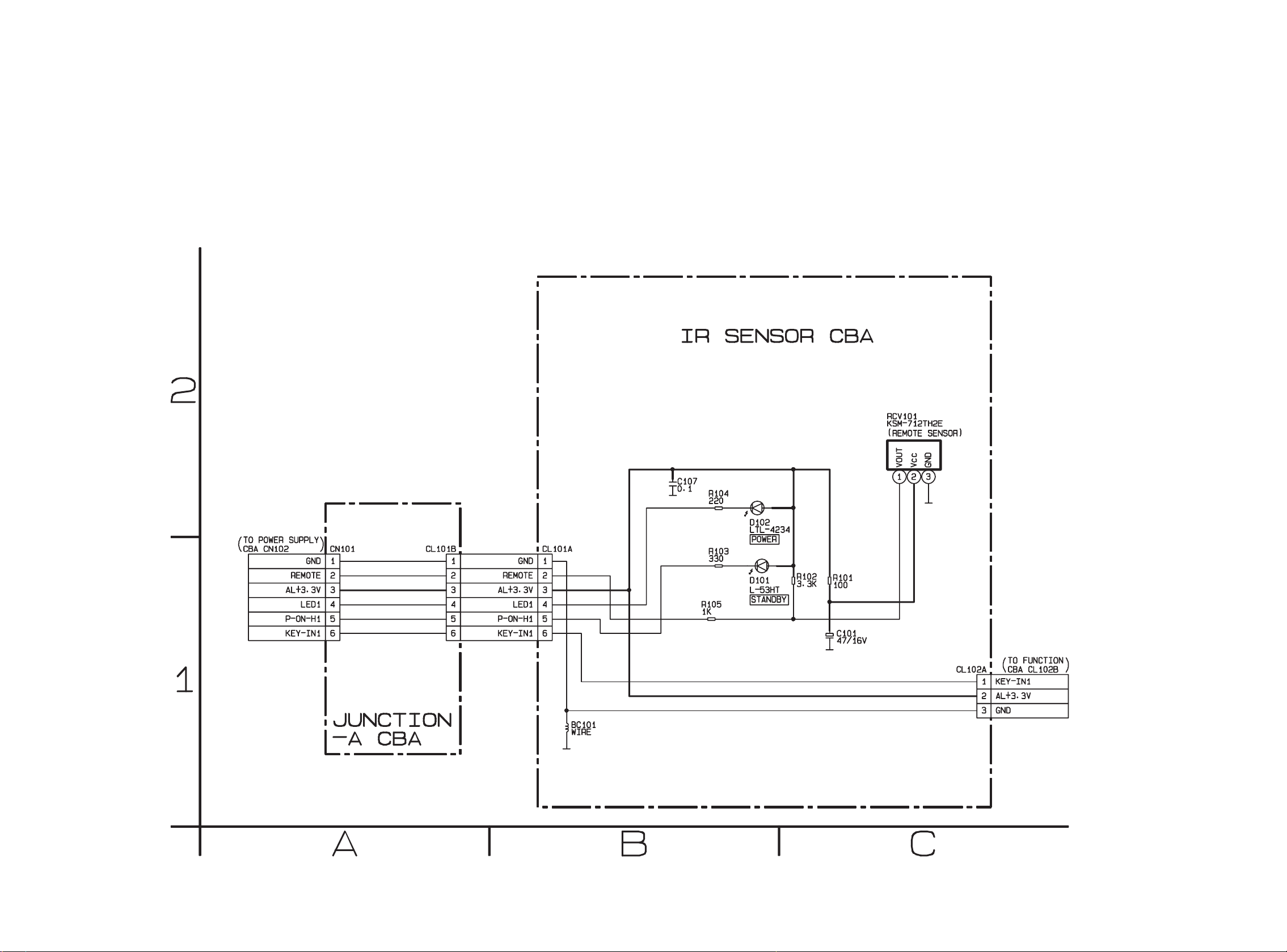
IR Sensor & Junction-A Schematic Diagram
8-9
A8CFASCIR
Page 37

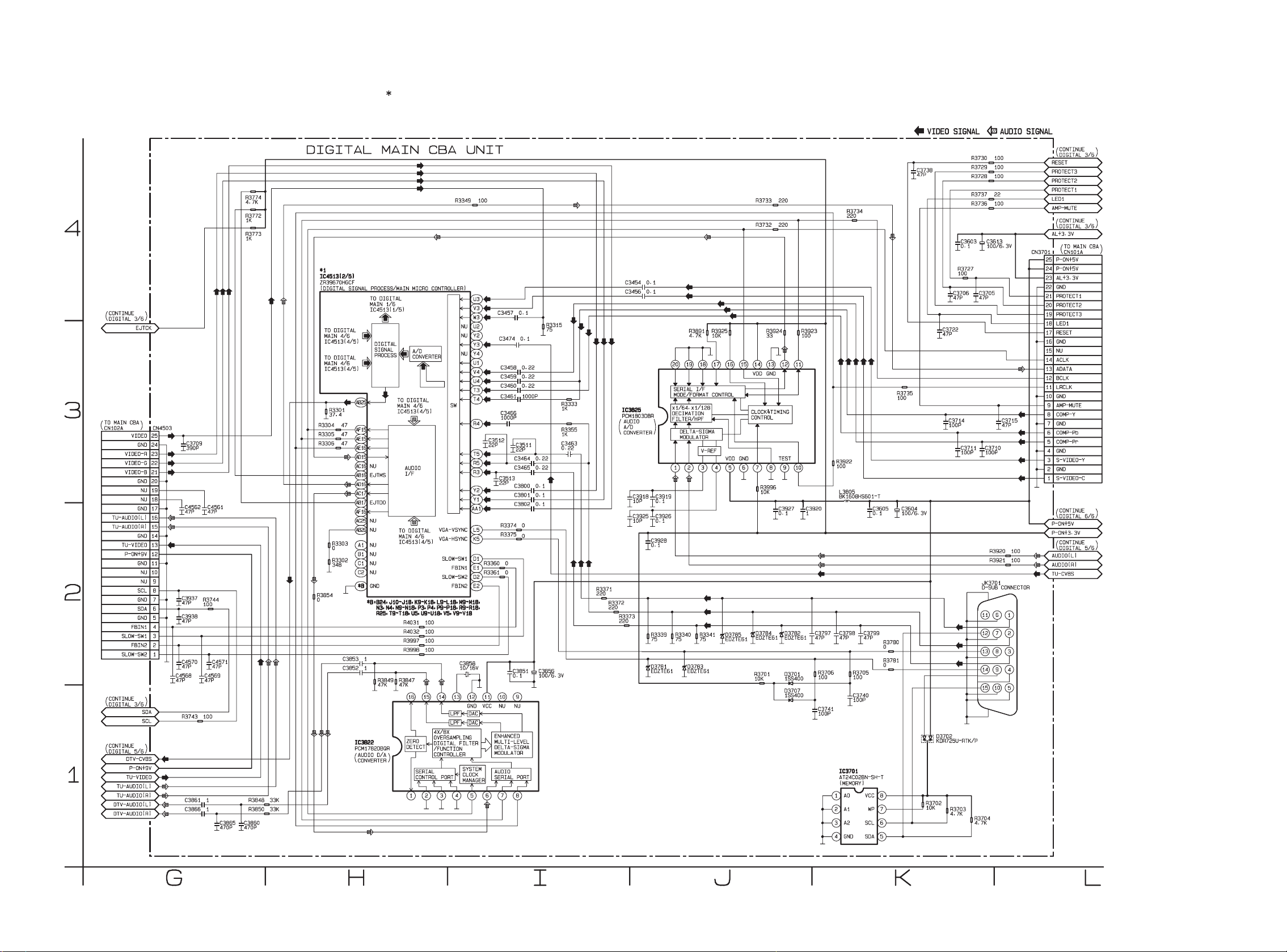
Digital Main 1/6 Schematic Diagram
1 NOTE:
The order of pins shown in this diagram is different from that of actual IC4513.
IC4513 is divided into seven and shown as IC4513 (1/5) ~ IC4513 (4/5) in this Digital Main Schematic Diagram Section.
8-10
A8CFASCD1
Page 38
Digital Main 2/6 Schematic Diagram
1 NOTE:
The order of pins shown in this diagram is different from that of actual IC4513.
IC4513 is divided into seven and shown as IC4513 (1/5) ~ IC4513 (4/5) in this Digital Main Schematic Diagram Section.
8-11
A8CFASCD2
Page 39

Digital Main 3/6 Schematic Diagram
1 NOTE:
The order of pins shown in this diagram is different from that of actual IC4513.
IC4513 is divided into seven and shown as IC4513 (1/5) ~ IC4513 (4/5) in this Digital Main Schematic Diagram Section.
8-12
A8CFASCD3
Page 40

Digital Main 4/6 Schematic Diagram
1 NOTE:
The order of pins shown in this diagram is different from that of actual IC4513.
IC4513 is divided into seven and shown as IC4513 (1/5) ~ IC4513 (4/5) in this Digital Main Schematic Diagram Section.
8-13
A8CFASCD4
Page 41

Digital Main 5/6 Schematic Diagram
8-14
A8CFASCD5
Page 42

Digital Main 6/6 Schematic Diagram
1 NOTE:
The order of pins shown in this diagram is different from that of actual IC4513.
IC4513 is divided into seven and shown as IC4513 (1/5) ~ IC4513 (4/5) in this Digital Main Schematic Diagram Section.
8-15
A8CFASCD6
Page 43

Power Supply CBA Top View
Because a hot chassis ground is present in the power
supply circut, an isolation transformer must be used.
Also, in order to have the ability to increase the input
slowly, when troubleshooting this type power supply
circuit, a variable isolation transformer is required.
NOTE:
The voltage for parts in hot circuit is measured using
hot GND as a common terminal.
8-16
BA8CF0F01013-1
Page 44

Power Supply CBA Bottom View
Because a hot chassis ground is present in the power
supply circut, an isolation transformer must be used.
Also, in order to have the ability to increase the input
slowly, when troubleshooting this type power supply
circuit, a variable isolation transformer is required.
NOTE:
The voltage for parts in hot circuit is measured using
hot GND as a common terminal.
WF10
PIN 3 OF
CN103A
WF7
PIN 5 OF
CN102A
WF8
PIN 4 OF
CN102A
WF9
PIN 3 OF
CN102A
WF1
PIN 1 OF
CN102A
WF3
PIN 25 OF
CN101A
WF2
PIN 23 OF
CN101A
WF6
PIN 21 OF
CN101A
WF5
PIN 20 OF
CN101A
WF4
PIN 18 OF
CN101A
8-17
BA8CF0F01013-1
Page 45

Inverter CBA Top View
NOTE:
The voltage for parts in hot circuit is measured using
hot GND as a common terminal.
CAUTION !
Fixed voltage (or Auto voltage selectable) power supply circuit is used in this unit.
If Main Fuse (F1901) is blown , check to see that all components in the power supply
circuit are not defective before you connect the AC plug to the AC power supply.
Otherwise it may cause some components in the power supply circuit to fail.
CAUTION !
For continued protection against fire hazard,
replace only with the same type fuse.
Because a hot chassis ground is present in the power
supply circuit, an isolation transformer must be used.
Also, in order to have the ability to increase the input
slowly,when troubleshooting this type power supply
circuit, a variable isolation transformer is required.
8-18
BA8CF0F01022
Page 46

Inverter CBA Bottom View
NOTE:
The voltage for parts in hot circuit is measured using
hot GND as a common terminal.
CAUTION !
For continued protection against fire hazard,
replace only with the same type fuse.
CAUTION !
Fixed voltage (or Auto voltage selectable) power supply circuit is used in this unit.
If Main Fuse (F1901) is blown , check to see that all components in the power supply
circuit are not defective before you connect the AC plug to the AC power supply.
Otherwise it may cause some components in the power supply circuit to fail.
Because a hot chassis ground is present in the power
supply circuit, an isolation transformer must be used.
Also, in order to have the ability to increase the input
slowly,when troubleshooting this type power supply
circuit, a variable isolation transformer is required.
8-19 BA8CF0F01022
Page 47

IR Sensor CBA Top ViewFunction CBA Top View
Function CBA Bottom View
BA8CF0F01013-4
IR Sensor CBA Bottom View
BA8CF0F01013-3
8-20
Page 48

Junction-A CBA
Junction-A CBA
Top View
Bottom View
BA8CF0F01013-2
Junction-B CBA
Top View
Junction-B CBA
Bottom View
BA8CF0F01013
8-21
Page 49

WAVEFORMS
WF1 ~ WF6 = Waveforms to be observed at
Waveform check points.
(Shown in Schematic Diagram.)
Input: PAL Color Bar Signal (with 1kHz Audio Signal)
WF1
WF2
Pin 1 of CN102A
VIDEO 0.2V 20µs
Pin 23 of CN101A
WF4
WF5
Pin 18 of CN101A
COMPONENT-Y 0.2V 20µs
Pin 20 of CN101A
20
µ
s
S-VIDEO-Y 0.2V
WF3
Pin 25 of CN101A
S-VIDEO-C 0.2V
µ
s
20
µ
s
20
COMPONENT-Pb 0.2V 20µs
WF6
Pin 21 of CN101A
COMPONENT-Pr 0.2V 20µs
9-1
A8CF0WF
Page 50

WF7 ~ WF10 = Waveforms to be observed at
Waveform check points.
(Shown in Schematic Diagram.)
Input: PAL Color Bar Signal (with 1kHz Audio Signal)
WF7
WF8
Pin 5 of CN102A
VIDEO-B 0.5V
Pin 4 of CN102A
20µs
WF10
Pin 3 of CN103A
AUDIO(L) 0.5V 0.5ms
VIDEO-G 0.5V
WF9
VIDEO-R 0.5V
Pin 3 of CN102A
µ
s
20
µ
s
20
9-2
A8CF0WF
Page 51

STH-F
55
CN4501 CN4502
55
GND
54 GND
54VEEG
FRSB2(-)
53 FRSB2(+)
52
53GND
52
BRSB2(+)
51 FRSB1(+)
50 FRSB1(-)
51BRSB2(-)
50BRSB1(+)
FRSB0(-)
49 FRSB0(+)
48
49BRSB1(-)
48
BRSB0(+)
FRSG2(-)
46
47 FRSG2(+)
46
47BRSB0(-)
BRSG2(+)
FRSG1(+)
FRSG1(-)
FRSG0(+)
FRSG0(-)
4544434241
4544434241
BRSG2(-)
BRSG1(-)
BRSG1(+)
BRSG0(+)
BACK
LIGHT
2
1
CN1050
WIRING DIAGRAMS
GMA6
GMA5
GMA4
GMA3
GMA2
GMA1
GND
FRSCLK(+)
GND
GMA14
GMA13
403938 GMA12
403938GMA13
GND
GMA14
BRSG0(-)
37 GMA11
37GMA12
BACK
1
CN1100
GMA10
36
35 GMA9
36
35GMA10
GMA11
LIGHT
2
34 GMA8
34GMA9
33 VDDA
33GMA8
VDDA
32
32
VDDA
CN1150
31 GMA7
31VDDA
BACK
1
30
30
GMA7
LIGHT
2
2928272625
2928272625
GMA6
GMA5
GMA4
GMA3
CN1200
GMA2
242322 FRSCLK(-)
21 GND
242322BRSCLK(+)
21BRSCLK(-)
GND
GMA1
BACK
LIGHT
2
1
TP1
20
20
GND
CN1250
19 POL
19TP1
BACK
1
18 FRSR2(+)
18POL
LIGHT
2
FRSR1(+)
17 FRSR2(-)
16
17BRSR2(+)
16
BRSR2(-)
FRSR0(+)13FRSR0(-)
15 FRSR1(-)
14
15BRSR1(+)
14
13
BRSR1(-)
BRSR0(+)
12 GND
11 VDDD
12BRSR0(-)
11STH-S
10 VDDD
10GND
VCOM
9
9
VDDD
STV
8 VEEG
765 OE1
8VDDD
765STV
VCOM
CPV
GND
XA0
4
4
GND
3 GND
3GND
VGH
2
2
GND
GND
1
1
GND
LCD MODULE ASSEMBLY
CL102B
2
3
1
AL+3.3V
GND
KEY-IN1
2
3
1
CL102A
CI
CARD SLOT
D-SUB
CONNECTOR
HDMI-
CONNECTOR-2
HDMI-
CONNECTOR-1
DIGITAL MAIN CBA UNIT
2
BACKLIGHT-SW
2
2
BACKLIGHT-SW
2
SLOW-SW1
3
BACKLIGHT-ADJ
3
3
BACKLIGHT-ADJ
3
FBIN2
4
GND
4
4
GND
4
252123
SLOW-SW2
153
153
INVERTER CBA
CL101A
6
4
3
2
1
KEY-IN1
P-ON-H1
AL+3.3V
REMOTE
4 LED155
4
P-ON-H1
3 LED152
3
2
3
2
AL+3.3V
REMOTE
4
5
GND
1
1
GND
6
JUNCTION-A CBA IR SENSOR CBA FUNCTION CBA
6
CL101B
CN101
JUNCTION-B CBA
CN102
6
KEY-IN1
1
17
9
9
192422
18
GND
724
8
724
8
20
SDA
6
6
CN1000
CN804
CN803B
CN803A
GND
FBIN1
1
PROTECT3
1
1
PROTECT3
1
CN1901
1
3
2
AC CORD
SPEAKER
R-CH
CLN802
2
1
SP(R)-
SP(R)+
8
9
GND
18
17
18
17
AC1901
101513
11
TU-AUDIO(L)
TU-AUDIO(R)
GND
161113
15
161113
15
161214
TU-VIDEO
P-ON+9VNUGNDNUSCL
101412
101412
ACL
HOT-GND
NU
1
2
CLN400
SP801
SPEAKER
L-CH
CLN801
2
1
CN801
SP(L)-
252123
S-VIDEO-Y
S-VIDEO-C
GND
153
153
SP(L)+
CN102A
VIDEO
25 1
CN4503
CN3601CN104A
251
GND
24 2
242
POWER SUPPLY CBA
8
9
7
3
5
6
4
CN101A
P-ON+5V
25 1
CN3701
AL+3.3V
P-ON+5V
24 2
CN3704CN103A
101513
11
PROTECT2
LED1
RESET
GND
PROTECT1
22
22
GND
PROTECT3
18
161113
15
17
192321
20
18
161113
15
17
192321
20
17
192422
20
18
161214
ADATANUACLK
BCLK
AMP-MUTE
LRCLK
GND
COMP-Y
COMP-Pr
GND
COMP-Pb
8
724
8
724
6
6
GND
9
101412
9
101412
3
4
VIDEO-R
VIDEO-G
22
5
6
GNDNUNU
VIDEO-B
20
SP802
CN802
7
1923212022
192321
COMPONENT
-Y-IN1
COMPONENT
-Pb-IN1
S-SW
GND
AUDIO(L)
2
COMPONENT
-Pr-IN1
AUDIO(R)
4
COMPONENT-
GNDNUNUNUTU-CVBS
SIF
GND
8
9
S-VIDEO
-IN
COMPONENT-
AUDIO(R)-IN1
NU
11
VIDEO-IN1
6
7
513
AUDIO(L)-IN1
SCL
GNDNUSDA
15
141012
13
GND
172220
16
AUDIO(L)
-IN1
GND
IF-AGC
18
AUDIO(R)
-IN1
DIF-OUT1
GND
PC-
AUDIO-IN
GND
DIF-OUT2
231921
HEADPHONE
JACK
10-1
KEY-IN1
BACKLIGHT-ADJ
SCART
BACKLIGHT-SW
JACK 1
REMOTE
4
LCD+13V
LCD+13V
6
LCD+13V
LCD+24.5V
8
735
SCART
JACK 2
GND
LCD-6.8V
9
101513
GND
LCD+3.3V
11
P-ON-H2
GND
P-ON+3.3V
P-ON+3.3V
P-ON+3.3V
17
161214
+3.0V
+3.0V
192422
18
GND
20
GND
+3.5V
+3.5V
+3.5V
P-ON-H1
252123
TU501 TUNER UNIT
A8CFAWI
Page 52

Cabinet
EXPLODED VIEWS
A21
A7
A3
Function CBA
A1
A5
CL802
CL801
B11
L6
SP801
L2
A11
IR Sensor CBA
B12
L6
See Electrical Parts List
for parts with this mark.
B11
L2
B22
Junction-A
CBA
SP802
L2
LCD1
B22
B12
L2
L2
CL4502
CL4501
L2
Inverter CBA
L21
L2
L2
Junction-B CBA
Power Supply CBA
L23
L24
L19
CL101A
CL104A
L10
CL103A
CL102A
Digital Main CBA Unit
CN3802
B3
B30
L9
L23
L10
B4
B43
L23
L23
L7
B17
B42
L9
L10
L7
L9
L23
L6
B41
L9
B10
L6
L2
L2
B7
A12
L2
A4
L2
L15
A27
L2
L15
A10
L2
A6
L6
S5
L15
B8
A9
A12
L23
L23
L4
L4
AC1901
B42
L7
11-1 A8CFACEX
L15
Page 53

Packing
Some Ref. Numbers are
not in sequence.
S2
Packing Tape
S16
X2-1,
X2-2,
X2-3
X1
Tape
L15
Tape
X5
Packing Tape
S4
S3
Packing Tape
X3
X4
S5
FRONT
S1
11-2 A8CFAPEX
Page 54

MECHANICAL PARTS LIST
PRODUCT SAFETY NOTE: Products marked with a
! have special characteristics important to safety.
Before replacing any of these components, read
carefully the product safety notice in this service
manual. Don't degrade the safety of the product
through improper servicing.
NOTE: Parts that are not assigned part numbers
(---------) are not available.
Comparison Chart of Models and Marks
Model Mark
LT6-M32BB (A8CFAEP) A
LT6-M32BB (A8CFBEP) B
Ref. No. Mark Description Part No.
A1 A FRONT CABINET A8CF0EP 1EM022605
A1 B FRONT CABINET A8CF1EP 1EM023025
A3 CONTROL PLATE A8CF0EP 1EM426278
A4 REAR CABINET A8CF0EP 1EM022485
A5 DECORATION PLATE A8AF0UH 1EM122277
A7 FUNCTION KNOB A8CF0EP 1EM426339
A9 STAND COVER A8AF0UH 1EM022087A
A10 REAR COVER A73F0EP 1EM322722
A11 LED LENS A8AF0UH 1EM323597
A12 STAND RUBBER FOOT L5001CB 1EM423855
B3 SHIELD BOX A8CF0EP 1EM122233
B4 SHIELD (T) A8CF0EP 1EM324059A
B7 STAND BASE PLATE A8AF0UH 1EM122276A
B8 STAND HINGE A8AF0UH 1EM323598
B10 STAND HOLDER A81N0UH 1EM322709
B11 SPEAKER HOLDER (L) A8CF0EP 1EM324397
B12 SPEAKER HOLDER (R) A8CF0EP 1EM324398
B22 CLOTH(10X180XT0.5) L0336JG 0EM408827
B30 GASKET A8AF0UH 1EM425861
B41 FFC SHIELD A8CF0EP 1EM324060
CL101A WIRE ASSEMBLY FFC A-D 25PIN 25PIN/
CL102A WIRE ASSEMBLY FFC A-D 25PIN 25PIN/
CL103A WIRE ASSEMBLY FFC A-D 23PIN 23PIN/
CL104A WIRE ASSEMBLY FFC A-D 25PIN 25PIN/
CL801 WIRE ASSEMBLY SPEAKER 2PIN 2PIN/
CL802 WIRE ASSEMBLY SPEAKER 2PIN 2PIN/
CL4501 WIRE ASSEMBLY FFC D-P 55PIN 55PIN/
CL4502 WIRE ASSEMBLY FFC D-P 55PIN 55PIN/
CN3802 CONNECTOR IC CARD OSU SLOT
L2 SCREW P-TIGHT M4X14 BIND
L4 SCREW P-TIGHT M3X12 DISH HEAD+ GDJP3120
L6 SCREW P-TIGHT 3X10 BIND HEAD+ GBHP3100
L10 SCREW S-TIGHT M3X6 BIND HEAD+ GBJS3060
L19 HEX SCREW #4-40 7MM 1EM422042
L21 DOUBLE SEMS SCREW M2X10+
L24 DOUBLE SEMS SCREW M2X6+ M2X6 FPJ32060
LCD1 LCD MODULE LCD 32INCH PAL UG320EC
SP801 SPEAKER MAGNETIC S0412F08 or DSD1609XQ001
SP802 SPEAKER MAGNETIC S0412F08 or DSD1609XQ001
50MM
50MM
50MM
50MM
190MM
190MM
70MM
70MM
2013858-1
HEAD+BLK
M2X10
SPEAKER MAGNETIC YDP411-17FN DS1610EFU001
WX1A8CF0-002
WX1A8CF0-002
WX1A8CF0-003
WX1A8CF0-002
WX1A8CF0-004
WX1A8CF0-004
WX1A8CF0-001
WX1A8CF0-001
J620680AP001
GBHP4140
FPJ32100
Ref. No. Mark Description Part No.
SPEAKER MAGNETIC YDP411-17FN DS1610EFU001
PACKING
S4 SET BAG L4300UA 1EM321546
S16 STAND BAG A71FCUH 1EM425338
ACCESSORY
X3 REMOTE CONTROL NF028RD 170/
Ref. No. Mark Description Part No.
A6! A RATING LABEL A8CFAEP ----------
A6! B RATING LABEL A8CFBEP ----------
A21 A POP LABEL A8CN6EP ----------
A21 B POP LABEL A8CFBEP ----------
A27 CARD LABEL A8CN0FP ----------
B43 GASKET A71F0UH 1EM424393
L2 SCREW P-TIGHT M4X14 BIND
L6 SCREW P-TIGHT 3X10 BIND HEAD+ GBHP3100
L9 SCREW S-TIGHT M3X4 BIND
L10 SCREW S-TIGHT M3X6 BIND HEAD+ GBJS3060
L15 DOUBLE SEMS SCREW M4X10 + BLK FPH34100
L23 DOUBLE SEMS SCREW D9 M3X6 1EM426817
ECPLC6.501/NF028
HEAD+BLK
HEAD+BLK
NF028RD
GBHP4140
GBHS3040
PACKING
S1 A CARTON A8CF3EP 1EM427524A
S1 B CARTON A8CF0EP 1EM426437A
S2 STYROFOAM TOP A8CF0EP 1EM022666
S3 STYROFOAM BOTTOM A8CF0EP 1EM022665
S5 SERIAL NO. LABEL L9750UA ----------
ACCESSORIES
X1 BAG POLYETHYLENE 235X365XT0.03 0EM408420A
X2-1! OWNERS MANUAL(DE-6) A8CF0EP 1EMN23487D
X2-2! OWNERS MANUAL(FR-7) A8CF0EP 1EMN23488D
X2-3! OWNERS MANUAL(PL-6) A8CF0EP 1EMN23489D
X4 BATTERY R6DB/2PA XB0M601MS003
X5 SCREW BAG A81N0UH 1EM424596A
20090204 12-1 A8CFA/FBCA
Page 55

ELECTRICAL PARTS LIST
PRODUCT SAFETY NOTE: Products marked with a
! have special characteristics important to safety.
Before replacing any of these components, read
carefully the product safety notice in this service
manual. Don't degrade the safety of the product
through improper servicing.
NOTES:
1. Parts that are not assigned part numbers (---------)
are not available.
2. Tolerance of Capacitors and Resistors are noted
with the following symbols.
C.....±0.25% D.....±0.5% F.....±1%
G.....±2% J......±5% K.....±10%
M.....±20% N.....±30% Z.....+80/-20%
DIGITAL MAIN CBA UNIT
Ref. No. Description Part No.
DIGITAL MAIN CBA UNIT 1ESA19630
MMA CBA
Ref. No. Description Part No.
MMA CBA
Consists of the following:
POWER SUPPLY CBA
IR SENSOR CBA
FUNCTION CBA
JUNCTION-A CBA
JUNCTION-B CBA
POWER SUPPLY CBA
Ref. No. Description Part No.
POWER SUPPLY CBA
Consists of the following:
CAPACITORS
C200 CHIP CERAMIC CAP.(1608) B K 0.1µF/50V CHD1JK30B104
C201 ELECTROLYTIC CAP. 47µF/16V M CE1CMASDL470
C202 CHIP CERAMIC CAP.(1608) F Z 0.1µF/25V CHD1EZ30F104
C203 CHIP CERAMIC CAP. F Z 2.2µF/10V CHD1AZ30F225
C204 CHIP CERAMIC CAP.(1608) F Z 0.1µF/25V CHD1EZ30F104
C205 CHIP CERAMIC CAP.(1608) F Z 0.1µF/25V CHD1EZ30F104
C206 CHIP CERAMIC CAP.(1608) F Z 0.1µF/25V CHD1EZ30F104
C207 CHIP CERAMIC CAP. F Z 2.2µF/10V CHD1AZ30F225
C208 CHIP CERAMIC CAP. F Z 0.47µF/10V CHD1AZ30F474
C209 CHIP CERAMIC CAP. F Z 0.047µF/50V CHD1JZ30F473
C210 CHIP CERAMIC CAP. F Z 0.47µF/10V CHD1AZ30F474
C211 CHIP CERAMIC CAP. F Z 0.47µF/10V CHD1AZ30F474
C212 CHIP CERAMIC CAP.(1608) F Z 0.1µF/25V CHD1EZ30F104
C213 CHIP CERAMIC CAP.(1608) F Z 0.1µF/25V CHD1EZ30F104
C214 CHIP CERAMIC CAP. F Z 2.2µF/10V CHD1AZ30F225
C215 CHIP CERAMIC CAP.(1608) F Z 0.1µF/25V CHD1EZ30F104
C216 CHIP CERAMIC CAP. F Z 0.47µF/10V CHD1AZ30F474
C217 CHIP CERAMIC CAP. F Z 0.47µF/10V CHD1AZ30F474
C218 CHIP CERAMIC CAP. F Z 0.47µF/10V CHD1AZ30F474
C219 CHIP CERAMIC CAP. F Z 0.47µF/10V CHD1AZ30F474
C220 CAP CERAMIC (AX) 0.1µF/50V/F/Z CA1J104TU062
C221 ELECTROLYTIC CAP. 47µF/16V M CE1CMASDL470
C222 CHIP CERAMIC CAP. F Z 0.47µF/10V CHD1AZ30F474
C223 CAP CERAMIC (AX) 0.1µF/50V/F/Z CA1J104TU062
C224 ELECTROLYTIC CAP. 47µF/16V M CE1CMASDL470
C225 CHIP CERAMIC CAP.(1608) F Z 0.1µF/25V CHD1EZ30F104
1ESA19637
----------
----------
----------
----------
----------
----------
Ref. No. Description Part No.
C226 CHIP CERAMIC CAP.(1608) F Z 0.1µF/25V CHD1EZ30F104
C227 CHIP CERAMIC CAP. F Z 0.47µF/10V CHD1AZ30F474
C228 CHIP CERAMIC CAP.(1608) F Z 0.1µF/25V CHD1EZ30F104
C229 ELECTROLYTIC CAP. 470µF/10V M CE1AMASDL471
C231 CHIP CERAMIC CAP.(1608) F Z 0.1µF/25V CHD1EZ30F104
C243 CHIP CERAMIC CAP.(1608) F Z 0.1µF/25V CHD1EZ30F104
C244 CHIP CERAMIC CAP.(1608) F Z 0.1µF/25V CHD1EZ30F104
C251 CAP CERAMIC (AX) 0.1µF/50V/F/Z CA1J104TU062
C252 ELECTROLYTIC CAP. 47µF/16V M CE1CMASDL470
C254 CHIP CERAMIC CAP. F Z 0.47µF/10V CHD1AZ30F474
C256 CHIP CERAMIC CAP. F Z 0.47µF/10V CHD1AZ30F474
C257 CHIP CERAMIC CAP. F Z 0.47µF/10V CHD1AZ30F474
C258 CHIP CERAMIC CAP. F Z 0.47µF/10V CHD1AZ30F474
C260 CHIP CERAMIC CAP. F Z 0.47µF/10V CHD1AZ30F474
C262 CHIP CERAMIC CAP. F Z 0.47µF/10V CHD1AZ30F474
C263 CHIP CERAMIC CAP.(1608) F Z 0.1µF/25V CHD1EZ30F104
C264 CHIP CERAMIC CAP.(1608) F Z 0.1µF/25V CHD1EZ30F104
C266 ELECTROLYTIC CAP. 47µF/16V M CE1CMASDL470
C267 CHIP CERAMIC CAP.(1608) F Z 0.1µF/25V CHD1EZ30F104
C269 CHIP CERAMIC CAP.(1608) F Z 0.1µF/25V CHD1EZ30F104
C271 CHIP CERAMIC CAP.(1608) F Z 0.1µF/25V CHD1EZ30F104
C273 CHIP CERAMIC CAP.(1608) F Z 0.1µF/25V CHD1EZ30F104
C274 CHIP CERAMIC CAP.(1608) F Z 0.1µF/25V CHD1EZ30F104
C279 CHIP CERAMIC CAP.(1608) CH J 33pF/50V CHD1JJ3CH330
C280 CHIP CERAMIC CAP.(1608) CH J 33pF/50V CHD1JJ3CH330
C281 CHIP CERAMIC CAP.(1608) CH J 33pF/50V CHD1JJ3CH330
C282 CHIP CERAMIC CAP. F Z 1µF/10V CHD1AZ30F105
C283 CHIP CERAMIC CAP.(1608) CH J 100pF/50V CHD1JJ3CH101
C284 CHIP CERAMIC CAP.(1608) CH J 100pF/50V CHD1JJ3CH101
C285 CHIP CERAMIC CAP.(1608) B K 1µF/10V CHD1AK30B105
C286 CHIP CERAMIC CAP.(1608) CH J 390pF/50V CHD1JJ3CH391
C287 CHIP CERAMIC CAP.(1608) B K 1µF/10V CHD1AK30B105
C288 CHIP CERAMIC CAP.(1608) CH J 390pF/50V CHD1JJ3CH391
C289 CHIP CERAMIC CAP.(1608) CH J 100pF/50V CHD1JJ3CH101
C290 CHIP CERAMIC CAP.(1608) B K 1µF/10V CHD1AK30B105
C291 CHIP CERAMIC CAP.(1608) B K 1µF/10V CHD1AK30B105
C292 CHIP CERAMIC CAP.(1608) CH J 390pF/50V CHD1JJ3CH391
C293 CHIP CERAMIC CAP.(1608) CH J 390pF/50V CHD1JJ3CH391
C294 CHIP CERAMIC CAP.(1608) B K 1µF/10V CHD1AK30B105
C295 CHIP CERAMIC CAP.(1608) CH J 390pF/50V CHD1JJ3CH391
C296 CHIP CERAMIC CAP.(1608) B K 1µF/10V CHD1AK30B105
C297 CHIP CERAMIC CAP.(1608) CH J 390pF/50V CHD1JJ3CH391
C300 ELECTROLYTIC CAP. 470µF/10V M CE1AMASDL471
C301 CHIP CERAMIC CAP.(1608) CH J 33pF/50V CHD1JJ3CH330
C302 CHIP CERAMIC CAP.(1608) CH J 33pF/50V CHD1JJ3CH330
C303 CHIP CERAMIC CAP.(1608) CH J 33pF/50V CHD1JJ3CH330
C304 CHIP CERAMIC CAP.(1608) CH J 33pF/50V CHD1JJ3CH330
C305 CHIP CERAMIC CAP.(1608) B K 1µF/10V CHD1AK30B105
C306 CHIP CERAMIC CAP.(1608) CH J 390pF/50V CHD1JJ3CH391
C307 CHIP CERAMIC CAP.(1608) B K 1µF/10V CHD1AK30B105
C309 CHIP CERAMIC CAP.(1608) B K 1µF/10V CHD1AK30B105
C310 CHIP CERAMIC CAP.(1608) CH J 390pF/50V CHD1JJ3CH391
C311 CHIP CERAMIC CAP.(1608) B K 1µF/10V CHD1AK30B105
C313 ELECTROLYTIC CAP. 470µF/10V M CE1AMASDL471
C314 CHIP CERAMIC CAP.(1608) CH J 33pF/50V CHD1JJ3CH330
C315 CHIP CERAMIC CAP.(1608) CH J 33pF/50V CHD1JJ3CH330
C316 CHIP CERAMIC CAP.(1608) CH J 33pF/50V CHD1JJ3CH330
C317 CHIP CERAMIC CAP.(1608) CH J 33pF/50V CHD1JJ3CH330
C318 CHIP CERAMIC CAP.(1608) B K 1µF/10V CHD1AK30B105
C319 CHIP CERAMIC CAP.(1608) CH J 390pF/50V CHD1JJ3CH391
C320 CHIP CERAMIC CAP.(1608) B K 1µF/10V CHD1AK30B105
C322 CHIP CERAMIC CAP.(1608) B K 1µF/10V CHD1AK30B105
C323 CHIP CERAMIC CAP.(1608) CH J 390pF/50V CHD1JJ3CH391
C324 CHIP CERAMIC CAP.(1608) B K 1µF/10V CHD1AK30B105
20090204 13-1 A8CFA/FBEL
Page 56

Ref. No. Description Part No.
C327 CHIP CERAMIC CAP.(1608) B K 1µF/10V CHD1AK30B105
C328 CHIP CERAMIC CAP.(1608) B K 1µF/10V CHD1AK30B105
C329 ELECTROLYTIC CAP. 47µF/16V M H7 CE1CMAVSL470
C330 ELECTROLYTIC CAP. 220µF/6.3V M H7 CE0KMAVSL221
C331 CHIP CERAMIC CAP. F Z 1µF/10V CHD1AZ30F105
C332 CHIP CERAMIC CAP. F Z 1µF/10V CHD1AZ30F105
C333 ELECTROLYTIC CAP. 100µF/10V M H7 CE1AMAVSL101
C334 ELECTROLYTIC CAP. 100µF/10V M H7 CE1AMAVSL101
C335 CHIP CERAMIC CAP.(1608) B K 1000pF/50V CHD1JK30B102
C336 CHIP CERAMIC CAP.(1608) B K 1000pF/50V CHD1JK30B102
C337 CHIP CERAMIC CAP.(1608) B K 0.01µF/50V CHD1JK30B103
C338 CHIP CERAMIC CAP.(1608) B K 1000pF/50V CHD1JK30B102
C400! CAP ELECTROLYTIC 180µF/400V/M/22/40 or CA2H181DYG17
! CAP ELECTROLYTIC 180µF/400V M or CA2H181DYG10
! ELECTROLYTIC CAP. 180µF/400V M CA2H181S6036
C401 CERAMIC CAP. BN 470pF/2KV or CCD3DKA0B471
CERAMIC CAP. 470pF/2KV or CA3D471PAN04
CERAMIC CAP. BL 470pF/2KV CA3D471XF003
C402 POLYESTER FILM CAP. (PB FREE) 0.01µF/
C404 POLYESTER FILM CAP. (PB FREE) 0.047µF/
C407 POLYESTER FILM CAP. (PB FREE) 0.039µF/
C501 ELECTROLYTIC CAP. 1µF/50V M CE1JMASDL1R0
C511 PCB JUMPER D0.6-P5.0 JW5.0T
C512 CHIP CERAMIC CAP.(1608) CH J 47pF/50V CHD1JJ3CH470
C515 CHIP CERAMIC CAP.(1608) F Z 0.1µF/50V CHD1JZ30F104
C516 CHIP CERAMIC CAP.(1608) CH J 100pF/50V CHD1JJ3CH101
C517 CHIP CERAMIC CAP.(1608) CH J 100pF/50V CHD1JJ3CH101
C518 ELECTROLYTIC CAP. 100µF/10V M H7 CE1AMAVSL101
C519 CHIP CERAMIC CAP.(1608) F Z 0.1µF/25V CHD1EZ30F104
C520 CHIP CERAMIC CAP.(1608) CH J 47pF/50V CHD1JJ3CH470
C524 ELECTROLYTIC CAP. 33µF/16V M H7 CE1CMAVSL330
C525 CHIP CERAMIC CAP. CH J 330pF/50V CHD1JJ3CH331
C526 ELECTROLYTIC CAP. 1µF/50V M CE1JMASDL1R0
C527 CHIP CERAMIC CAP.(1608) B K 0.01µF/50V CHD1JK30B103
C528 ELECTROLYTIC CAP. 100µF/10V M CE1AMASDL101
C600 ELECTROLYTIC CAP. 100µF/16V M CE1CMASDL101
C601 ELECTROLYTIC CAP. 100µF/16V M CE1CMASDL101
C607! SAFETY CAP. 2200pF/250V KX or CA2E222MR050
! SAFTY CAP. 2200pF/250V KX or CA2E222MR101
! CAP CERAMIC 2200pF/250V/M CA2E222MR086
C633 ELECTROLYTIC CAP. 470µF/25V M CE1EMASDL471
C634 ELECTROLYTIC CAP 3300µF/10V or CE1AMZNDL332
C635 POLYESTER FILM CAP. (PB FREE) 0.0022µF/
C638 ELECTROLYTIC CAP. 1000µF/35V M or CE1GMZADL102
C639 ELECTROLYTIC CAP. 220µF/50V M or CE1JMZADL221
C642 CAP ELE STD-85 4700µF 6.3V SL or CE0KMZNDL472
C643 ELECTROLYTIC CAP. 1000µF/10V M CE1AMASDL102
C644 CHIP CERAMIC CAP.(1608) B K 0.1µF/50V CHD1JK30B104
C650 ELECTROLYTIC CAP. 100µF/25V M CE1EMASDL101
C651 CHIP CERAMIC CAP.(1608) B K 0.01µF/50V CHD1JK30B103
C652 ELECTROLYTIC CAP. 47µF/16V M CE1CMASDL470
C653 ELECTROLYTIC CAP. 100µF/10V M CE1AMASDL101
C654 ELECTROLYTIC CAP. 1000µF/10V M CE1AMASDL102
C655 ELECTROLYTIC CAP. 1000µF/10V M CE1AMASDL102
C656 ELECTROLYTIC CAP. 1000µF/6.3V M CE0KMASDL102
C657 CHIP CERAMIC CAP.(1608) F Z 0.1µF/25V CHD1EZ30F104
100V J or
CAP POLYESTER FILM 0.01µF/100V J CA2A103SER02
100V J or
CAP POLYESTER FILM 0.047µF/100V J CA2A473SER02
100V J or
CAP POLYESTER FILM 0.039µF/100V J CA2A393SER02
ELECTROLYTIC CAP. 3300µF/10V M CE1AMZPDL332
100V J or
CAP POLYESTER FILM 0.0022µF/100V J CA2A222SER02
ELECTROLYTIC CAP. 1000µF/35V M CE1GMZPDL102
ELECTROLYTIC CAP 220µF/50V M or CE1JMZNDL221
ELECTROLYTIC CAP 220µF/50V M CE1JMZPDL221
ELECTROLYTIC CAP. 4700µF/6.3V SM CE0KMZPDL472
CA2A103DT018
CA2A473DT018
CA2A393DT018
CA2A222DT018
Ref. No. Description Part No.
C658 CHIP CERAMIC CAP.(1608) F Z 0.1µF/25V CHD1EZ30F104
C659 CHIP CERAMIC CAP.(1608) F Z 0.1µF/25V CHD1EZ30F104
C660 ELECTROLYTIC CAP. 22µF/50V M CE1JMASDL220
C661 CHIP CERAMIC CAP.(1608) F Z 0.1µF/25V CHD1EZ30F104
C662 CHIP CERAMIC CAP.(1608) F Z 0.1µF/25V CHD1EZ30F104
C663 ELECTROLYTIC CAP. 100µF/16V M CE1CMASDL101
C664 ELECTROLYTIC CAP 3300µF/6.3V M or CE0KMZNDL332
ELECTROLYTIC CAP. 3300µF/6.3V SM CE0KMZPDL332
C666 ELECTROLYTIC CAP. 10µF/50V M CE1JMASDL100
C668 CHIP CERAMIC CAP.(1608) F Z 0.1µF/50V CHD1JZ30F104
C669 CHIP CERAMIC CAP.(1608) F Z 0.1µF/25V CHD1EZ30F104
C670 CHIP CERAMIC CAP.(1608) F Z 0.1µF/25V CHD1EZ30F104
C671 CHIP CERAMIC CAP.(1608) F Z 0.1µF/25V CHD1EZ30F104
C672 ELECTROLYTIC CAP. 220µF/10V M CE1AMASDL221
C701 ELECTROLYTIC CAP. 100µF/10V M CE1AMASDL101
C702 ELECTROLYTIC CAP. 10µF/50V M CE1JMASDL100
C703 CHIP CERAMIC CAP.(1608) F Z 0.1µF/25V CHD1EZ30F104
C704 ELECTROLYTIC CAP. 47µF/16V M CE1CMASDL470
C705 CHIP CERAMIC CAP. B K 330pF/50V CHD1JK30B331
C706 ELECTROLYTIC CAP. 47µF/16V M CE1CMASDL470
C707 CHIP CERAMIC CAP. B K 330pF/50V CHD1JK30B331
C708 CHIP CERAMIC CAP.(1608) CH J 68pF/50V CHD1JJ3CH680
C709 CHIP CERAMIC CAP.(1608) CH J 68pF/50V CHD1JJ3CH680
C712 ELECTROLYTIC CAP. 100µF/16V M CE1CMASDL101
C713 CHIP CERAMIC CAP.(1608) F Z 0.1µF/25V CHD1EZ30F104
C714 ELECTROLYTIC CAP. 100µF/16V M CE1CMASDL101
C715 CHIP CERAMIC CAP.(1608) CH D 10pF/50V CHD1JD3CH100
C716 CHIP CERAMIC CAP.(1608) CH D 10pF/50V CHD1JD3CH100
C717 CHIP CERAMIC CAP.(1608) CH D 10pF/50V CHD1JD3CH100
C718 CHIP CERAMIC CAP.(1608) CH D 10pF/50V CHD1JD3CH100
C803 ELECTROLYTIC CAP. 100µF/16V M CE1CMASDL101
C804 ELECTROLYTIC CAP. 10µF/50V M CE1JMASDL100
C805 ELECTROLYTIC CAP. 10µF/50V M CE1JMASDL100
C806 ELECTROLYTIC CAP. 2.2µF/50V M CE1JMASDL2R2
C807 CHIP CERAMIC CAP. F Z 0.47µF/10V CHD1AZ30F474
C808 CHIP CERAMIC CAP.(1608) B K 0.1µF/50V CHD1JK30B104
C809 CHIP CERAMIC CAP. F Z 0.47µF/10V CHD1AZ30F474
C810 CHIP CERAMIC CAP.(1608) B K 0.1µF/50V CHD1JK30B104
C811 CHIP CERAMIC CAP. F Z 0.47µF/10V CHD1AZ30F474
C812 CHIP CERAMIC CAP. F Z 0.47µF/10V CHD1AZ30F474
C813 CHIP CERAMIC CAP. F Z 0.47µF/10V CHD1AZ30F474
C814 CHIP CERAMIC CAP. F Z 2.2µF/10V CHD1AZ30F225
C815 ELECTROLYTIC CAP. 2.2µF/50V M CE1JMASDL2R2
C816 CHIP CERAMIC CAP. F Z 0.47µF/10V CHD1AZ30F474
C817 CHIP CERAMIC CAP.(1608) B K 0.1µF/50V CHD1JK30B104
C818 CHIP CERAMIC CAP. F Z 0.47µF/10V CHD1AZ30F474
C819 CHIP CERAMIC CAP.(1608) B K 0.1µF/50V CHD1JK30B104
C820 ELECTROLYTIC CAP. 10µF/50V M CE1JMASDL100
C821 ELECTROLYTIC CAP. 100µF/16V M CE1CMASDL101
C824 CHIP CERAMIC CAP. F Z 0.47µF/10V CHD1AZ30F474
C825 CHIP CERAMIC CAP. F Z 0.47µF/10V CHD1AZ30F474
C834 CAP CERAMIC (AX) 0.1µF/50V/F/Z CA1J104TU062
C835 CAP CERAMIC (AX) 0.1µF/50V/F/Z CA1J104TU062
C838 CHIP CERAMIC CAP.(1608) B K 1µF/10V CHD1AK30B105
C839 CHIP CERAMIC CAP.(1608) B K 1µF/10V CHD1AK30B105
C840 CHIP CERAMIC CAP.(1608) F Z 0.1µF/25V CHD1EZ30F104
C841 CHIP CERAMIC CAP.(1608) F Z 0.1µF/25V CHD1EZ30F104
C842 CHIP CERAMIC CAP.(1608) F Z 0.1µF/25V CHD1EZ30F104
C843 CHIP CERAMIC CAP.(1608) F Z 0.1µF/25V CHD1EZ30F104
C861 ELECTROLYTIC CAP. 10µF/50V M CE1JMASDL100
C862 CHIP CERAMIC CAP. F Z 1µF/10V CHD1AZ30F105
C863 CHIP CERAMIC CAP. F Z 1µF/10V CHD1AZ30F105
C864 CHIP CERAMIC CAP.(1608) F Z 0.1µF/25V CHD1EZ30F104
C865 CHIP CERAMIC CAP.(1608) F Z 0.1µF/25V CHD1EZ30F104
CONNECTORS
CN101A FMN CONNECTOR TOP25P 25FMN-BTK-
A(LF)(SN) or
JCFNG25JG019
20090204 13-2 A8CFA/FBEL
Page 57

Ref. No. Description Part No.
FFC CONNECTOR IMSA-9615S-25A-PP-A or JC96J25ER007
CONNECTOR PRINT MES 00 6232 025 006
800+
CN102A FMN CONNECTOR TOP25P 25FMN-BTK-
CN102 242 SERIES CONNECTOR 224202106W1 J322C06TG001
CN103A FMN CONNECTOR TOP 23P 23FMN-BTK-
CN104A FMN CONNECTOR TOP25P 25FMN-BTK-
CN801 PH CONNECTOR TOP 2P B2B-PH-K-S
CN802 PH CONNECTOR TOP 2P B2B-PH-K-S
A(LF)(SN) or
FFC CONNECTOR IMSA-9615S-25A-PP-A or JC96J25ER007
CONNECTOR PRINT MES 00 6232 025 006
800+
A(FL)(SN) or
FFC CONNECTOR IMSA-9615S-23A-PP-A or JC96J23ER007
CONNECTOR PRINT MES 00 6232 023 006
800+
A(LF)(SN) or
FFC CONNECTOR IMSA-9615S-25A-PP-A or JC96J25ER007
CONNECTOR PRINT MES 00 6232 025 006
800+
(LF)(SN) or
CONNECTOR PRINT OSU TOP 2P 440054-2 or J344C02AP001
CONNECTOR PRINT OSU JS-1125-02KK J3JT02CHY002
(LF)(SN) or
CONNECTOR PRINT OSU TOP 2P 440054-2 or J344C02AP001
CONNECTOR PRINT OSU JS-1125-02KK J3JT02CHY002
JC62G25UG026
JCFNG25JG019
JC62G25UG026
JCFNG23JG019
JC62G23UG026
JCFNG25JG019
JC62G25UG026
J3PHC02JG029
J3PHC02JG029
DIODES
D206 ZENER DIODE MTZJT-775.6B QDTB0MTZJ5R6
D207 SWITCHING DIODE 1SS133(T-77) or QDTZ001SS133
DIODE SWITCHING HSS4148TE-E QDTZ0HSS4148
D208 ZENER DIODE MTZJT-775.6B QDTB0MTZJ5R6
D209 SWITCHING DIODE 1SS133(T-77) or QDTZ001SS133
DIODE SWITCHING HSS4148TE-E QDTZ0HSS4148
D300 ZENER DIODE MTZJT-775.6B QDTB0MTZJ5R6
D302 ZENER DIODE MTZJT-775.6B QDTB0MTZJ5R6
D304 ZENER DIODE MTZJT-775.6B QDTB0MTZJ5R6
D306 ZENER DIODE MTZJT-775.6B QDTB0MTZJ5R6
D308 ZENER DIODE MTZJT-775.6B QDTB0MTZJ5R6
D310 ZENER DIODE MTZJT-775.6B QDTB0MTZJ5R6
D311 SWITCHING DIODE 1SS133(T-77) or QDTZ001SS133
DIODE SWITCHING HSS4148TE-E QDTZ0HSS4148
D312 ZENER DIODE MTZJT-775.6B QDTB0MTZJ5R6
D313 SWITCHING DIODE 1SS133(T-77) or QDTZ001SS133
DIODE SWITCHING HSS4148TE-E QDTZ0HSS4148
D314 ZENER DIODE MTZJT-775.6B QDTB0MTZJ5R6
D315 SWITCHING DIODE 1SS133(T-77) or QDTZ001SS133
DIODE SWITCHING HSS4148TE-E QDTZ0HSS4148
D316 ZENER DIODE MTZJT-775.6B QDTB0MTZJ5R6
D317 SWITCHING DIODE 1SS133(T-77) or QDTZ001SS133
DIODE SWITCHING HSS4148TE-E QDTZ0HSS4148
D318 ZENER DIODE MTZJT-775.6B QDTB0MTZJ5R6
D320 ZENER DIODE MTZJT-775.6B QDTB0MTZJ5R6
D322 ZENER DIODE MTZJT-775.6B QDTB0MTZJ5R6
D324 ZENER DIODE MTZJT-775.6B QDTB0MTZJ5R6
D326 ZENER DIODE MTZJT-775.6B QDTB0MTZJ5R6
D328 ZENER DIODE MTZJT-775.6B QDTB0MTZJ5R6
D329 SWITCHING DIODE 1SS133(T-77) or QDTZ001SS133
DIODE SWITCHING HSS4148TE-E QDTZ0HSS4148
D330 ZENER DIODE MTZJT-775.6B QDTB0MTZJ5R6
D331 SWITCHING DIODE 1SS133(T-77) or QDTZ001SS133
DIODE SWITCHING HSS4148TE-E QDTZ0HSS4148
D332 ZENER DIODE MTZJT-775.6B QDTB0MTZJ5R6
D333 SWITCHING DIODE 1SS133(T-77) or QDTZ001SS133
DIODE SWITCHING HSS4148TE-E QDTZ0HSS4148
D334 ZENER DIODE MTZJT-775.6B QDTB0MTZJ5R6
D335 SWITCHING DIODE 1SS133(T-77) or QDTZ001SS133
DIODE SWITCHING HSS4148TE-E QDTZ0HSS4148
D336 ZENER DIODE MTZJT-773.9B QDTB0MTZJ3R9
D337 ZENER DIODE MTZJT-775.6B QDTB0MTZJ5R6
Ref. No. Description Part No.
D338 ZENER DIODE MTZJT-775.6B QDTB0MTZJ5R6
D401 SWITCHING DIODE 1SS133(T-77) or QDTZ001SS133
DIODE SWITCHING HSS4148TE-E QDTZ0HSS4148
D402! ZENER DIODE MTZJT-7727B QDTB00MTZJ27
D403 ZENER DIODE MTZJT-775.6B QDTB0MTZJ5R6
D404 SWITCHING DIODE 1SS133(T-77) or QDTZ001SS133
DIODE SWITCHING HSS4148TE-E QDTZ0HSS4148
D405 SWITCHING DIODE 1SS133(T-77) or QDTZ001SS133
DIODE SWITCHING HSS4148TE-E QDTZ0HSS4148
D406! DIODE ZENER 1ZC18(Q) or QDLZ001ZC18Q
! DIODE ZENER 1ZB18BB NDWZ0001ZB18
D515 SWITCHING DIODE 1SS133(T-77) or QDTZ001SS133
DIODE SWITCHING HSS4148TE-E QDTZ0HSS4148
D516 ZENER DIODE MTZJT-7733B QDTB00MTZJ33
D517 SWITCHING DIODE 1SS133(T-77) or QDTZ001SS133
DIODE SWITCHING HSS4148TE-E QDTZ0HSS4148
D600 SWITCHING DIODE 1SS133(T-77) or QDTZ001SS133
DIODE SWITCHING HSS4148TE-E QDTZ0HSS4148
D601 SWITCHING DIODE 1SS133(T-77) or QDTZ001SS133
DIODE SWITCHING HSS4148TE-E QDTZ0HSS4148
D602 SWITCHING DIODE 1SS133(T-77) or QDTZ001SS133
DIODE SWITCHING HSS4148TE-E QDTZ0HSS4148
D604 SWITCHING DIODE 1SS133(T-77) or QDTZ001SS133
DIODE SWITCHING HSS4148TE-E QDTZ0HSS4148
D605 SWITCHING DIODE 1SS133(T-77) or QDTZ001SS133
DIODE SWITCHING HSS4148TE-E QDTZ0HSS4148
D606 SWITCHING DIODE 1SS133(T-77) or QDTZ001SS133
DIODE SWITCHING HSS4148TE-E QDTZ0HSS4148
D607 SWITCHING DIODE 1SS133(T-77) or QDTZ001SS133
DIODE SWITCHING HSS4148TE-E QDTZ0HSS4148
D608 ZENER DIODE MTZJT-776.8A QDTA0MTZJ6R8
D609 DIODE FR104-B or NDLZ000FR104
DIODE FR104BB NDL1000FR104
D611 ZENER DIODE MTZJT-7710B QDTB00MTZJ10
D612 ZENER DIODE MTZJT-773.3B QDTB0MTZJ3R3
D613 ZENER DIODE MTZJT-776.2B QDTB0MTZJ6R2
D614 SWITCHING DIODE 1SS133(T-77) or QDTZ001SS133
DIODE SWITCHING HSS4148TE-E QDTZ0HSS4148
D620 SWITCHING DIODE 1SS133(T-77) or QDTZ001SS133
DIODE SWITCHING HSS4148TE-E QDTZ0HSS4148
D631 ZENER DIODE MTZJT-775.6B QDTB0MTZJ5R6
D632 SCHOTTKY BARRIER DIODE ERB81-004 or AERB81004***
SCHOTTKY BARRIER DIODE SB240-B/P or NDQZ000SB240
SCHOTTKY BARRIER DIODE SB240-B/P NDWZ000SB240
D633 DIODE FR154 or NDLZ000FR154
DIODE FR154BD NDL1000FR154
D634 IC SHUNT REGULATOR KIA431-AT/P or NSZBA0TJY036
IC SHUNT REGULATOR SL431A-AT or NSZBA0TAUK01
IC SHUNT REGULATOR AS431BZTR-E1 NSZBA0TBCD01
D635 DIODE 1ZC20(Q) or QDLZ001ZC20Q
DIODE ZENER 1ZB20BB NDWZ0001ZB20
D636 DIODE FR154 or NDLZ000FR154
DIODE FR154BD NDL1000FR154
D637 DIODE FR154 or NDLZ000FR154
DIODE FR154BD NDL1000FR154
D638 DIODE SCHOTTKY ERC84-009L or QD4ZERC84009
SCHOTTKY BARRIER DIODE SB390 or NDQZ000SB390
SCHOTTKY BARRIER DIODE SB390 NDWZ000SB390
D640 SCHOTTKY BARRIER DIODE ERC81-004 or QDPZERC81004
SCHOTTKY BARRIER DIODE SB340 or NDQZ000SB340
SCHOTTKY BARRIER DIODE SB340 NDWZ000SB340
D641 SWITCHING DIODE 1SS133(T-77) or QDTZ001SS133
DIODE SWITCHING HSS4148TE-E QDTZ0HSS4148
D642 SWITCHING DIODE 1SS133(T-77) or QDTZ001SS133
DIODE SWITCHING HSS4148TE-E QDTZ0HSS4148
D645 SWITCHING DIODE 1SS133(T-77) or QDTZ001SS133
DIODE SWITCHING HSS4148TE-E QDTZ0HSS4148
20090204 13-3 A8CFA/FBEL
Page 58
Ref. No. Description Part No.
D646 SWITCHING DIODE 1SS133(T-77) or QDTZ001SS133
DIODE SWITCHING HSS4148TE-E QDTZ0HSS4148
D647 SCHOTTKY BARRIER DIODE ERB81-004 or AERB81004***
SCHOTTKY BARRIER DIODE SB240-B/P or NDQZ000SB240
SCHOTTKY BARRIER DIODE SB240-B/P NDWZ000SB240
D648 IC SHUNT REGULATOR KIA431-AT/P or NSZBA0TJY036
IC SHUNT REGULATOR SL431A-AT or NSZBA0TAUK01
IC SHUNT REGULATOR AS431BZTR-E1 NSZBA0TBCD01
D649 SWITCHING DIODE 1SS133(T-77) or QDTZ001SS133
DIODE SWITCHING HSS4148TE-E QDTZ0HSS4148
D650 ZENER DIODE MTZJT-776.2B QDTB0MTZJ6R2
D651 DIODE FR104-B or NDLZ000FR104
DIODE FR104BB NDL1000FR104
D652 ZENER DIODE MTZJT-7727A QDTA00MTZJ27
D654 DIODE FR154 or NDLZ000FR154
DIODE FR154BD NDL1000FR154
D655 ZENER DIODE MTZJT-776.2B QDTB0MTZJ6R2
D656 ZENER DIODE MTZJT-776.2C QDTC0MTZJ6R2
D657 DIODE FR154 or NDLZ000FR154
DIODE FR154BD NDL1000FR154
D658 ZENER DIODE MTZJT-775.6C QDTC0MTZJ5R6
D660 ZENER DIODE MTZJT-776.8B QDTB0MTZJ6R8
D667 SCHOTTKY BARRIER DIODE ERA81-004Q or QDLZRA81004Q
SCHOTTKY BARRIER DIODE SB140 NDWZ000SB140
D669 SCHOTTKY BARRIER DIODE ERB81-004 or AERB81004***
SCHOTTKY BARRIER DIODE SB270-B/P NDWZ000SB270
D670 SWITCHING DIODE 1SS133(T-77) or QDTZ001SS133
DIODE SWITCHING HSS4148TE-E QDTZ0HSS4148
D671 SWITCHING DIODE 1SS133(T-77) or QDTZ001SS133
DIODE SWITCHING HSS4148TE-E QDTZ0HSS4148
D802 ZENER DIODE MTZJT-775.6B QDTB0MTZJ5R6
D804 SWITCHING DIODE 1SS133(T-77) or QDTZ001SS133
DIODE SWITCHING HSS4148TE-E QDTZ0HSS4148
D807 SWITCHING DIODE 1SS133(T-77) or QDTZ001SS133
DIODE SWITCHING HSS4148TE-E QDTZ0HSS4148
D816 ZENER DIODE MTZJT-775.6B QDTB0MTZJ5R6
D819 ZENER DIODE MTZJT-775.6B QDTB0MTZJ5R6
D823 ZENER DIODE MTZJT-773.9B QDTB0MTZJ3R9
D830 ZENER DIODE MTZJT-7718B QDTB00MTZJ18
D831 ZENER DIODE MTZJT-7718B QDTB00MTZJ18
D832 ZENER DIODE MTZJT-7718B QDTB00MTZJ18
D833 ZENER DIODE MTZJT-7718B QDTB00MTZJ18
ICS
IC200 IC INTERFACE R2S11007FP QSZBA0RHT054
IC300 IC HEADPHONE AMP BH3547F SOP 8PIN QSZBA0TRM119
IC603! PHOTO COUPLER PS2561L1-1-A-V(L) QPEL561L11AV
IC637 IC LD1117V or NSZBA0SSS046
VOLTAGE REGULATOR UZ1086L-ADJ NSZBA0SUTC02
IC701 IC(AUDIO D/A) PCM1782DBQR NSZBA0TTY192
IC702 IC OP AMP NJM4558M(TE1)-#ZZZB or QSZBA0TJR089
IC OPAMP KIA4558F-EL/P FLP 8P NSZBA0TJY057
IC801 IC POWER AMP R2A15108SN QSZBA0THT074
COILS
L200 INDUCTOR 100µH-J-5FT LLARJCSTU101
L201 INDUCTOR 100µH-J-26T LLAXJATTU101
L202 INDUCTOR 100µH-J-26T LLAXJATTU101
L203 INDUCTOR 100µH-J-5FT LLARJCSTU101
L204 INDUCTOR 100µH-J-5FT LLARJCSTU101
L300 INDUCTOR 4.7µH-J-26T LLAXJATTU4R7
L301 INDUCTOR 4.7µH-J-26T LLAXJATTU4R7
L302 INDUCTOR 12µH-J-26T LLAXJATTU120
L303 INDUCTOR 12µH-J-26T LLAXJATTU120
L501 PCB JUMPER D0.6-P5.0 JW5.0T
L502 INDUCTOR 10µH-K-5FT LLARKBSTU100
L503 PCB JUMPER D0.6-P5.0 JW5.0T
L801 CHOKE COIL(22µH) LHL10NB220K or LLARKGQTU220
POWER INDUCTORS CWKBNP-220K LLF2200KV002
Ref. No. Description Part No.
L802 CHOKE COIL(22µH) LHL10NB220K or LLARKGQTU220
POWER INDUCTORS CWKBNP-220K LLF2200KV002
L803 CHOKE COIL(22µH) LHL10NB220K or LLARKGQTU220
POWER INDUCTORS CWKBNP-220K LLF2200KV002
L804 CHOKE COIL(22µH) LHL10NB220K or LLARKGQTU220
POWER INDUCTORS CWKBNP-220K LLF2200KV002
TRANSISTORS
Q300 TRANSISTOR KTA1267-GR-AT/P or NQS1KTA1267P
TRANSISTOR KTA-1266-GR-AT/P or NQS4KTA1266P
PNP TRANSISTOR 2SA1980M Y or NQSY2SA1980M
PNP TRANSISTOR 2SA1980MG-AT or NQSG2SA1980M
TRANSISTOR 2SA1015-GR(TE2 F T) or QQS12SA1015F
TRANSISTOR 2SA1015-Y(TE2 F T) QQSY2SA1015F
Q301 TRANSISTOR KTC3199-GR-AT/P or NQS4KTC3199P
TRANSISTOR KTC3198-GR-AT/P or NQS4KTC3198P
TRANSISTOR 2SC1815-GR(TE2 F T) or QQS12SC1815F
NPN TRANSISTOR 2SC5343G-AT or NQSG02SC5343
NPN TRANSISTOR 2SC5343MG-AT NQSG2SC5343M
Q302 TRANSISTOR KTA1267-GR-AT/P or NQS1KTA1267P
TRANSISTOR KTA-1266-GR-AT/P or NQS4KTA1266P
PNP TRANSISTOR 2SA1980M Y or NQSY2SA1980M
PNP TRANSISTOR 2SA1980MG-AT or NQSG2SA1980M
TRANSISTOR 2SA1015-GR(TE2 F T) or QQS12SA1015F
TRANSISTOR 2SA1015-Y(TE2 F T) QQSY2SA1015F
Q303 TRANSISTOR KTC3199-GR-AT/P or NQS4KTC3199P
TRANSISTOR KTC3198-GR-AT/P or NQS4KTC3198P
TRANSISTOR 2SC1815-GR(TE2 F T) or QQS12SC1815F
NPN TRANSISTOR 2SC5343G-AT or NQSG02SC5343
NPN TRANSISTOR 2SC5343MG-AT NQSG2SC5343M
Q304 TRANSISTOR KTC3199-GR-AT/P or NQS4KTC3199P
TRANSISTOR KTC3198-GR-AT/P or NQS4KTC3198P
TRANSISTOR 2SC1815-GR(TE2 F T) or QQS12SC1815F
NPN TRANSISTOR 2SC5343G-AT or NQSG02SC5343
NPN TRANSISTOR 2SC5343MG-AT NQSG2SC5343M
Q305 TRANSISTOR KTC3199-GR-AT/P or NQS4KTC3199P
TRANSISTOR KTC3198-GR-AT/P or NQS4KTC3198P
TRANSISTOR 2SC1815-GR(TE2 F T) or QQS12SC1815F
NPN TRANSISTOR 2SC5343G-AT or NQSG02SC5343
NPN TRANSISTOR 2SC5343MG-AT NQSG2SC5343M
Q400! FET 2SK3566(Q) or QFWZ02SK3566
! FET 2SK3566(Q M) QFQZSK3566QM
Q401! TRANSISTOR 2SC2120-Y(TE2 F T) or QQSY2SC2120F
! TRANSISTOR 2SC2120-O(TE2 F T) or QQS02SC2120F
! TRANSISTOR KTC3203-Y-AT/P or NQSYKTC3203P
! NPN TRANSISTOR 2SC5344 Y NQSY02SC5344
Q505 TRANSISTOR KTA1267-GR-AT/P or NQS1KTA1267P
TRANSISTOR KTA-1266-GR-AT/P or NQS4KTA1266P
PNP TRANSISTOR 2SA1980M Y or NQSY2SA1980M
PNP TRANSISTOR 2SA1980MG-AT or NQSG2SA1980M
TRANSISTOR 2SA1015-GR(TE2 F T) or QQS12SA1015F
TRANSISTOR 2SA1015-Y(TE2 F T) QQSY2SA1015F
Q600 TRANSISTOR KTC3199-GR-AT/P or NQS4KTC3199P
TRANSISTOR KTC3198-GR-AT/P or NQS4KTC3198P
TRANSISTOR 2SC1815-GR(TE2 F T) or QQS12SC1815F
NPN TRANSISTOR 2SC5343G-AT or NQSG02SC5343
NPN TRANSISTOR 2SC5343MG-AT NQSG2SC5343M
Q601 TRANSISTOR KTC3199-GR-AT/P or NQS4KTC3199P
TRANSISTOR KTC3198-GR-AT/P or NQS4KTC3198P
TRANSISTOR 2SC1815-GR(TE2 F T) or QQS12SC1815F
NPN TRANSISTOR 2SC5343G-AT or NQSG02SC5343
NPN TRANSISTOR 2SC5343MG-AT NQSG2SC5343M
Q602 TRANSISTOR 2SC2120-Y(TE2 F T) or QQSY2SC2120F
TRANSISTOR 2SC2120-O(TE2 F T) or QQS02SC2120F
TRANSISTOR KTC3203-Y-AT/P or NQSYKTC3203P
NPN TRANSISTOR 2SC5344 Y NQSY02SC5344
Q631 TRANSISTOR KTC3199-GR-AT/P or NQS4KTC3199P
TRANSISTOR KTC3198-GR-AT/P or NQS4KTC3198P
20090204 13-4 A8CFA/FBEL
Page 59

Ref. No. Description Part No.
TRANSISTOR 2SC1815-GR(TE2 F T) or QQS12SC1815F
NPN TRANSISTOR 2SC5343G-AT or NQSG02SC5343
NPN TRANSISTOR 2SC5343MG-AT NQSG2SC5343M
Q632 TRANSISTOR KTA1267-GR-AT/P or NQS1KTA1267P
TRANSISTOR KTA-1266-GR-AT/P or NQS4KTA1266P
PNP TRANSISTOR 2SA1980M Y or NQSY2SA1980M
PNP TRANSISTOR 2SA1980MG-AT or NQSG2SA1980M
TRANSISTOR 2SA1015-GR(TE2 F T) or QQS12SA1015F
TRANSISTOR 2SA1015-Y(TE2 F T) QQSY2SA1015F
Q633 TRANSISTOR KTC3199-GR-AT/P or NQS4KTC3199P
TRANSISTOR KTC3198-GR-AT/P or NQS4KTC3198P
TRANSISTOR 2SC1815-GR(TE2 F T) or QQS12SC1815F
NPN TRANSISTOR 2SC5343G-AT or NQSG02SC5343
NPN TRANSISTOR 2SC5343MG-AT NQSG2SC5343M
Q634 TRANSISTOR KTC3199-GR-AT/P or NQS4KTC3199P
TRANSISTOR KTC3198-GR-AT/P or NQS4KTC3198P
TRANSISTOR 2SC1815-GR(TE2 F T) or QQS12SC1815F
NPN TRANSISTOR 2SC5343G-AT or NQSG02SC5343
NPN TRANSISTOR 2SC5343MG-AT NQSG2SC5343M
Q637 NPN TRANSISTOR POWER 2SC4881F HFE
Q638 NPN TRANSISTOR POWER 2SC4881F HFE
Q639 TRANSISTOR KTA1267-GR-AT/P or NQS1KTA1267P
Q645 TRANSISTOR 2SD400(E) or QQUE002SD400
Q646 TRANSISTOR KTC3199-GR-AT/P or NQS4KTC3199P
Q650 TRANSISTOR KTC3199-GR-AT/P or NQS4KTC3199P
Q671 TRANSISTOR KTC3199-GR-AT/P or NQS4KTC3199P
Q802 TRANSISTOR KTC3199-GR-AT/P or NQS4KTC3199P
MAX320 or
TRANSISTOR(PB FREE) KTC2026-Y/P or NQEYKTC2026P
NPN TRANSISTOR STC403 NQEZ00STC403
MAX320 or
TRANSISTOR(PB FREE) KTC2026-Y/P or NQEYKTC2026P
NPN TRANSISTOR STC403 NQEZ00STC403
TRANSISTOR KTA-1266-GR-AT/P or NQS4KTA1266P
PNP TRANSISTOR 2SA1980M Y or NQSY2SA1980M
PNP TRANSISTOR 2SA1980MG-AT or NQSG2SA1980M
TRANSISTOR 2SA1015-GR(TE2 F T) or QQS12SA1015F
TRANSISTOR 2SA1015-Y(TE2 F T) QQSY2SA1015F
TRANSISTOR 2SD400(F) or QQUF002SD400
TRANSISTOR KTC3205-Y-AT/P or NQSYKTC3205P
TRANSISTOR KTC3205OAT NQS00KTC3205
TRANSISTOR KTC3198-GR-AT/P or NQS4KTC3198P
TRANSISTOR 2SC1815-GR(TE2 F T) or QQS12SC1815F
NPN TRANSISTOR 2SC5343G-AT or NQSG02SC5343
NPN TRANSISTOR 2SC5343MG-AT NQSG2SC5343M
TRANSISTOR KTC3198-GR-AT/P or NQS4KTC3198P
TRANSISTOR 2SC1815-GR(TE2 F T) or QQS12SC1815F
NPN TRANSISTOR 2SC5343G-AT or NQSG02SC5343
NPN TRANSISTOR 2SC5343MG-AT NQSG2SC5343M
TRANSISTOR KTC3198-GR-AT/P or NQS4KTC3198P
TRANSISTOR 2SC1815-GR(TE2 F T) or QQS12SC1815F
NPN TRANSISTOR 2SC5343G-AT or NQSG02SC5343
NPN TRANSISTOR 2SC5343MG-AT NQSG2SC5343M
TRANSISTOR KTC3198-GR-AT/P or NQS4KTC3198P
TRANSISTOR 2SC1815-GR(TE2 F T) or QQS12SC1815F
NPN TRANSISTOR 2SC5343G-AT or NQSG02SC5343
NPN TRANSISTOR 2SC5343MG-AT NQSG2SC5343M
QQWZ2SC4881F
QQWZ2SC4881F
RESISTORS
R201 PCB JUMPER D0.6-P5.0 JW5.0T
R202 CHIP RES. 1/10W J 75 Ω or RRXAJR5Z0750
RES CHIP 1608 1/10W J 75 Ω RRXA750YF002
R203 CHIP RES. 1/10W J 75 Ω or RRXAJR5Z0750
RES CHIP 1608 1/10W J 75 Ω RRXA750YF002
R204 CHIP RES. 1/10W J 100 Ω or RRXAJR5Z0101
RES CHIP 1608 1/10W J 100 Ω RRXA101YF002
R205 CHIP RES. 1/10W J 100 Ω or RRXAJR5Z0101
RES CHIP 1608 1/10W J 100 Ω RRXA101YF002
R215 CHIP RES. 1/10W J 100 Ω or RRXAJR5Z0101
Ref. No. Description Part No.
RES CHIP 1608 1/10W J 100 Ω RRXA101YF002
R216 CHIP RES. 1/10W J 100 Ω or RRXAJR5Z0101
RES CHIP 1608 1/10W J 100 Ω RRXA101YF002
R217 CHIP RES. 1/10W J 100 Ω or RRXAJR5Z0101
RES CHIP 1608 1/10W J 100 Ω RRXA101YF002
R218 CHIP RES.(1608) 1/10W F 75 Ω or RRXAFR5H75R0
CHIP RES. 1/10W F 75 Ω or RRXAFR5Z75R0
RES CHIP 1608 1/10W F 75 Ω RTW75R0YF002
R219 CHIP RES.(1608) 1/10W F 75 Ω or RRXAFR5H75R0
CHIP RES. 1/10W F 75 Ω or RRXAFR5Z75R0
RES CHIP 1608 1/10W F 75 Ω RTW75R0YF002
R220 CHIP RES.(1608) 1/10W F 75 Ω or RRXAFR5H75R0
CHIP RES. 1/10W F 75 Ω or RRXAFR5Z75R0
RES CHIP 1608 1/10W F 75 Ω RTW75R0YF002
R221 CHIP RES. 1/10W J 100 Ω or RRXAJR5Z0101
RES CHIP 1608 1/10W J 100 Ω RRXA101YF002
R222 CHIP RES. 1/10W J 100 Ω or RRXAJR5Z0101
RES CHIP 1608 1/10W J 100 Ω RRXA101YF002
R223 CHIP RES. 1/10W J 75 Ω or RRXAJR5Z0750
RES CHIP 1608 1/10W J 75 Ω RRXA750YF002
R224 CHIP RES. 1/10W J 100 Ω or RRXAJR5Z0101
RES CHIP 1608 1/10W J 100 Ω RRXA101YF002
R226 CHIP RES. 1/10W J 75 Ω or RRXAJR5Z0750
RES CHIP 1608 1/10W J 75 Ω RRXA750YF002
R227 CHIP RES. 1/10W J 47k Ω or RRXAJR5Z0473
RES CHIP 1608 1/10W J 47k Ω RRXA473YF002
R228 CHIP RES. 1/10W J 2.4k Ω or RRXAJR5Z0242
RES CHIP 1608 1/10W J 2.4k Ω RRXA242YF002
R229 CHIP RES. 1/10W J 47k Ω or RRXAJR5Z0473
RES CHIP 1608 1/10W J 47k Ω RRXA473YF002
R230 CHIP RES. 1/10W J 2.4k Ω or RRXAJR5Z0242
RES CHIP 1608 1/10W J 2.4k Ω RRXA242YF002
R231 CHIP RES. 1/10W J 100 Ω or RRXAJR5Z0101
RES CHIP 1608 1/10W J 100 Ω RRXA101YF002
R232 CHIP RES. 1/10W J 75 Ω or RRXAJR5Z0750
RES CHIP 1608 1/10W J 75 Ω RRXA750YF002
R233 CHIP RES. 1/10W J 47k Ω or RRXAJR5Z0473
RES CHIP 1608 1/10W J 47k Ω RRXA473YF002
R234 CHIP RES. 1/10W J 2.4k Ω or RRXAJR5Z0242
RES CHIP 1608 1/10W J 2.4k Ω RRXA242YF002
R235 CHIP RES. 1/10W J 47k Ω or RRXAJR5Z0473
RES CHIP 1608 1/10W J 47k Ω RRXA473YF002
R236 CHIP RES. 1/10W J 2.4k Ω or RRXAJR5Z0242
RES CHIP 1608 1/10W J 2.4k Ω RRXA242YF002
R238 CHIP RES. 1/10W J 2.4k Ω or RRXAJR5Z0242
RES CHIP 1608 1/10W J 2.4k Ω RRXA242YF002
R240 CHIP RES. 1/10W J 2.4k Ω or RRXAJR5Z0242
RES CHIP 1608 1/10W J 2.4k Ω RRXA242YF002
R249 CHIP RES. 1/10W J 47k Ω or RRXAJR5Z0473
RES CHIP 1608 1/10W J 47k Ω RRXA473YF002
R250 CHIP RES. 1/10W J 47k Ω or RRXAJR5Z0473
RES CHIP 1608 1/10W J 47k Ω RRXA473YF002
R300 CHIP RES. 1/10W J 330 Ω or RRXAJR5Z0331
RES CHIP 1608 1/10W J 330 Ω RRXA331YF002
R301 CHIP RES. 1/10W J 1k Ω or RRXAJR5Z0102
RES CHIP 1608 1/10W J 1.0k Ω RRXA102YF002
R302 CHIP RES. 1/10W J 360 Ω or RRXAJR5Z0361
RES CHIP 1608 1/10W J 360 Ω RRXA361YF002
R303 CHIP RES.(1608) 1/10W 0 Ω or RRXAZR5Z0000
RES CHIP 1608 1/10W J 0 Ω RRXA000YF002
R304 CHIP RES. 1/10W J 680 Ω or RRXAJR5Z0681
RES CHIP 1608 1/10W J 680 Ω RRXA681YF002
R305 CHIP RES. 1/10W J 470 Ω or RRXAJR5Z0471
RES CHIP 1608 1/10W J 470 Ω RRXA471YF002
R306 CHIP RES. 1/10W J 100 Ω or RRXAJR5Z0101
RES CHIP 1608 1/10W J 100 Ω RRXA101YF002
R307 CHIP RES. 1/10W J 75 Ω or RRXAJR5Z0750
20090204 13-5 A8CFA/FBEL
Page 60

Ref. No. Description Part No.
RES CHIP 1608 1/10W J 75 Ω RRXA750YF002
R308 CHIP RES.(1608) 1/10W 0 Ω or RRXAZR5Z0000
RES CHIP 1608 1/10W J 0 Ω RRXA000YF002
R309 CHIP RES. 1/10W J 100 Ω or RRXAJR5Z0101
RES CHIP 1608 1/10W J 100 Ω RRXA101YF002
R310 CHIP RES. 1/10W J 100 Ω or RRXAJR5Z0101
RES CHIP 1608 1/10W J 100 Ω RRXA101YF002
R311 CHIP RES. 1/10W J 75 Ω or RRXAJR5Z0750
RES CHIP 1608 1/10W J 75 Ω RRXA750YF002
R312 CHIP RES. 1/10W J 75 Ω or RRXAJR5Z0750
RES CHIP 1608 1/10W J 75 Ω RRXA750YF002
R313 CHIP RES. 1/10W J 15k Ω or RRXAJR5Z0153
RES CHIP 1608 1/10W J 15k Ω RRXA153YF002
R314 CHIP RES. 1/10W J 5.1k Ω or RRXAJR5Z0512
RES CHIP 1608 1/10W J 5.1k Ω RRXA512YF002
R315 CHIP RES. 1/10W J 100 Ω or RRXAJR5Z0101
RES CHIP 1608 1/10W J 100 Ω RRXA101YF002
R316 CHIP RES. 1/10W J 75 Ω or RRXAJR5Z0750
RES CHIP 1608 1/10W J 75 Ω RRXA750YF002
R318 CHIP RES. 1/10W J 2.4k Ω or RRXAJR5Z0242
RES CHIP 1608 1/10W J 2.4k Ω RRXA242YF002
R319 CHIP RES. 1/10W J 47k Ω or RRXAJR5Z0473
RES CHIP 1608 1/10W J 47k Ω RRXA473YF002
R320 CHIP RES. 1/10W J 560 Ω or RRXAJR5Z0561
RES CHIP 1608 1/10W J 560 Ω RRXA561YF002
R322 CHIP RES. 1/10W J 2.4k Ω or RRXAJR5Z0242
RES CHIP 1608 1/10W J 2.4k Ω RRXA242YF002
R323 CHIP RES. 1/10W J 47k Ω or RRXAJR5Z0473
RES CHIP 1608 1/10W J 47k Ω RRXA473YF002
R324 CHIP RES. 1/10W J 560 Ω or RRXAJR5Z0561
RES CHIP 1608 1/10W J 560 Ω RRXA561YF002
R325 CHIP RES.(1608) 1/10W 0 Ω or RRXAZR5Z0000
RES CHIP 1608 1/10W J 0 Ω RRXA000YF002
R326 CHIP RES. 1/10W J 100 Ω or RRXAJR5Z0101
RES CHIP 1608 1/10W J 100 Ω RRXA101YF002
R327 CHIP RES. 1/10W J 75 Ω or RRXAJR5Z0750
RES CHIP 1608 1/10W J 75 Ω RRXA750YF002
R328 CHIP RES. 1/10W J 75 Ω or RRXAJR5Z0750
RES CHIP 1608 1/10W J 75 Ω RRXA750YF002
R329 CHIP RES. 1/10W J 100 Ω or RRXAJR5Z0101
RES CHIP 1608 1/10W J 100 Ω RRXA101YF002
R330 CHIP RES. 1/10W J 75 Ω or RRXAJR5Z0750
RES CHIP 1608 1/10W J 75 Ω RRXA750YF002
R331 CHIP RES. 1/10W J 100 Ω or RRXAJR5Z0101
RES CHIP 1608 1/10W J 100 Ω RRXA101YF002
R332 CHIP RES. 1/10W J 75 Ω or RRXAJR5Z0750
RES CHIP 1608 1/10W J 75 Ω RRXA750YF002
R333 CHIP RES. 1/10W J 15k Ω or RRXAJR5Z0153
RES CHIP 1608 1/10W J 15k Ω RRXA153YF002
R334 CHIP RES. 1/10W J 5.1k Ω or RRXAJR5Z0512
RES CHIP 1608 1/10W J 5.1k Ω RRXA512YF002
R335 CHIP RES. 1/10W J 100 Ω or RRXAJR5Z0101
RES CHIP 1608 1/10W J 100 Ω RRXA101YF002
R336 CHIP RES. 1/10W J 75 Ω or RRXAJR5Z0750
RES CHIP 1608 1/10W J 75 Ω RRXA750YF002
R337 CHIP RES. 1/10W J 10k Ω or RRXAJR5Z0103
RES CHIP 1608 1/10W J 10k Ω RRXA103YF002
R338 CHIP RES. 1/10W J 2.4k Ω or RRXAJR5Z0242
RES CHIP 1608 1/10W J 2.4k Ω RRXA242YF002
R339 CHIP RES. 1/10W J 47k Ω or RRXAJR5Z0473
RES CHIP 1608 1/10W J 47k Ω RRXA473YF002
R340 CHIP RES. 1/10W J 560 Ω or RRXAJR5Z0561
RES CHIP 1608 1/10W J 560 Ω RRXA561YF002
R342 CHIP RES. 1/10W J 2.4k Ω or RRXAJR5Z0242
RES CHIP 1608 1/10W J 2.4k Ω RRXA242YF002
R343 CHIP RES. 1/10W J 47k Ω or RRXAJR5Z0473
RES CHIP 1608 1/10W J 47k Ω RRXA473YF002
Ref. No. Description Part No.
R344 CHIP RES. 1/10W J 560 Ω or RRXAJR5Z0561
RES CHIP 1608 1/10W J 560 Ω RRXA561YF002
R346 CHIP RES.(1608) 1/10W 0 Ω or RRXAZR5Z0000
RES CHIP 1608 1/10W J 0 Ω RRXA000YF002
R348 CHIP RES.(1608) 1/10W 0 Ω or RRXAZR5Z0000
RES CHIP 1608 1/10W J 0 Ω RRXA000YF002
R350 CHIP RES. 1/10W J 10k Ω or RRXAJR5Z0103
RES CHIP 1608 1/10W J 10k Ω RRXA103YF002
R351 PCB JUMPER D0.6-P5.0 JW5.0T
R352 CHIP RES. 1/10W J 75 Ω or RRXAJR5Z0750
RES CHIP 1608 1/10W J 75 Ω RRXA750YF002
R353 CHIP RES. 1/10W J 470 Ω or RRXAJR5Z0471
RES CHIP 1608 1/10W J 470 Ω RRXA471YF002
R354 CHIP RES. 1/10W J 1k Ω or RRXAJR5Z0102
RES CHIP 1608 1/10W J 1.0k Ω RRXA102YF002
R355 CHIP RES. 1/10W J 330 Ω or RRXAJR5Z0331
RES CHIP 1608 1/10W J 330 Ω RRXA331YF002
R356 CHIP RES. 1/10W J 360 Ω or RRXAJR5Z0361
RES CHIP 1608 1/10W J 360 Ω RRXA361YF002
R357 CHIP RES. 1/10W J 680 Ω or RRXAJR5Z0681
RES CHIP 1608 1/10W J 680 Ω RRXA681YF002
R361 CHIP RES. 1/10W J 10k Ω or RRXAJR5Z0103
RES CHIP 1608 1/10W J 10k Ω RRXA103YF002
R362 CHIP RES. 1/10W J 10k Ω or RRXAJR5Z0103
RES CHIP 1608 1/10W J 10k Ω RRXA103YF002
R400 CARBON RES. 1/4W J 820k Ω or RCX4JATZ0824
RES CARBON FILM T 1/4W J 820k Ω or RCX4824T1001
RES CARBON FILM 1/4W J 820k Ω RCX4824FS002
R401 CARBON RES. 1/4W J 820k Ω or RCX4JATZ0824
RES CARBON FILM T 1/4W J 820k Ω or RCX4824T1001
RES CARBON FILM 1/4W J 820k Ω RCX4824FS002
R402 CARBON RES. 1/4W J 820k Ω or RCX4JATZ0824
RES CARBON FILM T 1/4W J 820k Ω or RCX4824T1001
RES CARBON FILM 1/4W J 820k Ω RCX4824FS002
R403 CARBON RES. 1/4W J 820k Ω or RCX4JATZ0824
RES CARBON FILM T 1/4W J 820k Ω or RCX4824T1001
RES CARBON FILM 1/4W J 820k Ω RCX4824FS002
R404 CARBON RES. 1/4W J 390k Ω or RCX4JATZ0394
RES CARBON FILM T 1/4W J 390k Ω or RCX4394T1001
RES CARBON FILM 1/4W J 390k Ω RCX4394FS002
R405 CARBON RES. 1/4W J 390 Ω or RCX4JATZ0391
RES CARBON FILM T 1/4W J 390 Ω or RCX4391T1001
RES CARBON FILM 1/4W J 390 Ω RCX4391FS002
R406 CARBON RES. 1/4W J 390 Ω or RCX4JATZ0391
RES CARBON FILM T 1/4W J 390 Ω or RCX4391T1001
RES CARBON FILM 1/4W J 390 Ω RCX4391FS002
R407 CARBON RES. 1/4W J 1.2k Ω or RCX4JATZ0122
RES CARBON FILM T 1/4W J 1.2k Ω or RCX4122T1001
RES CARBON FILM 1/4W J 1.2k Ω RCX4122FS002
R409! METAL OXIDE FILM RES. 2W J 0.68 Ω or RN02R68DP004
! METAL OXIDE FILM RES. 2W J 0.68 Ω RN02R68ZU001
R411 CARBON RES. 1/4W J 150 Ω or RCX4JATZ0151
RES CARBON FILM T 1/4W J 150 Ω or RCX4151T1001
RES CARBON FILM 1/4W J 150 Ω RCX4151FS002
R412 CARBON RES. 1/4W J 2.2k Ω or RCX4JATZ0222
RES CARBON FILM T 1/4W J 2.2k Ω or RCX4222T1001
RES CARBON FILM 1/4W J 2.2k Ω RCX4222FS002
R413 CARBON RES. 1/4W J 150 Ω or RCX4JATZ0151
RES CARBON FILM T 1/4W J 150 Ω or RCX4151T1001
RES CARBON FILM 1/4W J 150 Ω RCX4151FS002
R415 CARBON RES. 1/4W J 150 Ω or RCX4JATZ0151
RES CARBON FILM T 1/4W J 150 Ω or RCX4151T1001
RES CARBON FILM 1/4W J 150 Ω RCX4151FS002
R538 CHIP RES. 1/10W J 100 Ω or RRXAJR5Z0101
RES CHIP 1608 1/10W J 100 Ω RRXA101YF002
R539 CHIP RES. 1/10W J 100 Ω or RRXAJR5Z0101
RES CHIP 1608 1/10W J 100 Ω RRXA101YF002
20090204 13-6 A8CFA/FBEL
Page 61

Ref. No. Description Part No.
R547 CHIP RES. 1/10W J 2.2k Ω or RRXAJR5Z0222
RES CHIP 1608 1/10W J 2.2k Ω RRXA222YF002
R548 CHIP RES. 1/10W J 100 Ω or RRXAJR5Z0101
RES CHIP 1608 1/10W J 100 Ω RRXA101YF002
R550 CHIP RES. 1/10W J 100 Ω or RRXAJR5Z0101
RES CHIP 1608 1/10W J 100 Ω RRXA101YF002
R554 METAL OXIDE FILM RES. 1W J 330 Ω or RN01331DP003
METAL OXIDE FILM RES. 1W J 330 Ω RN01331ZU001
R601 PCB JUMPER D0.6-P5.0 JW5.0T
R605 CARBON RES. 1/4W J 22k Ω or RCX4JATZ0223
RES CARBON FILM T 1/4W J 22k Ω or RCX4223T1001
RES CARBON FILM 1/4W J 22k Ω RCX4223FS002
R606 CHIP RES. 1/10W J 47k Ω or RRXAJR5Z0473
RES CHIP 1608 1/10W J 47k Ω RRXA473YF002
R607 CHIP RES.(1608) 1/10W 0 Ω or RRXAZR5Z0000
RES CHIP 1608 1/10W J 0 Ω RRXA000YF002
R609 CHIP RES. 1/10W J 4.7k Ω or RRXAJR5Z0472
RES CHIP 1608 1/10W J 4.7k Ω RRXA472YF002
R610 CHIP RES.(1608) 1/10W 0 Ω or RRXAZR5Z0000
RES CHIP 1608 1/10W J 0 Ω RRXA000YF002
R615 CHIP RES. 1/10W J 100k Ω or RRXAJR5Z0104
RES CHIP 1608 1/10W J 100k Ω RRXA104YF002
R618 CHIP RES.(1608) 1/10W F 3.3k Ω or RRXAFR5H0332
CHIP RES. 1/10W F 3.3k Ω or RRXAFR5Z0332
RES CHIP 1608 1/10W F 3.30k Ω RTW3301YF002
R619 CHIP RES. 1/10W J 10k Ω or RRXAJR5Z0103
RES CHIP 1608 1/10W J 10k Ω RRXA103YF002
R620 METAL OXIDE FILM RES. 1W J 1 Ω or RN011R0DP003
METAL OXIDE FILM RES. 1W J 1 Ω RN011R0ZU001
R622 CARBON RES. 1/4W J 47 Ω or RCX4JATZ0470
RES CARBON FILM T 1/4W J 47 Ω or RCX4470T1001
RES CARBON FILM 1/4W J 47 Ω RCX4470FS002
R623 CARBON RES. 1/4W J 680 Ω or RCX4JATZ0681
RES CARBON FILM T 1/4W J 680 Ω or RCX4681T1001
RES CARBON FILM 1/4W J 680 Ω RCX4681FS002
R627 PCB JUMPER D0.6-P5.0 JW5.0T
R628 CARBON RES. 1/4W J 1.2k Ω or RCX4JATZ0122
RES CARBON FILM T 1/4W J 1.2k Ω or RCX4122T1001
RES CARBON FILM 1/4W J 1.2k Ω RCX4122FS002
R631 METAL OXIDE FILM RES. 1W J 1.8 Ω or RN011R8DP003
METAL OXIDE FILM RES. 1W J 1.8 Ω RN011R8ZU001
R632 CHIP RES. 1/10W F 5.6k Ω or RRXAFR5H5601
CHIP RES. 1/10W F 5.6k Ω or RRXAFR5Z5601
RES CHIP 1608 1/10W F 5.60k Ω RTW5601YF002
R633 PCB JUMPER D0.6-P5.0 JW5.0T
R634 CARBON RES. 1/4W J 6.8k Ω or RCX4JATZ0682
RES CARBON FILM T 1/4W J 6.8k Ω or RCX4682T1001
RES CARBON FILM 1/4W J 6.8k Ω RCX4682FS002
R635 CARBON RES. 1/4W J 270 Ω or RCX4JATZ0271
RES CARBON FILM T 1/4W J 270 Ω or RCX4271T1001
RES CARBON FILM 1/4W J 270 Ω RCX4271FS002
R636 CHIP RES. 1/10W F 5.1k Ω or RRXAFR5H5101
CHIP RESISTOR 1/10W F 5.1k Ω or RRXAFR5Z5101
RES CHIP 1608 1/10W F 5.10k Ω RTW5101YF002
R637 CARBON RES. 1/4W J 4.7k Ω or RCX4JATZ0472
RES CARBON FILM T 1/4W J 4.7k Ω or RCX4472T1001
RES CARBON FILM 1/4W J 4.7k Ω RCX4472FS002
R638 CHIP RES. 1/10W J 1.5k Ω or RRXAJR5Z0152
RES CHIP 1608 1/10W J 1.5k Ω RRXA152YF002
R640 CHIP RES. 1/10W F 2.2k Ω or RRXAFR5H2201
CHIP RES. 1/10W F 2.2k Ω or RRXAFR5Z0222
RES CHIP 1608 1/10W F 2.20k Ω RTW2201YF002
R641 CARBON RES. 1/4W J 1.2k Ω or RCX4JATZ0122
RES CARBON FILM T 1/4W J 1.2k Ω or RCX4122T1001
RES CARBON FILM 1/4W J 1.2k Ω RCX4122FS002
R642 CARBON RES. 1/4W J 2.7k Ω or RCX4JATZ0272
RES CARBON FILM T 1/4W J 2.7k Ω or RCX4272T1001
Ref. No. Description Part No.
RES CARBON FILM 1/4W J 2.7k Ω RCX4272FS002
R644 PCB JUMPER D0.6-P5.0 JW5.0T
R645 CARBON RES. 1/4W J 12k Ω or RCX4JATZ0123
RES CARBON FILM T 1/4W J 12k Ω or RCX4123T1001
RES CARBON FILM 1/4W J 12k Ω RCX4123FS002
R646 CARBON RES. 1/4W J 12k Ω or RCX4JATZ0123
RES CARBON FILM T 1/4W J 12k Ω or RCX4123T1001
RES CARBON FILM 1/4W J 12k Ω RCX4123FS002
R647 CHIP RES. 1/10W J 22k Ω or RRXAJR5Z0223
RES CHIP 1608 1/10W J 22k Ω RRXA223YF002
R648 CHIP RES. 1/10W J 10k Ω or RRXAJR5Z0103
RES CHIP 1608 1/10W J 10k Ω RRXA103YF002
R651 CARBON RES. 1/4W J 3.3k Ω or RCX4JATZ0332
RES CARBON FILM T 1/4W J 3.3k Ω or RCX4332T1001
RES CARBON FILM 1/4W J 3.3k Ω RCX4332FS002
R652 CARBON RES. 1/4W J 27k Ω or RCX4JATZ0273
RES CARBON FILM T 1/4W J 27k Ω or RCX4273T1001
RES CARBON FILM 1/4W J 27k Ω RCX4273FS002
R653 CARBON RES. 1/4W J 1.2k Ω or RCX4JATZ0122
RES CARBON FILM T 1/4W J 1.2k Ω or RCX4122T1001
RES CARBON FILM 1/4W J 1.2k Ω RCX4122FS002
R654 CARBON RES. 1/4W J 1.2k Ω or RCX4JATZ0122
RES CARBON FILM T 1/4W J 1.2k Ω or RCX4122T1001
RES CARBON FILM 1/4W J 1.2k Ω RCX4122FS002
R655 CHIP RES.(1608) 1/10W F 1k Ω or RRXAFR5H0102
CHIP RES. 1/10W F 1k Ω or RRXAFR5Z0102
RES CHIP 1608 1/10W F 1.00k Ω RTW1001YF002
R656 CARBON RES. 1/4W J 68 Ω or RCX4JATZ0680
RES CARBON FILM T 1/4W J 68 Ω or RCX4680T1001
RES CARBON FILM 1/4W J 68 Ω RCX4680FS002
R658 CHIP RES. 1/10W F 620 Ω or RRXAFR5H6200
CHIP RES. 1/10W F 620 Ω or RRXAFR5Z6200
RES CHIP 1608 1/10W F 620 Ω RTW6200YF002
R660 CHIP RES. 1/10W J 10k Ω or RRXAJR5Z0103
RES CHIP 1608 1/10W J 10k Ω RRXA103YF002
R662 CARBON RES. 1/4W J 4.7k Ω or RCX4JATZ0472
RES CARBON FILM T 1/4W J 4.7k Ω or RCX4472T1001
RES CARBON FILM 1/4W J 4.7k Ω RCX4472FS002
R663 METAL OXIDE FILM RES. 1W J 0.27 Ω or RN01R27DP003
METAL OXIDE FILM RES. 1W J 0.27 Ω RN01R27ZU001
R664 CHIP RES.(1608) 1/10W F 10k Ω or RRXAFR5H0103
CHIP RES. 1/10W F 10k Ω or RRXAFR5Z0103
RES CHIP 1608 1/10W F 10.0k Ω RTW1002YF002
R666 CARBON RES. 1/4W J 270 Ω or RCX4JATZ0271
RES CARBON FILM T 1/4W J 270 Ω or RCX4271T1001
RES CARBON FILM 1/4W J 270 Ω RCX4271FS002
R667 CARBON RES. 1/4W J 10 Ω or RCX4JATZ0100
RES CARBON FILM T 1/4W J 10 Ω or RCX4100T1001
RES CARBON FILM 1/4W J 10 Ω RCX4100FS002
R668 CHIP RES.(1608) 1/10W F 3.3k Ω or RRXAFR5H0332
CHIP RES. 1/10W F 3.3k Ω or RRXAFR5Z0332
RES CHIP 1608 1/10W F 3.30k Ω RTW3301YF002
R670 CARBON RES. 1/4W J 1k Ω or RCX4JATZ0102
RES CARBON FILM T 1/4W J 1.0k Ω or RCX4102T1001
RES CARBON FILM 1/4W J 1k Ω RCX4102FS002
R671 CHIP RES. 1/10W J 10k Ω or RRXAJR5Z0103
RES CHIP 1608 1/10W J 10k Ω RRXA103YF002
R672 CARBON RES. 1/4W J 1.8k Ω or RCX4JATZ0182
RES CARBON FILM T 1/4W J 1.8k Ω or RCX4182T1001
RES CARBON FILM 1/4W J 1.8k Ω RCX4182FS002
R673 CARBON RES. 1/4W J 1.8k Ω or RCX4JATZ0182
RES CARBON FILM T 1/4W J 1.8k Ω or RCX4182T1001
RES CARBON FILM 1/4W J 1.8k Ω RCX4182FS002
R674 CHIP RES. 1/10W J 10k Ω or RRXAJR5Z0103
RES CHIP 1608 1/10W J 10k Ω RRXA103YF002
R675 CARBON RES. 1/4W J 47k Ω or RCX4JATZ0473
RES CARBON FILM T 1/4W J 47k Ω or RCX4473T1001
20090204 13-7 A8CFA/FBEL
Page 62

Ref. No. Description Part No.
RES CARBON FILM 1/4W J 47k Ω RCX4473FS002
R676 CHIP RES. 1/10W J 10k Ω or RRXAJR5Z0103
RES CHIP 1608 1/10W J 10k Ω RRXA103YF002
R677 CARBON RES. 1/4W J 22k Ω or RCX4JATZ0223
RES CARBON FILM T 1/4W J 22k Ω or RCX4223T1001
RES CARBON FILM 1/4W J 22k Ω RCX4223FS002
R684 CHIP RES. 1/10W J 56k Ω or RRXAJR5Z0563
RES CHIP 1608 1/10W J 56k Ω RRXA563YF002
R687 CARBON RES. 1/4W J 12k Ω or RCX4JATZ0123
RES CARBON FILM T 1/4W J 12k Ω or RCX4123T1001
RES CARBON FILM 1/4W J 12k Ω RCX4123FS002
R688 CARBON RES. 1/4W J 180 Ω or RCX4JATZ0181
RES CARBON FILM T 1/4W J 180 Ω or RCX4181T1001
RES CARBON FILM 1/4W J 180 Ω RCX4181FS002
R689 CARBON RES. 1/4W J 4.7k Ω or RCX4JATZ0472
RES CARBON FILM T 1/4W J 4.7k Ω or RCX4472T1001
RES CARBON FILM 1/4W J 4.7k Ω RCX4472FS002
R693 CARBON RES. 1/4W J 680 Ω or RCX4JATZ0681
RES CARBON FILM T 1/4W J 680 Ω or RCX4681T1001
RES CARBON FILM 1/4W J 680 Ω RCX4681FS002
R694 PCB JUMPER D0.6-P15.0 JW15.0T
R695 PCB JUMPER D0.6-P15.0 JW15.0T
R698 CHIP RES. 1/10W J 22k Ω or RRXAJR5Z0223
RES CHIP 1608 1/10W J 22k Ω RRXA223YF002
R701 CHIP RES. 1/10W J 18k Ω or RRXAJR5Z0183
RES CHIP 1608 1/10W J 18k Ω RRXA183YF002
R702 CHIP RES. 1/10W J 47k Ω or RRXAJR5Z0473
RES CHIP 1608 1/10W J 47k Ω RRXA473YF002
R703 CHIP RES. 1/10W J 18k Ω or RRXAJR5Z0183
RES CHIP 1608 1/10W J 18k Ω RRXA183YF002
R704 CHIP RES. 1/10W J 47k Ω or RRXAJR5Z0473
RES CHIP 1608 1/10W J 47k Ω RRXA473YF002
R705 CHIP RES. 1/10W J 62k Ω or RRXAJR5Z0623
RES CHIP 1608 1/10W J 62k Ω RRXA623YF002
R710 CHIP RES. 1/10W J 39k Ω or RRXAJR5Z0393
RES CHIP 1608 1/10W J 39k Ω RRXA393YF002
R713 CHIP RES. 1/10W J 62k Ω or RRXAJR5Z0623
RES CHIP 1608 1/10W J 62k Ω RRXA623YF002
R714 CHIP RES.(1608) 1/10W 0 Ω or RRXAZR5Z0000
RES CHIP 1608 1/10W J 0 Ω RRXA000YF002
R717 CHIP RES. 1/10W J 10k Ω or RRXAJR5Z0103
RES CHIP 1608 1/10W J 10k Ω RRXA103YF002
R718 CHIP RES. 1/10W J 10k Ω or RRXAJR5Z0103
RES CHIP 1608 1/10W J 10k Ω RRXA103YF002
R720 CHIP RES. 1/10W J 39k Ω or RRXAJR5Z0393
RES CHIP 1608 1/10W J 39k Ω RRXA393YF002
R805 CARBON RES. 1/4W J 47k Ω or RCX4JATZ0473
RES CARBON FILM T 1/4W J 47k Ω or RCX4473T1001
RES CARBON FILM 1/4W J 47k Ω RCX4473FS002
R807 CHIP RES. 1/10W J 560 Ω or RRXAJR5Z0561
RES CHIP 1608 1/10W J 560 Ω RRXA561YF002
R808 CHIP RES. 1/10W J 100 Ω or RRXAJR5Z0101
RES CHIP 1608 1/10W J 100 Ω RRXA101YF002
R809 CHIP RES.(1608) 1/10W 0 Ω or RRXAZR5Z0000
RES CHIP 1608 1/10W J 0 Ω RRXA000YF002
R811 CHIP RES. 1/10W J 560 Ω or RRXAJR5Z0561
RES CHIP 1608 1/10W J 560 Ω RRXA561YF002
R813 CHIP RES. 1/10W J 39k Ω or RRXAJR5Z0393
RES CHIP 1608 1/10W J 39k Ω RRXA393YF002
R814 CHIP RES. 1/10W J 18k Ω or RRXAJR5Z0183
RES CHIP 1608 1/10W J 18k Ω RRXA183YF002
R816 CHIP RES.(1608) 1/10W 0 Ω or RRXAZR5Z0000
RES CHIP 1608 1/10W J 0 Ω RRXA000YF002
R817 CHIP RES. 1/10W J 10k Ω or RRXAJR5Z0103
RES CHIP 1608 1/10W J 10k Ω RRXA103YF002
R819 CHIP RES. 1/10W J 100 Ω or RRXAJR5Z0101
RES CHIP 1608 1/10W J 100 Ω RRXA101YF002
Ref. No. Description Part No.
R853 PCB JUMPER D0.6-P5.0 JW5.0T
R854 PCB JUMPER D0.6-P5.0 JW5.0T
R879 CHIP RES.(1608) 1/10W 0 Ω or RRXAZR5Z0000
RES CHIP 1608 1/10W J 0 Ω RRXA000YF002
R880 CHIP RES.(1608) 1/10W 0 Ω or RRXAZR5Z0000
RES CHIP 1608 1/10W J 0 Ω RRXA000YF002
R881 CHIP RES.(1608) 1/10W 0 Ω or RRXAZR5Z0000
RES CHIP 1608 1/10W J 0 Ω RRXA000YF002
R882 CHIP RES.(1608) 1/10W 0 Ω or RRXAZR5Z0000
RES CHIP 1608 1/10W J 0 Ω RRXA000YF002
R883 CHIP RES. 1/10W J 75 Ω or RRXAJR5Z0750
RES CHIP 1608 1/10W J 75 Ω RRXA750YF002
R885 CHIP RES.(1608) 1/10W 0 Ω or RRXAZR5Z0000
RES CHIP 1608 1/10W J 0 Ω RRXA000YF002
R887 CHIP RES.(1608) 1/10W 0 Ω or RRXAZR5Z0000
RES CHIP 1608 1/10W J 0 Ω RRXA000YF002
R888 CHIP RES.(1608) 1/10W 0 Ω or RRXAZR5Z0000
RES CHIP 1608 1/10W J 0 Ω RRXA000YF002
MISCELLANEOUS
B17 MODULE HEAT SINK PMC P7150UT 1EM423968
B42 HEAT SINK PMI ASSEMBLY A71F0UH 1EM424257
BC400 BEADS INDUCTOR FBR07HA121SB-00 LLBF00STU030
BC401 BEADS INDUCTOR FBR07HA121SB-00 LLBF00STU030
BC601 BEADS INDUCTOR FBR07HA121SB-00 LLBF00STU030
BC702 BEADS INDUCTOR FBR07HA121SB-00 LLBF00STU030
BC801 BEADS INDUCTOR FBR07HA121SB-00 LLBF00STU030
BC802 BEADS INDUCTOR FBR07HA121SB-00 LLBF00STU030
BC803 BEADS INDUCTOR FBR07HA121SB-00 LLBF00STU030
BC804 BEADS INDUCTOR FBR07HA121SB-00 LLBF00STU030
BC817 PCB JUMPER D0.6-P5.0 JW5.0T
CLN400 WIRE ASSEMBLY ANALOG-INV 2PIN 2PIN/
JK202 JACK RCA PCB S 03 RCA-347HT-03 or JXRJ030YUQ01
JK203 Y/C JACK YKF51-5646N or JYEJ040JC001
JK204 JACK SW RCA PCB S RCA-347HDT-02 or JYRJ030YUQ01
JK205 JACK HPEP SML PCB S PJ-358H or JXSJ020YUQ01
JK206 JACK SW RCA PCB S RCA-228H(2)NI-01 or JYRJ020YUQ02
JK301 JACK RGB PCB S 21PIN / MRC-021H-02 JXGJ210LY001
JK302 JACK RGB PCB S 21PIN / MRC-021H-02 JXGJ210LY001
JK303 JACK SE HPEP SML PCM S MSJ-035-04A LF orJYSJ020LY002
JS651 PCB JUMPER D0.6-P5.0 JW5.0T
JS652 BEADS INDUCTOR FBR07HA121SB-00 LLBF00STU030
JS653 PCB JUMPER D0.6-P10.0 JW10.0T
JS654 PCB JUMPER D0.6-P15.0 JW15.0T
L7 SCREW B-TIGHT D3X8 BIND HEAD+ GBJB3080
T400! TRANS POWER 8721 or LTT2PE0KT046
! TRANS POWER BCK-28-9938 LTT2PE0XB037
90MM/AWG18
JACK RCA PCB S MTJ-032-45BBB-25 FEL JXRJ030LY034
JACK SW DIN PCB S 04/DIN-417HA-01 or JYEJ040YUQ03
JACK SW DIN PCB S 04 MDC-076H-A LF JYEJ040LY002
JACK SW RCA PCB S 03 MTJ-032-45BBA-432 JYRJ030LY029
JACK HPEP SML PCB S 02 MSJ-035-29D
(ABS)
JACK SW RCA PCB S 02 MTJ-032-31BA-32 JYRJ020LY028
JACK SW HPEP SML PCB S PJ-362H-7 JYSJ020YUQ02
WX1A8CF0-006
JXSJ020LY001
IR SENSOR CBA
Ref. No. Description Part No.
IR SENSOR CBA
Consists of the following:
CAPACITORS
C101 ELECTROLYTIC CAP. 47µF/16V M H7 CE1CMAVSL470
C107 CHIP CERAMIC CAP.(1608) F Z 0.1µF/25V CHD1EZ30F104
DIODES
D101 LED L-53HT or NP4Z000L53HT
LED 333HT/E-L or NPHL00333HTE
LED 333HT/E-K NPHK00333HTE
----------
20090204 13-8 A8CFA/FBEL
Page 63

Ref. No. Description Part No.
D102 LED(GREEN) LTL-4234 or NPWZ0LTL4234
LED GREEN 333GT/E(FNA) NPWZ33GTEFNA
RESISTORS
R101 CARBON RES. 1/4W J 100 Ω or RCX4JATZ0101
RES CARBON FILM T 1/4W J 100 Ω or RCX4101T1001
RES CARBON FILM 1/4W J 100 Ω RCX4101FS002
R102 CARBON RES. 1/4W J 3.3k Ω or RCX4JATZ0332
RES CARBON FILM T 1/4W J 3.3k Ω or RCX4332T1001
RES CARBON FILM 1/4W J 3.3k Ω RCX4332FS002
R103 CHIP RES. 1/10W J 330 Ω or RRXAJR5Z0331
RES CHIP 1608 1/10W J 330 Ω RRXA331YF002
R104 CHIP RES. 1/10W J 220 Ω or RRXAJR5Z0221
RES CHIP 1608 1/10W J 220 Ω RRXA221YF002
R105 CARBON RES. 1/4W J 1k Ω or RCX4JATZ0102
RES CARBON FILM T 1/4W J 1.0k Ω or RCX4102T1001
RES CARBON FILM 1/4W J 1k Ω RCX4102FS002
MISCELLANEOUS
BC101 PCB JUMPER D0.6-P5.0 JW5.0T
RCV101 SENSOR REMOTE RECEIVER KSM-712TH2E USESJRSKK044
FUNCTION CBA
Ref. No. Description Part No.
FUNCTION CBA
Consists of the following:
CAPACITORS
C109 CHIP CERAMIC CAP.(1608) F Z 0.1µF/25V CHD1EZ30F104
C110 CHIP CERAMIC CAP.(1608) F Z 0.1µF/25V CHD1EZ30F104
DIODE
D108 ZENER DIODE MTZJT-775.6B QDTB0MTZJ5R6
RESISTORS
R120 CARBON RES. 1/4W G 6.8k Ω or RCX4GATZ0682
RES CARBON FILM T 1/4W G 6.8k Ω RCX4682T1002
R121 CARBON RES. 1/4W G 4.7k Ω or RCX4GATZ0472
RES CARBON FILM T 1/4W G 4.7k Ω RCX4472T1002
R122 CARBON RES. 1/4W G 2.7k Ω or RCX4GATZ0272
RES CARBON FILM T 1/4W G 2.7k Ω RCX4272T1002
R123 CARBON RES. 1/4W G 2.2k Ω or RCX4GATZ0222
RES CARBON FILM T 1/4W G 2.2k Ω RCX4222T1002
R124 CARBON RES. 1/4W G 1.5k Ω or RCX4GATZ0152
RES CARBON FILM T 1/4W G 1.5k Ω RCX4152T1002
R125 CARBON RES. 1/4W J 1k Ω or RCX4JATZ0102
RES CARBON FILM T 1/4W J 1.0k Ω or RCX4102T1001
RES CARBON FILM 1/4W J 1k Ω RCX4102FS002
R126 CARBON RES. 1/4W G 1.5k Ω or RCX4GATZ0152
RES CARBON FILM T 1/4W G 1.5k Ω RCX4152T1002
R127 CARBON RES. 1/4W J 10k Ω or RCX4JATZ0103
RES CARBON FILM T 1/4W J 10k Ω or RCX4103T1001
RES CARBON FILM 1/4W J 10k Ω RCX4103FS002
SWITCHES
SW108 TACT SWITCH SKQSAB or SST0101AL038
TACT SWITCH TC-1104(H=5.0) or SST0101DNG02
TACT SWITCH KSM0612B SST0101HH003
SW109 TACT SWITCH SKQSAB or SST0101AL038
TACT SWITCH TC-1104(H=5.0) or SST0101DNG02
TACT SWITCH KSM0612B SST0101HH003
SW110 TACT SWITCH SKQSAB or SST0101AL038
TACT SWITCH TC-1104(H=5.0) or SST0101DNG02
TACT SWITCH KSM0612B SST0101HH003
SW111 TACT SWITCH SKQSAB or SST0101AL038
TACT SWITCH TC-1104(H=5.0) or SST0101DNG02
TACT SWITCH KSM0612B SST0101HH003
SW112 TACT SWITCH SKQSAB or SST0101AL038
TACT SWITCH TC-1104(H=5.0) or SST0101DNG02
TACT SWITCH KSM0612B SST0101HH003
SW113 TACT SWITCH SKQSAB or SST0101AL038
TACT SWITCH TC-1104(H=5.0) or SST0101DNG02
----------
Ref. No. Description Part No.
TACT SWITCH KSM0612B SST0101HH003
SW114 TACT SWITCH SKQSAB or SST0101AL038
TACT SWITCH TC-1104(H=5.0) or SST0101DNG02
TACT SWITCH KSM0612B SST0101HH003
MISCELLANEOUS
BC102 PCB JUMPER D0.6-P5.0 JW5.0T
CL102B WIRE ASSEMBLY 003 3PIN / 140MM / AWG26 WX1A8AF0-003
JUNCTION-A CBA
Ref. No. Description Part No.
JUNCTION-A CBA
Consists of the following:
----------
CONNECTOR
CN101 242 SERIES CONNECTOR TUC-P06X-B1 WHT STJCTUB06TG002
MISCELLANEOUS
CL101B WIRE ASSEMBLY 6PIN 6PIN/290MM/AWG26 WX1A8CF0-007
JUNCTION-B CBA
Ref. No. Description Part No.
JUNCTION-B CBA
Consists of the following:
----------
CONNECTORS
CN803B WIRE ASSEMBLY 4PIN / 90MM / AWG26 WX1A8AF0-001
CN804 242 SERIES CONNECTOR TUC-P04X-B1 WHT STJCTUB04TG002
INVERTER CBA
Ref. No. Description Part No.
INVERTER CBA
Consists of the following:
CAPACITORS
C1000 CHIP CERAMIC CAP.(1608) B K 1000pF/50V CHD1JK30B102
C1001 CHIP CERAMIC CAP.(1608) B K 1µF/25V CHD1EK30B105
C1002 CHIP CERAMIC CAP.(1608) B K 1000pF/50V CHD1JK30B102
C1003 CHIP CERAMIC CAP.(1608) B K 1000pF/50V CHD1JK30B102
C1004 CHIP CERAMIC CAP.(1608) B K 0.01µF/50V CHD1JK30B103
C1005 CHIP CERAMIC CAP.(1608) CH J 1000pF/50V CHD1JJ3CH102
C1006 CHIP CERAMIC CAP.(1608) B K 0.047µF/50V CHD1JK30B473
C1007 CHIP CERAMIC CAP. CH J 330pF/50V CHD1JJ3CH331
C1008 CHIP CERAMIC CAP.(1608) B K 2.2µF/10V CHD1AK30B225
C1009 CHIP CERAMIC CAP.(1608) B K 0.1µF/50V CHD1JK30B104
C1010 CHIP CERAMIC CAP.(1608) B K 0.1µF/50V CHD1JK30B104
C1011 CHIP CERAMIC CAP.(1608) B K 0.47µF/10V CHD1AK30B474
C1012 CHIP CERAMIC CAP.(1608) B K 0.47µF/10V CHD1AK30B474
C1014 CHIP CERAMIC CAP.(1608) B K 0.1µF/50V CHD1JK30B104
C1015 ELECTROLYTIC CAP. 470µF/35V M or CE1GMZNDL471
ELECTROLYTIC CAP. 470µF/35V M CE1GMZPDL471
C1016 CHIP CERAMIC CAP.(1608) B K 0.1µF/50V CHD1JK30B104
C1017 CHIP CERAMIC CAP.(1608) B K 0.01µF/50V CHD1JK30B103
C1018 CHIP CERAMIC CAP.(1608) B K 0.1µF/50V CHD1JK30B104
C1019 CHIP CERAMIC CAP.(1608) B K 0.01µF/50V CHD1JK30B103
C1020 CHIP CERAMIC CAP.(1608) B K 0.1µF/50V CHD1JK30B104
C1021 CHIP CERAMIC CAP. F Z 1µF/10V CHD1AZ30F105
C1022 CHIP CERAMIC CAP.(1608) B K 1000pF/50V CHD1JK30B102
C1023 CHIP CERAMIC CAP.(1608) B K 1000pF/50V CHD1JK30B102
C1032 ELECTROLYTIC CAP. 220µF/35V M CE1GMASDL221
C1040 CHIP CERAMIC CAP.(1608) B K 1000pF/50V CHD1JK30B102
C1044 CHIP CERAMIC CAP.(1608) B K 1µF/25V CHD1EK30B105
C1046 CHIP CERAMIC CAP.(1608) B K 1µF/25V CHD1EK30B105
C1061 CAP CERAMIC HV SL D 15pF/3KV or CCD3FJPSL150
CAP CERAMIC HV 15pF/3.15KV/SL/J CCD3FJASL150
C1063 CHIP CERAMIC CAP. B K 2200pF/50V CHD1JK30B222
C1064 CAP CERAMIC HV SL D 15pF/3KV or CCD3FJPSL150
CAP CERAMIC HV 15pF/3.15KV/SL/J CCD3FJASL150
C1066 CHIP CERAMIC CAP. B K 2200pF/50V CHD1JK30B222
1ESA19651
20090204 13-9 A8CFA/FBEL
Page 64

Ref. No. Description Part No.
C1067 CHIP CERAMIC CAP.(1608) B K 0.01µF/50V CHD1JK30B103
C1101 CHIP CERAMIC CAP.(1608) B K 1000pF/50V CHD1JK30B102
C1103 CHIP CERAMIC CAP.(1608) B K 1000pF/50V CHD1JK30B102
C1104 CHIP CERAMIC CAP. CH J 220pF/50V CHD1JJ3CH221
C1105 CHIP CERAMIC CAP. CH J 220pF/50V CHD1JJ3CH221
C1106 CHIP CERAMIC CAP. CH J 220pF/50V CHD1JJ3CH221
C1107 CHIP CERAMIC CAP. CH J 220pF/50V CHD1JJ3CH221
C1111 CAP CERAMIC HV SL D 15pF/3KV or CCD3FJPSL150
CAP CERAMIC HV 15pF/3.15KV/SL/J CCD3FJASL150
C1113 CHIP CERAMIC CAP. B K 2200pF/50V CHD1JK30B222
C1114 CAP CERAMIC HV SL D 15pF/3KV or CCD3FJPSL150
CAP CERAMIC HV 15pF/3.15KV/SL/J CCD3FJASL150
C1116 CHIP CERAMIC CAP. B K 2200pF/50V CHD1JK30B222
C1117 CHIP CERAMIC CAP.(1608) B K 0.01µF/50V CHD1JK30B103
C1161 CAP CERAMIC HV SL D 15pF/3KV or CCD3FJPSL150
CAP CERAMIC HV 15pF/3.15KV/SL/J CCD3FJASL150
C1163 CHIP CERAMIC CAP. B K 2200pF/50V CHD1JK30B222
C1164 CAP CERAMIC HV SL D 15pF/3KV or CCD3FJPSL150
CAP CERAMIC HV 15pF/3.15KV/SL/J CCD3FJASL150
C1166 CHIP CERAMIC CAP. B K 2200pF/50V CHD1JK30B222
C1167 CHIP CERAMIC CAP.(1608) B K 0.01µF/50V CHD1JK30B103
C1211 CAP CERAMIC HV SL D 15pF/3KV or CCD3FJPSL150
CAP CERAMIC HV 15pF/3.15KV/SL/J CCD3FJASL150
C1213 CHIP CERAMIC CAP. B K 2200pF/50V CHD1JK30B222
C1214 CAP CERAMIC HV SL D 15pF/3KV or CCD3FJPSL150
CAP CERAMIC HV 15pF/3.15KV/SL/J CCD3FJASL150
C1216 CHIP CERAMIC CAP. B K 2200pF/50V CHD1JK30B222
C1217 CHIP CERAMIC CAP.(1608) B K 0.01µF/50V CHD1JK30B103
C1261 CAP CERAMIC HV SL D 15pF/3KV or CCD3FJPSL150
CAP CERAMIC HV 15pF/3.15KV/SL/J CCD3FJASL150
C1263 CHIP CERAMIC CAP. B K 2200pF/50V CHD1JK30B222
C1264 CAP CERAMIC HV SL D 15pF/3KV or CCD3FJPSL150
CAP CERAMIC HV 15pF/3.15KV/SL/J CCD3FJASL150
C1266 CHIP CERAMIC CAP. B K 2200pF/50V CHD1JK30B222
C1267 CHIP CERAMIC CAP.(1608) B K 0.01µF/50V CHD1JK30B103
C1362 CAP CERAMIC (AX) 1500pF/50V/B/K or CA1J152TU061
CERAMIC CAP.(AX) B 1500pF/50V CCK1JKT0B152
C1365 CAP CERAMIC (AX) 1500pF/50V/B/K or CA1J152TU061
CERAMIC CAP.(AX) B 1500pF/50V CCK1JKT0B152
C1412 CAP CERAMIC (AX) 1500pF/50V/B/K or CA1J152TU061
CERAMIC CAP.(AX) B 1500pF/50V CCK1JKT0B152
C1415 CAP CERAMIC (AX) 1500pF/50V/B/K or CA1J152TU061
CERAMIC CAP.(AX) B 1500pF/50V CCK1JKT0B152
C1462 CAP CERAMIC (AX) 1500pF/50V/B/K or CA1J152TU061
CERAMIC CAP.(AX) B 1500pF/50V CCK1JKT0B152
C1465 CAP CERAMIC (AX) 1500pF/50V/B/K or CA1J152TU061
CERAMIC CAP.(AX) B 1500pF/50V CCK1JKT0B152
C1500 CHIP CERAMIC CAP.(1608) F Z 0.22µF/50V CHD1JZ30F224
C1502 CHIP CERAMIC CAP.(1608) F Z 0.22µF/50V CHD1JZ30F224
C1512 CAP CERAMIC (AX) 1500pF/50V/B/K or CA1J152TU061
CERAMIC CAP.(AX) B 1500pF/50V CCK1JKT0B152
C1515 CAP CERAMIC (AX) 1500pF/50V/B/K or CA1J152TU061
CERAMIC CAP.(AX) B 1500pF/50V CCK1JKT0B152
C1550 CHIP CERAMIC CAP.(1608) F Z 0.22µF/50V CHD1JZ30F224
C1552 CHIP CERAMIC CAP.(1608) F Z 0.22µF/50V CHD1JZ30F224
C1562 CAP CERAMIC (AX) 1500pF/50V/B/K or CA1J152TU061
CERAMIC CAP.(AX) B 1500pF/50V CCK1JKT0B152
C1565 CAP CERAMIC (AX) 1500pF/50V/B/K or CA1J152TU061
CERAMIC CAP.(AX) B 1500pF/50V CCK1JKT0B152
C1701 ELECTROLYTIC CAP. 10µF/50V M CE1JMASDL100
C1901! METALIZED FILM CAP. 0.47µF/250V or CT2E474MS037
! CAP METALIZED FILM 0.47µF/300V K 3.5MM CT2F474DC004
C1902! METALIZED FILM CAP. 0.47µF/250V or CT2E474MS037
! CAP METALIZED FILM 0.47µF/300V K 3.5MM CT2F474DC004
C1903 CERAMIC CAP. B K 0.01µF/500V CCD2JKP0B103
C1904 CERAMIC CAP. B K 0.01µF/500V CCD2JKP0B103
C1908! SAFTY CAP. 1000pF/250V KX or CA2E102MR101
Ref. No. Description Part No.
! SAFETY CAP. 1000pF/250V KX or CA2E102MR050
! CAP CERAMIC 1000pF/250V/M CA2E102MR086
C1911 CAP ELECTROLYTIC 270µF/400V/M/25/40 or CA2H271DYG08
ELECTROLYTIC CAP. 270µF/400V M CA2H271S6036
C1930 CERAMIC CAP. BN 470pF/2KV or CCD3DKA0B471
CERAMIC CAP. 470pF/2KV or CA3D471PAN04
CERAMIC CAP. BL 470pF/2KV CA3D471XF003
C1932 POLYESTER FILM CAP. (PB FREE) 0.01µF/
C1933 POLYESTER FILM CAP. (PB FREE) 0.056µF/
C1934 POLYESTER FILM CAP. (PB FREE) 0.0015µF/
C1970 POLYESTER FILM CAP. (PB FREE) 0.0022µF/
C1980 CHIP CERAMIC CAP. F Z 0.01µF/50V CHD1JZ30F103
C1981 ELECTROLYTIC CAP. 0.47µF/50V M CE1JMASDLR47
C1990 CERAMIC CAP. B K 2200pF/500V CCD2JKS0B222
C1991! CAP ELE STD-85 4700µF/35V SL or CE1GMZNDL472
! CAP ELE STD-85 4700µF/35V SL CE1GMZPDL472
100V J or
CAP POLYESTER FILM 0.01µF/100V J CA2A103SER02
100V J or
CAP POLYESTER FILM 0.056µF/100V J CA2A563SER02
100V J or
CAP POLYESTER FILM 0.0015µF/100V J CA2A152SER02
100V J or
CAP POLYESTER FILM 0.0022µF/100V J CA2A222SER02
CA2A103DT018
CA2A563DT018
CA2A152DT018
CA2A222DT018
CONNECTORS
CN1000 242 SERIES CONNECTOR 224202104W1 J322C04TG001
CN1050 CONNECTOR/JACK 1747386-1 JB17J02AP002
CN1100 CONNECTOR/JACK 1747386-1 JB17J02AP002
CN1150 CONNECTOR/JACK 1747386-1 JB17J02AP002
CN1200 CONNECTOR/JACK 1747386-1 JB17J02AP002
CN1250 CONNECTOR/JACK 1747386-1 JB17J02AP002
CN1901 CONNECTOR B2P3-VH(LF)(SN) J3VH020JG001
DIODES
D1000 SWITCHING DIODE 1SS133(T-77) or QDTZ001SS133
DIODE SWITCHING HSS4148TE-E QDTZ0HSS4148
D1001 SWITCHING DIODE 1SS133(T-77) or QDTZ001SS133
DIODE SWITCHING HSS4148TE-E QDTZ0HSS4148
D1002 ZENER DIODE MTZJT-776.2B QDTB0MTZJ6R2
D1003 ZENER DIODE MTZJT-776.2B QDTB0MTZJ6R2
D1004 ZENER DIODE MTZJT-776.2B QDTB0MTZJ6R2
D1005 ZENER DIODE MTZJT-776.2B QDTB0MTZJ6R2
D1006 SWITCHING DIODE 1SS133(T-77) or QDTZ001SS133
DIODE SWITCHING HSS4148TE-E QDTZ0HSS4148
D1008 ZENER DIODE MTZJT-775.6B QDTB0MTZJ5R6
D1021 SWITCHING DIODE 1SS133(T-77) or QDTZ001SS133
DIODE SWITCHING HSS4148TE-E QDTZ0HSS4148
D1042 ZENER DIODE MTZJT-7724B QDTB00MTZJ24
D1043 SWITCHING DIODE 1SS133(T-77) or QDTZ001SS133
DIODE SWITCHING HSS4148TE-E QDTZ0HSS4148
D1045 ZENER DIODE MTZJT-7724B QDTB00MTZJ24
D1046 SWITCHING DIODE 1SS133(T-77) or QDTZ001SS133
DIODE SWITCHING HSS4148TE-E QDTZ0HSS4148
D1060 SWITCHING DIODE 1SS133(T-77) or QDTZ001SS133
DIODE SWITCHING HSS4148TE-E QDTZ0HSS4148
D1061 SWITCHING DIODE 1SS133(T-77) or QDTZ001SS133
DIODE SWITCHING HSS4148TE-E QDTZ0HSS4148
D1062 SWITCHING DIODE 1SS133(T-77) or QDTZ001SS133
DIODE SWITCHING HSS4148TE-E QDTZ0HSS4148
D1063 SWITCHING DIODE 1SS133(T-77) or QDTZ001SS133
DIODE SWITCHING HSS4148TE-E QDTZ0HSS4148
D1064 SWITCHING DIODE 1SS133(T-77) or QDTZ001SS133
DIODE SWITCHING HSS4148TE-E QDTZ0HSS4148
D1065 SWITCHING DIODE 1SS133(T-77) or QDTZ001SS133
DIODE SWITCHING HSS4148TE-E QDTZ0HSS4148
D1066 SWITCHING DIODE 1SS133(T-77) or QDTZ001SS133
DIODE SWITCHING HSS4148TE-E QDTZ0HSS4148
D1067 SWITCHING DIODE 1SS133(T-77) or QDTZ001SS133
DIODE SWITCHING HSS4148TE-E QDTZ0HSS4148
20090204 13-10 A8CFA/FBEL
Page 65

Ref. No. Description Part No.
D1068 SWITCHING DIODE 1SS133(T-77) or QDTZ001SS133
DIODE SWITCHING HSS4148TE-E QDTZ0HSS4148
D1110 SWITCHING DIODE 1SS133(T-77) or QDTZ001SS133
DIODE SWITCHING HSS4148TE-E QDTZ0HSS4148
D1111 SWITCHING DIODE 1SS133(T-77) or QDTZ001SS133
DIODE SWITCHING HSS4148TE-E QDTZ0HSS4148
D1112 SWITCHING DIODE 1SS133(T-77) or QDTZ001SS133
DIODE SWITCHING HSS4148TE-E QDTZ0HSS4148
D1113 SWITCHING DIODE 1SS133(T-77) or QDTZ001SS133
DIODE SWITCHING HSS4148TE-E QDTZ0HSS4148
D1114 SWITCHING DIODE 1SS133(T-77) or QDTZ001SS133
DIODE SWITCHING HSS4148TE-E QDTZ0HSS4148
D1115 SWITCHING DIODE 1SS133(T-77) or QDTZ001SS133
DIODE SWITCHING HSS4148TE-E QDTZ0HSS4148
D1116 SWITCHING DIODE 1SS133(T-77) or QDTZ001SS133
DIODE SWITCHING HSS4148TE-E QDTZ0HSS4148
D1117 SWITCHING DIODE 1SS133(T-77) or QDTZ001SS133
DIODE SWITCHING HSS4148TE-E QDTZ0HSS4148
D1118 SWITCHING DIODE 1SS133(T-77) or QDTZ001SS133
DIODE SWITCHING HSS4148TE-E QDTZ0HSS4148
D1160 SWITCHING DIODE 1SS133(T-77) or QDTZ001SS133
DIODE SWITCHING HSS4148TE-E QDTZ0HSS4148
D1161 SWITCHING DIODE 1SS133(T-77) or QDTZ001SS133
DIODE SWITCHING HSS4148TE-E QDTZ0HSS4148
D1162 SWITCHING DIODE 1SS133(T-77) or QDTZ001SS133
DIODE SWITCHING HSS4148TE-E QDTZ0HSS4148
D1163 SWITCHING DIODE 1SS133(T-77) or QDTZ001SS133
DIODE SWITCHING HSS4148TE-E QDTZ0HSS4148
D1164 SWITCHING DIODE 1SS133(T-77) or QDTZ001SS133
DIODE SWITCHING HSS4148TE-E QDTZ0HSS4148
D1165 SWITCHING DIODE 1SS133(T-77) or QDTZ001SS133
DIODE SWITCHING HSS4148TE-E QDTZ0HSS4148
D1166 SWITCHING DIODE 1SS133(T-77) or QDTZ001SS133
DIODE SWITCHING HSS4148TE-E QDTZ0HSS4148
D1167 SWITCHING DIODE 1SS133(T-77) or QDTZ001SS133
DIODE SWITCHING HSS4148TE-E QDTZ0HSS4148
D1168 SWITCHING DIODE 1SS133(T-77) or QDTZ001SS133
DIODE SWITCHING HSS4148TE-E QDTZ0HSS4148
D1210 SWITCHING DIODE 1SS133(T-77) or QDTZ001SS133
DIODE SWITCHING HSS4148TE-E QDTZ0HSS4148
D1211 SWITCHING DIODE 1SS133(T-77) or QDTZ001SS133
DIODE SWITCHING HSS4148TE-E QDTZ0HSS4148
D1212 SWITCHING DIODE 1SS133(T-77) or QDTZ001SS133
DIODE SWITCHING HSS4148TE-E QDTZ0HSS4148
D1213 SWITCHING DIODE 1SS133(T-77) or QDTZ001SS133
DIODE SWITCHING HSS4148TE-E QDTZ0HSS4148
D1214 SWITCHING DIODE 1SS133(T-77) or QDTZ001SS133
DIODE SWITCHING HSS4148TE-E QDTZ0HSS4148
D1215 SWITCHING DIODE 1SS133(T-77) or QDTZ001SS133
DIODE SWITCHING HSS4148TE-E QDTZ0HSS4148
D1216 SWITCHING DIODE 1SS133(T-77) or QDTZ001SS133
DIODE SWITCHING HSS4148TE-E QDTZ0HSS4148
D1217 SWITCHING DIODE 1SS133(T-77) or QDTZ001SS133
DIODE SWITCHING HSS4148TE-E QDTZ0HSS4148
D1218 SWITCHING DIODE 1SS133(T-77) or QDTZ001SS133
DIODE SWITCHING HSS4148TE-E QDTZ0HSS4148
D1260 SWITCHING DIODE 1SS133(T-77) or QDTZ001SS133
DIODE SWITCHING HSS4148TE-E QDTZ0HSS4148
D1261 SWITCHING DIODE 1SS133(T-77) or QDTZ001SS133
DIODE SWITCHING HSS4148TE-E QDTZ0HSS4148
D1262 SWITCHING DIODE 1SS133(T-77) or QDTZ001SS133
DIODE SWITCHING HSS4148TE-E QDTZ0HSS4148
D1263 SWITCHING DIODE 1SS133(T-77) or QDTZ001SS133
DIODE SWITCHING HSS4148TE-E QDTZ0HSS4148
D1264 SWITCHING DIODE 1SS133(T-77) or QDTZ001SS133
DIODE SWITCHING HSS4148TE-E QDTZ0HSS4148
D1265 SWITCHING DIODE 1SS133(T-77) or QDTZ001SS133
Ref. No. Description Part No.
DIODE SWITCHING HSS4148TE-E QDTZ0HSS4148
D1266 SWITCHING DIODE 1SS133(T-77) or QDTZ001SS133
DIODE SWITCHING HSS4148TE-E QDTZ0HSS4148
D1267 SWITCHING DIODE 1SS133(T-77) or QDTZ001SS133
DIODE SWITCHING HSS4148TE-E QDTZ0HSS4148
D1268 SWITCHING DIODE 1SS133(T-77) or QDTZ001SS133
DIODE SWITCHING HSS4148TE-E QDTZ0HSS4148
D1501 SWITCHING DIODE 1SS133(T-77) or QDTZ001SS133
DIODE SWITCHING HSS4148TE-E QDTZ0HSS4148
D1502 SWITCHING DIODE 1SS133(T-77) or QDTZ001SS133
DIODE SWITCHING HSS4148TE-E QDTZ0HSS4148
D1503 SWITCHING DIODE 1SS133(T-77) or QDTZ001SS133
DIODE SWITCHING HSS4148TE-E QDTZ0HSS4148
D1550 SWITCHING DIODE 1SS133(T-77) or QDTZ001SS133
DIODE SWITCHING HSS4148TE-E QDTZ0HSS4148
D1551 SWITCHING DIODE 1SS133(T-77) or QDTZ001SS133
DIODE SWITCHING HSS4148TE-E QDTZ0HSS4148
D1552 SWITCHING DIODE 1SS133(T-77) or QDTZ001SS133
DIODE SWITCHING HSS4148TE-E QDTZ0HSS4148
D1553 SWITCHING DIODE 1SS133(T-77) or QDTZ001SS133
DIODE SWITCHING HSS4148TE-E QDTZ0HSS4148
D1702 ZENER DIODE MTZJT-773.3B QDTB0MTZJ3R3
D1901! DIODE 1N5408-B/P NDLZ001N5408
D1902! DIODE 1N5408-B/P NDLZ001N5408
D1903! DIODE 1N5408-B/P NDLZ001N5408
D1904! DIODE 1N5408-B/P NDLZ001N5408
D1905 DIODE 1N5408-B/P NDLZ001N5408
D1930 ZENER DIODE MTZJT-7727B QDTB00MTZJ27
D1931 ZENER DIODE MTZJT-775.6B QDTB0MTZJ5R6
D1932 SWITCHING DIODE 1SS133(T-77) or QDTZ001SS133
DIODE SWITCHING HSS4148TE-E QDTZ0HSS4148
D1933 SWITCHING DIODE 1SS133(T-77) or QDTZ001SS133
DIODE SWITCHING HSS4148TE-E QDTZ0HSS4148
D1934 DIODE 1ZC36(Q) or QDLZ001ZC36Q
DIODE ZENER 1ZB36BB NDWZ0001ZB36
D1936 SWITCHING DIODE 1SS133(T-77) or QDTZ001SS133
DIODE SWITCHING HSS4148TE-E QDTZ0HSS4148
D1970 ZENER DIODE MTZJT-775.6B QDTB0MTZJ5R6
D1971 ZENER DIODE MTZJT-775.6B QDTB0MTZJ5R6
D1980 ZENER DIODE MTZJT-7736B QDTB00MTZJ36
D1982 SWITCHING DIODE 1SS133(T-77) or QDTZ001SS133
DIODE SWITCHING HSS4148TE-E QDTZ0HSS4148
D1990! DIODE SCHOTTKY FD867-15L QDWZFD86715L
D1991! DIODE SCHOTTKY FD867-15L QDWZFD86715L
D1992! DIODE SCHOTTKY FD867-15L QDWZFD86715L
D1994 DIODE 1ZC36(Q) or QDLZ001ZC36Q
DIODE ZENER 1ZB36BB NDWZ0001ZB36
ICS
IC1001 IC INVERTER CONTROLLER OZ9966SN-B1-0-
IC1500 IC BA10324AF-E2 or QSZBA0TRM032
IC1550 IC BA10324AF-E2 or QSZBA0TRM032
IC1930! PHOTO COUPLER PS2561L1-1-A-V(L) QPEL561L11AV
IC1931! PHOTO COUPLER PS2561L1-1-A-V(L) QPEL561L11AV
TR/SSO or
IC INVERTER CONTROLLER OZ9926ASN-C2-
0-TR
IC(OPAMP) LM324NSR or NSZBA0TTY190
IC OP.AMP. LM324DT/SO-14/14PIN NSZBA0TSS302
IC(OPAMP) LM324NSR or NSZBA0TTY190
IC OP.AMP. LM324DT/SO-14/14PIN NSZBA0TSS302
NSZBA0TTMC06
NSZBA0TTMC08
COILS
L1901! LINE FILTER MS036 or LLBG00ZY2009
! LINE FILTER JLB2808 LLBG00ZXB004
L1902! LINE FILTER MS036 or LLBG00ZY2009
! LINE FILTER JLB2808 or LLBG00ZXB004
! LINE FILTER JLB2460 LLBG00ZXB012
TRANSISTORS
Q1002 TRANSISTOR KTC3199-GR-AT/P or NQS4KTC3199P
20090204 13-11 A8CFA/FBEL
Page 66

Ref. No. Description Part No.
TRANSISTOR KTC3198-GR-AT/P or NQS4KTC3198P
TRANSISTOR 2SC1815-GR(TE2 F T) or QQS12SC1815F
NPN TRANSISTOR 2SC5343MG-AT or NQSG2SC5343M
NPN TRANSISTOR 2SC5343G-AT NQSG02SC5343
Q1020 TRANSISTOR KTA1267-GR-AT/P or NQS1KTA1267P
TRANSISTOR KTA-1266-GR-AT/P or NQS4KTA1266P
TRANSISTOR 2SA1015-Y(TE2 F T) or QQSY2SA1015F
TRANSISTOR 2SA1015-GR(TE2 F T) or QQS12SA1015F
PNP TRANSISTOR 2SA1980MG-AT or NQSG2SA1980M
PNP TRANSISTOR 2SA1980M Y NQSY2SA1980M
Q1100 FET POWER MOS SMD NP22N055SLE-E1-AZ orQF2ZNP22N055
FET POWER MOS SMD H7N0607DSTL-E QF1Z7N0607DS
Q1101 FET POWER MOS SMD NP22N055SLE-E1-AZ orQF2ZNP22N055
FET POWER MOS SMD H7N0607DSTL-E QF1Z7N0607DS
Q1102 FET POWER MOS SMD NP22N055SLE-E1-AZ orQF2ZNP22N055
FET POWER MOS SMD H7N0607DSTL-E QF1Z7N0607DS
Q1103 FET POWER MOS SMD NP22N055SLE-E1-AZ orQF2ZNP22N055
FET POWER MOS SMD H7N0607DSTL-E QF1Z7N0607DS
Q1930! POWER MOS FET 2SK3565(Q) or QFQZ2SK3565Q
! MOS FET 2SK3565(Q.M) QFQZSK3565QM
Q1931 TRANSISTOR KTC3199-GR-AT/P or NQS4KTC3199P
TRANSISTOR KTC3198-GR-AT/P or NQS4KTC3198P
TRANSISTOR 2SC1815-GR(TE2 F T) or QQS12SC1815F
NPN TRANSISTOR 2SC5343MG-AT or NQSG2SC5343M
NPN TRANSISTOR 2SC5343G-AT NQSG02SC5343
Q1932 TRANSISTOR 2SC2120-Y(TE2 F T) or QQSY2SC2120F
TRANSISTOR 2SC2120-O(TE2 F T) or QQS02SC2120F
TRANSISTOR KTC3203-Y-AT/P or NQSYKTC3203P
NPN TRANSISTOR 2SC5344 Y NQSY02SC5344
Q1970 TRANSISTOR KTC3199-GR-AT/P or NQS4KTC3199P
TRANSISTOR KTC3198-GR-AT/P or NQS4KTC3198P
TRANSISTOR 2SC1815-GR(TE2 F T) or QQS12SC1815F
NPN TRANSISTOR 2SC5343MG-AT or NQSG2SC5343M
NPN TRANSISTOR 2SC5343G-AT NQSG02SC5343
Q1971 TRANSISTOR KTC3199-GR-AT/P or NQS4KTC3199P
TRANSISTOR KTC3198-GR-AT/P or NQS4KTC3198P
TRANSISTOR 2SC1815-GR(TE2 F T) or QQS12SC1815F
NPN TRANSISTOR 2SC5343MG-AT or NQSG2SC5343M
NPN TRANSISTOR 2SC5343G-AT NQSG02SC5343
Q1972 TRANSISTOR KTC3199-GR-AT/P or NQS4KTC3199P
TRANSISTOR KTC3198-GR-AT/P or NQS4KTC3198P
TRANSISTOR 2SC1815-GR(TE2 F T) or QQS12SC1815F
NPN TRANSISTOR 2SC5343MG-AT or NQSG2SC5343M
NPN TRANSISTOR 2SC5343G-AT NQSG02SC5343
RESISTORS
R1000 CHIP RES. 1/10W J 20k Ω or RRXAJR5Z0203
RES CHIP 1608 1/10W J 20k Ω RRXA203YF002
R1001 CHIP RES. 1/10W J 10k Ω or RRXAJR5Z0103
RES CHIP 1608 1/10W J 10k Ω RRXA103YF002
R1002 CARBON RES. 1/4W J 5.1k Ω or RCX4JATZ0512
RES CARBON FILM T 1/4W J 5.1k Ω or RCX4512T1001
RES CARBON FILM 1/4W J 5.1k Ω RCX4512FS002
R1003 CHIP RES. 1/10W J 220k Ω or RRXAJR5Z0224
RES CHIP 1608 1/10W J 220k Ω RRXA224YF002
R1005 CHIP RES. 1/10W F 160 k Ω or RRXAFR5H1603
CHIP RES.(1608) 1/10W F 160k Ω or RRXAFR5Z1603
RES CHIP 1608 1/10W F 160k Ω RTW1603YF002
R1006 CHIP RES. 1/10W J 10k Ω or RRXAJR5Z0103
RES CHIP 1608 1/10W J 10k Ω RRXA103YF002
R1007 CHIP RES. 1/10W J 1M Ω or RRXAJR5Z0105
RES CHIP 1608 1/10W J 1.0M Ω RRXA105YF002
R1008 CHIP RES. 1/10W J 51k Ω or RRXAJR5Z0513
RES CHIP 1608 1/10W J 51k Ω RRXA513YF002
R1009 CHIP RES. 1/10W F 1M Ω or RRXAFR5H1004
Ref. No. Description Part No.
CHIP RES. 1/10W F 1M Ω or RRXAFR5Z1004
RES CHIP 1608 1/10W F 1.00M Ω RTW1004YF002
R1010 CHIP RES. 1/10W F 120 k Ω or RRXAFR5H1203
CHIP RES. 1/10W F 120k Ω or RRXAFR5Z0124
RES CHIP 1608 1/10W F 120k Ω RTW1203YF002
R1011 CHIP RES. 1/10W F 130k Ω or RRXAFR5H1303
CHIP RES. 1/10W F 130k Ω or RRXAFR5Z1303
RES CHIP 1608 1/10W F 130k Ω RTW1303YF002
R1012 CHIP RES. 1/10W J 68k Ω or RRXAJR5Z0683
RES CHIP 1608 1/10W J 68k Ω RRXA683YF002
R1013 CHIP RES. 1/10W J 10k Ω or RRXAJR5Z0103
RES CHIP 1608 1/10W J 10k Ω RRXA103YF002
R1014 CARBON RES. 1/4W J 51k Ω or RCX4JATZ0513
RES CARBON FILM T 1/4W J 51k Ω or RCX4513T1001
RES CARBON FILM 1/4W J 51k Ω RCX4513FS002
R1015 CHIP RES.(1608) 1/10W F 5.1k Ω or RRXAFR5H0512
CHIP RES. 1/10W F 5.1k Ω or RRXAFR5Z0512
RES CHIP 1608 1/10W F 5.10k Ω RTW5101YF002
R1020 CHIP RES. 1/10W J 1M Ω or RRXAJR5Z0105
RES CHIP 1608 1/10W J 1.0M Ω RRXA105YF002
R1040 CARBON RES. 1/4W J 4.7k Ω or RCX4JATZ0472
RES CARBON FILM T 1/4W J 4.7k Ω or RCX4472T1001
RES CARBON FILM 1/4W J 4.7k Ω RCX4472FS002
R1041 CHIP RES. 1/10W J 10k Ω or RRXAJR5Z0103
RES CHIP 1608 1/10W J 10k Ω RRXA103YF002
R1045 CHIP RES. 1/10W J 47k Ω or RRXAJR5Z0473
RES CHIP 1608 1/10W J 47k Ω RRXA473YF002
R1046 CARBON RES. 1/4W J 6.8k Ω or RCX4JATZ0682
RES CARBON FILM T 1/4W J 6.8k Ω or RCX4682T1001
RES CARBON FILM 1/4W J 6.8k Ω RCX4682FS002
R1047 CHIP RES. 1/10W J 1M Ω or RRXAJR5Z0105
RES CHIP 1608 1/10W J 1.0M Ω RRXA105YF002
R1048 CARBON RES. 1/4W J 1k Ω or RCX4JATZ0102
RES CARBON FILM T 1/4W J 1.0k Ω or RCX4102T1001
RES CARBON FILM 1/4W J 1k Ω RCX4102FS002
R1050 CHIP RES. 1/10W J 47k Ω or RRXAJR5Z0473
RES CHIP 1608 1/10W J 47k Ω RRXA473YF002
R1051 CARBON RES. 1/4W J 6.8k Ω or RCX4JATZ0682
RES CARBON FILM T 1/4W J 6.8k Ω or RCX4682T1001
RES CARBON FILM 1/4W J 6.8k Ω RCX4682FS002
R1052 CHIP RES. 1/10W J 1M Ω or RRXAJR5Z0105
RES CHIP 1608 1/10W J 1.0M Ω RRXA105YF002
R1053 CHIP RES. 1/10W J 1k Ω or RRXAJR5Z0102
RES CHIP 1608 1/10W J 1.0k Ω RRXA102YF002
R1060 CHIP RES. 1/10W J 100k Ω or RRXAJR5Z0104
RES CHIP 1608 1/10W J 100k Ω RRXA104YF002
R1061 CHIP RES. 1/10W J 20k Ω or RRXAJR5Z0203
RES CHIP 1608 1/10W J 20k Ω RRXA203YF002
R1062 CHIP RES. 1/10W F 750 Ω or RRXAFR5H7500
CHIP RES. RMC1/067500FTP or RRXAFR5Z7500
RES CHIP 1608 1/10W F 750 Ω RTW7500YF002
R1063 CHIP RES. 1/10W J 5.1k Ω or RRXAJR5Z0512
RES CHIP 1608 1/10W J 5.1k Ω RRXA512YF002
R1064 CHIP RES. 1/10W J 100k Ω or RRXAJR5Z0104
RES CHIP 1608 1/10W J 100k Ω RRXA104YF002
R1065 CHIP RES. 1/10W J 20k Ω or RRXAJR5Z0203
RES CHIP 1608 1/10W J 20k Ω RRXA203YF002
R1066 CHIP RES. 1/10W F 750 Ω or RRXAFR5H7500
CHIP RES. RMC1/067500FTP or RRXAFR5Z7500
RES CHIP 1608 1/10W F 750 Ω RTW7500YF002
R1067 CHIP RES. 1/10W J 5.1k Ω or RRXAJR5Z0512
RES CHIP 1608 1/10W J 5.1k Ω RRXA512YF002
R1068 CHIP RES. 1/10W F 6.8k Ω or RRXAFR5H6801
CHIP RES. 1/10W F 6.8k Ω or RRXAFR5Z6801
RES CHIP 1608 1/10W F 6.80k Ω RTW6801YF002
R1069 CHIP RES. 1/10W F 6.8k Ω or RRXAFR5H6801
CHIP RES. 1/10W F 6.8k Ω or RRXAFR5Z6801
20090204 13-12 A8CFA/FBEL
Page 67

Ref. No. Description Part No.
RES CHIP 1608 1/10W F 6.80k Ω RTW6801YF002
R1070 CHIP RES. 1/10W J 1M Ω or RRXAJR5Z0105
RES CHIP 1608 1/10W J 1.0M Ω RRXA105YF002
R1071 CARBON RES. 1/4W J 1k Ω or RCX4JATZ0102
RES CARBON FILM T 1/4W J 1.0k Ω or RCX4102T1001
RES CARBON FILM 1/4W J 1k Ω RCX4102FS002
R1100 CHIP RES. 1/10W J 33 Ω or RRXAJR5Z0330
RES CHIP 1608 1/10W J 33 Ω RRXA330YF002
R1101 CHIP RES. 1/10W J 33 Ω or RRXAJR5Z0330
RES CHIP 1608 1/10W J 33 Ω RRXA330YF002
R1102 CHIP RES. 1/10W J 33 Ω or RRXAJR5Z0330
RES CHIP 1608 1/10W J 33 Ω RRXA330YF002
R1103 CHIP RES. 1/10W J 33 Ω or RRXAJR5Z0330
RES CHIP 1608 1/10W J 33 Ω RRXA330YF002
R1110 CHIP RES. 1/10W J 100k Ω or RRXAJR5Z0104
RES CHIP 1608 1/10W J 100k Ω RRXA104YF002
R1111 CHIP RES. 1/10W J 20k Ω or RRXAJR5Z0203
RES CHIP 1608 1/10W J 20k Ω RRXA203YF002
R1112 CHIP RES. 1/10W F 750 Ω or RRXAFR5H7500
CHIP RES. RMC1/067500FTP or RRXAFR5Z7500
RES CHIP 1608 1/10W F 750 Ω RTW7500YF002
R1113 CHIP RES. 1/10W J 5.1k Ω or RRXAJR5Z0512
RES CHIP 1608 1/10W J 5.1k Ω RRXA512YF002
R1114 CHIP RES. 1/10W J 100k Ω or RRXAJR5Z0104
RES CHIP 1608 1/10W J 100k Ω RRXA104YF002
R1115 CHIP RES. 1/10W J 20k Ω or RRXAJR5Z0203
RES CHIP 1608 1/10W J 20k Ω RRXA203YF002
R1116 CHIP RES. 1/10W F 750 Ω or RRXAFR5H7500
CHIP RES. RMC1/067500FTP or RRXAFR5Z7500
RES CHIP 1608 1/10W F 750 Ω RTW7500YF002
R1117 CHIP RES. 1/10W J 5.1k Ω or RRXAJR5Z0512
RES CHIP 1608 1/10W J 5.1k Ω RRXA512YF002
R1118 CHIP RES. 1/10W F 6.8k Ω or RRXAFR5H6801
CHIP RES. 1/10W F 6.8k Ω or RRXAFR5Z6801
RES CHIP 1608 1/10W F 6.80k Ω RTW6801YF002
R1119 CHIP RES. 1/10W F 6.8k Ω or RRXAFR5H6801
CHIP RES. 1/10W F 6.8k Ω or RRXAFR5Z6801
RES CHIP 1608 1/10W F 6.80k Ω RTW6801YF002
R1120 CHIP RES. 1/10W J 1M Ω or RRXAJR5Z0105
RES CHIP 1608 1/10W J 1.0M Ω RRXA105YF002
R1121 CARBON RES. 1/4W J 1k Ω or RCX4JATZ0102
RES CARBON FILM T 1/4W J 1.0k Ω or RCX4102T1001
RES CARBON FILM 1/4W J 1k Ω RCX4102FS002
R1160 CHIP RES. 1/10W J 100k Ω or RRXAJR5Z0104
RES CHIP 1608 1/10W J 100k Ω RRXA104YF002
R1161 CHIP RES. 1/10W J 20k Ω or RRXAJR5Z0203
RES CHIP 1608 1/10W J 20k Ω RRXA203YF002
R1162 CHIP RES. 1/10W F 750 Ω or RRXAFR5H7500
CHIP RES. RMC1/067500FTP or RRXAFR5Z7500
RES CHIP 1608 1/10W F 750 Ω RTW7500YF002
R1163 CHIP RES. 1/10W J 5.1k Ω or RRXAJR5Z0512
RES CHIP 1608 1/10W J 5.1k Ω RRXA512YF002
R1164 CHIP RES. 1/10W J 100k Ω or RRXAJR5Z0104
RES CHIP 1608 1/10W J 100k Ω RRXA104YF002
R1165 CHIP RES. 1/10W J 20k Ω or RRXAJR5Z0203
RES CHIP 1608 1/10W J 20k Ω RRXA203YF002
R1166 CHIP RES. 1/10W F 750 Ω or RRXAFR5H7500
CHIP RES. RMC1/067500FTP or RRXAFR5Z7500
RES CHIP 1608 1/10W F 750 Ω RTW7500YF002
R1167 CHIP RES. 1/10W J 5.1k Ω or RRXAJR5Z0512
RES CHIP 1608 1/10W J 5.1k Ω RRXA512YF002
R1168 CHIP RES. 1/10W F 6.8k Ω or RRXAFR5H6801
CHIP RES. 1/10W F 6.8k Ω or RRXAFR5Z6801
RES CHIP 1608 1/10W F 6.80k Ω RTW6801YF002
R1169 CHIP RES. 1/10W F 6.8k Ω or RRXAFR5H6801
CHIP RES. 1/10W F 6.8k Ω or RRXAFR5Z6801
RES CHIP 1608 1/10W F 6.80k Ω RTW6801YF002
Ref. No. Description Part No.
R1170 CHIP RES. 1/10W J 1M Ω or RRXAJR5Z0105
RES CHIP 1608 1/10W J 1.0M Ω RRXA105YF002
R1171 CARBON RES. 1/4W J 1k Ω or RCX4JATZ0102
RES CARBON FILM T 1/4W J 1.0k Ω or RCX4102T1001
RES CARBON FILM 1/4W J 1k Ω RCX4102FS002
R1210 CHIP RES. 1/10W J 100k Ω or RRXAJR5Z0104
RES CHIP 1608 1/10W J 100k Ω RRXA104YF002
R1211 CHIP RES. 1/10W J 20k Ω or RRXAJR5Z0203
RES CHIP 1608 1/10W J 20k Ω RRXA203YF002
R1212 CHIP RES. 1/10W F 750 Ω or RRXAFR5H7500
CHIP RES. RMC1/067500FTP or RRXAFR5Z7500
RES CHIP 1608 1/10W F 750 Ω RTW7500YF002
R1213 CHIP RES. 1/10W J 5.1k Ω or RRXAJR5Z0512
RES CHIP 1608 1/10W J 5.1k Ω RRXA512YF002
R1214 CHIP RES. 1/10W J 100k Ω or RRXAJR5Z0104
RES CHIP 1608 1/10W J 100k Ω RRXA104YF002
R1215 CHIP RES. 1/10W J 20k Ω or RRXAJR5Z0203
RES CHIP 1608 1/10W J 20k Ω RRXA203YF002
R1216 CHIP RES. 1/10W F 750 Ω or RRXAFR5H7500
CHIP RES. RMC1/067500FTP or RRXAFR5Z7500
RES CHIP 1608 1/10W F 750 Ω RTW7500YF002
R1217 CARBON RES. 1/4W J 5.1k Ω or RCX4JATZ0512
RES CARBON FILM T 1/4W J 5.1k Ω or RCX4512T1001
RES CARBON FILM 1/4W J 5.1k Ω RCX4512FS002
R1218 CHIP RES. 1/10W F 6.8k Ω or RRXAFR5H6801
CHIP RES. 1/10W F 6.8k Ω or RRXAFR5Z6801
RES CHIP 1608 1/10W F 6.80k Ω RTW6801YF002
R1219 CHIP RES. 1/10W F 6.8k Ω or RRXAFR5H6801
CHIP RES. 1/10W F 6.8k Ω or RRXAFR5Z6801
RES CHIP 1608 1/10W F 6.80k Ω RTW6801YF002
R1220 CHIP RES. 1/10W J 1M Ω or RRXAJR5Z0105
RES CHIP 1608 1/10W J 1.0M Ω RRXA105YF002
R1221 CARBON RES. 1/4W J 1k Ω or RCX4JATZ0102
RES CARBON FILM T 1/4W J 1.0k Ω or RCX4102T1001
RES CARBON FILM 1/4W J 1k Ω RCX4102FS002
R1260 CHIP RES. 1/10W J 100k Ω or RRXAJR5Z0104
RES CHIP 1608 1/10W J 100k Ω RRXA104YF002
R1261 CHIP RES. 1/10W J 20k Ω or RRXAJR5Z0203
RES CHIP 1608 1/10W J 20k Ω RRXA203YF002
R1262 CHIP RES. 1/10W F 750 Ω or RRXAFR5H7500
CHIP RES. RMC1/067500FTP or RRXAFR5Z7500
RES CHIP 1608 1/10W F 750 Ω RTW7500YF002
R1263 CARBON RES. 1/4W J 5.1k Ω or RCX4JATZ0512
RES CARBON FILM T 1/4W J 5.1k Ω or RCX4512T1001
RES CARBON FILM 1/4W J 5.1k Ω RCX4512FS002
R1264 CHIP RES. 1/10W J 100k Ω or RRXAJR5Z0104
RES CHIP 1608 1/10W J 100k Ω RRXA104YF002
R1265 CHIP RES. 1/10W J 20k Ω or RRXAJR5Z0203
RES CHIP 1608 1/10W J 20k Ω RRXA203YF002
R1266 CHIP RES. 1/10W F 750 Ω or RRXAFR5H7500
CHIP RES. RMC1/067500FTP or RRXAFR5Z7500
RES CHIP 1608 1/10W F 750 Ω RTW7500YF002
R1267 CARBON RES. 1/4W J 5.1k Ω or RCX4JATZ0512
RES CARBON FILM T 1/4W J 5.1k Ω or RCX4512T1001
RES CARBON FILM 1/4W J 5.1k Ω RCX4512FS002
R1268 CHIP RES. 1/10W F 6.8k Ω or RRXAFR5H6801
CHIP RES. 1/10W F 6.8k Ω or RRXAFR5Z6801
RES CHIP 1608 1/10W F 6.80k Ω RTW6801YF002
R1269 CHIP RES. 1/10W F 6.8k Ω or RRXAFR5H6801
CHIP RES. 1/10W F 6.8k Ω or RRXAFR5Z6801
RES CHIP 1608 1/10W F 6.80k Ω RTW6801YF002
R1270 CHIP RES. 1/10W J 1M Ω or RRXAJR5Z0105
RES CHIP 1608 1/10W J 1.0M Ω RRXA105YF002
R1271 CHIP RES. 1/10W J 1k Ω or RRXAJR5Z0102
RES CHIP 1608 1/10W J 1.0k Ω RRXA102YF002
R1500 CHIP RES. 1/10W F 47.0 k Ω or RRXAFR5H4702
CHIP RES.(1608) 1/10W F 47k Ω or RRXAFR5Z4702
20090204 13-13 A8CFA/FBEL
Page 68

Ref. No. Description Part No.
RES CHIP 1608 1/10W F 47.0k Ω RTW4702YF002
R1501 CHIP RES. 1/10W F 1.0k Ω or RRXAFR5H1001
CHIP RES. 1/10W F 1k Ω or RRXAFR5Z1001
RES CHIP 1608 1/10W F 1.00k Ω RTW1001YF002
R1504 CHIP RES. 1/10W J 10k Ω or RRXAJR5Z0103
RES CHIP 1608 1/10W J 10k Ω RRXA103YF002
R1506 CHIP RES. 1/10W J 100k Ω or RRXAJR5Z0104
RES CHIP 1608 1/10W J 100k Ω RRXA104YF002
R1507 CHIP RES. 1/10W J 10k Ω or RRXAJR5Z0103
RES CHIP 1608 1/10W J 10k Ω RRXA103YF002
R1508 CHIP RES. 1/10W J 100k Ω or RRXAJR5Z0104
RES CHIP 1608 1/10W J 100k Ω RRXA104YF002
R1509 CHIP RES. 1/10W J 10k Ω or RRXAJR5Z0103
RES CHIP 1608 1/10W J 10k Ω RRXA103YF002
R1510 CHIP RES. 1/10W J 100k Ω or RRXAJR5Z0104
RES CHIP 1608 1/10W J 100k Ω RRXA104YF002
R1511 CHIP RES. 1/10W J 10k Ω or RRXAJR5Z0103
RES CHIP 1608 1/10W J 10k Ω RRXA103YF002
R1550 CHIP RES. 1/10W F 47.0 k Ω or RRXAFR5H4702
CHIP RES.(1608) 1/10W F 47k Ω or RRXAFR5Z4702
RES CHIP 1608 1/10W F 47.0k Ω RTW4702YF002
R1551 CHIP RES. 1/10W F 1.0k Ω or RRXAFR5H1001
CHIP RES. 1/10W F 1k Ω or RRXAFR5Z1001
RES CHIP 1608 1/10W F 1.00k Ω RTW1001YF002
R1554 CHIP RES. 1/10W J 100k Ω or RRXAJR5Z0104
RES CHIP 1608 1/10W J 100k Ω RRXA104YF002
R1555 CHIP RES. 1/10W J 10k Ω or RRXAJR5Z0103
RES CHIP 1608 1/10W J 10k Ω RRXA103YF002
R1556 CHIP RES. 1/10W J 100k Ω or RRXAJR5Z0104
RES CHIP 1608 1/10W J 100k Ω RRXA104YF002
R1557 CHIP RES. 1/10W J 10k Ω or RRXAJR5Z0103
RES CHIP 1608 1/10W J 10k Ω RRXA103YF002
R1558 CARBON RES. 1/4W J 100k Ω or RCX4JATZ0104
RES CARBON FILM T 1/4W J 100k Ω or RCX4104T1001
RES CARBON FILM 1/4W J 100k Ω RCX4104FS002
R1559 CHIP RES. 1/10W J 10k Ω or RRXAJR5Z0103
RES CHIP 1608 1/10W J 10k Ω RRXA103YF002
R1560 CHIP RES. 1/10W J 100k Ω or RRXAJR5Z0104
RES CHIP 1608 1/10W J 100k Ω RRXA104YF002
R1561 CHIP RES. 1/10W J 10k Ω or RRXAJR5Z0103
RES CHIP 1608 1/10W J 10k Ω RRXA103YF002
R1703 CHIP RES. 1/10W J 2.2k Ω or RRXAJR5Z0222
RES CHIP 1608 1/10W J 2.2k Ω RRXA222YF002
R1901! RES CARBON 1/2W J 1M Ω or RCX2105DP006
! GLASS GLAZE RES. 1/2W J 1M Ω RXX2JZLZ0105
R1902! RES CARBON 1/2W J 1M Ω or RCX2105DP006
! GLASS GLAZE RES. 1/2W J 1M Ω RXX2JZLZ0105
R1930 CARBON RES. 1/4W J 47 Ω or RCX4JATZ0470
RES CARBON FILM T 1/4W J 47 Ω or RCX4470T1001
RES CARBON FILM 1/4W J 47 Ω RCX4470FS002
R1931 CARBON RES. 1/4W J 47k Ω or RCX4JATZ0473
RES CARBON FILM T 1/4W J 47k Ω or RCX4473T1001
RES CARBON FILM 1/4W J 47k Ω RCX4473FS002
R1932 PCB JUMPER D0.6-P5.0 JW5.0T
R1933 CARBON RES. 1/4W J 330 Ω or RCX4JATZ0331
RES CARBON FILM T 1/4W J 330 Ω or RCX4331T1001
RES CARBON FILM 1/4W J 330 Ω RCX4331FS002
R1934 CARBON RES. 1/4W J 1.2k Ω or RCX4JATZ0122
RES CARBON FILM T 1/4W J 1.2k Ω or RCX4122T1001
RES CARBON FILM 1/4W J 1.2k Ω RCX4122FS002
R1936 CARBON RES. 1/4W J 330 Ω or RCX4JATZ0331
RES CARBON FILM T 1/4W J 330 Ω or RCX4331T1001
RES CARBON FILM 1/4W J 330 Ω RCX4331FS002
R1937 METAL OXIDE FILM RES. 2W J 0.33 Ω or RN02R33DP004
METAL OXIDE FILM RES. 2W J 0.33 Ω RN02R33ZU001
R1939 CARBON RES. 1/4W J 2.2k Ω or RCX4JATZ0222
RES CARBON FILM T 1/4W J 2.2k Ω or RCX4222T1001
Ref. No. Description Part No.
RES CARBON FILM 1/4W J 2.2k Ω RCX4222FS002
R1940 CARBON RES. 1/4W J 680k Ω or RCX4JATZ0684
RES CARBON FILM T 1/4W J 680k Ω or RCX4684T1001
RES CARBON FILM 1/4W J 680k Ω RCX4684FS002
R1941 CARBON RES. 1/4W J 680k Ω or RCX4JATZ0684
RES CARBON FILM T 1/4W J 680k Ω or RCX4684T1001
RES CARBON FILM 1/4W J 680k Ω RCX4684FS002
R1942 CARBON RES. 1/4W J 680k Ω or RCX4JATZ0684
RES CARBON FILM T 1/4W J 680k Ω or RCX4684T1001
RES CARBON FILM 1/4W J 680k Ω RCX4684FS002
R1943 CARBON RES. 1/4W J 220k Ω or RCX4JATZ0224
RES CARBON FILM T 1/4W J 220k Ω or RCX4224T1001
RES CARBON FILM 1/4W J 220k Ω RCX4224FS002
R1944 CARBON RES. 1/4W J 220k Ω or RCX4JATZ0224
RES CARBON FILM T 1/4W J 220k Ω or RCX4224T1001
RES CARBON FILM 1/4W J 220k Ω RCX4224FS002
R1945 CARBON RES. 1/4W J 220k Ω or RCX4JATZ0224
RES CARBON FILM T 1/4W J 220k Ω or RCX4224T1001
RES CARBON FILM 1/4W J 220k Ω RCX4224FS002
R1946 CARBON RES. 1/4W J 220k Ω or RCX4JATZ0224
RES CARBON FILM T 1/4W J 220k Ω or RCX4224T1001
RES CARBON FILM 1/4W J 220k Ω RCX4224FS002
R1950 CARBON RES. 1/4W J 330 Ω or RCX4JATZ0331
RES CARBON FILM T 1/4W J 330 Ω or RCX4331T1001
RES CARBON FILM 1/4W J 330 Ω RCX4331FS002
R1951 CARBON RES. 1/4W J 390 Ω or RCX4JATZ0391
RES CARBON FILM T 1/4W J 390 Ω or RCX4391T1001
RES CARBON FILM 1/4W J 390 Ω RCX4391FS002
R1970 CARBON RES. 1/4W J 150 Ω or RCX4JATZ0151
RES CARBON FILM T 1/4W J 150 Ω or RCX4151T1001
RES CARBON FILM 1/4W J 150 Ω RCX4151FS002
R1971 CARBON RES. 1/4W J 3.9k Ω or RCX4JATZ0392
RES CARBON FILM T 1/4W J 3.9k Ω or RCX4392T1001
RES CARBON FILM 1/4W J 3.9k Ω RCX4392FS002
R1973 CARBON RES. 1/4W J 150 Ω or RCX4JATZ0151
RES CARBON FILM T 1/4W J 150 Ω or RCX4151T1001
RES CARBON FILM 1/4W J 150 Ω RCX4151FS002
R1974 CHIP RES. 1/10W F 5.6k Ω or RRXAFR5H5601
CHIP RES. 1/10W F 5.6k Ω or RRXAFR5Z5601
RES CHIP 1608 1/10W F 5.60k Ω RTW5601YF002
R1975 CHIP RES. 1/10W F 6.8k Ω or RRXAFR5H6801
CHIP RES. 1/10W F 6.8k Ω or RRXAFR5Z6801
RES CHIP 1608 1/10W F 6.80k Ω RTW6801YF002
R1976 CHIP RES. 1/10W F 6.8k Ω or RRXAFR5H6801
CHIP RES. 1/10W F 6.8k Ω or RRXAFR5Z6801
RES CHIP 1608 1/10W F 6.80k Ω RTW6801YF002
R1977 CHIP RES. 1/10W F 8.2k Ω or RRXAFR5H8201
CHIP RES.(1608) 1/10W F 8.2k Ω or RRXAFR5Z8201
RES CHIP 1608 1/10W F 8.20k Ω RTW8201YF002
R1980 CHIP RES. 1/10W J 100 Ω or RRXAJR5Z0101
RES CHIP 1608 1/10W J 100 Ω RRXA101YF002
R1981 CHIP RES. 1/10W J 1k Ω or RRXAJR5Z0102
RES CHIP 1608 1/10W J 1.0k Ω RRXA102YF002
R1983 CARBON RES. 1/4W J 1k Ω or RCX4JATZ0102
RES CARBON FILM T 1/4W J 1.0k Ω or RCX4102T1001
RES CARBON FILM 1/4W J 1k Ω RCX4102FS002
R1984 PCB JUMPER D0.6-P5.0 JW5.0T
R1985 CHIP RES. 1/10W J 22k Ω or RRXAJR5Z0223
RES CHIP 1608 1/10W J 22k Ω RRXA223YF002
R1986 CHIP RES. 1/10W J 3.3k Ω or RRXAJR5Z0332
RES CHIP 1608 1/10W J 3.3k Ω RRXA332YF002
R1987 CHIP RES. 1/10W J 2.2k Ω or RRXAJR5Z0222
RES CHIP 1608 1/10W J 2.2k Ω RRXA222YF002
MISCELLANEOUS
AC1901! AC CORD CEE 1800MM BLACK or WAE0182LW003
! AC CORD W/O A GND WIRE CEE/1800MM/
NO/BLACK
WAE0182K5001
20090204 13-14 A8CFA/FBEL
Page 69

Ref. No. Description Part No.
B42 HEAT SINK PMI ASSEMBLY A71F0UH 1EM424257
BC1000 PCB JUMPER D0.6-P5.0 JW5.0T
BC1931 BEADS INDUCTOR FBR07HA121SB-00 LLBF00STU030
BC1932 BEADS INDUCTOR FBR07HA121SB-00 LLBF00STU030
F1901! FUSE 4A/250V(PB FREE) 0215004.MXP PBGZ20BAG021
FH1901 FUSE HOLDER MSF-015 LF (B110) XH01Z00LY002
FH1902 FUSE HOLDER MSF-015 LF (B110) XH01Z00LY002
L7 SCREW B-TIGHT D3X8 BIND HEAD+ GBJB3080
SA1901! SURGE ABSORBER 470V+-10PER or NVQZ10D471KB
! VARISTOR 10D 471K SVR NVQZVR10D471
SA1902! SURGE ABSORBER 470V+-10PER or NVQZ10D471KB
! VARISTOR 10D 471K SVR NVQZVR10D471
T1050! TRANS INVERTER ETJV23ZF2RAC or LTZ2PZ0MS011
! TRANS INVERTER HVT-133 or LTZ3PC0XB004
! TRANS INVERTER TK.7603A.101 LTZ3PCDAR003
T1100! TRANS INVERTER ETJV23ZF2RAC or LTZ2PZ0MS011
! TRANS INVERTER HVT-133 or LTZ3PC0XB004
! TRANS INVERTER TK.7603A.101 LTZ3PCDAR003
T1150! TRANS INVERTER ETJV23ZF2RAC or LTZ2PZ0MS011
! TRANS INVERTER HVT-133 or LTZ3PC0XB004
! TRANS INVERTER TK.7603A.101 LTZ3PCDAR003
T1200! TRANS INVERTER ETJV23ZF2RAC or LTZ2PZ0MS011
! TRANS INVERTER HVT-133 or LTZ3PC0XB004
! TRANS INVERTER TK.7603A.101 LTZ3PCDAR003
T1250! TRANS INVERTER ETJV23ZF2RAC or LTZ2PZ0MS011
! TRANS INVERTER HVT-133 or LTZ3PC0XB004
! TRANS INVERTER TK.7603A.101 LTZ3PCDAR003
TM1901 EYELET TYPE D-1 0VM406868
TM1902 EYELET TYPE D-1 0VM406868
T1902! COIL EE JCC41-0024 54MH LLEE0Z0XB006
T1951! TRANS POWER 8722 or LTT3PE0KT044
! TRANS POWER BCK-40-0462 LTT3PE0XB041
Ref. No. Description Part No.
TU501! TUNER UNIT DTV ENG37E06KF UTUNDVTMS002
20090204 13-15 A8CFA/FBEL
Page 70

LT 6- M 32 B B
A8CFAEP/FBEP
2009-02-20
 Loading...