

Page 1
SERVICE MANUAL
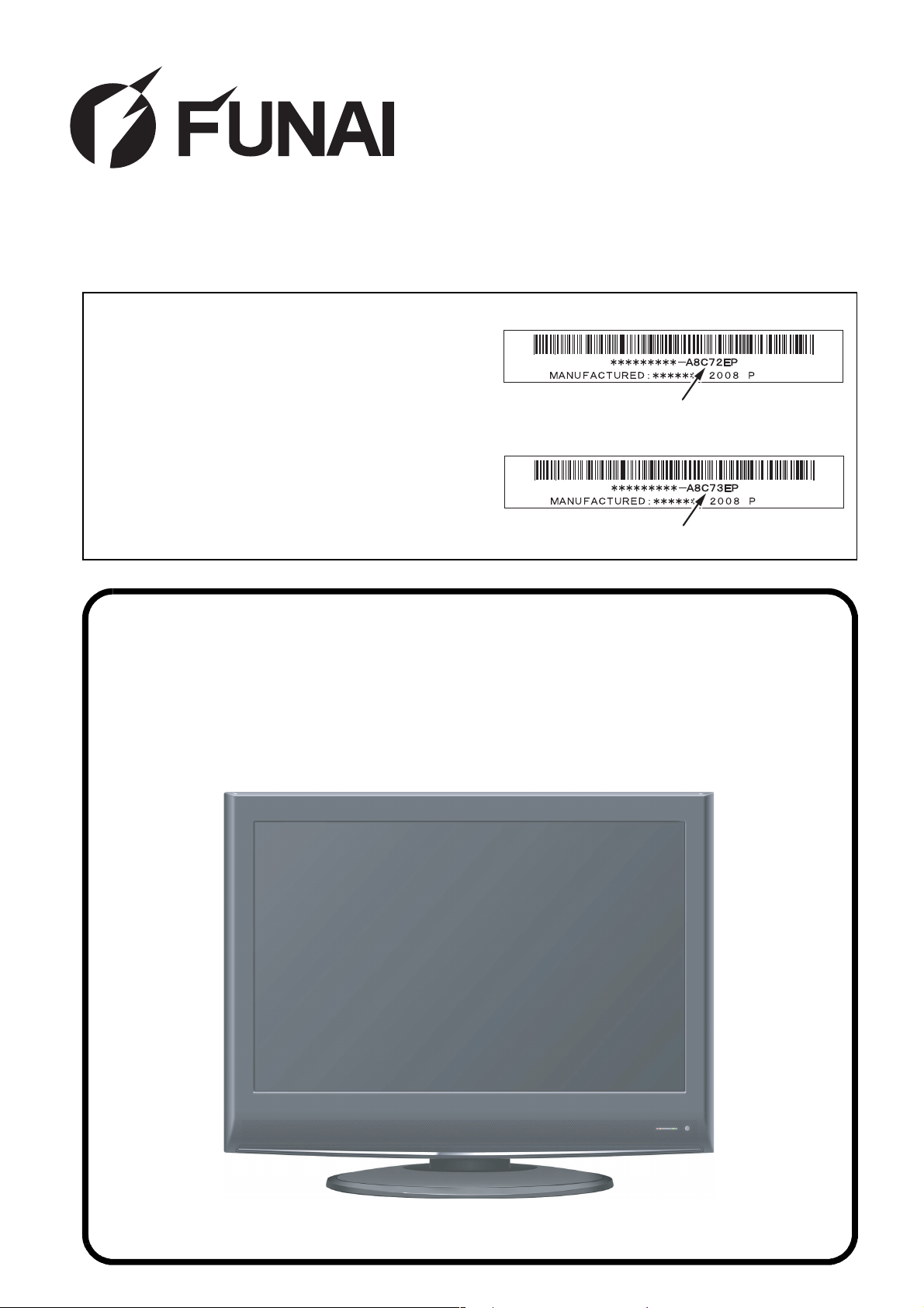
This Service Manual is for the
LT6-M22BB(A8C72EP)
/LT6-M22WB(A8C73EP) model.
For the LT6-M22BB(A8C72EP)
/LT6-M22WB(A8C73EP) model,
the letter (A8C72EP)/(A8C73EP) is
printed on the Serial No. Label.
Refer to the Serial No. Label on the
right.
Serial No. Label
"A8C72EP"
Serial No. Label
"A8C73EP"
22″ COLOR LCD TELEVISION
LT6-M22BB/LT6-M22WB
Page 2

22″ COLOR LCD TELEVISION
LT6-M22BB/LT6-M22WB
TABLE OF CONTENTS
Specifications . . . . . . . . . . . . . . . . . . . . . . . . . . . . . . . . . . . . . . . . . . . . . . . . . . . . . . . . . . . . . . . . . . . . . . . . . . . 1-1
Important Safety Precautions. . . . . . . . . . . . . . . . . . . . . . . . . . . . . . . . . . . . . . . . . . . . . . . . . . . . . . . . . . . . . . . 2-1
Standard Notes for Servicing . . . . . . . . . . . . . . . . . . . . . . . . . . . . . . . . . . . . . . . . . . . . . . . . . . . . . . . . . . . . . . . 3-1
Cabinet Disassembly Instructions . . . . . . . . . . . . . . . . . . . . . . . . . . . . . . . . . . . . . . . . . . . . . . . . . . . . . . . . . . . 4-1
Electrical Adjustment Instructions . . . . . . . . . . . . . . . . . . . . . . . . . . . . . . . . . . . . . . . . . . . . . . . . . . . . . . . . . . . 5-1
How to Initialize the LCD Television. . . . . . . . . . . . . . . . . . . . . . . . . . . . . . . . . . . . . . . . . . . . . . . . . . . . . . . . . . 6-1
Block Diagrams . . . . . . . . . . . . . . . . . . . . . . . . . . . . . . . . . . . . . . . . . . . . . . . . . . . . . . . . . . . . . . . . . . . . . . . . . 7-1
Schematic Diagrams / CBA and Test Points . . . . . . . . . . . . . . . . . . . . . . . . . . . . . . . . . . . . . . . . . . . . . . . . . . . 8-1
Waveforms . . . . . . . . . . . . . . . . . . . . . . . . . . . . . . . . . . . . . . . . . . . . . . . . . . . . . . . . . . . . . . . . . . . . . . . . . . . . . 9-1
Wiring Diagram . . . . . . . . . . . . . . . . . . . . . . . . . . . . . . . . . . . . . . . . . . . . . . . . . . . . . . . . . . . . . . . . . . . . . . . . 10-1
Exploded View . . . . . . . . . . . . . . . . . . . . . . . . . . . . . . . . . . . . . . . . . . . . . . . . . . . . . . . . . . . . . . . . . . . . . . . . . 11-1
Mechanical Parts List . . . . . . . . . . . . . . . . . . . . . . . . . . . . . . . . . . . . . . . . . . . . . . . . . . . . . . . . . . . . . . . . . . . . 12-1
Electrical Parts List. . . . . . . . . . . . . . . . . . . . . . . . . . . . . . . . . . . . . . . . . . . . . . . . . . . . . . . . . . . . . . . . . . . . . . 13-1
The LCD panel is manufactured to provide many years of useful life.
Occasionally a few non active pixels may appear as a tiny spec of color.
This is not to be considered a defect in the LCD screen.
Page 3
SPECIFICATIONS
< TUNER >
VHS/UHF Input ----------- 75Ω unbal., IEC Connector
Center IF ------------------- SECAM-L 38.9MHz, SECAM-L’ 33.9MHz
Description Condition Unit Nominal Limit
1. Video S/N 80 dB --- 40
2. Audio S/N --- dB --- 40/40
< LCD PANEL >
Description Condition Unit Nominal Limit
1. Number of Pixels
2. Viewing Angle
<DVB-T>
Description Condition Unit Nominal Limit
1. RECEIVED
FREQ.RANGE
(-60dBm, 45ch.) *1
2. INPUT DYNAMIC
RANGE (mix./max) *1
3. C/N PERFORMANCE
*1
4. MULTIPATH
a. Performance with
short delay echoes
b. Performance with
long delay echoes
c. C/N Performance on
0dB echo channel
(14µs)
Horizontal
Ver ti ca l
Horizontal
Ver ti ca l
+
-
VHF HIGH 7ch.
UHF 45ch.
VHF HIGH 7ch.
UHF 45ch.
UHF 45ch.
c:*2
d:*3
c:*2
d:*3
c:*1
pixels
pixels
kHz
kHz
dBm
dBm
dB
dB
dB
dB
dB
dB
dB
1680
1050
°
°
-85 to 85
-80 to 80
1000
900
-82.5/2
-81.1/2
15
15
18.7
14.0
19.1
13.0
20.7
---
---
---
---
500
-150
-75/-10
-75/-10
≦18
≦18
≦23
≦20
≦23
≦18
≦24
*1: modulation parameters = [8k 64QAM CR=2/3 GI=1/32]
*2: modulation parameters = [2k 64QAM CR=2/3 GI=1/32]
*3: modulation parameters = [2k 16QAM CR=3/4 GI=1/32]
< VIDEO >
Description Condition Unit Nominal Limit
1. Over Scan
2. Color Temperature
3. Resolution
4. Brightness AT 100% WHITE FIELD cd/m
Horizontal
Ver t i cal
AT 80% WHITE FIELD
x
y
Horizontal
Ver t i cal
line
line
%
%
°K 12000
2
5
5
0.272
0.278
400
350
250 ---
---
---
--±0.005
±0.005
---
---
1-1 A8C70SP
Page 4

< AUDIO >
All items are measured across 8 Ω load at speaker output terminal.
Description Condition Unit Nominal Limit
1. Audio Output Power 10% THD: Lch/Rch W 1.0/1.0 0.8/0.8
2. Audio Distortion 500mW: Lch/Rch % 1.5/1.5 3.0/3.0
-
3. Audio Freq. Response
6dB: Lch
-
6dB: Rch
Hz
Hz
70 to 8 k
70 to 8 k
---
---
4. Audio S/N
Note: Nominal specifications represent the design specifications. All units should be able to approximate these.
Some will exceed and some may drop slightly below these specifications. Limit specifications represent
the absolute worst condition that still might be considered acceptable. In no case should a unit fail to meet
limit specifications.
VIDEO
Component
dB
dB
---
---
>45/45
>45/45
1-2 A8C70SP
Page 5
IMPORTANT SAFETY PRECAUTIONS
Prior to shipment from the factory, our products are strictly inspected for recognized product safety and electrical
codes of the countries in which they are to be sold. However, in order to maintain such compliance, it is equally
important to implement the following precautions when a set is being serviced.
Safety Precautions for LCD TV
Circuit
1. Before returning an instrument to the
customer, always make a safety check of the
entire instrument, including, but not limited to, the
following items:
a. Be sure that no built-in protective devices are
defective and have been defeated during
servicing. (1) Protective shields are provided
on this chassis to protect both the technician
and the customer. Correctly replace all missing
protective shields, including any removed for
servicing convenience. (2) When reinstalling
the chassis and/or other assembly in the
cabinet, be sure to put back in place all
protective devices, including but not limited to,
nonmetallic control knobs, insulating
fishpapers, adjustment and compartment
covers/shields, and isolation resistor/capacitor
networks. Do not operate this instrument or
permit it to be operated without all
protective devices correctly installed and
functioning. Servicers who defeat safety
features or fail to perform safety checks
may be liable for any resulting damage.
b. Be sure that there are no cabinet openings
through which an adult or child might be able to
insert their fingers and contact a hazardous
voltage. Such openings include, but are not
limited to, (1) spacing between the LCD module
and the cabinet mask, (2) excessively wide
cabinet ventilation slots, and (3) an improperly
fitted and/or incorrectly secured cabinet back
cover.
c. Antenna Cold Check - With the instrument AC
plug removed from any AC source, connect an
electrical jumper across the two AC plug
prongs. Place the instrument AC switch in the
on position. Connect one lead of an ohmmeter
to the AC plug prongs tied together and touch
the other ohmmeter lead in turn to each tuner
antenna input exposed terminal screw and, if
applicable, to the coaxial connector. If the
measured resistance is less than 1.0 megohm
or greater than 5.2 megohm, an abnormality
exists that must be corrected before the
instrument is returned to the customer. Repeat
this test with the instrument AC switch in the off
position.
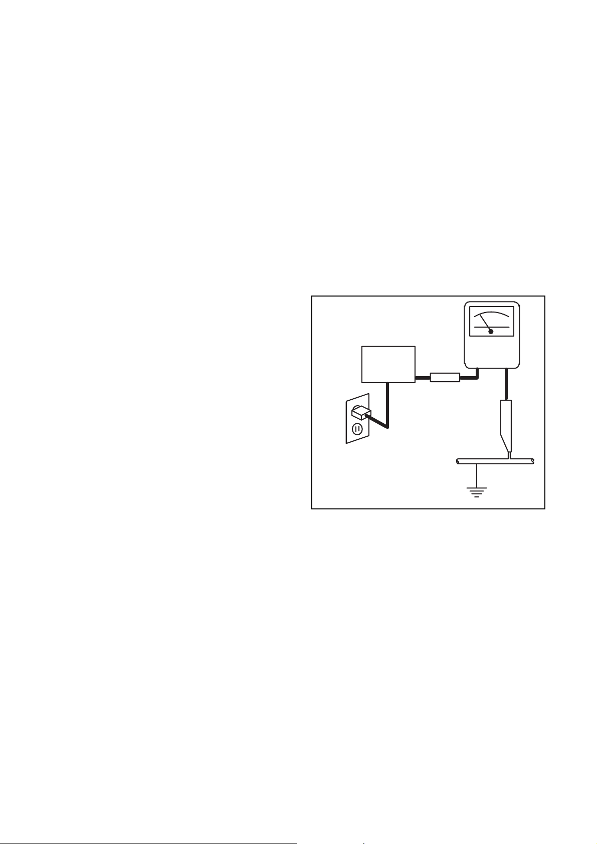
d. Leakage Current Hot Check - With the
instrument completely reassembled, plug the
AC line cord directly into a 230 V AC outlet. (Do
not use an isolation transformer during this
test.) Use a leakage current tester or a
metering system that complies with American
National Standards Institute (ANSI) C101.1
Leakage Current for Appliances and
Underwriters Laboratories (UL) 1410, (50.7).
With the instrument AC switch first in the on
position and then in the off position, measure
from a known earth ground (metal water pipe,
conduit, etc.) to all exposed metal parts of the
instrument (antennas, handle brackets, metal
cabinet, screw heads, metallic overlays, control
shafts, etc.), especially any exposed metal
parts that offer an electrical return path to the
chassis. Any current measured must not
exceed 0.5 milli-ampere. Reverse the
instrument power cord plug in the outlet and
repeat the test.
READING SHOULD
NOT BE ABOVE 0.5 mA
LEAKAGE
DEVICE
BEING
TESTED
TEST ALL EXPOSED
METAL SURFACES
ALSO TEST WITH
PLUG REVERSED
USING AC
ADAPTER PLUG
AS REQUIRED
ANY MEASUREMENTS NOT WITHIN THE
LIMITS SPECIFIED HEREIN INDICATE A
POTENTIAL SHOCK HAZARD THAT MUST
BE ELIMINATED BEFORE RETURNING THE
INSTRUMENT TO THE CUSTOMER OR
BEFORE CONNECTING THE ANTENNA OR
ACCESSORIES.
2. Read and comply with all caution and safety-
related notes on or inside the receiver cabinet, on
the receiver chassis, or on the LCD module.
3. Design Alteration Warning - Do not alter or add
to the mechanical or electrical design of this LCD
TV receiver. Design alterations and additions,
including, but not limited to circuit modifications
and the addition of items such as auxiliary audio
and/or video output connections, might alter the
safety characteristics of this receiver and create a
hazard to the user. Any design alterations or
additions will void the manufacturer's warranty and
may make you, the servicer, responsible for
personal injury or property damage resulting
therefrom.
CURRENT
TESTER
+
EARTH
GROUND
_
2-1 LTVP_ISP
Page 6

4. Hot Chassis Warning -
a. Some TV receiver chassis are electrically
connected directly to one conductor of the AC
power cord and maybe safety-serviced without
an isolation transformer only if the AC power
plug is inserted so that the chassis is
connected to the ground side of the AC power
source. To confirm that the AC power plug is
inserted correctly, with an AC voltmeter,
measure between the chassis and a known
earth ground. If a voltage reading in excess of
1.0 V is obtained, remove and reinsert the AC
power plug in the opposite polarity and again
measure the voltage potential between the
chassis and a known earth ground.
b. Some TV receiver chassis normally have 85V
AC(RMS) between chassis and earth ground
regardless of the AC plug polarity. This chassis
can be safety-serviced only with an isolation
transformer inserted in the power line between
the receiver and the AC power source, for both
personnel and test equipment protection.
c. Some TV receiver chassis have a secondary
ground system in addition to the main chassis
ground. This secondary ground system is not
isolated from the AC power line. The two
ground systems are electrically separated by
insulation material that must not be defeated or
altered.
5. Observe original lead dress. Take extra care to
assure correct lead dress in the following areas: a.
near sharp edges, b. near thermally hot parts-be
sure that leads and components do not touch
thermally hot parts, c. the AC supply, d. high
voltage, and, e. antenna wiring. Always inspect in
all areas for pinched, out of place, or frayed wiring.
Check AC power cord for damage.
6. Components, parts, and/or wiring that appear to
have overheated or are otherwise damaged
should be replaced with components, parts, or
wiring that meet original specifications.
Additionally, determine the cause of overheating
and/or damage and, if necessary, take corrective
action to remove any potential safety hazard.
7. Product Safety Notice - Some electrical and
mechanical parts have special safety-related
characteristics which are often not evident from
visual inspection, nor can the protection they give
necessarily be obtained by replacing them with
components rated for higher voltage, wattage, etc..
Parts that have special safety characteristics are
identified by a ! on schematics and in parts lists.
Use of a substitute replacement that does not
have the same safety characteristics as the
recommended replacement part might create
shock, fire, and/or other hazards. The product's
safety is under review continuously and new
instructions are issued whenever appropriate.
Prior to shipment from the factory, our products
are strictly inspected to confirm they comply with
the recognized product safety and electrical codes
of the countries in which they are to be sold.
However, in order to maintain such compliance, it
is equally important to implement the following
precautions when a set is being serviced.
2-2 LTVP_ISP
Page 7

Precautions during Servicing
A. Parts identified by the ! symbol are critical for
safety.
Replace only with part number specified.
B. In addition to safety, other parts and assemblies
are specified for conformance with regulations
applying to spurious radiation. These must also be
replaced only with specified replacements.
Examples: RF converters, RF cables, noise
blocking capacitors, and noise blocking filters, etc.
C. Use specified internal wiring. Note especially:
1) Wires covered with PVC tubing
2) Double insulated wires
3) High voltage leads
D. Use specified insulating materials for hazardous
live parts. Note especially:
1) Insulation Tape
2) PVC tubing
3) Spacers
4) Insulators for transistors.
E. When replacing AC primary side components
(transformers, power cord, etc.), wrap ends of
wires securely about the terminals before
soldering.
F. Observe that the wires do not contact heat
producing parts (heat sinks, oxide metal film
resistors, fusible resistors, etc.)
G. Check that replaced wires do not contact sharp
edged or pointed parts.
H. When a power cord has been replaced, check that
5~6 kg of force in any direction will not loosen it.
I. Also check areas surrounding repaired locations.
J. Use care that foreign objects (screws, solder
droplets, etc.) do not remain inside the set.
K. When connecting or disconnecting the internal
connectors, first, disconnect the AC plug from the
AC supply outlet.
L. When installing parts or assembling the cabinet
parts, be sure to use the proper screws and
tighten certainly.
2-3 LTVP_ISP
Page 8
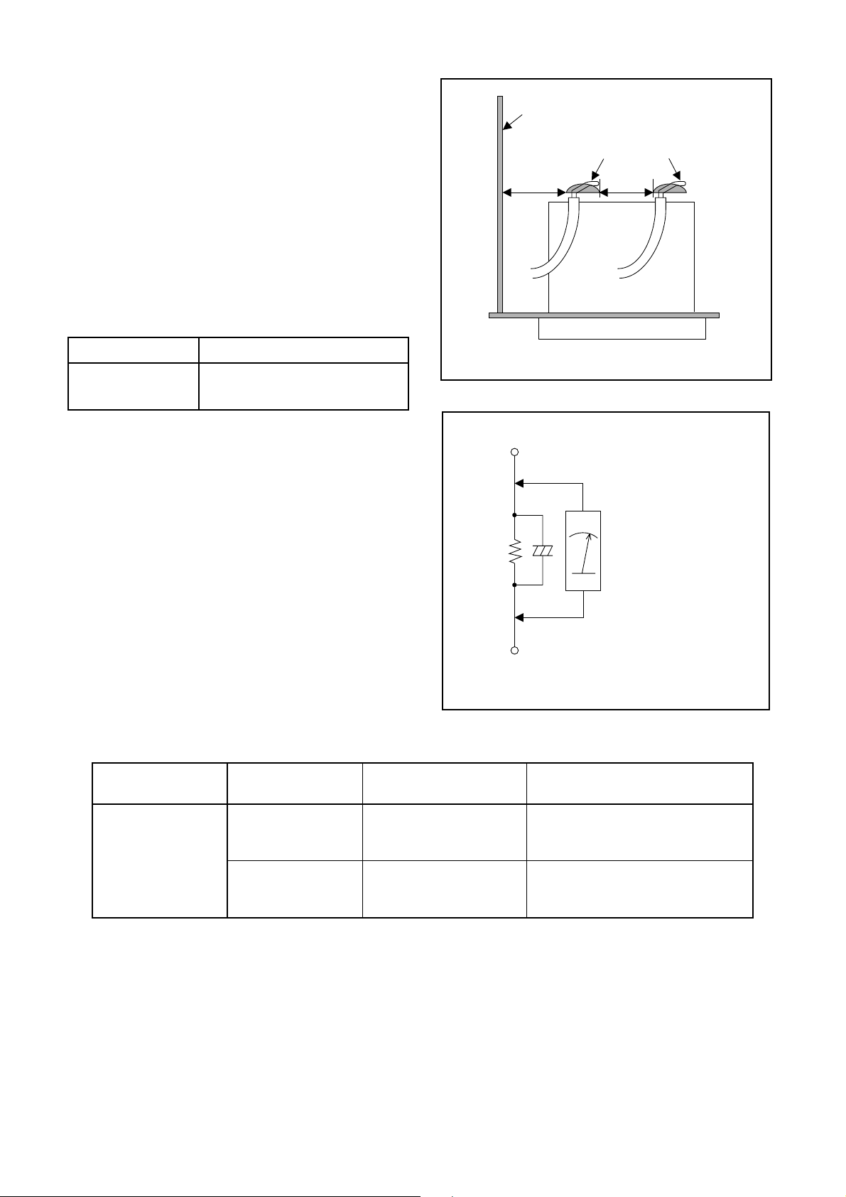
Safety Check after Servicing
Examine the area surrounding the repaired location
for damage or deterioration. Observe that screws,
parts and wires have been returned to original positions. Afterwards, perform the following tests and confirm the specified values in order to verify compliance
with safety standards.
1. Clearance Distance
When replacing primary circuit components, confirm
specified clearance distance (d) and (d') between soldered terminals, and between terminals and surrounding metallic parts. (See Fig. 1)
Table 1 : Ratings for selected area
AC Line Voltage Clearance Distance (d), (d’)
220 to 240 V
Note: This table is unofficial and for reference only.
Be sure to confirm the precise values.
≥ 3mm(d)
≥ 6 mm(d’)
2. Leakage Current Test
Confirm the specified (or lower) leakage current between B (earth ground, power cord plug prongs) and
externally exposed accessible parts (RF terminals, antenna terminals, video and audio input and output terminals, microphone jacks, earphone jacks, etc.).
Chassis or Secondary Conductor
Primary Circuit
d' d
Exposed Accessible Part
Z
AC Voltmeter
(High Impedance)
Fig. 1
Measuring Method : (Power ON)
Insert load Z between B (earth ground, power cord
plug prongs) and exposed accessible parts. Use an
AC voltmeter to measure across both terminals of load
Z. See Fig. 2 and following table.
Table 2: Leakage current ratings for selected areas
AC Line Voltage Load Z Leakage Current (i)
2kΩ RES.
Connected in
parallel
220 to 240 V
50kΩ RES.
Connected in
parallel
Note: This table is unofficial and for reference only. Be sure to confirm the precise values.
i≤0.7mA AC Peak
i≤2mA DC
i≤0.7mA AC Peak
i≤2mA DC
One side of
B
Power Cord Plug Prongs
One side of power cord plug
prongs (B) to:
Antenna terminals
A/V Input, Output
Fig. 2
RF or
2-4 LTVP_ISP
Page 9
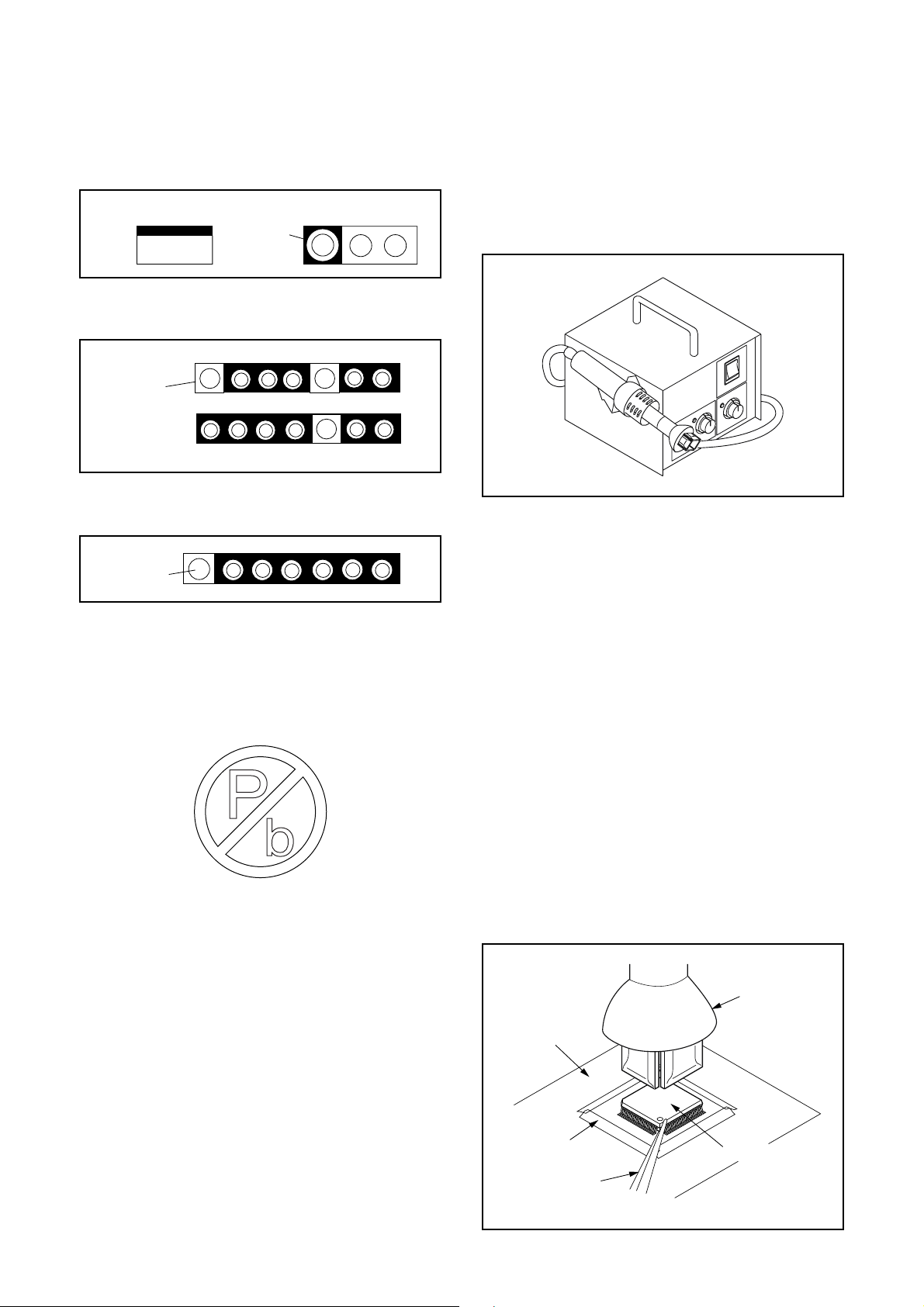
STANDARD NOTES FOR SERVICING
Circuit Board Indications
1. The output pin of the 3 pin Regulator ICs is
indicated as shown.
Top View
Out
2. For other ICs, pin 1 and every fifth pin are
indicated as shown.
Pin 1
3. The 1st pin of every male connector is indicated as
shown.
Pin 1
Input
In
Bottom View
5
10
Pb (Lead) Free Solder
Pb free mark will be found on PCBs which use Pb
free solder. (Refer to figure.) For PCBs with Pb free
mark, be sure to use Pb free solder. For PCBs
without Pb free mark, use standard solder.
Pb free mark
How to Remove / Install Flat Pack-IC
1. Removal
With Hot-Air Flat Pack-IC Desoldering Machine:
1. Prepare the hot-air flat pack-IC desoldering
machine, then apply hot air to the Flat Pack-IC
(about 5 to 6 seconds). (Fig. S-1-1)
Fig. S-1-1
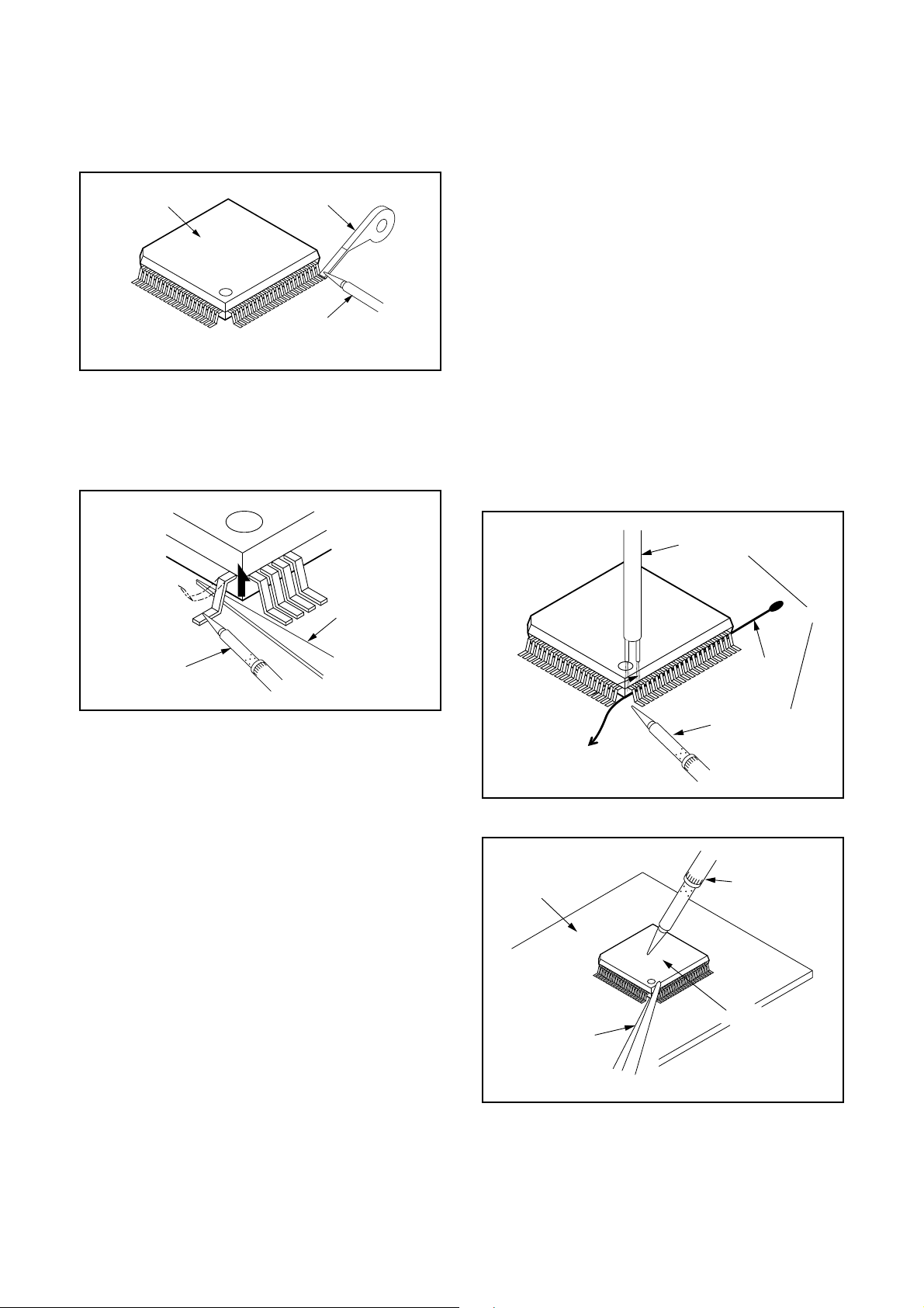
2. Remove the flat pack-IC with tweezers while
applying the hot air.
3. Bottom of the flat pack-IC is fixed with glue to the
CBA; when removing entire flat pack-IC, first apply
soldering iron to center of the flat pack-IC and heat
up. Then remove (glue will be melted). (Fig. S-1-6)
4. Release the flat pack-IC from the CBA using
tweezers. (Fig. S-1-6)
CAUTION:
1. The Flat Pack-IC shape may differ by models. Use
an appropriate hot-air flat pack-IC desoldering
machine, whose shape matches that of the Flat
Pack-IC.
2. Do not supply hot air to the chip parts around the
flat pack-IC for over 6 seconds because damage
to the chip parts may occur. Put masking tape
around the flat pack-IC to protect other parts from
damage. (Fig. S-1-2)
3. The flat pack-IC on the CBA is affixed with glue, so
be careful not to break or damage the foil of each
pin or the solder lands under the IC when
removing it.
Hot-air
Flat Pack-IC
Desoldering
CBA
Masking
Tape
Tweezers
3-1 TVP_SN
Machine
Flat Pack-IC
Fig. S-1-2
Page 10
With Soldering Iron:
1. Using desoldering braid, remove the solder from
all pins of the flat pack-IC. When you use solder
flux which is applied to all pins of the flat pack-IC,
you can remove it easily. (Fig. S-1-3)
Flat Pack-IC
Desoldering Braid
Soldering Iron
Fig. S-1-3
2. Lift each lead of the flat pack-IC upward one by
one, using a sharp pin or wire to which solder will
not adhere (iron wire). When heating the pins, use
a fine tip soldering iron or a hot air desoldering
machine. (Fig. S-1-4)
With Iron Wire:
1. Using desoldering braid, remove the solder from
all pins of the flat pack-IC. When you use solder
flux which is applied to all pins of the flat pack-IC,
you can remove it easily. (Fig. S-1-3)
2. Affix the wire to a workbench or solid mounting
point, as shown in Fig. S-1-5.
3. While heating the pins using a fine tip soldering
iron or hot air blower, pull up the wire as the solder
melts so as to lift the IC leads from the CBA
contact pads as shown in Fig. S-1-5.
4. Bottom of the flat pack-IC is fixed with glue to the
CBA; when removing entire flat pack-IC, first apply
soldering iron to center of the flat pack-IC and heat
up. Then remove (glue will be melted). (Fig. S-1-6)
5. Release the flat pack-IC from the CBA using
tweezers. (Fig. S-1-6)
Note: When using a soldering iron, care must be
taken to ensure that the flat pack-IC is not
being held by glue. When the flat pack-IC is
removed from the CBA, handle it gently
because it may be damaged if force is applied.
Sharp
Pin
Fine Tip
Soldering Iron
3. Bottom of the flat pack-IC is fixed with glue to the
CBA; when removing entire flat pack-IC, first apply
soldering iron to center of the flat pack-IC and heat
up. Then remove (glue will be melted). (Fig. S-1-6)
4. Release the flat pack-IC from the CBA using
tweezers. (Fig. S-1-6)
Fig. S-1-4
To Solid
Mounting Point
CBA
Hot Air Blower
or
Iron Wire
Soldering Iron
Fig. S-1-5
Fine Tip
Soldering Iron
Flat Pack-IC
Tweezers
Fig. S-1-6
3-2 TVP_SN
Page 11
2. Installation
1. Using desoldering braid, remove the solder from
the foil of each pin of the flat pack-IC on the CBA
so you can install a replacement flat pack-IC more
easily.
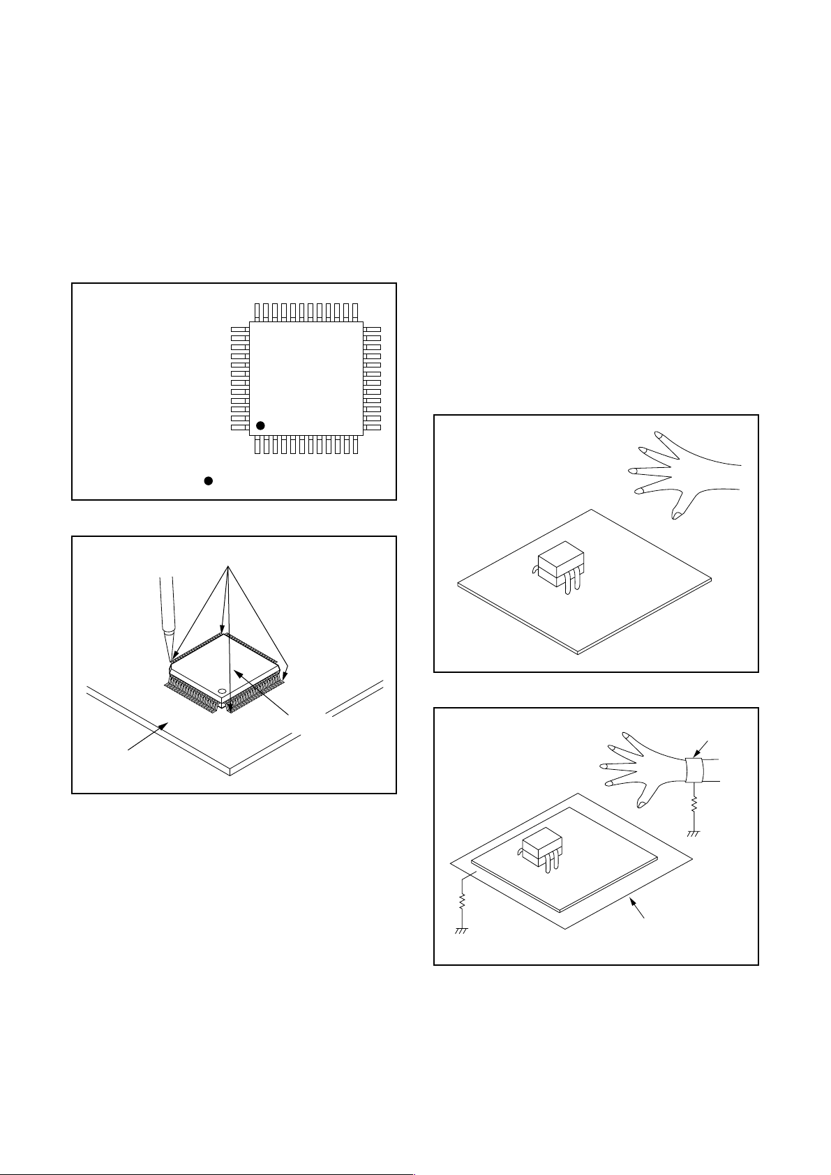
2. The “●” mark on the flat pack-IC indicates pin 1.
(See Fig. S-1-7.) Be sure this mark matches the 1
on the PCB when positioning for installation. Then
presolder the four corners of the flat pack-IC. (See
Fig. S-1-8.)
3. Solder all pins of the flat pack-IC. Be sure that
none of the pins have solder bridges.
Example :
Pin 1 of the Flat Pack-IC
is indicated by a " " mark.
Fig. S-1-7
Instructions for Handling Semiconductors
Electrostatic breakdown of the semi-conductors may
occur due to a potential difference caused by
electrostatic charge during unpacking or repair work.
1. Ground for Human Body
Be sure to wear a grounding band (1 MΩ) that is
properly grounded to remove any static electricity that
may be charged on the body.
2. Ground for Workbench
Be sure to place a conductive sheet or copper plate
with proper grounding (1 MΩ) on the workbench or
other surface, where the semi-conductors are to be
placed. Because the static electricity charge on
clothing will not escape through the body grounding
band, be careful to avoid contacting semi-conductors
with your clothing.
<Incorrect>
CBA
Presolder
Flat Pack-IC
Fig. S-1-8
<Correct>
1MΩ
CBA
Grounding Band
1MΩ
CBA
Conductive Sheet or
Copper Plate
3-3 TVP_SN
Page 12
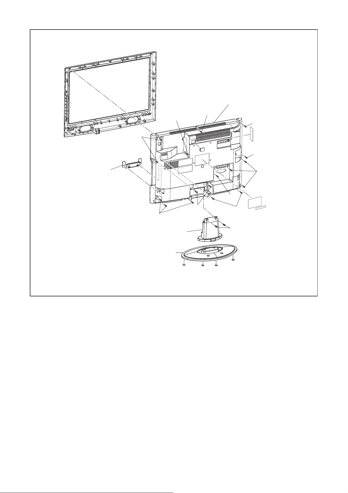
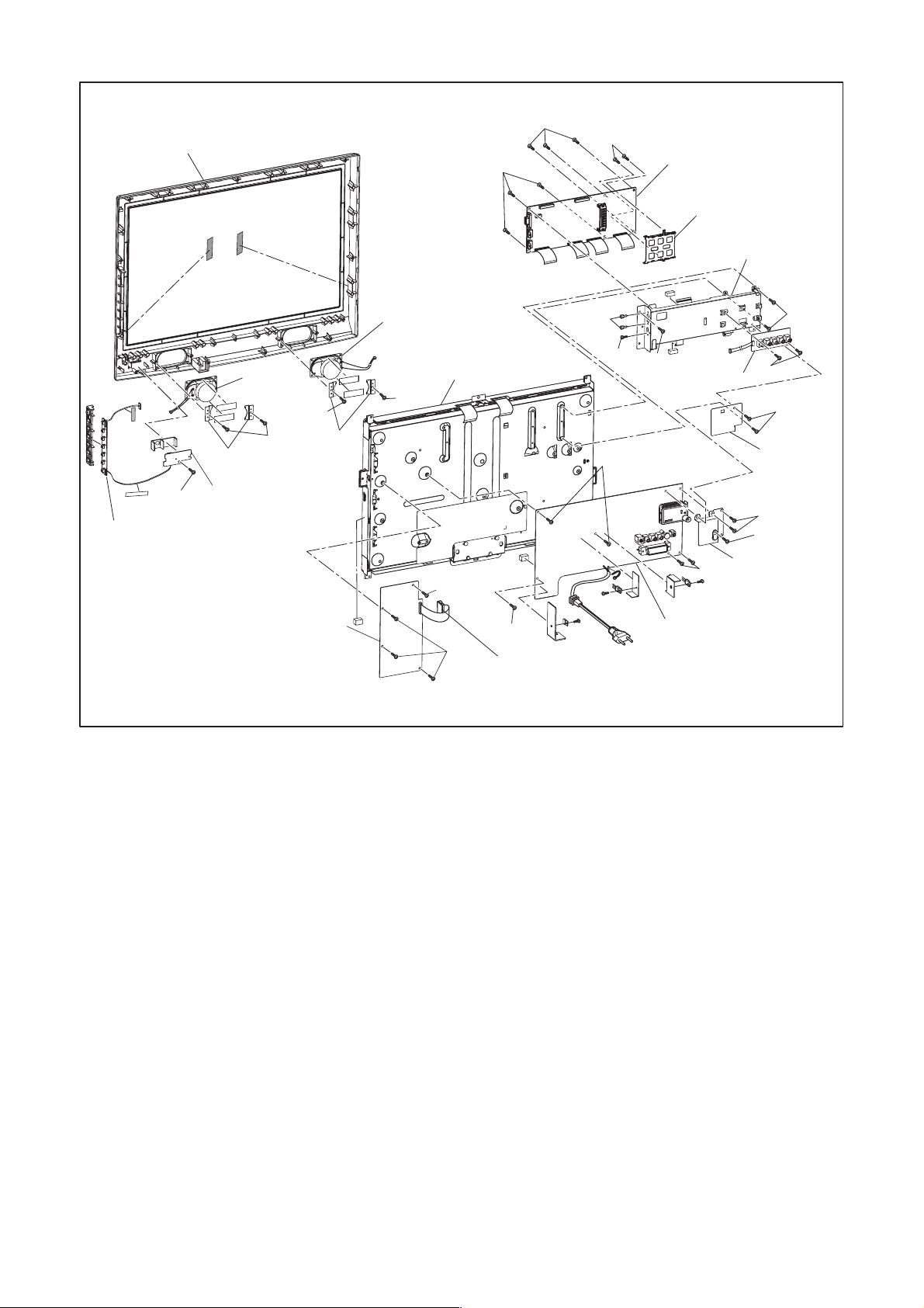
CABINET DISASSEMBLY INSTRUCTIONS
1. Disassembly Flowchart
This flowchart indicates the disassembly steps for the
cabinet parts, and the CBA in order to gain access to
item(s) to be serviced. When reassembling, follow the
steps in reverse order. Bend, route and dress the
cables as they were.
[16] Speaker(s)
[13] IR Sensor CBA
[14] Function CBA
[3] Rear Cabinet
[5] Jack CBA
[6] Shield Box
[7] Digital Main
CBA Unit
[8] FFC Shield
[9] Shield(T)
[10] Main CBA
[4] Stand Hinge
[1] Stand Cover
[2] Neck Cover
Removal
Step/
Loc.
No.
Part
Remove/*Unhook/
Fig.
No.
Unlock/Release/
Unplug/Unclamp/
Desolder
2(S-6), (S-7), 3(S-8),
6(S-9), *CN101A,
[6] Shield Box
D2
*CN102A, *CN103A,
D3
*CN104A, *CN4501,
*CN4502
Digital Main
[7]
CBA UnitD2D3
2(S-10), Connector IC
Card OSU
[8] FFC Shield D2 2(S-11) ---
[9] Shield(T) D2 2(S-12), (S-13) ---
4(S-14), (S-15),
D2
[10] Main CBA
Junction
[11]
CBA
Inverter
[12]
CBA
IR Sensor
[13]
CBA
*CN106, *CN105A,
D3
*CN802
D2
*CN404A ---
D3
4(S-16), *CN401,
D2
*CN402, *CN403,
D3
*CN451
D2
(S-17), *CN301 ---
D3
Note
---
---
---
---
[11] Junction CBA
[12] Inverter CBA
[15] LCD Module
Assembly
[17] Front Cabinet
2. Disassembly Method
Removal
Step/
Loc.
Part
No.
Stand
[1]
Cover
[2] Neck Cover D1 --------------- ---
Rear
[3]
Cabinet
Stand
[4]
Hinge
[5] Jack CBA
Remove/*Unhook/
Fig.
No.
Unlock/Release/
Unplug/Unclamp/
Desolder
D1 2(S-1) ---
D1 2(S-2), 3(S-3), 12(S-4) ---
D1 --------------- ---
D2
2(S-5), *CN107 ---
D3
Note
[14]
Function
CBA
D2
--------------- ---
D3
LCD
[15]
Module
D2 --------------- ---
Assembly
[16] Speaker(s) D2
Front
[17]
Cabinet
↓
(1)
↓
(2)
4(S-18),
Speaker Holder(s)
---
D2 --------------- ---
↓
(3)
↓
(4)
↓
(5)
Note:
(1) Order of steps in procedure. When reassembling,
follow the steps in reverse order. These numbers
are also used as the Identification (location) No. of
parts in figures.
(2) Parts to be removed or installed.
(3) Fig. No. showing procedure of part location
(4) Identification of parts to be removed, unhooked,
unlocked, released, unplugged, unclamped, or
desoldered.
P = Spring, L = Locking Tab, S = Screw,
CN = Connector
* = Unhook, Unlock, Release, Unplug, or Desolder
e.g. 2(S-2) = two Screws (S-2),
2(L-2) = two Locking Tabs (L-2)
(5) Refer to the following "Reference Notes in the
Ta b le . "
4-1 A8C72DC
Page 13
[3] Rear Cabinet
[4] Stand Hinge
(S-4)
(S-4)
[2] Neck Cover
[1] Stand Cover
(S-3)
(S-2)
(S-4)
(S-4)
(S-3)
(S-4)
(S-3)
(S-4)
(S-1)
Fig. D1
4-2 A8C72DC
Page 14
[17] Front Cabinet
(S-9)
(S-9)
(S-10)
[7] Digital Main
CBA Unit
Connector IC
Card OSU
[6] Shield Box
Speaker
Holders
(S-17)
[13] IR Sensor
CBA
[14] Function CBA
[12] Inverter CBA
[16]
Speaker
(S-18)
(S-18)
Speaker
Holders
[16] Speaker
[15] LCD Module
Assembly
(S-18)
(S-16)
(S-16)
(S-6)
(S-7)
(S-14)
(S-15)
[11] Junction CBA
(S-8)
[5] Jack CBA
(S-14)
[10] Main CBA
(S-8)
(S-5)
(S-11)
[8] FFC
Shield
(S-12)
(S-13)
[9] Shield(T)
Fig. D2
4-3 A8C72DC
Page 15
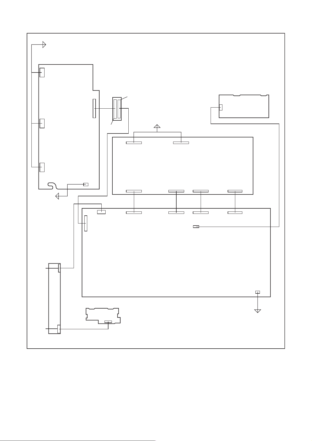
TV Cable Wiring Diagram
To LCD Module
Assembly
Inverter CBA
CN401
CN402
CN403
To Speaker
CN404B
CN451
CN106
CN105A
Junction
CBA
CN404A
Jack CBA
CL404
CN11
To LCD Module
Assembly
Digital Main CBA Unit
CN4501 CN4502
CN3704CN4503CN3701CN3601
Main CBA
CN103ACN102ACN101ACN104A
CN107
CN201
CN202
Function
CBA
IR Sensor CBA
CN301
CN802
To Speaker
Fig. D3
4-4 A8C72DC
Page 16
ELECTRICAL ADJUSTMENT INSTRUCTIONS
General Note: “CBA” is abbreviation for
“Circuit Board Assembly.”
Note: Electrical adjustments are required after
replacing circuit components and certain
mechanical parts. It is important to perform
these adjustments only after all repairs and
replacements have been completed.
Also, do not attempt these adjustments unless
the proper equipment is available.
Test Equipment Required
1. DC Voltmeter
2. Pattern Generato
3. Color Analyzer
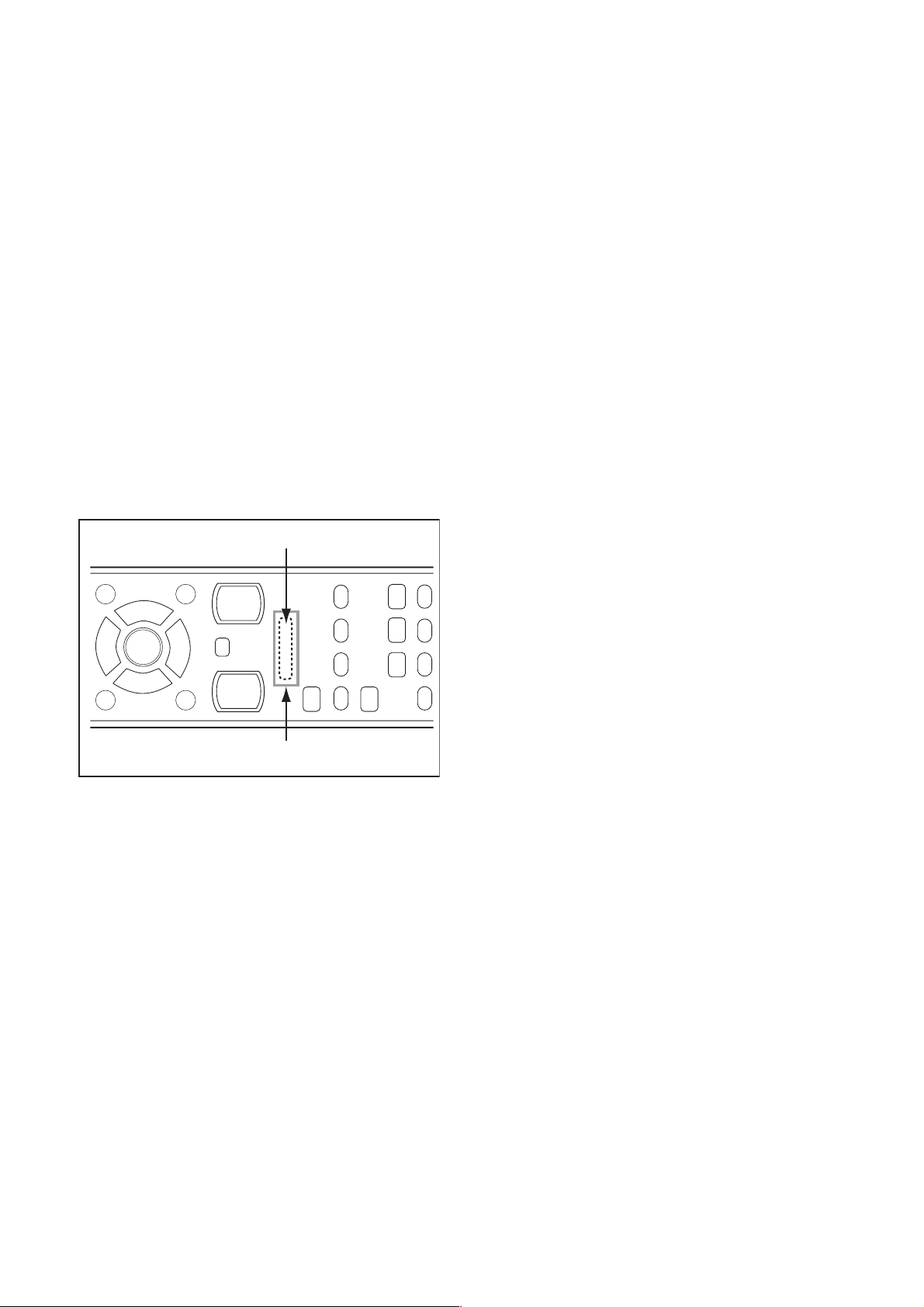
How to make the Service remote
control unit:
Cut “A” portion of the attached remote control unit as
shown in Fig. 1.
service button
How to set up the service mode:
Service mode:
1. Use the service remote control unit.
2. Turn the power on.
3. Press the service button on the service remote
control unit as shown in Fig.1.
A
Fig. 1
5-1 A8C70EA
Page 17
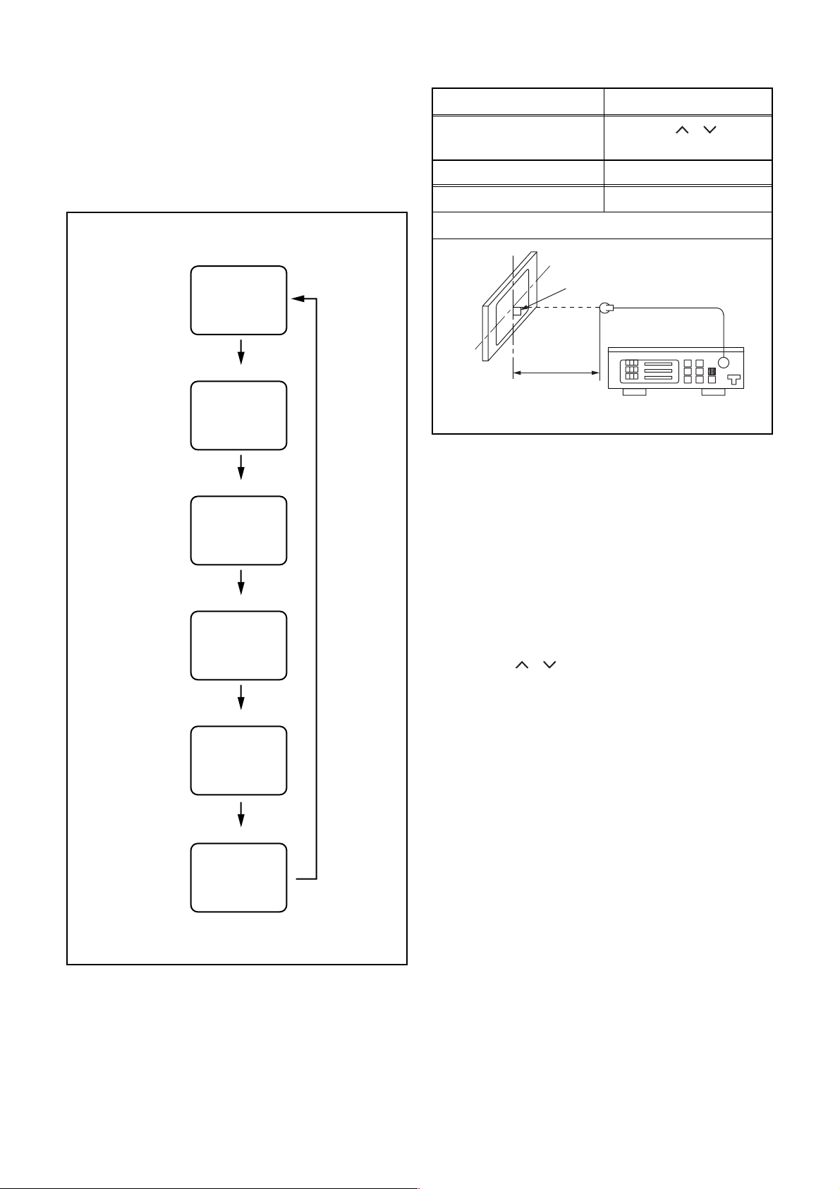
1. Purity Check Mode
2. VCOM Adjustment.
This mode cycles through full-screen displays of red,
green, blue, and white to check for non-active pixels.
1. Enter the Service mode.
2. Each time pressing [7] button on the service
remote control unit, the display changes as
follows.
Purity Check Mode
White mode
[7] button
[7] button
Black mode
[7] button
Red mode
[7] button
Green mode
[7] button
Blue mode
Test Point
Screen
Adj. Point
[P / ]
buttons
M. EQ. Spec.
Color analyzer
See below
Figure
It carries out in a darkroom.
Perpendicularity
L = 3 cm
Color Analyzer
1. Operate the unit for more than 20 minutes.
2. Set the color analyzer and bring the optical
receptor to the center on the LCD-Panel surface
after zero point calibration as shown above.
Note: The optical receptor must be set
perpendicularly to the LCD Panel surface.
3. Enter the Service mode.
4. [VCOM1]
Press [2] button on the service remote control unit.
[VCOM2]
Press [3] button on the service remote control unit.
5. Press [P / ] buttons on the service remote
control unit so that the color analyzer value
becomes minimum.
[7] button
White 25% mode
Note:
When entering this mode, the default setting is White mode.
5-2 A8C70EA
Page 18
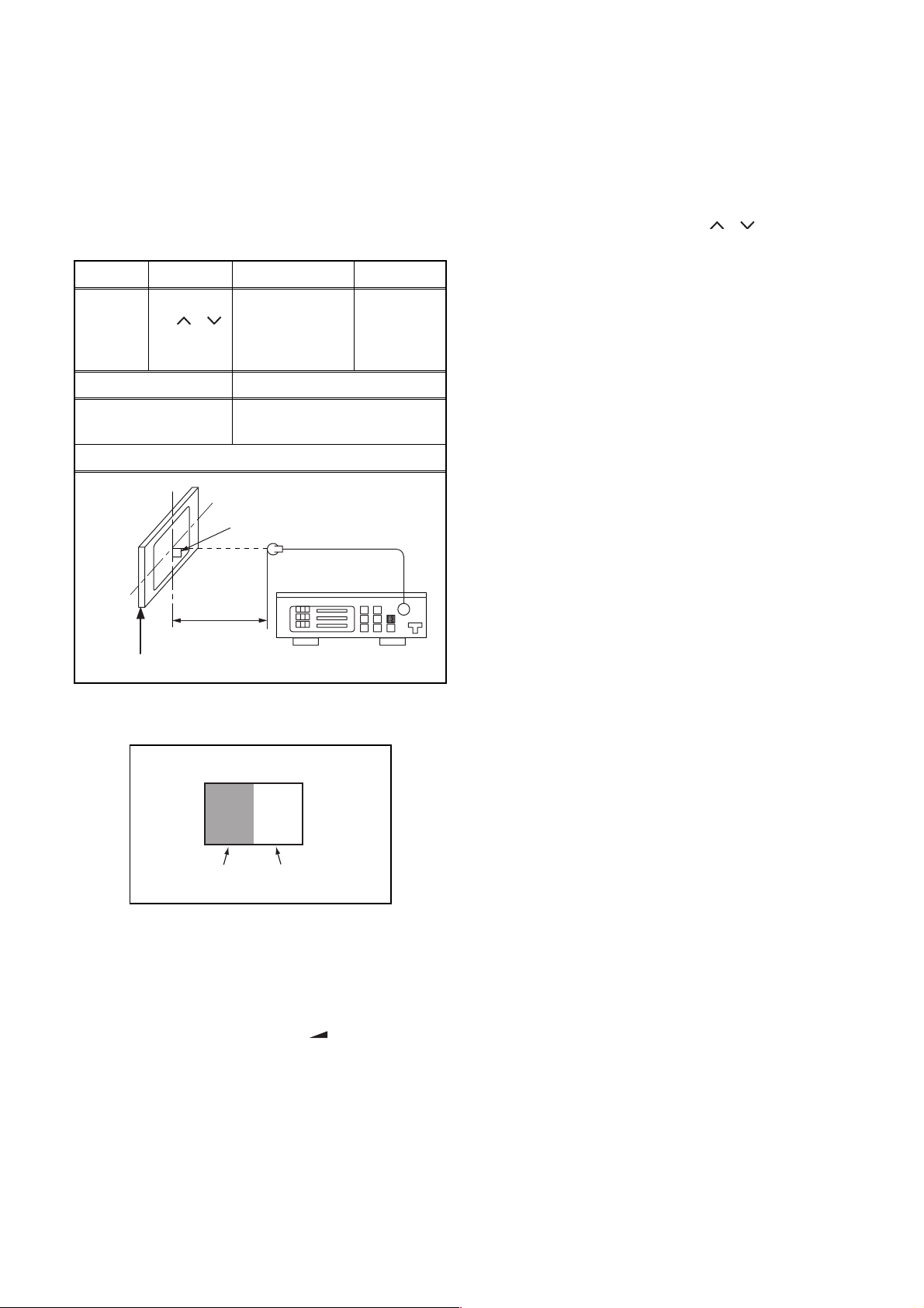
The following adjustment normally are not attempted in
the field. Only when replacing the LCD Panel then adjust
as a preparation.
3. White Balance Adjustment
Purpose: To mix red, green and blue beams correctly
for pure white.
Symptom of Misadjustment: White becomes bluish
or reddish.
Tes t Po i nt
Screen
Adj. Point Mode Input
[P / ]
buttons
[VIDEO]
C/D
M. EQ. Spec.
White Raster
(APL 70%)
or
(APL 25%)
5. [CUTOFF]
Press [3] button to select “COB” for Blue Cutoff
adjustment. Press [1] button to select “COR” for
Red Cutoff adjustment.
[DRIVE]
Press [6] button to select “DB” for Blue Drive
adjustment. Press [4] button to select “DR” for Red
Drive adjustment.
6. In each color mode, press [P / ] buttons to
adjust the values of color.
7. Adjust Cutoff and Drive so that the color
temperature becomes 12000°K (x
=
0.272 / y
=
0.278 ±0.005).
Pattern Generator,
Color analyzer
x= 0.272 ± 0.005
y= 0.278 ± 0.005
Figure
It carries out in a darkroom.
Perpendicularity
L = 3 cm
INPUT: WHITE 70%, 30%
Color Analyzer
1. Operate the unit for more than 20 minutes.
2. Input the White Raster(70%=70IRE, 30%=30IRE).
INPUT SIGNAL
30%=30IRE
70%=70IRE
3. Set the color analyzer to the CHROMA mode and
bring the optical receptor to the center on the
LCD-Panel surface after zero point calibration as
shown above.
Note: The optical receptor must be set
perpendicularly to the LCD Panel surface.
4. Enter the Service mode. Press [ -] button on the
service remote control unit and select “C/D” mode.
5-3 A8C70EA
Page 19

HOW TO INITIALIZE THE LCD TELEVISION
How to initialize the LCD television:
1. Turn the power on.
2. To enter the service mode, press the service
button on the service remote control unit. (Refer to
page 5-1.)
- To cancel the service mode, Press [ ] button on
the remote control unit.
3. Press [ ] button on the service remote control
unit to initialize the LCD television.
4. "INITIALIZED" will appear in the upper right of the
screen. "INITIALIZED" color will change to green
from red when initializing is complete.
6-1 A8CN0INT
Page 20
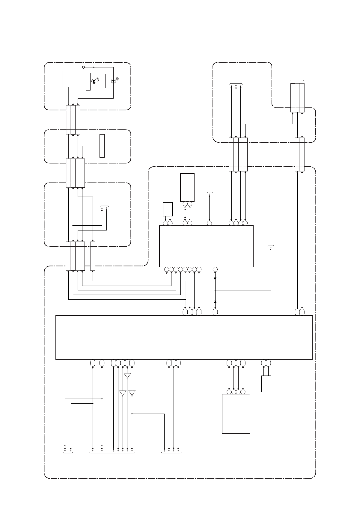
BLOCK DIAGRAMS
System Control Block Diagram
+3.3V
SENSOR
REMOTE
RS301
CN301
D303
LED144
REMOTE22
P-ON-H155
STANDBY
D302
POWER
IR SENSOR CBAFUNCTION CBAMAIN CBA
TO
INVERTER
BLOCK
DIAGRAM
PROTECT3
101211
CN105A
BACKLIGHT-SW
(CL404)
BACKLIGHT-ADJ
TO POWER
SUPPLY
BLOCK
DIAGRAM
RESET
PROTECT1
PROTECT2
MAIN CBA
CN202
KEY SWITCH
CN201
LED144
REMOTE22
P-ON-H155
KEY-IN166
CN106
TO POWER
P-ON-H1
CN104ACN3601
REMOTE22 4
CN101A
P-ON-H1125
P-ON-H213 13
KEY-IN125 1
CN3701
LED118 8
SUPPLY
BLOCK
DIAGRAM
P-ON-H2
(SUB MICRO CONTROLLER)
IC4700
X3101
4MHz
OSC
6
XOUT
LED1
12
8
XIN
KEY-IN1
24
IC3102 (MEMORY)
P-ON-H1
P-ON-H2
14
13
SDA
5
20
SDA
REMOTE
11
R22
REMOTE
SCL
6
19
SCL
RXD
15
P22
TXD1
TXD
16
N22
RXD1
RESET-MAIN
5
V24
RESET-MAIN
TO DIGITAL
SIGNAL
PROCESS
BLOCK
DIAGRAM
VCOM-PWM
21
VCOM-PWM
AMP-MUTE-SUB
18
AA2
AMP-MUTE-MAIN
CN101ACN3701
PROTECT121 5
22
PROTECT1
PROTECT220 6
RESET17 9
3
23
RESET
PROTECT2
PROTECT319 7
4
PROTECT3
TO AUDIO-2
BLOCK
DIAGRAM
AMP-MUTE
3
CN104ACN3601
BACKLIGHT-SW
A2
BACKLIGHT-SW
BACKLIGHT-ADJ
24223
AC24
BACKLIGHT-ADJ
IC4513
(MAIN MICRO CONTROLLER)
SDA
TO VIDEO
SCL
BLOCK
DIAGRAM
SCL
SCL
AF12
SDA
AE12
SDA
INPUT0
NICAM-RESET
SCART-MUTE
B2
A11
B11
Q3819
Q3823
INPUT0
NICAM-RESET
SCART-MUTE
INPUT1
TO AUDIO-1
BLOCK
DIAGRAM
INPUT2
INPUT1
E12
D12
Q3822
INPUT2
INPUT2
SLOW-SW1
TO VIDEO
SLOW-SW1E1FBIN1
D1
S-SW
FBIN1
BLOCK
DIAGRAM
7-1
S-SW
C12
CLKOUT
U25
25MHz
X3301
CLKIN
U26
OSC
DIGITAL MAIN CBA UNIT
SPI-CLK
SPI-DO
SPI-DI
SPI-CS
Y25
Y24
W25
W24
652
1
SI
CS
SO
SCK
IC3706 (MEMORY)
A8C72BLS
Page 21

Video Block Diagram
TO DIGITAL
SIGNAL
PROCESS
BLOCK
DIAGRAM
TO SYSTEM
CONTROL
BLOCK
DIAGRAM
TO DIGITAL
SIGNAL
PROCESS
BLOCK
DIAGRAM
TO SYSTEM
CONTROL
BLOCK
DIAGRAM
TO DIGITAL
SIGNAL
PROCESS
BLOCK
DIAGRAM
AUDIO SIGNAL
TS-DATA
VIDEO SIGNAL
IC3824 (DEMODULATOR)
58
DIF-OUT120 4
CN103A CN3704
SCL
13
MPEG2-TS
INTERFACES
DEMODULATOR
57
IF-AGC18 6
DIF-OUT222 2
25
SCL
SCL
64
SCL15 9
SDA
26
SDA
SDA2IF-AGC
63
SDA16 8
TU-CVBS11 13
VIDEO
CN102A CN4503
WF7WF6WF5
VIDEO-B
VIDEO-R
VIDEO-G
TU-CVBS
DTV-CVBS
VIDEO-R323
VIDEO-B521
VIDEO-G422
VIDEO125
TU-VIDEO13 13
SLOW-SW123 3
5
3
IC3823
(INPUT SELECT)
4
FBIN122 4
WF4
SW CTL
109 11
INPUT2
SLOW-SW1
FBIN1
S-SW
CN3704
S-SW123
INPUT2618
CN103A
WF3WF2
S-VIDEO-Y
S-VIDEO-C
S-VIDEO-Y23 3
S-VIDEO-C25 1
CN101A CN3701
COMP-Y
COMP-Pb
COMP-Pb20 6
COMP-Y18 8
COMP-Pr
COMP-Pr21 5
15
DIF-OUT1
TU501
(TUNER UNIT)
8
16
17
SCL
IF-AGC
DIF-OUT2
BUFFER
Q505
6
9SDA
VIDEO-OUT
15
IC851
(INPUT SELECT)
2
JK722
VIDEO-IN
1
SW CTL
MAIN CBA DIGITAL MAIN CBA UNIT
109 11
CN107CN11
COMP-Y11
COMP-Pb22
COMP-Pr44
JACK CBA
JK11
JK12
JK13
COMPONENT
-Y-IN
COMPONENT
-Pb-IN
COMPONENT
-Pr-IN
JK751
15
20VIDEO-IN
VIDEO-R
7
11
VIDEO-B
VIDEO-G
BUFFER BUFFER
Q726 Q744
19
VIDEO-OUT
Q734
8
SLOW-SW
Q731
16
RAPID-SW
CY
JK721
S-VIDEO-IN
7-2
A8C72BLV
Page 22

Audio-1 Block Diagram
TO
DIGITAL
SIGNAL
PROCESS
BLOCK
DIAGRAM
AUDIO SIGNAL
ACLK
BCLK
LRCLK
AD ATA 1
AUX-ADATA
TO SYSTEM
CONTROL
INPUT0
INPUT1
BLOCK
DIAGRAM
INPUT2
BUFFER
Q3831
BUFFER
Q3832
TO SYSTEM
CONTROL
BLOCK
DIAGRAM
SCART-MUTE
IC3825
(AUDIO A/D CONVERTER)
111015
12
A/D
CONVERTER
(L-CH)
(R-CH)
1
2
CN3704CN103A
AUDIO(L)321
AUDIO(R)420
INPUT0816
IC3822
(AUDIO D/A CONVERTER)
INPUT2618
INPUT1717
IC850
(INPUT SELECT)
124
3
8
(L-CH)
15
5
7
D/A
6
CONVERTER
(R-CH)
14
(L-CH)
5
IC3823
CN4503CN102A
TU-AUDIO(L)10 16
TU-AUDIO(R)11 15
13
Q3833
15
(INPUT SELECT)
1
2
Q3834
14
I2C BUS
I/F
RESET
19
18
21
SCL
NICAM-RESET
DIGITAL MAIN CBA UNIT
109 11
SW CTL
13
12
24
22
(L-CH)
(R-CH)
AUDIO SIGNAL
PROCESS
IC3821 (SOUND PROCESSOR)
3
SDA
MAIN CBA
9 10
SW CTL
(R-CH)
12
11
15
14
CN3704CN103A
TO SYSTEM
CONTROL
BLOCK
DIAGRAM
CN107CN11
COMP-AUDIO(L)
COMP-AUDIO(R)
66
77
JK15
JK14
COMPONENT
AUDIO(L)-IN
JACK CBA
COMPONENT
AUDIO(R)-IN
4
IC851
(INPUT SELECT)
5
JK723
AUDIO(L)-IN
3
(L-CH)
JK724
14
(R-CH)
12
13
AUDIO(R)-IN
SW CTL
7-3
SIF915
109 11
4
JK751
2
6AUDIO(L)-IN
AUDIO(R)-IN
3
1
AUDIO(L)-OUT
AUDIO(R)-OUT
JK725
PC-AUDIO
-IN
SIF-OUT
TU501
(TUNER UNIT)
A8C72BLA1
Page 23

Audio-2 Block Diagram
SP802
SPEAKER
L-CH
2
JK801
HEADPHONE
JACK
CL451
SP451
SPEAKER
R-CH
2
AUDIO SIGNAL
SP(L) 1
CN802 CL802
IC801 (AUDIO AMP)
SP-GND
11
AMP
(L-CH)
6
VOLUME
MUTE
/STANDBY
SP(R) 1
CN451
SP-GND
INVERTER CBA
CN404B
WF1
14
AMP
7
2
CONTROL
(R-CH)
1
+9V
SP(R)13 13SP(R)13 13
CN404ACN105A
CL404
JUNCTION
CBA
IC802
(AUDIO D/A CONVERTER)
(L-CH)
8
CN101ACN3701
LRCLK11 15
LRCLK
TO
DIGITAL
15
D/A
CONVERTER
BCLK12 14
BCLK
AD ATA
SIGNAL
PROCESS
(R-CH)
AD ATA13 13
14
567
ACLK14 12
AMP-MUTE917
ACLK
BLOCK
DIAGRAM
AMP-MUTE
TO SYSTEM
CONTROL
BLOCK
DIAGRAM
AMP MUTE
Q805
SWITCHING
Q802
MAIN CBA
DIGITAL MAIN CBA UNIT
7-4
A8C72BLA2
Page 24

Digital Signal Process Block Diagram
LCD MODULE
ASSEMBLY
BRSB2(+)52
CN4501
AUDIO SIGNAL
757473727170666564
VIDEO SIGNAL
IC4201(LCD DRIVE)
BRSB2(-)51
BRSB1(+)50
BRSB1(-)49
BRSB0(+)48
BRSB0(-)47
BRSG2(+)46
BRSG2(-)45
BRSG1(+)44
BRSG1(-)43
BRSG0(+)42
BRSG0(-)41
BRSR2(+)17
63
62616059585756556968777881
D-RSDS
OUTPUT
LVDS
RX
242522232021161718
AF20
AE20
AD19
AD20
AE19
AF19
AF18
AE18
BRSR2(-)16
AE21
BRSR1(+)15
19
AF21
BRSR1(-)14
BRSR0(+)13
BRSR0(-)12
BRSCLK(+)22
VCOM7
BRSCLK(-)21
TP119
POL18
STV5
LVDS
FRSB2(+)53
FRSB2(-)52
FRSB1(+)51
FRSB1(-)50
FRSB0(+)49
FRSB0(-)48
FRSG2(+)47
FRSG2(-)46
FRSG1(+)45
VCOM9
CN4502
52515049484744434140393837363534333246
DATA
MAPPING
TX
FRSG1(-)44
D-RSDS
LVDS
9107856123
AF25
AF24
AE25
AD25
AD26
FRSG0(+)43
FRSG0(-)42
OUTPUT
RX
AE24
AD23
FRSR2(+)18
AD24
FRSR2(-)17
AF26
FRSR1(+)16
4
AE26
FRSR1(-)15
FRSR0(+)14
FRSR0(-)13
FRSCLK(+)23
FRSCLK(-)22
STH-F55
CPV6
OE15
STV7
TP120
POL19
DRIVE
IC4511,Q4511,
145
808284
IC4202 (MEMORY)
SCL
87
6
SCL
(SDRAM)
IC3201
SDA
88
5
SDA
Q4512,Q4513
TO SYSTEM
DATA(0-15)
H1,H3,H7,H9
B1,B9,C2,C8,
F1,F9,G2,G8,
M2,M3,M7,M8,
D1,D3,D7,D9,
A13-15,A18,
A21-23,B13-15,
B17,B19-23
C15,C17-19,
VCOM-PWM
CONTROL
BLOCK
DIAGRAM
ADDESS(0-12)
N2,N3,N7,N8,
P2,P3,P7,P8,R2
C23,C24,D14,
D15,D17-19,
D22,D23
IC4513 (DIGITAL SIGNAL PROCESS)
DIGITAL MAIN CBA UNIT
T4
Y3
COMP-Y
TU-CVBS
T3
U4
COMP-Pr
COMP-Pb
U3
W3
VIDEO
S-VIDEO-Y
TO VIDEO
BLOCK
DIAGRAM
A/D
CONVERTER
SW
V3V4Y2
S-VIDEO-C
VIDEO-R
Y1
AA1
VIDEO-G
VIDEO-B
JK3701
T5
1
RED
R4R3R5
3
2
BLUE
GREEN
VGA-HSYNC
K5
14
13
VSYNC
HSYNC
D-SUB
VGA-VSYNC
L5
SDA
IC3701 (MEMORY)
5
12
15
DATA
CLOCK
AB25
SCL
6
TS I/F
AB12
TS-DATA
DTV-CVBS
TO VIDEO
BLOCK
DIAGRAM
DIGITAL
SIGNAL
PROCESS
AUDIO I/F
AF15
AE15
AE16
AC17
AD15
AUX-ADATA
BCLK
AD ATA 1
TO AUDIO-1
LRCLK
BLOCK
DIAGRAM
ACLK
AD ATA
AD16
BCLK
LRCLK
TO AUDIO-2
BLOCK
ACLK
DIAGRAM
TMDS-D0(+)
JK4001
AUDIO
DECODER
A9
B9
C8
C9
TMDS-D0(-)
TMDS-D1(+)
TMDS-D1(-)
79461
HDMI
I/F
B8
A8
B10
TMDS-CLOCK(+)
TMDS-CLOCK(-)
TMDS-D2(+)
TMDS-D2(-)
3
101216
HDMI-IN1
VIDEO
DECODER
E9
A10
Q4002
BUFFER
SDA
SCL
C10
Q4001
BUFFER
15
Y22,Y23,AA21-23,
AB21-23,AF7-11,
AE9,AE10,AD10
D(0-7)
3,4,7,8,
13,14,
(LATCH)
LATCH
IC3826
2,5,6,
D(0-15)
9,12,15
A(8-13)
CI
CARD
17,18
SLOT
V21,W21,Y21,
AA20,AC20,AC21
AE14,AF14
A(0-7)
A(0-13)
7-5
A8C72BLD
Page 25

Inverter Block Diagram
BACK
LIGHT
1
2
CN401
786
5
BACK
1
CN402
LIGHT
2
786
BACK
LIGHT
LCD MODULE
ASSEMBLY
1
2
CN403
5
786
5
T401
Q405
SW+16V
Q401,Q415Q417,Q429
3
2
CURRENT
CONTROL
SWITCH
IC401
(PWM CONTROL)
1
VCC
12
T402
Q416
Q410,
Q413
Q412
15
3
2
CURRENT
CONTROL
DRIVE
SWITCHING
8
PWM
CONTROL
16
1
SWITCH
Q404,
Q406
Q407
LOGIC
2
4
3
4
DRIVE
SWITCHING
11
1
T403
OSC
Q424
2
3
CURRENT
CONTROL
5 6
1
SWITCH
Q421
Q420
4
Q422
OVER VOLTAGE
PROTECTOR
OVER VOLTAGE
PROTECTOR
OVER VOLTAGE
PROTECTOR
OVER VOLTAGE
PROTECTOR
OVER VOLTAGE
PROTECTOR
OVER VOLTAGE
Q427
Q414
Q419
Q403
Q409
PROTECTOR
INVERTER CBA
Q428
F401
3.15A
CN404B
CL404 CN404A
TO POWER
SUPPLY
2,5,6
INV+22V
2,5,6
2,5,6
INV+22V
BLOCK
DIAGRAM
(CN105A)
SW+22V
Q423,
Q425
SW
CN404B
12
11
10
BACKLIGHT-ADJ
BACKLIGHT-SW
PROTECT3
12
11
10
JUNCTION
CBA
A8C72BLINV
7-6
CL404 CN404A
11
BACKLIGHT-SW12BACKLIGHT-ADJ
TO SYSTEM
CONTROL
BLOCK
10PROTECT3
DIAGRAM
(CN105A)
Page 26

Power Supply Block Diagram
NOTE:
The voltage for parts in hot circuit is measured using
hot GND as a common terminal.
CAUTION !
For continued protection against fire hazard,
replace only with the same type fuse.
LCD+24.5V
LCD-6.8V
LCD+13V
TO
INVERTER
BLOCK
DIAGRAM
(CL404)
18
16
19-21
P-ON+3.3V
+3.5V(1)
LCD+3.3V
14
7,8
9-11
+3.5V(2)
2-4
AL+3.3V
P-ON+5V
24,25
P-ON+9V
12
DIGITAL MAIN CBA UNIT
AL+3.3V
P-ON+9V
P-ON+5V
AL+12V
P-ON+3.3V
PROTECT-1
TO SYSTEM
CONTROL
P-ON-H1
PROTECT-2
BLOCK
DIAGRAM
RESET
P-ON-H2
INV+22V
2,5,6
CN105A
SW+25V
Q911,Q912
LCD+24.5V8
LCD-6.8V10
CN104A CN3601
Q922,D936
SW+3.3V
Q902,D920
+5V REG.
IC900
LCD+13V5-7
P-ON+3.3V
15-17
SW+13V
+3.3V REG.
IC902
LCD+3.3V12
+3.5V(1)
18,19
1 2 4
+3.5V(2)
22-24
CN101A CN3701
Q901,D916
AL+3.3V323P-ON+5V1,2
CN102A CN4503
+3.3V REG.
P-ON+9V14
+5V REG.
Q936,D985
+9V REG.
Q906,D926
Q908
SW-6.8V
Q903
Q907
Q904
Q920
MAIN CBA
RESET
CAUTION !
Fixed voltage (or Auto voltage selectable) power supply circuit is used in this unit.
If Main Fuse (F601) is blown , check to see that all components in the power supply
circuit are not defective before you connect the AC plug to the AC power supply.
Otherwise it may cause some components in the power supply circuit to fail.
HOT CIRCUIT. BE CAREFUL.
T601
HOT COLD
D611,D613,
D614,D616
L601
F601
T4A H 250V
AC601
AC CORD
16
3
BRIDGE
RECTIFIER
LINE
FILTER
Q900
FEED
11
12
10
15
1
SWITCHING
Q600
5
Q601
SWITCHING
14
CONTROL
9
13
6
14
IC601
7-7
BACK
3 2
A8C72BLP
Page 27

SCHEMATIC DIAGRAMS / CBA AND TEST POINTS
Standard Notes
WARNING
Many electrical and mechanical parts in this chassis
have special characteristics. These characteristics
often pass unnoticed and the protection afforded by
them cannot necessarily be obtained by using
replacement components rated for higher voltage,
wattage, etc. Replacement parts that have these
special safety characteristics are identified in this
manual and its supplements; electrical components
having such features are identified by the mark “!” in
the schematic diagram and the parts list. Before
replacing any of these components, read the parts list
in this manual carefully. The use of substitute
replacement parts that do not have the same safety
characteristics as specified in the parts list may create
shock, fire, or other hazards.
Notes:
1. Do not use the part number shown on these
drawings for ordering. The correct part number is
shown in the parts list, and may be slightly
different or amended since these drawings were
prepared.
2. All resistance values are indicated in ohms
(K = 10
3. Resistor wattages are 1/4W or 1/6W unless
otherwise specified.
4. All capacitance values are indicated in µF
(P = 10
5. All voltages are DC voltages unless otherwise
specified.
3
, M = 106).
-6
µF).
8-1 LC6P_SC
Page 28

LIST OF CAUTION, NOTES, AND SYMBOLS USED IN THE SCHEMATIC DIAGRAMS ON
THE FOLLOWING PAGES:
1. CAUTION:
FOR CONTINUED PROTECTION AGAINST FIRE HAZARD, REPLACE ONLY WITH THE SAME TYPE
FUSE.
2. CAUTION:
Fixed Voltage (or Auto voltage selectable) power supply circuit is used in this unit.
If Main Fuse (F601) is blown, first check to see that all components in the power supply circuit are not
defective before you connect the AC plug to the AC power supply. Otherwise it may cause some components
in the power supply circuit to fail.
3. Note:
1. Do not use the part number shown on the drawings for ordering. The correct part number is shown in the
parts list, and may be slightly different or amended since the drawings were prepared.
2. To maintain original function and reliability of repaired units, use only original replacement parts which are
listed with their part numbers in the parts list section of the service manual.
4. Voltage indications on the schematics are as shown below:
Plug the TV power cord into a standard AC outlet.:
2
(Unit: Volt)
1
5.0 5.0
3
Power on mode
5. How to read converged lines
1-D3
Distinction Area
Line Number
(1 to 3 digits)
Examples:
1. "1-D3" means that line number "1" goes to the line number
"1" of the area "D3".
2. "1-B1" means that line number "1" goes to the line number
"1" of the area "B1".
6. Test Point Information
: Indicates a test point with a jumper wire across a hole in the PCB.
: Used to indicate a test point with a component lead on foil side.
: Used to indicate a test point with no test pin.
: Used to indicate a test point with a test pin.
Voltage
Indicates that the voltage
is not consistent here.
3
2
1
AREA D3
1-B1
AREA B1
1-D3
ABCD
8-2 LC6P_SC
Page 29

Main 1/3 Schematic Diagram
8-3
A8C72SCM1
Page 30

Main 2/3, Jack Schematic Diagram
8-4
A8C72SCM2
Page 31

Main 3/3 Schematic Diagram
CAUTION !
Fixed voltage (or Auto voltage selectable) power supply circuit is used in this unit.
If Main Fuse (F601) is blown , check to see that all components in the power supply
circuit are not defective before you connect the AC plug to the AC power supply.
Otherwise it may cause some components in the power supply circuit to fail.
CAUTION !
For continued protection against fire hazard,
replace only with the same type fuse.
NOTE:
The voltage for parts in hot circuit is measured using
hot GND as a common terminal.
8-5 A8C72SCM3
Page 32

Inverter & Junction Schematic Diagram
8-6
A8C72SCINV
Page 33

Function Schematic Diagram
8-7
A8C72SCF
Page 34

IR Sensor Schematic Diagram
8-8
A8C72SCIR
Page 35

Digital Main 1/6 Schematic Diagram
1 NOTE:
The order of pins shown in this diagram is different from that of actual IC4513.
IC4513 is divided into seven and shown as IC4513 (1/5) ~ IC4513 (4/5) in this Digital Main Schematic Diagram Section.
8-9
A8C72SCD1
Page 36

Digital Main 2/6 Schematic Diagram
1 NOTE:
The order of pins shown in this diagram is different from that of actual IC4513.
IC4513 is divided into seven and shown as IC4513 (1/5) ~ IC4513 (4/5) in this Digital Main Schematic Diagram Section.
8-10
A8C72SCD2
Page 37

Digital Main 3/6 Schematic Diagram
1 NOTE:
The order of pins shown in this diagram is different from that of actual IC4513.
IC4513 is divided into seven and shown as IC4513 (1/5) ~ IC4513 (4/5) in this Digital Main Schematic Diagram Section.
8-11
A8C72SCD3
Page 38

Digital Main 4/6 Schematic Diagram
1 NOTE:
The order of pins shown in this diagram is different from that of actual IC4513.
IC4513 is divided into seven and shown as IC4513 (1/5) ~ IC4513 (4/5) in this Digital Main Schematic Diagram Section.
8-12
A8C72SCD4
Page 39

Digital Main 5/6 Schematic Diagram
8-13
A8C72SCD5
Page 40

Digital Main 6/6 Schematic Diagram
1 NOTE:
The order of pins shown in this diagram is different from that of actual IC4513.
IC4513 is divided into seven and shown as IC4513 (1/5) ~ IC4513 (4/5) in this Digital Main Schematic Diagram Section.
8-14
A8C72SCD6
Page 41

Main CBA Top View
CAUTION !
For continued protection against fire hazard,
replace only with the same type fuse.
NOTE:
The voltage for parts in hot circuit is measured using
hot GND as a common terminal.
CAUTION !
Fixed voltage (or Auto voltage selectable) power supply circuit is used in this unit.
If Main Fuse (F601) is blown , check to see that all components in the power supply
circuit are not defective before you connect the AC plug to the AC power supply.
Otherwise it may cause some components in the power supply circuit to fail.
Because a hot chassis ground is present in the power
supply circut, an isolation transformer must be used.
Also, in order to have the ability to increase the input
slowly, when troubleshooting this type power supply
circuit, a variable isolation transformer is required.
8-15
BA8C72F01012-1
Page 42

Main CBA Bottom View
CAUTION !
For continued protection against fire hazard,
replace only with the same type fuse.
NOTE:
The voltage for parts in hot circuit is measured using
hot GND as a common terminal.
WF1
PIN14 OF
IC801
CAUTION !
Fixed voltage (or Auto voltage selectable) power supply circuit is used in this unit.
If Main Fuse (F601) is blown , check to see that all components in the power supply
circuit are not defective before you connect the AC plug to the AC power supply.
Otherwise it may cause some components in the power supply circuit to fail.
WF4
PIN5 OF
CN102A
WF6
PIN3 OF
CN102A
WF7
PIN1 OF
CN102A
WF5
PIN4 OF
CN102A
WF3
PIN25 OF
CN101A
PIN23 OF
CN101A
Because a hot chassis ground is present in the power
supply circut, an isolation transformer must be used.
Also, in order to have the ability to increase the input
slowly, when troubleshooting this type power supply
circuit, a variable isolation transformer is required.
WF2
8-16
BA8C72F01012-1
Page 43

Inverter CBA Top View
8-17
BA8A70F01021-1
Page 44

Inverter CBA Bottom View
8-18
BA8A70F01021-1
Page 45

IR Sensor CBA Top ViewFunction CBA Top View
Function CBA Bottom View
BA8C72F01012-2
IR Sensor CBA Bottom View
BA8C72F01012-3
8-19
Page 46

Jack CBA Top View
Junction CBA Top & Bottom View
Jack CBA Bottom View
BA8A70F01021
BA8C72F01012-4
8-20
Page 47

WAVEFORMS
WF1 ~ WF7 = Waveforms to be observed at
Waveform check points.
(Shown in Schematic Diagram.)
Input: PAL Color Bar Signal (with 1kHz Audio Signal)
WF1 Pin 14 of IC801
AUDIO 0.1V 0.5ms
WF2 Pin 23 of CN101A
WF4 Pin 5 of CN102A
VIDEO-B 0.5V
B 0.5V 5µs
WF5 Pin 4 of CN102A
WF7 Pin 1 of CN102A
20
µ
s
VIDEO 0.2V 20
µ
s
S-VIDEO-Y 0.2V 10µs
WF3 Pin 25 of CN101A
S-VIDEO-C 0.2V 20µs
VIDEO-G 0.5V
G 0.5V 20µs
WF6 Pin 3 of CN102A
VIDEO-R 0.5V
R 0.5V 10µs
9-1
20
µ
s
20
µ
s
LC6PWF
Page 48

CN4501CN4502
55
54
53
52
51
50
GND
GND
VEEG
BRSB2(-)
BRSB2(+)
BRSB1(+)
STH-F
GND53FRSB2(+)52FRSB2(-)51FRSB1(+)50FRSB1(-)49FRSB0(+)48FRSB0(-)47FRSG2(+)
55
54
BACK
LIGHT
BACK
LIGHT
BACK
LIGHT
CL451
SP451
SPEAKER
R-CH
49
48
BRSB1(-)
BRSB0(+)
46
47
BRSB0(-)
BRSG2(+)
FRSG2(-)
46
2
1
2
1
2
1
2
SP-GND
1
SP(R)
4544434241
BRSG2(-)
BRSG1(-)
BRSG1(+)
BRSG0(+)
FRSG1(+)
FRSG1(-)
FRSG0(+)
FRSG0(-)
4544434241
CN403
CN402
CN401
CN451
WIRING DIAGRAMS
30
403938
GND
GMA14
GMA1337GMA1236GMA1135GMA10
BRSG0(-)
GND
GMA14
GMA13
GMA1237GMA1136GMA1035GMA934GMA833VDDA32VDDA31GMA7
403938
INVERTER CBA
34
GMA933GMA8
14
13
12
11
10
9
8
7
6
CN404B
5
4
3
2
1
32
VDDA31VDDA
2928272625
GMA7
GMA6
GMA6
GMA5
30
2928272625
SP-GND
SP(R)
BACKLIGHT-ADJ
BACKLIGHT-SW
PROTECT3
GND
GND
GND
INV+22V
INV+22V
NU
NU
INV+22V
GND
GMA5
GMA4
14
13
12
11
10
9
8
7
6
5
4
3
2
1
GMA4
GMA3
GMA3
GMA2
CN404A
242322
GND
GMA2
GMA1
BRSCLK(+)
GMA1
GND
FRSCLK(+)
FRSCLK(-)21GND20TP119POL18FRSR2(+)17FRSR2(-)16FRSR1(+)15FRSR1(-)
242322
CL404
JUNCTION CBA
21
20
19
TP1
GND
BRSCLK(-)
14
13
12
11
10
9
8
7
6
5
4
3
2
1
18
17
POL
BRSR2(+)
16
15
BRSR2(-)
BRSR1(+)
SP-GND
SP(R)
BACKLIGHT-ADJ
BACKLIGHT-SW
PROTECT3
GND
GND
GND
INV+22V
INV+22V
NU
NU
INV+22V
GND
12
11NU10
GND
BRSR0(-)
9
VDDD8VDDD
D-SUB
CONNECTOR
14
13
BRSR1(-)
BRSR0(+)
FRSR0(+)13FRSR0(-)12GND11VDDD10VDDD9VCOM8VEEG
14
14
13
12
11
10
9
8
7
6
CN105A
5
4
3
2
1
765
GND
VCOM
STV
CPV
765
4
STV
GND3GND
OE14XA03GND
HDMI-
CONNECTOR-1
2
1
GND
GND
VGH
GND
2
1
CI
CARD SLOT
MAIN CBA
LCD MODULE
ASSEMBLY
CN101A
P-ON+5V
25 1
CN3701
TU501 TUNER UNIT
AC CORD
AC601
3
AL+3.3V
P-ON+5V
232120
24 2
CN802
CL802
5
4
GND
PROTECT1
22
1
2
SP(L)
SP-GND
SP802
SPEAKER
L-CH
7
6
PROTECT2
PROTECT3
19
CN3704CN103A
232120
S-SW
VIDEO-IN
8
LED1
18
22
GND
2
9
101513
RESET
GND
161113
17
AUDIO(R)
AUDIO(L)
4
AUDIO(L)
-IN
12
11
14
15
18
17
19
GND
INPUT2
INPUT1
6
7
513
AUDIO(R)
-IN
IR SENSOR
14
AD ATANUACLK
BCLK
12
161113
15
INPUT0
SIF
8
9
PC-AUDIO-IN
CBA
17
16
AMP-MUTE
LRCLK
GND
9
10
14
TU-CVBS
GND
10
11
HEADPHONE
JACK
5
4
3
2
CN301
1
192422
18
COMP-Y
GND
724
8
12
NU
GNDNUSDA
12
13
S-VIDEO
-IN
21
20
COMP-Pr
COMP-Pb
6
9
10
SCL
15
14
23
GND
S-VIDEO-Y
724
8
GND
172220
16
SCART
JACK
P-ON-H1
5
LED1
4
AL+3.3V
3
2
REMOTE
GND
1
GND
6
IF-AGC
18
GND
19
CN202
CN102A
25
S-VIDEO-C
153
CN4503
DIF-OUT1
GND
21
13245
CN106
GND
1
CN201
3
VIDEO-R
GND
VIDEO
232120
24 2
25 1
153
GND
DIF-OUT2
23
REMOTE
AL+3.3V
LED1
FUNCTION
CBA
5
4
VIDEO-G
VIDEO-B
22
CN3601CN104A
251
KEY-IN1
P-ON-H16KEY-IN1
62453
7
6
GNDNUNU
19
232120
242
BACKLIGHT-SW
BACKLIGHT-ADJ
8
18
22
REMOTE
LCD+13V
4
9
101513
11
GND
TU-AUDIO(L)
TU-AUDIO(R)
161113
15
17
19
LCD+13V
LCD+13V
735
6
COMPONENT
-Y-IN
12
14
TU-VIDEO
GND
P-ON+9VNUGNDNUNU
14
12
18
161113
17
LCD+24.5V
GND
LCD-6.8V
8
9
101513
COMPONENT
-Pb-IN
17
16
9
10
14
12
15
P-ON-H2
GND
LCD+3.3V
GND
12
14
11
COMPONENT-
COMPONENT
-Pr-IN
192422
20
18
GNDNUFBIN1
724
6
8
9
10
P-ON+3.3V
P-ON+3.3V
P-ON+3.3V
17
16
CN107CN11
AUDIO(L)-IN
COMPONENT-
AUDIO(R)-IN
JACK
CBA
21
GND
25
23
SLOW-SW1NUNU
153
724
6
8
+3.5V(1)
GND
+3.5V(1)
GND
+3.5V(2)
21
192422
20
18
1243657
COMP-Y
GND
COMP-Pr
GND
COMP-Pb
1
2
+3.5V(2)
+3.5V(2)
23
COMP-AUDIO(L)
COMP-AUDIO(R)
67534
DIGITAL MAIN CBA UNIT
153
P-ON-H1
25
10-1
A8C72WI
Page 49

Cabinet
EXPLODED VIEWS
L10
A7
Function CBA
A11
A5
CL451
B1
L30
B32
A1
SP451
B1
B47
L30
A21
SP802
B1
B47
L30
LCD1
B1
CL802
L30
CL4501
CL4502
L10
L29
CL3601
L36
CL3701
L28
L10
CL3704
CL4503
Main CBA
Digital Main CBA Unit
B36
L10
B36
CN3802
B8
B10
CL107
Jack CBA
L10
L2
L10
B3
L10
B3
L2
L4
A10
A4
A27
IR Sensor CBA
L30
Inverter CBA
See Electrical Parts List
for parts with this mark.
Junction CBA
L10
L10
B43
L32
L30
B35
L32
L10
B43
B41
L9
A9
L10
L9
AC601
B22
A24
B29
B42
L10
B9
B15
L9
L10
L10
L11
L17
L4
L4
L4
L17
A6
L11
L4
L11
L4
S5
A12
A12
11-1 A8C72CEX
Page 50

Packing
Some Ref. Numbers are
not in sequence.
X4
S6
X2-1,
X2-2,
X2-3,
Owners Manual(AR),
Owners Manual(BG),
Owners Manual(EN),
Owners Manual(RU),
Owners Manual(UA)
X3
Packing Tape
Packing Tape
S4
S2
S3
Packing Tape
X1
Tape
S3
FRONT
FRONT
S5
Packing Tape
S1
11-2 A8C72PEX
Page 51

MECHANICAL PARTS LIST
PRODUCT SAFETY NOTE: Products marked with a
! have special characteristics important to safety.
Before replacing any of these components, read
carefully the product safety notice in this service
manual. Don't degrade the safety of the product
through improper servicing.
NOTE: Parts that are not assigned part numbers
(---------) are not available.
Comparison Chart of Models and Marks
Model Mark
LT6-M22BB A
LT6-M22WB B
Ref. No. Mark Description Part No.
A1 A FRONT CABINET A8C70EP 1EM022865A
A1 B FRONT CABINET A8C71EP 1EM023145A
A4 A REAR CABINET A8C72EP 1EM023147B
A4 B REAR CABINET A8C73EP 1EM023265B
A5 A DECORATION PLATE A8A70UH 1EM222263
A5 B DECORATION PLATE A8C71EP 1EM222643
A7 A FUNCTION KNOB A8CN0FP 1EM222143A
A7 B FUNCTION KNOB A8CN3FP 1EM324537A
A9 A STAND COVER A8CN0FP 1EM022467
A9 B STAND COVER A8CN3FP 1EM222443
A10 A REAR COVER A73F0EP 1EM322722
A10 B REAR COVER A8C71EP 1EM325157A
A11 SENSOR LED LENS A8CN0FP 1EM323959
A12 STAND RUBBER FOOT A8AN0UH 1EM426377
A24 A NECK COVER A8A70UH 1EM325318
A24 B NECK COVER A8C71EP 1EM325159
B1 SPEAKER HOLDER A7120UH 1EM423986
B3 WALL MOUNT BRACKET A84N0UH 1EM323797
B8 SHIELD BOX A8CN0FP 1EM122473
B9 SHIELD (T) A8CN6EP 1EM325219
B10 FFC SHIELD A8CN6EP 1EM427320
B15 STAND HINGE A8C70EP 1EM325037
B29 CLOTH(10X30XT0.5) B5900UA 0EM404486
B32 CLOTH(15X40XT0.5) A7140UH 1EM424366
B36 GASKET A8AF0UH 1EM425861
B47 CLOTH(10X40XT1) A8A70UH 1EM427377
CL107 WIRE ASSEMBLY 7PIN WX1A8CN0-012 WX1A8CN0-012
CL451 WIRE ASSEMBLY 2PIN WX1A8C70-002 WX1A8C70-002
CL802 WIRE ASSEMBLY 2PIN WX1A8C70-002 WX1A8C70-002
CL3601 WIRE ASSEMBLY 25PIN WX1A8CN0-
CL3701 WIRE ASSEMBLY 25PIN WX1A8CN0-
CL3704 WIRE ASSEMBLY 23PIN WX1A8CN0-
CL4501 WIRE ASSEMBLY FFC 55PIN FFC WIRE/
CL4502 WIRE ASSEMBLY FFC 55PIN FFC WIRE/
CL4503 FFC WIRE 25PIN WX1A8C70-005 WX1A8C70-005
CN3802 CONNECTOR IC CARD OSU SLOT
L2 SCREW P-TIGHT M3X8 BIND HEAD+ GBJP3080
L10 SCREW S-TIGHT M3X6 BIND HEAD+ GBJS3060
L17 DOUBLE SEMS SCREW M4X9 + BLACK
L28 HEX SCREW #4-40 7MM 1EM422042
L29 DOUBLE SEMS SCREW M2X10+
L30 SCREW P-TIGHT M3X10 BIND HEAD+ GBJP3100
006
006
005
55PIN/42MM
55PIN/42MM
2013858-1
L0130UA
M2X10
WX1A8CN0-006
WX1A8CN0-006
WX1A8CN0-005
WX1A8A70-101
WX1A8A70-101
J620680AP001
0EM408146A
FPJ32100
Ref. No. Mark Description Part No.
L36 DOUBLE SEMS SCREW M2X6+ M2X6 FPJ32060
LCD1 LCD MODULE 22INCH WIDE CMO
SP451 SPEAKER S0407F10 or DSD0807XQ002
SP802 SPEAKER S0407F10 or DSD0807XQ002
22INCH WSXGA+
SPEAKER MAGNETIC YDP47-1FN DSD0807EFU01
SPEAKER MAGNETIC YDP47-1FN DSD0807EFU01
UG220EA
PACKING
S4 SET BAG A81N0UH 1EM322872A
S6 STAND BAG A81N0UH 1EM424597
ACCESSORIES
X3 A REMOTE CONTROL NF028RD 170/
X3 B REMOTE CONTROL NF031RD 170/
Ref. No. Mark Description Part No.
A6! A RATING LABEL A8C72EP ----------
A6! B RATING LABEL A8C73EP ----------
A21 POP LABEL A8CN1EP ----------
A27 CARD LABEL A8CN0FP ----------
B35 WASHER(D12) A8C70EP 1EM427237
B43 RUBBER CUSHION (10X15X10)
L4 SCREW P-TIGHT 3X12 BIND HEAD+
L10 SCREW S-TIGHT M3X6 BIND HEAD+ GBJS3060
L11 SCREW S-TIGHT M3X8 BIND HEAD+ GBHS3080
L17 DOUBLE SEMS SCREW M4X9 + BLACK
L30 SCREW P-TIGHT M3X10 BIND HEAD+ GBJP3100
L32 SCREW P-TIGHT D4X10 BIND HEAD+ GBJP4100
ECPLC6.501/NF028
ECPLC6.501/NF031
A71F3UH
BLK
L0130UA
NF028RD
NF031RD
1EM424529
GBHP3120
0EM408146A
PACKING
S1 A CARTON A8C70EP 1EM325099A
S1 B CARTON A8C71EP 1EM427439A
S2 STYROFOAM TOP A8C70EP 1EM022885A
S3 STYROFOAM BOTTOM A8C70EP 1EM022886A
S5 SERIAL NO. LABEL L9750UA ----------
ACCESSORIES
X1 BAG POLYETHYLENE 235X365XT0.03 0EM408420A
X4 BATTERY R6DB/2PA XB0M601MS003
X2-1! OWNERS MANUAL(DE-6) DE IT EL SV
X2-2! OWNERS MANUAL(FR-6) FR ES PT IT
X2-3! OWNERS MANUAL(PL-6) PL DE HU RO
! OWNER'S MANUAL(AR) 1EMN23926
! OWNER'S MANUAL(BG) 1EMN23927
! OWNER'S MANUAL(EN) 1EMN23928
! OWNER'S MANUAL(RU) 1EMN23929
! OWNER'S MANUAL(UA) 1EMN23930
FR EN
DE NL
CS SK
1EMN23923
1EMN23924
1EMN23925
20081020 12-1 A8C72/73CA
Page 52

ELECTRICAL PARTS LIST
PRODUCT SAFETY NOTE: Products marked with a
! have special characteristics important to safety.
Before replacing any of these components, read
carefully the product safety notice in this service
manual. Don't degrade the safety of the product
through improper servicing.
NOTES:
1. Parts that are not assigned part numbers (---------)
are not available.
2. Tolerance of Capacitors and Resistors are noted
with the following symbols.
C.....±0.25% D.....±0.5% F.....±1%
G.....±2% J......±5% K.....±10%
M.....±20% N.....±30% Z.....+80/-20%
Comparison Chart of Models and Marks
Model Mark
LT6-M22BB A
LT6-M22WB B
DIGITAL MAIN CBA UNIT
Ref. No. Description Part No.
DIGITAL MAIN CBA UNIT 1ESA19428
MMA CBA
Ref. No. Mark Description Part No.
ABMMA CBA
MMA CBA
Consists of the following:
MAIN CBA
FUNCTION CBA
IR SENSOR CBA
JACK CBA
MAIN CBA
Ref. No. Mark Description Part No.
MAIN CBA
Consists of the following:
CAPACITORS
C102 CHIP CERAMIC CAP.(1608) CH J
C103 CHIP CERAMIC CAP.(1608) CH J
C104 CHIP CERAMIC CAP.(1608) F Z 0.1µF/
C105 CHIP CERAMIC CAP.(1608) F Z 0.1µF/
C508 CHIP CERAMIC CAP.(1608) B K 0.01µF/
C510 ELECTROLYTIC CAP. 100µF/10V M CE1AMASDL101
C512 CHIP CERAMIC CAP.(1608) CH J 47pF/
C513 CHIP CERAMIC CAP.(1608) CH J 100pF/
C516 CHIP CERAMIC CAP.(1608) CH J 100pF/
C517 CHIP CERAMIC CAP.(1608) CH J 100pF/
C518 ELECTROLYTIC CAP. 1000µF/10V M CE1AMASDL102
C519 CHIP CERAMIC CAP.(1608) F Z 0.1µF/
C520 CHIP CERAMIC CAP.(1608) CH J 47pF/
1000pF/50V
1000pF/50V
50V
50V
50V
50V
50V
50V
50V
50V
50V
1ESA18405
1ESA18486
----------
----------
----------
----------
----------
CHD1JJ3CH102
CHD1JJ3CH102
CHD1JZ30F104
CHD1JZ30F104
CHD1JK30B103
CHD1JJ3CH470
CHD1JJ3CH101
CHD1JJ3CH101
CHD1JJ3CH101
CHD1JZ30F104
CHD1JJ3CH470
Ref. No. Mark Description Part No.
C524 ELECTROLYTIC CAP. 33µF/16V M H7 CE1CMAVSL330
C525 CHIP CERAMIC CAP.(1608) F Z 0.1µF/
C600! METALIZED FILM CAP. 0.22µF/250V or CT2E224MS037
! CAP METALIZED FILM 0.22µF/300V K
C601! METALIZED FILM CAP. 0.1µF/250V or CT2E104MS037
! CAP METALIZED FILM 0.1µF/300V K
C615! CAP ELECTROLYTIC 180µF/400V M CA2H181DYG10
C621 CERAMIC CAP. 470pF/2KV or CA3D471PAN04
C623 POLYESTER FILM CAP. (PB FREE)
C624 POLYESTER FILM CAP. (PB FREE)
C625 POLYESTER FILM CAP. (PB FREE)
C630! SAFTY CAP. 1000pF/250V KX or CA2E102MR101
! SAFETY CAP. 1000pF/250V KX or CA2E102MR050
! CAP CERAMIC 1000pF/250V/M CA2E102MR086
C642! SAFETY CAP. 2200pF/250V KX or CA2E222MR050
! SAFTY CAP. 2200pF/250V KX or CA2E222MR101
! CAP CERAMIC 2200pF/250V/M CA2E222MR086
C702 CHIP CERAMIC CAP.(1608) CH J 100pF/
C703 ELECTROLYTIC CAP. 47µF/16V M H7 CE1CMAVSL470
C707 CHIP CERAMIC CAP.(1608) CH J
C710 CHIP CERAMIC CAP.(1608) CH J 100pF/
C711 ELECTROLYTIC CAP. 47µF/16V M H7 CE1CMAVSL470
C712 CHIP CERAMIC CAP.(1608) B K 5600pF/
C714 CHIP CERAMIC CAP.(1608) B K 5600pF/
C716 CHIP CERAMIC CAP.(1608) B K 5600pF/
C718 CHIP CERAMIC CAP.(1608) B K 5600pF/
C720 CHIP CERAMIC CAP.(1608) B K 1µF/10V CHD1AK30B105
C721 CHIP CERAMIC CAP.(1608) B K 1µF/10V CHD1AK30B105
C722 CHIP CERAMIC CAP.(1608) B K 1µF/10V CHD1AK30B105
C723 CHIP CERAMIC CAP.(1608) B K 1µF/10V CHD1AK30B105
C731 CHIP CERAMIC CAP.(1608) B K 5600pF/
C732 CHIP CERAMIC CAP.(1608) B K 5600pF/
C733 CHIP CERAMIC CAP.(1608) B K 1µF/10V CHD1AK30B105
C734 CHIP CERAMIC CAP.(1608) B K 1µF/10V CHD1AK30B105
C741 CHIP CERAMIC CAP. B K 2200pF/50V CHD1JK30B222
C742 ELECTROLYTIC CAP. 47µF/16V M H7 CE1CMAVSL470
C744 CHIP CERAMIC CAP. B K 2200pF/50V CHD1JK30B222
C745 ELECTROLYTIC CAP. 47µF/16V M H7 CE1CMAVSL470
C747 CHIP CERAMIC CAP.(1608) B K 1µF/10V CHD1AK30B105
C751 ELECTROLYTIC CAP. 47µF/16V M H7 CE1CMAVSL470
C753 ELECTROLYTIC CAP. 47µF/16V M H7 CE1CMAVSL470
C756 ELECTROLYTIC CAP. 47µF/16V M H7 CE1CMAVSL470
C758 ELECTROLYTIC CAP. 47µF/16V M H7 CE1CMAVSL470
C788 ELECTROLYTIC CAP. 100µF/16V M CE1CMASDL101
C789 ELECTROLYTIC CAP. 330µF/6.3V M H7 CE0KMAVSL331
C791 CHIP CERAMIC CAP.(1608) B K 1µF/10V CHD1AK30B105
C792 CHIP CERAMIC CAP.(1608) CH J 100pF/
C793 CHIP CERAMIC CAP.(1608) CH J 100pF/
C794 CHIP CERAMIC CAP.(1608) CH J 100pF/
50V
3.5MM
3.5MM
CERAMIC CAP. BL 470pF/2KV CA3D471XF003
0.01µF/100V J or
CAP POLYESTER FILM 0.01µF/100V J CA2A103SER02
0.0015µF/100V J or
CAP POLYESTER FILM 0.0015µF/100V J CA2A152SER02
0.068µF/100V J or
CAP POLYESTER FILM 0.068µF/100V J CA2A683SER02
50V
1000pF/50V
50V
50V
50V
50V
50V
50V
50V
50V
50V
50V
CHD1JZ30F104
CT2F224DC004
CT2F104DC004
CA2A103DT018
CA2A152DT018
CA2A683DT018
CHD1JJ3CH101
CHD1JJ3CH102
CHD1JJ3CH101
CHD1JK30B562
CHD1JK30B562
CHD1JK30B562
CHD1JK30B562
CHD1JK30B562
CHD1JK30B562
CHD1JJ3CH101
CHD1JJ3CH101
CHD1JJ3CH101
20081020 13-1 A8C72/73EL
Page 53

Ref. No. Mark Description Part No.
C795 CHIP CERAMIC CAP.(1608) CH J 100pF/
C796 CHIP CERAMIC CAP.(1608) CH J 100pF/
C797 CHIP CERAMIC CAP.(1608) CH J 100pF/
C801 ELECTROLYTIC CAP. 470µF/16V M CE1CMASDL471
C802 ELECTROLYTIC CAP. 470µF/16V M CE1CMASDL471
C806 ELECTROLYTIC CAP. 100µF/10V M CE1AMASDL101
C808 ELECTROLYTIC CAP. 100µF/10V M CE1AMASDL101
C809 CHIP CERAMIC CAP.(1608) F Z 0.1µF/
C810 CHIP CERAMIC CAP.(1608) B K 1µF/10V CHD1AK30B105
C811 ELECTROLYTIC CAP. 330µF/16V M CE1CMASDL331
C812 CHIP CERAMIC CAP.(1608) B K 1µF/10V CHD1AK30B105
C816 ELECTROLYTIC CAP. 22µF/50V M CE1JMASDL220
C818 ELECTROLYTIC CAP. 470µF/16V M CE1CMASDL471
C819 CHIP CERAMIC CAP. B K 3900pF/50V CHD1JK30B392
C820 CHIP CERAMIC CAP. B K 3900pF/50V CHD1JK30B392
C822 ELECTROLYTIC CAP. 10µF/50V M CE1JMASDL100
C823 CHIP CERAMIC CAP.(1608) B K 1µF/10V CHD1AK30B105
C824 CHIP CERAMIC CAP.(1608) B K 1µF/10V CHD1AK30B105
C825 CHIP CERAMIC CAP.(1608) B K 1µF/10V CHD1AK30B105
C826 CHIP CERAMIC CAP.(1608) B K 1µF/10V CHD1AK30B105
C827 CHIP CERAMIC CAP.(1608) B K 1µF/10V CHD1AK30B105
C828 CHIP CERAMIC CAP.(1608) B K 0.1µF/
C835 CHIP CERAMIC CAP.(1608) CH J
C836 CHIP CERAMIC CAP.(1608) CH J
C837 CHIP CERAMIC CAP.(1608) F Z 0.1µF/
C883 CHIP CERAMIC CAP.(1608) B K 1µF/10V CHD1AK30B105
C884 CHIP CERAMIC CAP.(1608) B K 1µF/10V CHD1AK30B105
C892 CHIP CERAMIC CAP.(1608) CH J
C894 CHIP CERAMIC CAP.(1608) CH J
C895 CHIP CERAMIC CAP.(1608) CH J 100pF/
C900 ELECTROLYTIC CAP 3300µF/10V or CE1AMZNDL332
C901 ELECTROLYTIC CAP. 2.2µF/50V M CE1JMASDL2R2
C902 ELECTROLYTIC CAP 3300µF/25V M or CE1EMZPDL332
C903 ELECTROLYTIC CAP. 100µF/50V M CE1JMASDL101
C904 ELECTROLYTIC CAP. 330µF/25V M CE1EMASDL331
C905 ELECTROLYTIC CAP. 47µF/25V M CE1EMASDL470
C907 CAP ALUMINUM ELECTOLYTIC 2200µF/
C908 CERAMIC CAP. B K 470pF/500V CCD2JKS0B471
C909 POLYESTER FILM CAP. (PB FREE)
C910 ELECTROLYTIC CAP. 22µF/50V M CE1JMASDL220
C911 ELECTROLYTIC CAP. 470µF/16V M CE1CMASDL471
C912 ELECTROLYTIC CAP. 1µF/50V M CE1JMASDL1R0
C914 CHIP CERAMIC CAP.(1608) F Z 0.1µF/
C916 CHIP CERAMIC CAP.(1608) F Z 0.1µF/
C917 ELECTROLYTIC CAP. 1000µF/16V M CE1CMASDL102
C920 ELECTROLYTIC CAP. 10µF/50V M CE1JMASDL100
C921 CHIP CERAMIC CAP.(1608) F Z 0.1µF/
C922 ELECTROLYTIC CAP. 10µF/50V M CE1JMASDL100
C923 ELECTROLYTIC CAP. 10µF/50V M CE1JMASDL100
C924 ELECTROLYTIC CAP. 470µF/16V M CE1CMASDL471
C925 ELECTROLYTIC CAP. 10µF/50V M CE1JMASDL100
C926 CHIP CERAMIC CAP.(1608) F Z 0.1µF/
50V
50V
50V
50V
16V
1000pF/50V
1000pF/50V
50V
1000pF/50V
1000pF/50V
50V
ELECTROLYTIC CAP. 3300µF/10V M CE1AMZPDL332
ELECTROLYTIC CAP 3300µF/25V M CE1EMZNDL332
6.3V M or
ELECTROLYTIC CAP. 2200µF/6.3V M CE0KMZPDL222
0.0027µF/100V J or
CAP POLYESTER FILM 0.0027µF/100V J CA2A272SER02
50V
50V
50V
50V
CHD1JJ3CH101
CHD1JJ3CH101
CHD1JJ3CH101
CHD1JZ30F104
CHD1CK30B104
CHD1JJ3CH102
CHD1JJ3CH102
CHD1JZ30F104
CHD1JJ3CH102
CHD1JJ3CH102
CHD1JJ3CH101
CE0KMZNDL222
CA2A272DT018
CHD1JZ30F104
CHD1JZ30F104
CHD1JZ30F104
CHD1JZ30F104
Ref. No. Mark Description Part No.
C927 ELECTROLYTIC CAP. 10µF/50V M CE1JMASDL100
C940 CHIP CERAMIC CAP.(1608) F Z 0.1µF/
C941 ELECTROLYTIC CAP. 10µF/50V M CE1JMASDL100
C951 ELECTROLYTIC CAP. 220µF/16V M CE1CMASDL221
C952 ELECTROLYTIC CAP. 10µF/50V M CE1JMASDL100
C953 ELECTROLYTIC CAP. 330µF/10V M CE1AMASDL331
C958 CHIP CERAMIC CAP.(1608) F Z 0.1µF/
C999 CHIP CERAMIC CAP.(1608) F Z 0.1µF/
50V
50V
50V
CHD1JZ30F104
CHD1JZ30F104
CHD1JZ30F104
CONNECTORS
CN101A FMN CONNECTOR TOP25P 25FMN-
CN102A FMN CONNECTOR TOP25P 25FMN-
CN103A FMN CONNECTOR TOP 23P 23FMN-
CN104A FMN CONNECTOR TOP25P 25FMN-
CN105A 242 SERIES CONNECTOR
CN106 CONNECTOR PRINT OSU S6B-PH-K-
CN107 FMN CONNECTOR TOP 7P 07FMN-
CN802 CONNECTOR PRINT OSU
BTK-A(LF)(SN) or
FFC CONNECTOR IMSA-9615S-25A-PP-AJC96J25ER007
BTK-A(LF)(SN) or
FFC CONNECTOR IMSA-9615S-25A-PP-AJC96J25ER007
BTK-A(FL)(SN) or
FFC CONNECTOR IMSA-9615S-23A-PP-AJC96J23ER007
BTK-A(LF)(SN) or
FFC CONNECTOR IMSA-9615S-25A-PP-AJC96J25ER007
224202114W1
S(LF)(SN) or
CONNECTOR PRINT OSU C R 440055-6 orJ344C06AP006
CONNECTOR PRINT OSU JS-1125R-06 J3JT06CHY003
BTK-A(LF)(SN) or
FPC/FFC CONNECTOR IMSA-9615S07A-PP-A
008283021200000S+ or
CONNECTOR PRINT OSU 2P 292161-2 J31FC02AP001
JCFNG25JG019
JCFNG25JG019
JCFNG23JG019
JCFNG25JG019
J322C14TG001
J3PHC06JG030
JCFNG07JG019
JC96J07ER007
J383C02UG004
DIODES
D501 SWITCHING DIODE 1SS133(T-77) or QDTZ001SS133
DIODE SWITCHING HSS4148TE-E QDTZ0HSS4148
D610! ZENER DIODE MTZJT-7722B QDTB00MTZJ22
D611! DIODE 1N5399-B/P or NDLZ001N5399
! DIODE 1N5399BE NDL1001N5399
D612 ZENER DIODE MTZJT-7710B QDTB00MTZJ10
D613! DIODE 1N5399-B/P or NDLZ001N5399
! DIODE 1N5399BE NDL1001N5399
D614! DIODE 1N5399-B/P or NDLZ001N5399
! DIODE 1N5399BE NDL1001N5399
D615 SWITCHING DIODE 1SS133(T-77) or QDTZ001SS133
DIODE SWITCHING HSS4148TE-E QDTZ0HSS4148
D616! DIODE 1N5399-B/P or NDLZ001N5399
! DIODE 1N5399BE NDL1001N5399
D621 SWITCHING DIODE 1SS133(T-77) or QDTZ001SS133
DIODE SWITCHING HSS4148TE-E QDTZ0HSS4148
D622 SWITCHING DIODE 1SS133(T-77) or QDTZ001SS133
DIODE SWITCHING HSS4148TE-E QDTZ0HSS4148
D624 DIODE ZENER 1ZC18(Q) or QDLZ001ZC18Q
DIODE ZENER RD18F-T7-AZ-B or QDJB0RD18FAZ
DIODE ZENER 1ZB18BB NDWZ0001ZB18
D629! ZENER DIODE MTZJT-7733B QDTB00MTZJ33
D701 ZENER DIODE MTZJT-7713B QDTB00MTZJ13
D702 ZENER DIODE MTZJT-7713B QDTB00MTZJ13
D755 ZENER DIODE MTZJT-773.3B QDTB0MTZJ3R3
D758 ZENER DIODE MTZJT-7713B QDTB00MTZJ13
D802! SWITCHING DIODE 1SS133(T-77) or QDTZ001SS133
! DIODE SWITCHING HSS4148TE-E QDTZ0HSS4148
D803! ZENER DIODE MTZJT-776.2B QDTB0MTZJ6R2
D806 ZENER DIODE MTZJT-7715B QDTB00MTZJ15
20081020 13-2 A8C72/73EL
Page 54

Ref. No. Mark Description Part No.
D807 ZENER DIODE MTZJT-7715B QDTB00MTZJ15
D900! DIODE SCHOTTKY SB360BH NDWZ000SB360
D901 DIODE FR104BB or NDL1000FR104
DIODE FR104-B NDLZ000FR104
D902! DIODE SCHOTTKY FD867-15L QDWZFD86715L
D903! DIODE FR104BB or NDL1000FR104
! DIODE FR104-B NDLZ000FR104
D904! DIODE FR154 or NDLZ000FR154
! DIODE FR154BD NDL1000FR154
D905! DIODE FR104BB or NDL1000FR104
! DIODE FR104-B NDLZ000FR104
D906! SCHOTTKY BARRIER DIODE SB340 NDWZ000SB340
D907 ZENER DIODE MTZJT-7727B QDTB00MTZJ27
D908 DIODE 1ZC43(Q) or QDLZ001ZC43Q
DIODE ZENER RD43F-T7-AZ-B or QDJB0RD43FAZ
DIODE ZENER 1ZB43BB NDWZ0001ZB43
D909 RECTIFIER DIODE 1N4005 or NDQZ001N4005
RECTIFIER DIODE 1N4005 NDWZ001N4005
D910 SWITCHING DIODE 1SS133(T-77) or QDTZ001SS133
DIODE SWITCHING HSS4148TE-E QDTZ0HSS4148
D911 SWITCHING DIODE 1SS133(T-77) or QDTZ001SS133
DIODE SWITCHING HSS4148TE-E QDTZ0HSS4148
D912 SWITCHING DIODE 1SS133(T-77) or QDTZ001SS133
DIODE SWITCHING HSS4148TE-E QDTZ0HSS4148
D913! ZENER DIODE MTZJT-775.6B QDTB0MTZJ5R6
D914 PCB JUMPER D0.6-P5.0 JW5.0T
D915 ZENER DIODE MTZJT-7733B QDTB00MTZJ33
D916 IC SHUNT REGULATOR KIA431-AT/P or NSZBA0TJY036
IC SHUNT REGULATOR SL431A-AT or NSZBA0TAUK01
IC SHUNT REGULATOR AS431BZTR-E1 NSZBA0TBCD01
D917 PCB JUMPER D0.6-P5.0 JW5.0T
D918 ZENER DIODE MTZJT-7712B QDTB00MTZJ12
D919 SWITCHING DIODE 1SS133(T-77) or QDTZ001SS133
DIODE SWITCHING HSS4148TE-E QDTZ0HSS4148
D920 IC SHUNT REGULATOR KIA431-AT/P or NSZBA0TJY036
IC SHUNT REGULATOR SL431A-AT or NSZBA0TAUK01
IC SHUNT REGULATOR AS431BZTR-E1 NSZBA0TBCD01
D922 SWITCHING DIODE 1SS133(T-77) or QDTZ001SS133
DIODE SWITCHING HSS4148TE-E QDTZ0HSS4148
D923 ZENER DIODE MTZJT-7724B QDTB00MTZJ24
D924! SCHOTTKY BARRIER DIODE SB270-B/PNDWZ000SB270
D925 SWITCHING DIODE 1SS133(T-77) or QDTZ001SS133
DIODE SWITCHING HSS4148TE-E QDTZ0HSS4148
D926 ZENER DIODE MTZJT-7710B QDTB00MTZJ10
D927 SWITCHING DIODE 1SS133(T-77) or QDTZ001SS133
DIODE SWITCHING HSS4148TE-E QDTZ0HSS4148
D928 ZENER DIODE MTZJT-777.5A QDTA0MTZJ7R5
D929 SWITCHING DIODE 1SS133(T-77) or QDTZ001SS133
DIODE SWITCHING HSS4148TE-E QDTZ0HSS4148
D930 SWITCHING DIODE 1SS133(T-77) or QDTZ001SS133
DIODE SWITCHING HSS4148TE-E QDTZ0HSS4148
D931 SWITCHING DIODE 1SS133(T-77) or QDTZ001SS133
DIODE SWITCHING HSS4148TE-E QDTZ0HSS4148
D932 SWITCHING DIODE 1SS133(T-77) or QDTZ001SS133
DIODE SWITCHING HSS4148TE-E QDTZ0HSS4148
D933 SWITCHING DIODE 1SS133(T-77) or QDTZ001SS133
DIODE SWITCHING HSS4148TE-E QDTZ0HSS4148
D935 SWITCHING DIODE 1SS133(T-77) or QDTZ001SS133
DIODE SWITCHING HSS4148TE-E QDTZ0HSS4148
D936 IC SHUNT REGULATOR KIA431-AT/P or NSZBA0TJY036
IC SHUNT REGULATOR SL431A-AT or NSZBA0TAUK01
IC SHUNT REGULATOR AS431BZTR-E1 NSZBA0TBCD01
D942 SWITCHING DIODE 1SS133(T-77) or QDTZ001SS133
DIODE SWITCHING HSS4148TE-E QDTZ0HSS4148
D944 SWITCHING DIODE 1SS133(T-77) or QDTZ001SS133
DIODE SWITCHING HSS4148TE-E QDTZ0HSS4148
Ref. No. Mark Description Part No.
D947 SWITCHING DIODE 1SS133(T-77) or QDTZ001SS133
DIODE SWITCHING HSS4148TE-E QDTZ0HSS4148
D948 SWITCHING DIODE 1SS133(T-77) or QDTZ001SS133
DIODE SWITCHING HSS4148TE-E QDTZ0HSS4148
D951 ZENER DIODE MTZJT-7715B QDTB00MTZJ15
D953 SWITCHING DIODE 1SS133(T-77) or QDTZ001SS133
DIODE SWITCHING HSS4148TE-E QDTZ0HSS4148
D954 SWITCHING DIODE 1SS133(T-77) or QDTZ001SS133
DIODE SWITCHING HSS4148TE-E QDTZ0HSS4148
D955 ZENER DIODE MTZJT-7739B QDTB00MTZJ39
D956 SWITCHING DIODE 1SS133(T-77) or QDTZ001SS133
DIODE SWITCHING HSS4148TE-E QDTZ0HSS4148
D966 SWITCHING DIODE 1SS133(T-77) or QDTZ001SS133
DIODE SWITCHING HSS4148TE-E QDTZ0HSS4148
D967 SWITCHING DIODE 1SS133(T-77) or QDTZ001SS133
DIODE SWITCHING HSS4148TE-E QDTZ0HSS4148
D973 SWITCHING DIODE 1SS133(T-77) or QDTZ001SS133
DIODE SWITCHING HSS4148TE-E QDTZ0HSS4148
D974 RECTIFIER DIODE 1N4005 or NDQZ001N4005
RECTIFIER DIODE 1N4005 NDWZ001N4005
D975 RECTIFIER DIODE 1N4005 or NDQZ001N4005
RECTIFIER DIODE 1N4005 NDWZ001N4005
D985 IC SHUNT REGULATOR KIA431-AT/P or NSZBA0TJY036
IC SHUNT REGULATOR SL431A-AT or NSZBA0TAUK01
IC SHUNT REGULATOR AS431BZTR-E1 NSZBA0TBCD01
D986 SWITCHING DIODE 1SS133(T-77) or QDTZ001SS133
DIODE SWITCHING HSS4148TE-E QDTZ0HSS4148
D987 SWITCHING DIODE 1SS133(T-77) or QDTZ001SS133
DIODE SWITCHING HSS4148TE-E QDTZ0HSS4148
D988 SWITCHING DIODE 1SS133(T-77) or QDTZ001SS133
DIODE SWITCHING HSS4148TE-E QDTZ0HSS4148
D989 SWITCHING DIODE 1SS133(T-77) or QDTZ001SS133
DIODE SWITCHING HSS4148TE-E QDTZ0HSS4148
D990! DIODE SCHOTTKY FD867-15L QDWZFD86715L
D991 SWITCHING DIODE 1SS133(T-77) or QDTZ001SS133
DIODE SWITCHING HSS4148TE-E QDTZ0HSS4148
ICS
IC601! PHOTO COUPLER PS2561L1-1-A-V(L) QPEL561L11AV
IC801 IC AN17812A or QSZBA0SMS017
IC AUDIO SA7412 NSZBA0SQ0007
IC802 IC(AUDIO D/A) PCM1782DBQR NSZBA0TTY192
IC850 IC SWITCHING TC4052BF(ELNF) or QSZBA0TTS162
IC SWITCHING CD4052BNSR or NSZBA0TTY091
IC SWITCH HCF4052M013TR/SOP/16 or NSZBA0TSS301
IC SWITCH 4052L-S16-R/SOP-16 NSZBA0TUTC03
IC851 IC SWITCH TC4053BF(EL N F) or QSZBA0TTS163
IC SWITCH 4053L-S16-R or NSZBA0TUTC04
IC ANALOG MULTIPLEXERS
HCF4053M013TR or
IC ANALOG MULTIPLEXER
CD4053BNSR
IC900 IC VOLTAGE REGULATOR 5V
IC902 IC REGULATOR KIA278R00PI-U/P NSZBA0SJY062
KIA7805API/P or
IC REGULATOR L7805CV/TO-220/3PIN orNSZBA0SSS304
IC REGULATOR AS7805T-E1/TO-220-3 NSZBA0SBCD03
NSZBA0SSS002
NSZBA0TTY093
NSZBA0SJY041
COILS
L501 INDUCTOR 10µH-K-5FT LLARKBSTU100
L502 INDUCTOR 10µH-K-5FT LLARKBSTU100
L601! COIL LINE FILTER JLB20108 LLEG0Z0XB008
L701 INDUCTOR 2.2µH-J-26T LLAXJATTU2R2
L702 INDUCTOR 2.2µH-J-26T LLAXJATTU2R2
L703 INDUCTOR 2.2µH-J-26T LLAXJATTU2R2
L781 PCB JUMPER D0.6-P5.0 JW5.0T
L838 INDUCTOR 2.2µH-J-26T LLAXJATTU2R2
L839 INDUCTOR 2.2µH-J-26T LLAXJATTU2R2
L840 INDUCTOR 2.2µH-J-26T LLAXJATTU2R2
20081020 13-3 A8C72/73EL
Page 55

Ref. No. Mark Description Part No.
TRANSISTORS
Q505 TRANSISTOR KTC3199-GR-AT/P or NQS4KTC3199P
TRANSISTOR KTC3198-GR-AT/P or NQS4KTC3198P
TRANSISTOR 2SC1815-GR(TE2 F T) or QQS12SC1815F
NPN TRANSISTOR 2SC5343G-AT or NQSG02SC5343
NPN TRANSISTOR 2SC5343MG-AT NQSG2SC5343M
Q600! MOS FET 2SK3798(Q) or QFWZ2SK3798Q
! MOS FET 2SK3798(Q.M) QFQZSK3798QM
Q601! TRANSISTOR 2SC2120-O(TE2 F T) or QQS02SC2120F
! TRANSISTOR 2SC2120-Y(TE2 F T) or QQSY2SC2120F
! TRANSISTOR KTC3203-Y-AT/P or NQSYKTC3203P
! NPN TRANSISTOR 2SC5344 Y NQSY02SC5344
Q726 TRANSISTOR KTA1267-GR-AT/P or NQS1KTA1267P
TRANSISTOR KTA-1266-GR-AT/P or NQS4KTA1266P
TRANSISTOR 2SA1015-Y(TE2 F T) or QQSY2SA1015F
TRANSISTOR 2SA1015-GR(TE2 F T) or QQS12SA1015F
PNP TRANSISTOR 2SA1980 G or NQSG02SA1980
PNP TRANSISTOR 2SA1980MG-AT NQSG2SA1980M
Q727 TRANSISTOR KTA1267-GR-AT/P or NQS1KTA1267P
TRANSISTOR KTA-1266-GR-AT/P or NQS4KTA1266P
TRANSISTOR 2SA1015-Y(TE2 F T) or QQSY2SA1015F
TRANSISTOR 2SA1015-GR(TE2 F T) or QQS12SA1015F
PNP TRANSISTOR 2SA1980 G or NQSG02SA1980
PNP TRANSISTOR 2SA1980MG-AT NQSG2SA1980M
Q731 TRANSISTOR KTC3199-GR-AT/P or NQS4KTC3199P
TRANSISTOR KTC3198-GR-AT/P or NQS4KTC3198P
TRANSISTOR 2SC1815-GR(TE2 F T) or QQS12SC1815F
NPN TRANSISTOR 2SC5343G-AT or NQSG02SC5343
NPN TRANSISTOR 2SC5343MG-AT NQSG2SC5343M
Q734 TRANSISTOR KTA1267-GR-AT/P or NQS1KTA1267P
TRANSISTOR KTA-1266-GR-AT/P or NQS4KTA1266P
TRANSISTOR 2SA1015-Y(TE2 F T) or QQSY2SA1015F
TRANSISTOR 2SA1015-GR(TE2 F T) or QQS12SA1015F
PNP TRANSISTOR 2SA1980 G or NQSG02SA1980
PNP TRANSISTOR 2SA1980MG-AT NQSG2SA1980M
Q744 TRANSISTOR KTC3199-GR-AT/P or NQS4KTC3199P
TRANSISTOR KTC3198-GR-AT/P or NQS4KTC3198P
TRANSISTOR 2SC1815-GR(TE2 F T) or QQS12SC1815F
NPN TRANSISTOR 2SC5343G-AT or NQSG02SC5343
NPN TRANSISTOR 2SC5343MG-AT NQSG2SC5343M
Q802 TRANSISTOR KTC3199-GR-AT/P or NQS4KTC3199P
TRANSISTOR KTC3198-GR-AT/P or NQS4KTC3198P
TRANSISTOR 2SC1815-GR(TE2 F T) or QQS12SC1815F
NPN TRANSISTOR 2SC5343G-AT or NQSG02SC5343
NPN TRANSISTOR 2SC5343MG-AT NQSG2SC5343M
Q805 TRANSISTOR KTC3199-GR-AT/P or NQS4KTC3199P
TRANSISTOR KTC3198-GR-AT/P or NQS4KTC3198P
TRANSISTOR 2SC1815-GR(TE2 F T) or QQS12SC1815F
NPN TRANSISTOR 2SC5343G-AT or NQSG02SC5343
NPN TRANSISTOR 2SC5343MG-AT NQSG2SC5343M
Q900 TRANSISTOR KTC3199-GR-AT/P or NQS4KTC3199P
TRANSISTOR KTC3198-GR-AT/P or NQS4KTC3198P
TRANSISTOR 2SC1815-GR(TE2 F T) or QQS12SC1815F
NPN TRANSISTOR 2SC5343G-AT or NQSG02SC5343
NPN TRANSISTOR 2SC5343MG-AT NQSG2SC5343M
Q901 TRANSISTOR 2SC2120-O(TE2 F T) or QQS02SC2120F
TRANSISTOR 2SC2120-Y(TE2 F T) or QQSY2SC2120F
TRANSISTOR KTC3203-Y-AT/P or NQSYKTC3203P
NPN TRANSISTOR 2SC5344 Y NQSY02SC5344
Q902 TRANSISTOR 2SC2120-O(TE2 F T) or QQS02SC2120F
TRANSISTOR 2SC2120-Y(TE2 F T) or QQSY2SC2120F
TRANSISTOR KTC3203-Y-AT/P or NQSYKTC3203P
NPN TRANSISTOR 2SC5344 Y NQSY02SC5344
Q903 TRANSISTOR KTC3199-GR-AT/P or NQS4KTC3199P
TRANSISTOR KTC3198-GR-AT/P or NQS4KTC3198P
TRANSISTOR 2SC1815-GR(TE2 F T) or QQS12SC1815F
NPN TRANSISTOR 2SC5343G-AT or NQSG02SC5343
Ref. No. Mark Description Part No.
NPN TRANSISTOR 2SC5343MG-AT NQSG2SC5343M
Q904 TRANSISTOR KTC3199-GR-AT/P or NQS4KTC3199P
TRANSISTOR KTC3198-GR-AT/P or NQS4KTC3198P
TRANSISTOR 2SC1815-GR(TE2 F T) or QQS12SC1815F
NPN TRANSISTOR 2SC5343G-AT or NQSG02SC5343
NPN TRANSISTOR 2SC5343MG-AT NQSG2SC5343M
Q906 TRANSISTOR 2SC2120-O(TE2 F T) or QQS02SC2120F
TRANSISTOR 2SC2120-Y(TE2 F T) or QQSY2SC2120F
TRANSISTOR KTC3203-Y-AT/P or NQSYKTC3203P
NPN TRANSISTOR 2SC5344 Y NQSY02SC5344
Q907 TRANSISTOR KTA1267-GR-AT/P or NQS1KTA1267P
TRANSISTOR KTA-1266-GR-AT/P or NQS4KTA1266P
TRANSISTOR 2SA1015-Y(TE2 F T) or QQSY2SA1015F
TRANSISTOR 2SA1015-GR(TE2 F T) or QQS12SA1015F
PNP TRANSISTOR 2SA1980 G or NQSG02SA1980
PNP TRANSISTOR 2SA1980MG-AT NQSG2SA1980M
Q908 TRANSISTOR KTC3199-GR-AT/P or NQS4KTC3199P
TRANSISTOR KTC3198-GR-AT/P or NQS4KTC3198P
TRANSISTOR 2SC1815-GR(TE2 F T) or QQS12SC1815F
NPN TRANSISTOR 2SC5343G-AT or NQSG02SC5343
NPN TRANSISTOR 2SC5343MG-AT NQSG2SC5343M
Q911 TRANSISTOR KTA1267-GR-AT/P or NQS1KTA1267P
TRANSISTOR KTA-1266-GR-AT/P or NQS4KTA1266P
TRANSISTOR 2SA1015-Y(TE2 F T) or QQSY2SA1015F
TRANSISTOR 2SA1015-GR(TE2 F T) or QQS12SA1015F
PNP TRANSISTOR 2SA1980 G or NQSG02SA1980
PNP TRANSISTOR 2SA1980MG-AT NQSG2SA1980M
Q912 TRANSISTOR KTC3199-GR-AT/P or NQS4KTC3199P
TRANSISTOR KTC3198-GR-AT/P or NQS4KTC3198P
TRANSISTOR 2SC1815-GR(TE2 F T) or QQS12SC1815F
NPN TRANSISTOR 2SC5343G-AT or NQSG02SC5343
NPN TRANSISTOR 2SC5343MG-AT NQSG2SC5343M
Q920 TRANSISTOR KTC3199-GR-AT/P or NQS4KTC3199P
TRANSISTOR KTC3198-GR-AT/P or NQS4KTC3198P
TRANSISTOR 2SC1815-GR(TE2 F T) or QQS12SC1815F
NPN TRANSISTOR 2SC5343G-AT or NQSG02SC5343
NPN TRANSISTOR 2SC5343MG-AT NQSG2SC5343M
Q922 TRANSISTOR KTD2059-O/P or NQE0KTD2059P
TRANSISTOR KTD2059-Y/P NQEYKTD2059P
Q936 NPN TRANSISTOR POWER 2SC4881F
HFE MAX320 or
TRANSISTOR(PB FREE) KTC2026-Y/P orNQEYKTC2026P
NPN TRANSISTOR STC403 NQEZ00STC403
QQWZ2SC4881F
RESISTORS
R102 CHIP RES. 1/10W J 10 Ω or RRXAJR5Z0100
RES CHIP 1608 1/10W J 10 Ω RRXA100YF002
R103 CHIP RES. 1/10W J 10 Ω or RRXAJR5Z0100
RES CHIP 1608 1/10W J 10 Ω RRXA100YF002
R522 CHIP RES. 1/10W J 220 Ω or RRXAJR5Z0221
RES CHIP 1608 1/10W J 220 Ω RRXA221YF002
R525 CHIP RES. 1/10W J 100 Ω or RRXAJR5Z0101
RES CHIP 1608 1/10W J 100 Ω RRXA101YF002
R526 CHIP RES. 1/10W J 47 Ω or RRXAJR5Z0470
RES CHIP 1608 1/10W J 47 Ω RRXA470YF002
R531 CHIP RES. 1/10W J 100 Ω or RRXAJR5Z0101
RES CHIP 1608 1/10W J 100 Ω RRXA101YF002
R532 CHIP RES. 1/10W J 100 Ω or RRXAJR5Z0101
RES CHIP 1608 1/10W J 100 Ω RRXA101YF002
R535 CHIP RES. 1/10W J 1k Ω or RRXAJR5Z0102
RES CHIP 1608 1/10W J 1.0k Ω RRXA102YF002
R600! RES CARBON 1/2W J 1M Ω or RCX2105DP006
! GLASS GLAZE RES. 1/2W J 1M Ω RXX2JZLZ0105
R610! CEMENT RESISTOR 5W K 1.2 Ω or RW051R2PG001
! CEMENT RESISTOR 5W J 1.2 Ω H
R620 CARBON RES. 1/4W J 820k Ω RCX4JATZ0824
R621 CARBON RES. 1/4W J 820k Ω RCX4JATZ0824
10MM
RW051R2PAK10
20081020 13-4 A8C72/73EL
Page 56

Ref. No. Mark Description Part No.
R622 CARBON RES. 1/4W J 820k Ω RCX4JATZ0824
R623 CARBON RES. 1/4W J 820k Ω RCX4JATZ0824
R624 CARBON RES. 1/4W J 390k Ω RCX4JATZ0394
R632 CARBON RES. 1/4W J 390 Ω RCX4JATZ0391
R633 CARBON RES. 1/4W J 390 Ω RCX4JATZ0391
R634 CARBON RES. 1/4W J 180 Ω RCX4JATZ0181
R635 CARBON RES. 1/4W J 1.2k Ω RCX4JATZ0122
R636! METAL OXIDE FILM RES. 2W J 0.68 Ω or RN02R68ZU001
! METAL OXIDE FILM RES. 2W J 0.68 Ω RN02R68DP004
R637 CARBON RES. 1/4W J 560 Ω RCX4JATZ0561
R638 CARBON RES. 1/4W J 5.6k Ω RCX4JATZ0562
R639 CARBON RES. 1/4W J 180 Ω RCX4JATZ0181
R701 CHIP RES. 1/10W J 75 Ω or RRXAJR5Z0750
RES CHIP 1608 1/10W J 75 Ω RRXA750YF002
R702 CARBON RES. 1/4W J 100 Ω RCX4JATZ0101
R704 CARBON RES. 1/4W J 470 Ω RCX4JATZ0471
R707 CHIP RES. 1/10W J 75 Ω or RRXAJR5Z0750
RES CHIP 1608 1/10W J 75 Ω RRXA750YF002
R708 CHIP RES. 1/10W J 100 Ω or RRXAJR5Z0101
RES CHIP 1608 1/10W J 100 Ω RRXA101YF002
R713 CHIP RES. 1/10W J 75 Ω or RRXAJR5Z0750
RES CHIP 1608 1/10W J 75 Ω RRXA750YF002
R714 CARBON RES. 1/4W J 100 Ω RCX4JATZ0101
R716 CHIP RES. 1/10W J 47k Ω or RRXAJR5Z0473
RES CHIP 1608 1/10W J 47k Ω RRXA473YF002
R717 CARBON RES. 1/4W J 1.5k Ω RCX4JATZ0152
R718 CHIP RES. 1/10W J 18k Ω or RRXAJR5Z0183
RES CHIP 1608 1/10W J 18k Ω RRXA183YF002
R719 CHIP RES. 1/10W J 47k Ω or RRXAJR5Z0473
RES CHIP 1608 1/10W J 47k Ω RRXA473YF002
R720 CARBON RES. 1/4W J 1.5k Ω RCX4JATZ0152
R721 CHIP RES. 1/10W J 18k Ω or RRXAJR5Z0183
RES CHIP 1608 1/10W J 18k Ω RRXA183YF002
R722 CARBON RES. 1/4W J 1.5k Ω RCX4JATZ0152
R723 CARBON RES. 1/4W J 1.5k Ω RCX4JATZ0152
R729 CHIP RES. 1/10W J 1k Ω or RRXAJR5Z0102
RES CHIP 1608 1/10W J 1.0k Ω RRXA102YF002
R730 CARBON RES. 1/4W J 470 Ω RCX4JATZ0471
R732 CHIP RES. 1/10W J 470 Ω or RRXAJR5Z0471
RES CHIP 1608 1/10W J 470 Ω RRXA471YF002
R737 CARBON RES. 1/4W J 470 Ω RCX4JATZ0471
R738 CHIP RES. 1/10W J 47k Ω or RRXAJR5Z0473
RES CHIP 1608 1/10W J 47k Ω RRXA473YF002
R739 CHIP RES. 1/10W J 47k Ω or RRXAJR5Z0473
RES CHIP 1608 1/10W J 47k Ω RRXA473YF002
R740 CHIP RES. 1/10W J 47 Ω or RRXAJR5Z0470
RES CHIP 1608 1/10W J 47 Ω RRXA470YF002
R741 CARBON RES. 1/4W J 560 Ω RCX4JATZ0561
R746 CARBON RES. 1/4W J 560 Ω RCX4JATZ0561
R751 CHIP RES. 1/10W J 75 Ω or RRXAJR5Z0750
RES CHIP 1608 1/10W J 75 Ω RRXA750YF002
R752 CARBON RES. 1/4W J 100 Ω RCX4JATZ0101
R756 CARBON RES. 1/4W J 4.7k Ω RCX4JATZ0472
R757 CHIP RES. 1/10W J 6.8k Ω or RRXAJR5Z0682
RES CHIP 1608 1/10W J 6.8k Ω RRXA682YF002
R758 CHIP RES. 1/10W J 75 Ω or RRXAJR5Z0750
RES CHIP 1608 1/10W J 75 Ω RRXA750YF002
R759 CARBON RES. 1/4W J 100 Ω RCX4JATZ0101
R761 CARBON RES. 1/4W J 470 Ω RCX4JATZ0471
R762 CHIP RES. 1/10W J 100 Ω or RRXAJR5Z0101
RES CHIP 1608 1/10W J 100 Ω RRXA101YF002
R763 CHIP RES. 1/10W J 75 Ω or RRXAJR5Z0750
RES CHIP 1608 1/10W J 75 Ω RRXA750YF002
R764 CARBON RES. 1/4W J 75 Ω RCX4JATZ0750
R765 CHIP RES. 1/10W J 75 Ω or RRXAJR5Z0750
RES CHIP 1608 1/10W J 75 Ω RRXA750YF002
R766 CARBON RES. 1/4W J 100 Ω RCX4JATZ0101
Ref. No. Mark Description Part No.
R767 CHIP RES. 1/10W J 1.2k Ω or RRXAJR5Z0122
RES CHIP 1608 1/10W J 1.2k Ω RRXA122YF002
R768 CARBON RES. 1/4W J 470 Ω RCX4JATZ0471
R770 CHIP RES. 1/10W J 75 Ω or RRXAJR5Z0750
RES CHIP 1608 1/10W J 75 Ω RRXA750YF002
R771 CARBON RES. 1/4W J 150 Ω RCX4JATZ0151
R775 CHIP RES. 1/10W J 10k Ω or RRXAJR5Z0103
RES CHIP 1608 1/10W J 10k Ω RRXA103YF002
R776 CHIP RES. 1/10W J 10k Ω or RRXAJR5Z0103
RES CHIP 1608 1/10W J 10k Ω RRXA103YF002
R777 CHIP RES. 1/10W J 18k Ω or RRXAJR5Z0183
RES CHIP 1608 1/10W J 18k Ω RRXA183YF002
R778 CHIP RES. 1/10W J 18k Ω or RRXAJR5Z0183
RES CHIP 1608 1/10W J 18k Ω RRXA183YF002
R779 CHIP RES. 1/10W J 47k Ω or RRXAJR5Z0473
RES CHIP 1608 1/10W J 47k Ω RRXA473YF002
R780 CHIP RES. 1/10W J 47k Ω or RRXAJR5Z0473
RES CHIP 1608 1/10W J 47k Ω RRXA473YF002
R781 CARBON RES. 1/4W J 1.5k Ω RCX4JATZ0152
R782 CHIP RES. 1/10W J 1k Ω or RRXAJR5Z0102
RES CHIP 1608 1/10W J 1.0k Ω RRXA102YF002
R783 CARBON RES. 1/4W J 1.5k Ω RCX4JATZ0152
R784 CHIP RES. 1/10W J 10k Ω or RRXAJR5Z0103
RES CHIP 1608 1/10W J 10k Ω RRXA103YF002
R785 CHIP RES. 1/10W J 100k Ω or RRXAJR5Z0104
RES CHIP 1608 1/10W J 100k Ω RRXA104YF002
R786 CHIP RES. 1/10W J 10k Ω or RRXAJR5Z0103
RES CHIP 1608 1/10W J 10k Ω RRXA103YF002
R787 CHIP RES. 1/10W J 18k Ω or RRXAJR5Z0183
RES CHIP 1608 1/10W J 18k Ω RRXA183YF002
R788 CHIP RES. 1/10W J 18k Ω or RRXAJR5Z0183
RES CHIP 1608 1/10W J 18k Ω RRXA183YF002
R793 CHIP RES. 1/10W J 39k Ω or RRXAJR5Z0393
RES CHIP 1608 1/10W J 39k Ω RRXA393YF002
R794 CHIP RES. 1/10W J 1k Ω or RRXAJR5Z0102
RES CHIP 1608 1/10W J 1.0k Ω RRXA102YF002
R797 CHIP RES. 1/10W J 1k Ω or RRXAJR5Z0102
RES CHIP 1608 1/10W J 1.0k Ω RRXA102YF002
R801 CHIP RES. 1/10W J 56k Ω or RRXAJR5Z0563
RES CHIP 1608 1/10W J 56k Ω RRXA563YF002
R802 CHIP RES. 1/10W J 27k Ω or RRXAJR5Z0273
RES CHIP 1608 1/10W J 27k Ω RRXA273YF002
R805! METAL OXIDE FILM RES. 2W J 4.7 Ω or RN024R7ZU001
! METAL OXIDE FILM RES. 2W J 4.7 Ω RN024R7DP004
R807! METAL OXIDE FILM RES. 2W J 3.9 Ω or RN023R9ZU001
! METAL OXIDE FILM RES. 2W J 3.9 Ω RN023R9DP004
R808 CHIP RES. 1/10W J 10k Ω or RRXAJR5Z0103
RES CHIP 1608 1/10W J 10k Ω RRXA103YF002
R809 CHIP RES. 1/10W J 10k Ω or RRXAJR5Z0103
RES CHIP 1608 1/10W J 10k Ω RRXA103YF002
R811 CHIP RES. 1/10W J 47k Ω or RRXAJR5Z0473
RES CHIP 1608 1/10W J 47k Ω RRXA473YF002
R812! CHIP RES. 1/10W J 2.2k Ω or RRXAJR5Z0222
! RES CHIP 1608 1/10W J 2.2k Ω RRXA222YF002
R813 CARBON RES. 1/4W J 10k Ω RCX4JATZ0103
R814 CHIP RES. 1/10W J 3.9k Ω or RRXAJR5Z0392
RES CHIP 1608 1/10W J 3.9k Ω RRXA392YF002
R816 CHIP RES. 1/10W J 10k Ω or RRXAJR5Z0103
RES CHIP 1608 1/10W J 10k Ω RRXA103YF002
R817 CHIP RES. 1/10W J 3.9k Ω or RRXAJR5Z0392
RES CHIP 1608 1/10W J 3.9k Ω RRXA392YF002
R818 CHIP RES. 1/10W J 22k Ω or RRXAJR5Z0223
RES CHIP 1608 1/10W J 22k Ω RRXA223YF002
R822 CHIP RES. 1/10W J 22k Ω or RRXAJR5Z0223
RES CHIP 1608 1/10W J 22k Ω RRXA223YF002
R824 CHIP RES. 1/10W J 10k Ω or RRXAJR5Z0103
RES CHIP 1608 1/10W J 10k Ω RRXA103YF002
20081020 13-5 A8C72/73EL
Page 57

Ref. No. Mark Description Part No.
R825 CARBON RES. 1/4W J 10k Ω RCX4JATZ0103
R829 CARBON RES. 1/4W J 120 Ω RCX4JATZ0121
R830 CHIP RES. 1/10W J 100k Ω or RRXAJR5Z0104
RES CHIP 1608 1/10W J 100k Ω RRXA104YF002
R831 CARBON RES. 1/4W J 100k Ω RCX4JATZ0104
R832 CARBON RES. 1/4W J 100k Ω RCX4JATZ0104
R833 CHIP RES. 1/10W J 33 Ω or RRXAJR5Z0330
RES CHIP 1608 1/10W J 33 Ω RRXA330YF002
R834 CHIP RES. 1/10W J 33 Ω or RRXAJR5Z0330
RES CHIP 1608 1/10W J 33 Ω RRXA330YF002
R835 CHIP RES. 1/10W J 33 Ω or RRXAJR5Z0330
RES CHIP 1608 1/10W J 33 Ω RRXA330YF002
R836 CHIP RES. 1/10W J 33 Ω or RRXAJR5Z0330
RES CHIP 1608 1/10W J 33 Ω RRXA330YF002
R837 CARBON RES. 1/4W J 180 Ω RCX4JATZ0181
R838 CARBON RES. 1/4W J 180 Ω RCX4JATZ0181
R839 CHIP RES. 1/10W J 47k Ω or RRXAJR5Z0473
RES CHIP 1608 1/10W J 47k Ω RRXA473YF002
R840 CHIP RES. 1/10W J 12k Ω or RRXAJR5Z0123
RES CHIP 1608 1/10W J 12k Ω RRXA123YF002
R842 CHIP RES. 1/10W J 100k Ω or RRXAJR5Z0104
RES CHIP 1608 1/10W J 100k Ω RRXA104YF002
R843 CARBON RES. 1/4W J 100k Ω RCX4JATZ0104
R844 CARBON RES. 1/4W J 100k Ω RCX4JATZ0104
R845 CHIP RES. 1/10W J 100k Ω or RRXAJR5Z0104
RES CHIP 1608 1/10W J 100k Ω RRXA104YF002
R846 CHIP RES. 1/10W J 100k Ω or RRXAJR5Z0104
RES CHIP 1608 1/10W J 100k Ω RRXA104YF002
R847 CARBON RES. 1/4W J 100k Ω RCX4JATZ0104
R848 CHIP RES. 1/10W J 100k Ω or RRXAJR5Z0104
RES CHIP 1608 1/10W J 100k Ω RRXA104YF002
R849 CHIP RES. 1/10W J 100k Ω or RRXAJR5Z0104
RES CHIP 1608 1/10W J 100k Ω RRXA104YF002
R850 CHIP RES. 1/10W J 100k Ω or RRXAJR5Z0104
RES CHIP 1608 1/10W J 100k Ω RRXA104YF002
R852 CHIP RES. 1/10W J 100k Ω or RRXAJR5Z0104
RES CHIP 1608 1/10W J 100k Ω RRXA104YF002
R854 CHIP RES. 1/10W J 100k Ω or RRXAJR5Z0104
RES CHIP 1608 1/10W J 100k Ω RRXA104YF002
R855 CHIP RES. 1/10W J 100k Ω or RRXAJR5Z0104
RES CHIP 1608 1/10W J 100k Ω RRXA104YF002
R856 CARBON RES. 1/4W J 100k Ω RCX4JATZ0104
R857 CHIP RES. 1/10W J 100k Ω or RRXAJR5Z0104
RES CHIP 1608 1/10W J 100k Ω RRXA104YF002
R858 CARBON RES. 1/4W J 100k Ω RCX4JATZ0104
R859 CARBON RES. 1/4W J 100k Ω RCX4JATZ0104
R890 CHIP RES. 1/10W J 100k Ω or RRXAJR5Z0104
RES CHIP 1608 1/10W J 100k Ω RRXA104YF002
R891 CHIP RES. 1/10W J 100k Ω or RRXAJR5Z0104
RES CHIP 1608 1/10W J 100k Ω RRXA104YF002
R892 CARBON RES. 1/4W J 100k Ω RCX4JATZ0104
R893 CARBON RES. 1/4W J 100k Ω RCX4JATZ0104
R894 CHIP RES. 1/10W J 100k Ω or RRXAJR5Z0104
RES CHIP 1608 1/10W J 100k Ω RRXA104YF002
R895 CARBON RES. 1/4W J 100k Ω RCX4JATZ0104
R896 CHIP RES. 1/10W J 27k Ω or RRXAJR5Z0273
RES CHIP 1608 1/10W J 27k Ω RRXA273YF002
R897 CHIP RES. 1/10W J 27k Ω or RRXAJR5Z0273
RES CHIP 1608 1/10W J 27k Ω RRXA273YF002
R900 CARBON RES. 1/4W J 3.3 Ω RCX4JATZ03R3
R904 CARBON RES. 1/4W J 12k Ω RCX4JATZ0123
R906! CHIP RES. 1/10W F 3.9k Ω or RRXAFR5H3901
! CHIP RES.(1608) 1/10W F 3.9k Ω or RRXAFR5Z3901
! RES CHIP 1608 1/10W F 3.90k Ω RTW3901YF002
R907! CHIP RES. 1/10W F 4.7k Ω or RRXAFR5H4701
! CHIP RES. 1/10W F 4.7k Ω or RRXAFR5Z0472
! RES CHIP 1608 1/10W F 4.70k Ω RTW4701YF002
Ref. No. Mark Description Part No.
R908! CHIP RES. 1/10W F 3.9k Ω or RRXAFR5H3901
! CHIP RES.(1608) 1/10W F 3.9k Ω or RRXAFR5Z3901
! RES CHIP 1608 1/10W F 3.90k Ω RTW3901YF002
R909! CHIP RES. 1/10W F 3.9k Ω or RRXAFR5H3901
! CHIP RES.(1608) 1/10W F 3.9k Ω or RRXAFR5Z3901
! RES CHIP 1608 1/10W F 3.90k Ω RTW3901YF002
R910 CHIP RES. 1/10W F 820 Ω or RRXAFR5H8200
CHIP RES.(1608) 1/10W F 820 Ω or RRXAFR5Z8200
RES CHIP 1608 1/10W F 820 Ω RTW8200YF002
R911 CHIP RES. 1/10W F 5.6k Ω or RRXAFR5H5601
CHIP RES. 1/10W F 5.6k Ω or RRXAFR5Z0562
RES CHIP 1608 1/10W F 5.60k Ω RTW5601YF002
R912! CHIP RES. 1/10W F 240 Ω or RRXAFR5H2400
! CHIP RES.(1608) 1/10W F 240 Ω or RRXAFR5Z2400
! RES CHIP 1608 1/10W F 240 Ω RTW2400YF002
R913! CHIP RES. 1/10W F 240 Ω or RRXAFR5H2400
! CHIP RES.(1608) 1/10W F 240 Ω or RRXAFR5Z2400
! RES CHIP 1608 1/10W F 240 Ω RTW2400YF002
R914! CHIP RES. 1/10W F 240 Ω or RRXAFR5H2400
! CHIP RES.(1608) 1/10W F 240 Ω or RRXAFR5Z2400
! RES CHIP 1608 1/10W F 240 Ω RTW2400YF002
R915! CHIP RES. 1/10W F 240 Ω or RRXAFR5H2400
! CHIP RES.(1608) 1/10W F 240 Ω or RRXAFR5Z2400
! RES CHIP 1608 1/10W F 240 Ω RTW2400YF002
R916 CHIP RES. 1/10W J 180 Ω or RRXAJR5Z0181
RES CHIP 1608 1/10W J 180 Ω RRXA181YF002
R917 CARBON RES. 1/4W J 270 Ω RCX4JATZ0271
R918 CARBON RES. 1/4W J 6.8k Ω RCX4JATZ0682
R919 METAL OXIDE FILM RES. 1W 470 Ω or RN01471DP003
METAL OXIDE FILM RES. 1W J 470 Ω RN01471ZU001
R920 CHIP RES. 1/10W J 10k Ω or RRXAJR5Z0103
RES CHIP 1608 1/10W J 10k Ω RRXA103YF002
R921 CHIP RES. 1/10W J 68k Ω or RRXAJR5Z0683
RES CHIP 1608 1/10W J 68k Ω RRXA683YF002
R922 METAL OXIDE FILM RES. 2W J 12 Ω or RN02120ZU001
METAL OXIDE FILM RES. 2W J 12 Ω RN02120DP004
R923 CARBON RES. 1/4W J 1k Ω RCX4JATZ0102
R925 CHIP RES. 1/10W F 3.3k Ω or RRXAFR5H3301
CHIP RES.(1608) 1/10W F 3.3k Ω or RRXAFR5Z3301
RES CHIP 1608 1/10W F 3.30k Ω RTW3301YF002
R926 CHIP RES. 1/10W F 9.1k Ω or RRXAFR5H9101
CHIP RES. 1/10W F 9.1k Ω or RRXAFR5Z0912
RES CHIP 1608 1/10W F 9.10k Ω RTW9101YF002
R928 CARBON RES. 1/4W J 2.7k Ω RCX4JATZ0272
R929 CARBON RES. 1/4W J 100 Ω RCX4JATZ0101
R930 CHIP RES. 1/10W F 3k Ω or RRXAFR5H3001
CHIP RES. 1/10W F 3.0k Ω or RRXAFR5Z3001
RES CHIP 1608 1/10W F 3.00k Ω RTW3001YF002
R931 CHIP RES. 1/10W F 9.1k Ω or RRXAFR5H9101
CHIP RES. 1/10W F 9.1k Ω or RRXAFR5Z0912
RES CHIP 1608 1/10W F 9.10k Ω RTW9101YF002
R936 CHIP RES. 1/10W J 150 Ω or RRXAJR5Z0151
RES CHIP 1608 1/10W J 150 Ω RRXA151YF002
R937 CHIP RES. 1/10W J 2.7k Ω or RRXAJR5Z0272
RES CHIP 1608 1/10W J 2.7k Ω RRXA272YF002
R938 CHIP RES. 1/10W J 10k Ω or RRXAJR5Z0103
RES CHIP 1608 1/10W J 10k Ω RRXA103YF002
R939 METAL RESISTER. 2W J 0.82 Ω or RN02R82ZU001
METAL OXIDE FILM RES. 2W J 0.82 Ω RN02R82DP004
R940 PCB JUMPER D0.6-P5.0 JW5.0T
R941 PCB JUMPER D0.6-P5.0 JW5.0T
R942 CHIP RES. 1/10W J 10k Ω or RRXAJR5Z0103
RES CHIP 1608 1/10W J 10k Ω RRXA103YF002
R943 CHIP RES. 1/10W J 10k Ω or RRXAJR5Z0103
RES CHIP 1608 1/10W J 10k Ω RRXA103YF002
R944 CARBON RES. 1/4W J 2.7k Ω RCX4JATZ0272
R945 CHIP RES. 1/10W J 10k Ω or RRXAJR5Z0103
20081020 13-6 A8C72/73EL
Page 58

Ref. No. Mark Description Part No.
RES CHIP 1608 1/10W J 10k Ω RRXA103YF002
R947 CARBON RES. 1/4W J 47k Ω RCX4JATZ0473
R948 METAL RESISTER. 2W J 0.82 Ω or RN02R82ZU001
METAL OXIDE FILM RES. 2W J 0.82 Ω RN02R82DP004
R949 CARBON RES. 1/4W J 1.8k Ω RCX4JATZ0182
R950 CARBON RES. 1/4W J 270 Ω RCX4JATZ0271
R953 METAL OXIDE FILM RES. 2W J 47 Ω or RN02470ZU001
METAL OXIDE FILM RES. 2W J 47 Ω RN02470DP004
R954 METAL OXIDE FILM RES. 2W J 12 Ω or RN02120ZU001
METAL OXIDE FILM RES. 2W J 12 Ω RN02120DP004
R955 METAL OXIDE FILM RES. 2W J 47 Ω or RN02470ZU001
METAL OXIDE FILM RES. 2W J 47 Ω RN02470DP004
R958 PCB JUMPER D0.6-P5.0 JW5.0T
R959 CHIP RES. 1/10W F 12k Ω or RRXAFR5H1202
CHIP RES.(1608) 1/10W F 12k Ω or RRXAFR5Z1202
RES CHIP 1608 1/10W F 12.0k Ω RTW1202YF002
R960 CHIP RES. 1/10W F 620 Ω or RRXAFR5H6200
CHIP RES. 1/10W F 620 Ω or RRXAFR5Z6200
RES CHIP 1608 1/10W F 620 Ω RTW6200YF002
R961 CHIP RES. 1/10W F 3k Ω or RRXAFR5H3001
CHIP RES. 1/10W F 3.0k Ω or RRXAFR5Z3001
RES CHIP 1608 1/10W F 3.00k Ω RTW3001YF002
R962 CARBON RES. 1/4W J 270 Ω RCX4JATZ0271
R963 CHIP RES. 1/10W J 6.8k Ω or RRXAJR5Z0682
RES CHIP 1608 1/10W J 6.8k Ω RRXA682YF002
R964 CHIP RES. 1/10W J 10k Ω or RRXAJR5Z0103
RES CHIP 1608 1/10W J 10k Ω RRXA103YF002
R965 CARBON RES. 1/4W J 27k Ω RCX4JATZ0273
R966 CHIP RES. 1/10W J 22k Ω or RRXAJR5Z0223
RES CHIP 1608 1/10W J 22k Ω RRXA223YF002
R967 CHIP RES. 1/10W J 10k Ω or RRXAJR5Z0103
RES CHIP 1608 1/10W J 10k Ω RRXA103YF002
R968 CARBON RES. 1/4W J 2.7k Ω RCX4JATZ0272
R969 CHIP RES. 1/10W J 3.3k Ω or RRXAJR5Z0332
RES CHIP 1608 1/10W J 3.3k Ω RRXA332YF002
R970 CHIP RES. 1/10W J 3.3k Ω or RRXAJR5Z0332
RES CHIP 1608 1/10W J 3.3k Ω RRXA332YF002
R971 CHIP RES. 1/10W F 8.2k Ω or RRXAFR5H8201
CHIP RES. 1/10W F 8.2k Ω or RRXAFR5Z0822
RES CHIP 1608 1/10W F 8.20k Ω RTW8201YF002
R972 CHIP RES. 1/10W F 5.1k Ω or RRXAFR5H5101
CHIP RES. 1/10W F 5.1k Ω or RRXAFR5Z0512
RES CHIP 1608 1/10W F 5.10k Ω RTW5101YF002
R973 CARBON RES. 1/4W J 270 Ω RCX4JATZ0271
R974 CHIP RES. 1/10W J 100 Ω or RRXAJR5Z0101
RES CHIP 1608 1/10W J 100 Ω RRXA101YF002
R976 CHIP RES. 1/10W F 5.6k Ω or RRXAFR5H5601
CHIP RES. 1/10W F 5.6k Ω or RRXAFR5Z0562
RES CHIP 1608 1/10W F 5.60k Ω RTW5601YF002
R977 CHIP RES. 1/10W J 2.7k Ω or RRXAJR5Z0272
RES CHIP 1608 1/10W J 2.7k Ω RRXA272YF002
R978 CHIP RES. 1/10W J 8.2k Ω or RRXAJR5Z0822
RES CHIP 1608 1/10W J 8.2k Ω RRXA822YF002
R979 METAL OXIDE FILM RES. 1W J 270 Ω or RN01271DP003
METAL OXIDE FILM RES. 1W J 270 Ω RN01271ZU001
R980 CARBON RES. 1/4W J 1k Ω RCX4JATZ0102
R982 CHIP RES. 1/10W F 5.6k Ω or RRXAFR5H5601
CHIP RES. 1/10W F 5.6k Ω or RRXAFR5Z0562
RES CHIP 1608 1/10W F 5.60k Ω RTW5601YF002
R983 CHIP RES. 1/10W J 6.8k Ω or RRXAJR5Z0682
RES CHIP 1608 1/10W J 6.8k Ω RRXA682YF002
R985 CARBON RES. 1/4W J 2.7k Ω RCX4JATZ0272
R986! CHIP RES. 1/10W F 240 Ω or RRXAFR5H2400
! CHIP RES.(1608) 1/10W F 240 Ω or RRXAFR5Z2400
! RES CHIP 1608 1/10W F 240 Ω RTW2400YF002
R987 CHIP RES. 1/10W J 100 Ω or RRXAJR5Z0101
RES CHIP 1608 1/10W J 100 Ω RRXA101YF002
Ref. No. Mark Description Part No.
R992 PCB JUMPER D0.6-P5.0 JW5.0T
R994 CHIP RES. 1/10W F 3.3k Ω or RRXAFR5H3301
CHIP RES.(1608) 1/10W F 3.3k Ω or RRXAFR5Z3301
RES CHIP 1608 1/10W F 3.30k Ω RTW3301YF002
R995 CHIP RES. 1/10W F 43.0 k Ω or RRXAFR5H4302
RES CHIP 1608 1/10W F 43k Ω or RRXAFR5Z4302
RES CHIP 1608 1/10W F 43.0k Ω RTW4302YF002
R997 METAL OXIDE FILM RES. 2W J 0.22 Ω or RN02R22ZU001
METAL OXIDE FILM RES. 2W J 0.22 Ω RN02R22DP004
MISCELLANEOUS
AC601! A AC CORD PE8G2CG9G0A-059 or WAE0172LW010
! A AC CORD P205-1503-2 WAE0172K5001
AC601! B AC CORD PE8G2CG9G9D-059 or WAE9172LW002
! B AC CORD P205-1517-2 WAE9172K5001
B22 HEAT SINK PMS ASSEMBLY A8CN0FP 1EM426337A
B41 HEAT SINK PMT ASSEMBLY A8C70EP 1EM426357
B42 HEAT SINK PMW A8C70EP 1EM426760
BC601 BEADS INDUCTOR FBR07HA121SB-00 LLBF00STU030
BC602 BEADS INDUCTOR FBR07HA121SB-00 LLBF00STU030
BC603 BEADS INDUCTOR FBR07HA121SB-00 LLBF00STU030
BC750 BEADS INDUCTOR FBR07HA121SB-00 LLBF00STU030
BC801 PCB JUMPER D0.6-P5.0 JW5.0T
BC802 PCB JUMPER D0.6-P5.0 JW5.0T
BC803 PCB JUMPER D0.6-P5.0 JW5.0T
BC804 BEADS INDUCTOR FBR07HA121SB-00 LLBF00STU030
BC805 BEADS INDUCTOR FBR07HA121SB-00 LLBF00STU030
BC903 BEADS INDUCTOR FBR07HA121SB-00 LLBF00STU030
F601! FUSE 4A/250V(PB FREE) 0215004.MXP PBGZ20BAG021
FH601 FUSE HOLDER MSF-015 LF (B110) XH01Z00LY002
FH602 FUSE HOLDER MSF-015 LF (B110) XH01Z00LY002
JK721 JACK SW DIN PCB S 04/DIN-417HA-01 orJYEJ040YUQ03
JACK SW DIN PCB S 04 MDC-076H-A LF JYEJ040LY002
JK722 JACK RCA PCB S YELLOW 01/RCA-
JK723 JACK RCA PCB S WHITE 01/RCA-
JK724 JACK SW RCA PCB S RED RCA-
JK725 JACK HPEP SML PCB S PJ-358H or JXSJ020YUQ01
JK751 JACK RGB PCB S 21PIN / MRC-021H-02 JXGJ210LY001
JK801 JACK SE HPEP SML PCM S MSJ-035-
L9 SCREW B-TIGHT D3X8 BIND HEAD+ GBJB3080
SA601! SURGE ABSORBER 470V+-10PER or NVQZ10D471KB
! VARISTOR 10D 471K SVR NVQZVR10D471
T601! SW-TRANS 8719 or LTT3PE0KT046
! SW-TRANS BCK-35-0554 LTT3PE0XB040
TM601 EYELET TYPE D-1 0VM406868
TM602 EYELET TYPE D-1 0VM406868
101H(YL) or
JACK RCA PCB S (YELLOW) 01 MTJ032-04B-40 FE
101H(WH) or
JACK RCA PCB S (WHITE) 01 MTJ-03204B-41 FE
102H(RD) or
JACK SW RCA PCB S(RED) 01 MTJ-03204A-75 FE
JACK HPEP SML PCB S 02 MSJ-03529D (ABS)
04A LF or
JACK SW HPEP SML PCB S PJ-362H-7 JYSJ020YUQ02
JXRJ010YUQ05
JXRJ010LY032
JXRJ010YUQ02
JXRJ010LY031
JYRJ010YUQ03
JYRJ010LY031
JXSJ020LY001
JYSJ020LY002
FUNCTION CBA
Ref. No. Mark Description Part No.
FUNCTION CBA
Consists of the following:
CAPACITORS
C201 CHIP CERAMIC CAP.(1608) F Z 0.1µF/
C202 CHIP CERAMIC CAP.(1608) F Z 0.1µF/
50V
50V
----------
CHD1JZ30F104
CHD1JZ30F104
20081020 13-7 A8C72/73EL
Page 59

Ref. No. Mark Description Part No.
CONNECTORS
CN201 WIRE ASSEMBLY 6PIN WX1A8C70-003 WX1A8C70-003
CN202 WIRE ASSEMBLY 5PIN WX1A8C70-001 WX1A8C70-001
DIODES
D201 ZENER DIODE MTZJT-775.6B QDTB0MTZJ5R6
D202 ZENER DIODE MTZJT-775.6B QDTB0MTZJ5R6
D203 ZENER DIODE MTZJT-775.6B QDTB0MTZJ5R6
RESISTORS
R201 CARBON RES. 1/4W G 10k Ω RCX4GATZ0103
R202 CARBON RES. 1/4W J 220 Ω RCX4JATZ0221
R203 CARBON RES. 1/4W G 1.5k Ω RCX4GATZ0152
R204 CARBON RES. 1/4W G 1.5k Ω RCX4GATZ0152
R205 CARBON RES. 1/4W G 2.2k Ω RCX4GATZ0222
R206 CARBON RES. 1/4W G 2.7k Ω RCX4GATZ0272
R207 CARBON RES. 1/4W G 4.7k Ω RCX4GATZ0472
R208 CARBON RES. 1/4W G 6.8k Ω RCX4GATZ0682
SWITCHES
SW201 TACT SWITCH SKQSAB or SST0101AL038
TACT SWITCH TC-1104(H=5.0) or SST0101DNG02
TACT SWITCH KSM0612B SST0101HH003
SW202 TACT SWITCH SKQSAB or SST0101AL038
TACT SWITCH TC-1104(H=5.0) or SST0101DNG02
TACT SWITCH KSM0612B SST0101HH003
SW203 TACT SWITCH SKQSAB or SST0101AL038
TACT SWITCH TC-1104(H=5.0) or SST0101DNG02
TACT SWITCH KSM0612B SST0101HH003
SW204 TACT SWITCH SKQSAB or SST0101AL038
TACT SWITCH TC-1104(H=5.0) or SST0101DNG02
TACT SWITCH KSM0612B SST0101HH003
SW205 TACT SWITCH SKQSAB or SST0101AL038
TACT SWITCH TC-1104(H=5.0) or SST0101DNG02
TACT SWITCH KSM0612B SST0101HH003
SW206 TACT SWITCH SKQSAB or SST0101AL038
TACT SWITCH TC-1104(H=5.0) or SST0101DNG02
TACT SWITCH KSM0612B SST0101HH003
SW207 TACT SWITCH SKQSAB or SST0101AL038
TACT SWITCH TC-1104(H=5.0) or SST0101DNG02
TACT SWITCH KSM0612B SST0101HH003
IR SENSOR CBA
Ref. No. Mark Description Part No.
IR SENSOR CBA
Consists of the following:
CAPACITOR
C301 ELECTROLYTIC CAP. 2.2µF/50V M H7 CE1JMAVSL2R2
DIODES
D301 ZENER DIODE MTZJT-775.6B QDTB0MTZJ5R6
D302 LED(GREEN) LTL-4234 or NPWZ0LTL4234
LED GREEN 333GT/E(FNA) or NPWZ33GTEFNA
LED 333GT/E NPHZ00333GTE
D303 LED 333HT/E-L or NPHL00333HTE
LED 333HT/E-K or NPHK00333HTE
LED L-53HT NP4Z000L53HT
RESISTORS
R301 CARBON RES. 1/4W J 120 Ω RCX4JATZ0121
R302 CHIP RES. 1/10W J 330 Ω or RRXAJR5Z0331
RES CHIP 1608 1/10W J 330 Ω RRXA331YF002
R303 CHIP RES. 1/10W J 330 Ω or RRXAJR5Z0331
RES CHIP 1608 1/10W J 330 Ω RRXA331YF002
R304 CHIP RES. 1/10W J 3.3k Ω or RRXAJR5Z0332
RES CHIP 1608 1/10W J 3.3k Ω RRXA332YF002
MISCELLANEOUS
RS301 SENSOR REMOTE RECEIVER KSM-
712TH2E
----------
USESJRSKK044
JACK CBA
Ref. No. Mark Description Part No.
JACK CBA
Consists of the following:
----------
CAPACITORS
C14 CHIP CERAMIC CAP.(1608) B K 5600pF/
C15 CHIP CERAMIC CAP.(1608) B K 5600pF/
50V
50V
CHD1JK30B562
CHD1JK30B562
CONNECTORS
CN11 CONNECTOR FPC/FFC IMSA-9615S-
07C-PP-A or
FMN CONNECTOR SIDE 7P 07FMNSTK-A(LF)(SN)
JC96J07ER009
JCFNG07JG021
COILS
L10 PCB JUMPER D0.6-P5.0 JW5.0T
L11 PCB JUMPER D0.6-P5.0 JW5.0T
L12 PCB JUMPER D0.6-P5.0 JW5.0T
RESISTORS
R14 CHIP RES. 1/10W J 47k Ω or RRXAJR5Z0473
RES CHIP 1608 1/10W J 47k Ω RRXA473YF002
R15 CHIP RES. 1/10W J 47k Ω or RRXAJR5Z0473
RES CHIP 1608 1/10W J 47k Ω RRXA473YF002
R19 CARBON RES. 1/4W J 1.5k Ω RCX4JATZ0152
R20 CARBON RES. 1/4W J 1.5k Ω RCX4JATZ0152
R21 CHIP RES. 1/10W J 10k Ω or RRXAJR5Z0103
RES CHIP 1608 1/10W J 10k Ω RRXA103YF002
R22 CHIP RES. 1/10W J 10k Ω or RRXAJR5Z0103
RES CHIP 1608 1/10W J 10k Ω RRXA103YF002
R23 CHIP RES. 1/10W J 18k Ω or RRXAJR5Z0183
RES CHIP 1608 1/10W J 18k Ω RRXA183YF002
R24 CHIP RES. 1/10W J 18k Ω or RRXAJR5Z0183
RES CHIP 1608 1/10W J 18k Ω RRXA183YF002
MISCELLANEOUS
JK11 JACK RCA PCB S GREEN 01/RCA-
JK12 JACK RCA PCB S BLUE 01/RCA-
JK13 JACK RCA PCB S RED 01/RCA-
JK14 JACK RCA PCB S WHITE 01/RCA-
JK15 JACK SW RCA PCB S RED RCA-
101H(GN) or
JACK RCA PCB S(GREEN) 01 MTJ-032-
04B-73 FE
101H(BL) or
JACK RCA PCB S(BLUE) 01 MTJ-032-
04B-74 FE
101H(RD) or
JACK RCA PCB S(RED) 01 MTJ-032-
04B-75 FE
101H(WH) or
JACK RCA PCB S (WHITE) 01 MTJ-032-
04B-41 FE
102H(RD) or
JACK SW RCA PCB S(RED) 01 MTJ-032-
04A-75 FE
JXRJ010YUQ03
JXRJ010LY030
JXRJ010YUQ04
JXRJ010LY033
JXRJ010YUQ01
JXRJ010LY028
JXRJ010YUQ02
JXRJ010LY031
JYRJ010YUQ03
JYRJ010LY031
MUT CBA
Ref. No. Description Part No.
MUT CBA
Consists of the following:
INVERTER CBA
JUNCTION CBA
INVERTER CBA
Ref. No. Description Part No.
INVERTER CBA
Consists of the following:
CAPACITORS
C401 ELECTROLYTIC CAP. 470µF/25V M CE1EMASDL471
C402 CAP CERAMIC HV SL D 15pF/3KV or CCD3FJPSL150
CAP CERAMIC HV 15pF/3.15KV/SL/J CCD3FJASL150
C403 ELECTROLYTIC CAP. 470µF/25V M CE1EMASDL471
C404 CHIP CERAMIC CAP.(1608) B K 0.1µF/50V CHD1JK30B104
1ESA18650
----------
----------
----------
20081020 13-8 A8C72/73EL
Page 60

Ref. No. Description Part No.
C405 ELECTROLYTIC CAP. 10µF/50V M CE1JMASDL100
C406 CAP CERAMIC (AX) 0.1µF/50V/F/Z CA1J104TU062
C408 CHIP CERAMIC CAP.(1608) B K 0.01µF/50V CHD1JK30B103
C409 CHIP CERAMIC CAP.(1608) B K 0.1µF/50V CHD1JK30B104
C410 ELECTROLYTIC CAP. 10µF/50V M CE1JMASDL100
C411 CHIP CERAMIC CAP.(1608) B K 0.01µF/50V CHD1JK30B103
C413 CHIP CERAMIC CAP.(1608) B K 0.01µF/50V CHD1JK30B103
C414 CHIP CERAMIC CAP.(1608) B K 0.01µF/50V CHD1JK30B103
C415 ELECTROLYTIC CAP. 10µF/50V M CE1JMASDL100
C416 CHIP CERAMIC CAP.(1608) B K 0.01µF/50V CHD1JK30B103
C418 CAP CERAMIC HV SL D 15pF/3KV or CCD3FJPSL150
CAP CERAMIC HV 15pF/3.15KV/SL/J CCD3FJASL150
C420 ELECTROLYTIC CAP. 470µF/25V M CE1EMASDL471
C421 CAP CERAMIC HV SL D 15pF/3KV or CCD3FJPSL150
CAP CERAMIC HV 15pF/3.15KV/SL/J CCD3FJASL150
C422 CAP CERAMIC (AX) 0.1µF/50V/F/Z CA1J104TU062
C423 CAP CERAMIC (AX) 0.1µF/50V/F/Z CA1J104TU062
C424 CHIP CERAMIC CAP.(1608) B K 0.01µF/50V CHD1JK30B103
C425 CHIP CERAMIC CAP.(1608) B K 0.1µF/50V CHD1JK30B104
C426 ELECTROLYTIC CAP. 10µF/50V M CE1JMASDL100
C427 CHIP CERAMIC CAP.(1608) B K 0.01µF/50V CHD1JK30B103
C428 CHIP CERAMIC CAP.(1608) B K 0.01µF/50V CHD1JK30B103
C429 CHIP CERAMIC CAP.(1608) B K 0.01µF/50V CHD1JK30B103
C430 CHIP CERAMIC CAP.(1608) B K 0.01µF/50V CHD1JK30B103
C431 ELECTROLYTIC CAP. 10µF/50V M CE1JMASDL100
C432 CHIP CERAMIC CAP.(1608) B K 0.01µF/50V CHD1JK30B103
C433 POLYESTER FILM CAP. (PB FREE) 0.01µF/
C434 CAP CERAMIC HV SL D 15pF/3KV or CCD3FJPSL150
C435 CHIP CERAMIC CAP.(1608) B K 0.01µF/50V CHD1JK30B103
C436 ELECTROLYTIC CAP. 470µF/25V M CE1EMASDL471
C437 CAP CERAMIC HV SL D 15pF/3KV or CCD3FJPSL150
C438 ELECTROLYTIC CAP. 22µF/50V M CE1JMASDL220
C439 CHIP CERAMIC CAP.(1608) B K 0.1µF/50V CHD1JK30B104
C440 ELECTROLYTIC CAP. 2.2µF/50V M CE1JMASDL2R2
C441 CAP CERAMIC (AX) 0.1µF/50V/B/K CA1J104TU061
C443 CHIP CERAMIC CAP.(1608) B K 0.01µF/50V CHD1JK30B103
C444 ELECTROLYTIC CAP. 10µF/50V M CE1JMASDL100
C445 CHIP CERAMIC CAP.(1608) B K 0.01µF/50V CHD1JK30B103
C446 CHIP CERAMIC CAP.(1608) B K 0.01µF/50V CHD1JK30B103
C447 ELECTROLYTIC CAP. 10µF/50V M CE1JMASDL100
C448 CHIP CERAMIC CAP.(1608) B K 0.01µF/50V CHD1JK30B103
C449 CAP CERAMIC HV SL D 15pF/3KV or CCD3FJPSL150
C450 CHIP CERAMIC CAP.(1608) B K 1µF/25V CHD1EK30B105
C452 CHIP CERAMIC CAP.(1608) B K 0.1µF/50V CHD1JK30B104
C453 ELECTROLYTIC CAP. 100µF/25V M CE1EMASDL101
C455 CHIP CERAMIC CAP.(1608) B K 0.01µF/50V CHD1JK30B103
C456 CHIP CERAMIC CAP.(1608) B K 0.01µF/50V CHD1JK30B103
C457 POLYESTER FILM CAP. (PB FREE) 0.01µF/
C458 ZENER DIODE MTZJT-773.9B QDTB0MTZJ3R9
C459 CERAMIC CAP. B K 220pF/500V CCD2JKS0B221
C460 CERAMIC CAP. B K 220pF/500V CCD2JKS0B221
C461 CERAMIC CAP. B K 220pF/500V CCD2JKS0B221
C462 CERAMIC CAP. B K 220pF/500V CCD2JKS0B221
C463 CERAMIC CAP. B K 220pF/500V CCD2JKS0B221
C464 CERAMIC CAP. B K 220pF/500V CCD2JKS0B221
C465 CHIP CERAMIC CAP.(1608) B K 0.022µF/50V CHD1JK30B223
C466 CHIP CERAMIC CAP.(1608) B K 0.022µF/50V CHD1JK30B223
C467 CHIP CERAMIC CAP.(1608) B K 0.022µF/50V CHD1JK30B223
C468 CHIP CERAMIC CAP.(1608) B K 0.022µF/50V CHD1JK30B223
C469 CHIP CERAMIC CAP.(1608) B K 0.022µF/50V CHD1JK30B223
C470 CHIP CERAMIC CAP.(1608) B K 0.022µF/50V CHD1JK30B223
100V J or
CAP POLYESTER FILM 0.01µF/100V J CA2A103SER02
CAP CERAMIC HV 15pF/3.15KV/SL/J CCD3FJASL150
CAP CERAMIC HV 15pF/3.15KV/SL/J CCD3FJASL150
CAP CERAMIC HV 15pF/3.15KV/SL/J CCD3FJASL150
100V J or
CAP POLYESTER FILM 0.01µF/100V J CA2A103SER02
CA2A103DT018
CA2A103DT018
Ref. No. Description Part No.
C481 CHIP CERAMIC CAP.(1608) CH J 1000pF/50V CHD1JJ3CH102
C482 CHIP CERAMIC CAP.(1608) C0G/J/220pF/100V CA2A221MR133
C483 CHIP CERAMIC CAP.(1608) C0G/J/220pF/100V CA2A221MR133
C484 CHIP CERAMIC CAP.(1608) C0G/J/220pF/100V CA2A221MR133
C485 CHIP CERAMIC CAP.(1608) C0G/J/220pF/100V CA2A221MR133
C486 CHIP CERAMIC CAP.(1608) C0G/J/220pF/100V CA2A221MR133
C487 CHIP CERAMIC CAP.(1608) C0G/J/220pF/100V CA2A221MR133
CONNECTORS
CN401 CONNECTOR PRINT OSU KW04-800-0200 J30402KET001
CN402 CONNECTOR PRINT OSU KW04-800-0200 J30402KET001
CN403 CONNECTOR PRINT OSU KW04-800-0200 J30402KET001
CN451 CONNECTOR PRINT OSU
008283021200000S+ or
CONNECTOR PRINT OSU 2P 292161-2 J31FC02AP001
J383C02UG004
DIODES
D401 SWITCHING DIODE 1SS133(T-77) or QDTZ001SS133
DIODE SWITCHING HSS4148TE-E QDTZ0HSS4148
D402 ZENER DIODE MTZJT-7716B QDTB00MTZJ16
D403 SWITCHING DIODE 1SS133(T-77) or QDTZ001SS133
DIODE SWITCHING HSS4148TE-E QDTZ0HSS4148
D404 SWITCHING DIODE 1SS133(T-77) or QDTZ001SS133
DIODE SWITCHING HSS4148TE-E QDTZ0HSS4148
D405 SWITCHING DIODE 1SS133(T-77) or QDTZ001SS133
DIODE SWITCHING HSS4148TE-E QDTZ0HSS4148
D406 SWITCHING DIODE 1SS133(T-77) or QDTZ001SS133
DIODE SWITCHING HSS4148TE-E QDTZ0HSS4148
D407 SWITCHING DIODE 1SS133(T-77) or QDTZ001SS133
DIODE SWITCHING HSS4148TE-E QDTZ0HSS4148
D408 SWITCHING DIODE 1SS133(T-77) or QDTZ001SS133
DIODE SWITCHING HSS4148TE-E QDTZ0HSS4148
D409 SWITCHING DIODE 1SS133(T-77) or QDTZ001SS133
DIODE SWITCHING HSS4148TE-E QDTZ0HSS4148
D411 SWITCHING DIODE 1SS133(T-77) or QDTZ001SS133
DIODE SWITCHING HSS4148TE-E QDTZ0HSS4148
D412 SWITCHING DIODE 1SS133(T-77) or QDTZ001SS133
DIODE SWITCHING HSS4148TE-E QDTZ0HSS4148
D413 SWITCHING DIODE 1SS133(T-77) or QDTZ001SS133
DIODE SWITCHING HSS4148TE-E QDTZ0HSS4148
D414 SWITCHING DIODE 1SS133(T-77) or QDTZ001SS133
DIODE SWITCHING HSS4148TE-E QDTZ0HSS4148
D415 SWITCHING DIODE 1SS133(T-77) or QDTZ001SS133
DIODE SWITCHING HSS4148TE-E QDTZ0HSS4148
D416 SWITCHING DIODE 1SS133(T-77) or QDTZ001SS133
DIODE SWITCHING HSS4148TE-E QDTZ0HSS4148
D417 ZENER DIODE MTZJT-7710B QDTB00MTZJ10
D418 SWITCHING DIODE 1SS133(T-77) or QDTZ001SS133
DIODE SWITCHING HSS4148TE-E QDTZ0HSS4148
D419 SWITCHING DIODE 1SS133(T-77) or QDTZ001SS133
DIODE SWITCHING HSS4148TE-E QDTZ0HSS4148
D420 SWITCHING DIODE 1SS133(T-77) or QDTZ001SS133
DIODE SWITCHING HSS4148TE-E QDTZ0HSS4148
D421 SWITCHING DIODE 1SS133(T-77) or QDTZ001SS133
DIODE SWITCHING HSS4148TE-E QDTZ0HSS4148
D423 SWITCHING DIODE 1SS133(T-77) or QDTZ001SS133
DIODE SWITCHING HSS4148TE-E QDTZ0HSS4148
D424 SWITCHING DIODE 1SS133(T-77) or QDTZ001SS133
DIODE SWITCHING HSS4148TE-E QDTZ0HSS4148
D426 SWITCHING DIODE 1SS133(T-77) or QDTZ001SS133
DIODE SWITCHING HSS4148TE-E QDTZ0HSS4148
D427 SWITCHING DIODE 1SS133(T-77) or QDTZ001SS133
DIODE SWITCHING HSS4148TE-E QDTZ0HSS4148
D428 SWITCHING DIODE 1SS133(T-77) or QDTZ001SS133
DIODE SWITCHING HSS4148TE-E QDTZ0HSS4148
D429 SWITCHING DIODE 1SS133(T-77) or QDTZ001SS133
DIODE SWITCHING HSS4148TE-E QDTZ0HSS4148
D430 SWITCHING DIODE 1SS133(T-77) or QDTZ001SS133
DIODE SWITCHING HSS4148TE-E QDTZ0HSS4148
20081020 13-9 A8C72/73EL
Page 61

Ref. No. Description Part No.
D431 SWITCHING DIODE 1SS133(T-77) or QDTZ001SS133
DIODE SWITCHING HSS4148TE-E QDTZ0HSS4148
D432 SWITCHING DIODE 1SS133(T-77) or QDTZ001SS133
DIODE SWITCHING HSS4148TE-E QDTZ0HSS4148
D433 SWITCHING DIODE 1SS133(T-77) or QDTZ001SS133
DIODE SWITCHING HSS4148TE-E QDTZ0HSS4148
D434 SWITCHING DIODE 1SS133(T-77) or QDTZ001SS133
DIODE SWITCHING HSS4148TE-E QDTZ0HSS4148
D435 SWITCHING DIODE 1SS133(T-77) or QDTZ001SS133
DIODE SWITCHING HSS4148TE-E QDTZ0HSS4148
D437 SWITCHING DIODE 1SS133(T-77) or QDTZ001SS133
DIODE SWITCHING HSS4148TE-E QDTZ0HSS4148
D438 SWITCHING DIODE 1SS133(T-77) or QDTZ001SS133
DIODE SWITCHING HSS4148TE-E QDTZ0HSS4148
D439 SWITCHING DIODE 1SS133(T-77) or QDTZ001SS133
DIODE SWITCHING HSS4148TE-E QDTZ0HSS4148
D441 SWITCHING DIODE 1SS133(T-77) or QDTZ001SS133
DIODE SWITCHING HSS4148TE-E QDTZ0HSS4148
D442 SWITCHING DIODE 1SS133(T-77) or QDTZ001SS133
DIODE SWITCHING HSS4148TE-E QDTZ0HSS4148
D443 SWITCHING DIODE 1SS133(T-77) or QDTZ001SS133
DIODE SWITCHING HSS4148TE-E QDTZ0HSS4148
D444 SWITCHING DIODE 1SS133(T-77) or QDTZ001SS133
DIODE SWITCHING HSS4148TE-E QDTZ0HSS4148
D445 SWITCHING DIODE 1SS133(T-77) or QDTZ001SS133
DIODE SWITCHING HSS4148TE-E QDTZ0HSS4148
D452 SWITCHING DIODE 1SS133(T-77) or QDTZ001SS133
DIODE SWITCHING HSS4148TE-E QDTZ0HSS4148
D453 SWITCHING DIODE 1SS133(T-77) or QDTZ001SS133
DIODE SWITCHING HSS4148TE-E QDTZ0HSS4148
D454 SWITCHING DIODE 1SS133(T-77) or QDTZ001SS133
DIODE SWITCHING HSS4148TE-E QDTZ0HSS4148
D455 SWITCHING DIODE 1SS133(T-77) or QDTZ001SS133
DIODE SWITCHING HSS4148TE-E QDTZ0HSS4148
D456 SWITCHING DIODE 1SS133(T-77) or QDTZ001SS133
DIODE SWITCHING HSS4148TE-E QDTZ0HSS4148
D457 SWITCHING DIODE 1SS133(T-77) or QDTZ001SS133
DIODE SWITCHING HSS4148TE-E QDTZ0HSS4148
D458 SWITCHING DIODE 1SS133(T-77) or QDTZ001SS133
DIODE SWITCHING HSS4148TE-E QDTZ0HSS4148
D459 SWITCHING DIODE 1SS133(T-77) or QDTZ001SS133
DIODE SWITCHING HSS4148TE-E QDTZ0HSS4148
D489 PCB JUMPER D0.6-P5.0 JW5.0T
IC
IC401 IC PULSE-WIDTH-MODULATION CONT
TL494IDR
NSZBA0TTY264
TRANSISTORS
Q401 TRANSISTOR 2SA950-Y(TE2 F T) or QQSY02SA950F
TRANSISTOR 2SA950-O (TE2 F T) or QQS002SA950F
TRANSISTOR (PB FREE) KTA1271-Y-AT/P or NQSYKTA1271P
PNP TRANSISTOR 2SA1981Y-AT NQSY02SA1981
Q403 TRANSISTOR KTC3199-GR-AT/P or NQS4KTC3199P
TRANSISTOR KTC3198-GR-AT/P or NQS4KTC3198P
TRANSISTOR 2SC1815-GR(TE2 F T) or QQS12SC1815F
NPN TRANSISTOR 2SC5343MG-AT NQSG2SC5343M
Q404 TRANSISTOR 2SC2120-Y(TE2 F T) or QQSY2SC2120F
TRANSISTOR 2SC2120-O(TE2 F T) or QQS02SC2120F
TRANSISTOR KTC3203-Y-AT/P or NQSYKTC3203P
NPN TRANSISTOR 2SC5344 Y NQSY02SC5344
Q405 FET MOS SMD HAT2215R01-EL-E QF2ZHAT2215R
Q406 TRANSISTOR 2SA950-Y(TE2 F T) or QQSY02SA950F
TRANSISTOR 2SA950-O (TE2 F T) or QQS002SA950F
TRANSISTOR (PB FREE) KTA1271-Y-AT/P or NQSYKTA1271P
PNP TRANSISTOR 2SA1981Y-AT NQSY02SA1981
Q407 TRANSISTOR KTC3199-GR-AT/P or NQS4KTC3199P
TRANSISTOR KTC3198-GR-AT/P or NQS4KTC3198P
TRANSISTOR 2SC1815-GR(TE2 F T) or QQS12SC1815F
Ref. No. Description Part No.
NPN TRANSISTOR 2SC5343MG-AT NQSG2SC5343M
Q409 TRANSISTOR KTC3199-GR-AT/P or NQS4KTC3199P
TRANSISTOR KTC3198-GR-AT/P or NQS4KTC3198P
TRANSISTOR 2SC1815-GR(TE2 F T) or QQS12SC1815F
NPN TRANSISTOR 2SC5343MG-AT NQSG2SC5343M
Q410 TRANSISTOR 2SC2120-Y(TE2 F T) or QQSY2SC2120F
TRANSISTOR 2SC2120-O(TE2 F T) or QQS02SC2120F
TRANSISTOR KTC3203-Y-AT/P or NQSYKTC3203P
NPN TRANSISTOR 2SC5344 Y NQSY02SC5344
Q412 TRANSISTOR KTC3199-GR-AT/P or NQS4KTC3199P
TRANSISTOR KTC3198-GR-AT/P or NQS4KTC3198P
TRANSISTOR 2SC1815-GR(TE2 F T) or QQS12SC1815F
NPN TRANSISTOR 2SC5343MG-AT NQSG2SC5343M
Q413 TRANSISTOR 2SA950-Y(TE2 F T) or QQSY02SA950F
TRANSISTOR 2SA950-O (TE2 F T) or QQS002SA950F
TRANSISTOR (PB FREE) KTA1271-Y-AT/P or NQSYKTA1271P
PNP TRANSISTOR 2SA1981Y-AT NQSY02SA1981
Q414 TRANSISTOR KTC3199-GR-AT/P or NQS4KTC3199P
TRANSISTOR KTC3198-GR-AT/P or NQS4KTC3198P
TRANSISTOR 2SC1815-GR(TE2 F T) or QQS12SC1815F
NPN TRANSISTOR 2SC5343MG-AT NQSG2SC5343M
Q415 TRANSISTOR KTC3199-GR-AT/P or NQS4KTC3199P
TRANSISTOR KTC3198-GR-AT/P or NQS4KTC3198P
TRANSISTOR 2SC1815-GR(TE2 F T) or QQS12SC1815F
NPN TRANSISTOR 2SC5343MG-AT NQSG2SC5343M
Q416 FET MOS SMD HAT2215R01-EL-E QF2ZHAT2215R
Q417 TRANSISTOR KTC3199-GR-AT/P or NQS4KTC3199P
TRANSISTOR KTC3198-GR-AT/P or NQS4KTC3198P
TRANSISTOR 2SC1815-GR(TE2 F T) or QQS12SC1815F
NPN TRANSISTOR 2SC5343MG-AT NQSG2SC5343M
Q419 TRANSISTOR KTC3199-GR-AT/P or NQS4KTC3199P
TRANSISTOR KTC3198-GR-AT/P or NQS4KTC3198P
TRANSISTOR 2SC1815-GR(TE2 F T) or QQS12SC1815F
NPN TRANSISTOR 2SC5343MG-AT NQSG2SC5343M
Q420 TRANSISTOR KTC3199-GR-AT/P or NQS4KTC3199P
TRANSISTOR KTC3198-GR-AT/P or NQS4KTC3198P
TRANSISTOR 2SC1815-GR(TE2 F T) or QQS12SC1815F
NPN TRANSISTOR 2SC5343MG-AT NQSG2SC5343M
Q421 TRANSISTOR KTC3199-GR-AT/P or NQS4KTC3199P
TRANSISTOR KTC3198-GR-AT/P or NQS4KTC3198P
TRANSISTOR 2SC1815-GR(TE2 F T) or QQS12SC1815F
NPN TRANSISTOR 2SC5343MG-AT NQSG2SC5343M
Q422 TRANSISTOR KTC3199-GR-AT/P or NQS4KTC3199P
TRANSISTOR KTC3198-GR-AT/P or NQS4KTC3198P
TRANSISTOR 2SC1815-GR(TE2 F T) or QQS12SC1815F
NPN TRANSISTOR 2SC5343MG-AT NQSG2SC5343M
Q423 TRANSISTOR 2SA950-Y(TE2 F T) or QQSY02SA950F
TRANSISTOR 2SA950-O (TE2 F T) or QQS002SA950F
TRANSISTOR (PB FREE) KTA1271-Y-AT/P or NQSYKTA1271P
PNP TRANSISTOR 2SA1981Y-AT NQSY02SA1981
Q424 FET MOS SMD HAT2215R01-EL-E QF2ZHAT2215R
Q425 TRANSISTOR KTC3199-GR-AT/P or NQS4KTC3199P
TRANSISTOR KTC3198-GR-AT/P or NQS4KTC3198P
TRANSISTOR 2SC1815-GR(TE2 F T) or QQS12SC1815F
NPN TRANSISTOR 2SC5343MG-AT NQSG2SC5343M
Q427 TRANSISTOR KTC3199-GR-AT/P or NQS4KTC3199P
TRANSISTOR KTC3198-GR-AT/P or NQS4KTC3198P
TRANSISTOR 2SC1815-GR(TE2 F T) or QQS12SC1815F
NPN TRANSISTOR 2SC5343MG-AT NQSG2SC5343M
Q428 TRANSISTOR KTC3199-GR-AT/P or NQS4KTC3199P
TRANSISTOR KTC3198-GR-AT/P or NQS4KTC3198P
TRANSISTOR 2SC1815-GR(TE2 F T) or QQS12SC1815F
NPN TRANSISTOR 2SC5343MG-AT NQSG2SC5343M
Q429 TRANSISTOR 2SA950-Y(TE2 F T) or QQSY02SA950F
TRANSISTOR 2SA950-O (TE2 F T) or QQS002SA950F
TRANSISTOR (PB FREE) KTA1271-Y-AT/P or NQSYKTA1271P
PNP TRANSISTOR 2SA1981Y-AT NQSY02SA1981
20081020 13-10 A8C72/73EL
Page 62

Ref. No. Description Part No.
RESISTORS
R401 METAL OXIDE FILM RES. 2W J 0.15 Ω or RN02R15DP004
METAL OXIDE FILM RES. 2W J 0.15 Ω RN02R15KE010
R402 CARBON RES. 1/4W J 3.9k Ω RCX4JATZ0392
R403 CARBON RES. 1/4W J 3.9k Ω RCX4JATZ0392
R404 CHIP RES.(1608) 1/10W F 1k Ω or RRXAFR5H0102
CHIP RES. 1/10W F 1k Ω or RRXAFR5Z0102
RES CHIP 1608 1/10W F 1.00k Ω RTW1001YF002
R405 METAL OXIDE FILM RES. 2W J 100 Ω or RN02101ZU001
METAL OXIDE FILM RES. 2W J 100 Ω RN02101DP004
R406 CARBON RES. 1/4W J 27k Ω RCX4JATZ0273
R408 CHIP RES. 1/10W J 1.5k Ω or RRXAJR5Z0152
RES CHIP 1608 1/10W J 1.5k Ω RRXA152YF002
R409 CARBON RES. 1/4W J 330 Ω RCX4JATZ0331
R410 CARBON RES. 1/4W J 330 Ω RCX4JATZ0331
R411 CARBON RES. 1/4W J 2.2k Ω RCX4JATZ0222
R413 CHIP RES. 1/10W F 9.1k Ω or RRXAFR5H9101
CHIP RES. 1/10W F 9.1k Ω or RRXAFR5Z0912
RES CHIP 1608 1/10W F 9.10k Ω RTW9101YF002
R414 CHIP RES. 1/10W J 10k Ω or RRXAJR5Z0103
RES CHIP 1608 1/10W J 10k Ω RRXA103YF002
R415 CARBON RES. 1/4W J 1k Ω RCX4JATZ0102
R416 CHIP RES. 1/10W J 390 Ω or RRXAJR5Z0391
RES CHIP 1608 1/10W J 390 Ω RRXA391YF002
R417 CHIP RES. 1/10W J 10k Ω or RRXAJR5Z0103
RES CHIP 1608 1/10W J 10k Ω RRXA103YF002
R420 CHIP RES. 1/10W J 10 Ω or RRXAJR5Z0100
RES CHIP 1608 1/10W J 10 Ω RRXA100YF002
R421 CHIP RES. 1/10W J 2.7k Ω or RRXAJR5Z0272
RES CHIP 1608 1/10W J 2.7k Ω RRXA272YF002
R423 CHIP RES. 1/10W J 12k Ω or RRXAJR5Z0123
RES CHIP 1608 1/10W J 12k Ω RRXA123YF002
R424 CHIP RES. 1/10W J 390 Ω or RRXAJR5Z0391
RES CHIP 1608 1/10W J 390 Ω RRXA391YF002
R425 CHIP RES.(1608) 1/10W F 1k Ω or RRXAFR5H0102
CHIP RES. 1/10W F 1k Ω or RRXAFR5Z0102
RES CHIP 1608 1/10W F 1.00k Ω RTW1001YF002
R426 CARBON RES. 1/4W J 27k Ω RCX4JATZ0273
R427 CHIP RES. 1/10W J 1k Ω or RRXAJR5Z0102
RES CHIP 1608 1/10W J 1.0k Ω RRXA102YF002
R428 CARBON RES. 1/4W J 2.2k Ω RCX4JATZ0222
R429 CHIP RES. 1/10W F 8.2k Ω or RRXAFR5H8201
CHIP RES.(1608) 1/10W F 8.2k Ω or RRXAFR5Z8201
RES CHIP 1608 1/10W F 8.20k Ω RTW8201YF002
R430 CHIP RES. 1/10W F 43k Ω or RRXAFR5H0433
CHIP RES. 1/10W F 43.0 k Ω or RRXAFR5Z0433
RES CHIP 1608 1/10W F 43.0k Ω RTW4302YF002
R431 CARBON RES. 1/4W J 10k Ω RCX4JATZ0103
R433 CHIP RES. 1/10W J 10 Ω or RRXAJR5Z0100
RES CHIP 1608 1/10W J 10 Ω RRXA100YF002
R434 CHIP RES. 1/10W J 10k Ω or RRXAJR5Z0103
RES CHIP 1608 1/10W J 10k Ω RRXA103YF002
R435 CHIP RES. 1/10W J 12k Ω or RRXAJR5Z0123
RES CHIP 1608 1/10W J 12k Ω RRXA123YF002
R440 CHIP RES. 1/10W J 2.7k Ω or RRXAJR5Z0272
RES CHIP 1608 1/10W J 2.7k Ω RRXA272YF002
R443 CHIP RES. 1/10W J 1k Ω or RRXAJR5Z0102
RES CHIP 1608 1/10W J 1.0k Ω RRXA102YF002
R445 CARBON RES. 1/4W J 3.9k Ω RCX4JATZ0392
R446 CARBON RES. 1/4W J 3.9k Ω RCX4JATZ0392
R447 CARBON RES. 1/4W J 27k Ω RCX4JATZ0273
R448 CHIP RES. 1/10W J 10k Ω or RRXAJR5Z0103
RES CHIP 1608 1/10W J 10k Ω RRXA103YF002
R449 CHIP RES. 1/10W J 10k Ω or RRXAJR5Z0103
RES CHIP 1608 1/10W J 10k Ω RRXA103YF002
R450 CHIP RES. 1/10W J 390 Ω or RRXAJR5Z0391
RES CHIP 1608 1/10W J 390 Ω RRXA391YF002
Ref. No. Description Part No.
R451 CHIP RES. 1/10W J 10k Ω or RRXAJR5Z0103
RES CHIP 1608 1/10W J 10k Ω RRXA103YF002
R452 CHIP RES. 1/10W J 10k Ω or RRXAJR5Z0103
RES CHIP 1608 1/10W J 10k Ω RRXA103YF002
R453 CHIP RES. 1/10W J 3.3k Ω or RRXAJR5Z0332
RES CHIP 1608 1/10W J 3.3k Ω RRXA332YF002
R454 CHIP RES. 1/10W J 10 Ω or RRXAJR5Z0100
RES CHIP 1608 1/10W J 10 Ω RRXA100YF002
R455 CHIP RES. 1/10W J 10k Ω or RRXAJR5Z0103
RES CHIP 1608 1/10W J 10k Ω RRXA103YF002
R456 CHIP RES. 1/10W J 12k Ω or RRXAJR5Z0123
RES CHIP 1608 1/10W J 12k Ω RRXA123YF002
R457 CHIP RES. 1/10W J 390 Ω or RRXAJR5Z0391
RES CHIP 1608 1/10W J 390 Ω RRXA391YF002
R458 CARBON RES. 1/4W J 27k Ω RCX4JATZ0273
R459 CARBON RES. 1/4W G 56k Ω RCX4GATZ0563
R460 CHIP RES. 1/10W J 68k Ω or RRXAJR5Z0683
RES CHIP 1608 1/10W J 68k Ω RRXA683YF002
R461 CHIP RES. 1/10W J 330 Ω or RRXAJR5Z0331
RES CHIP 1608 1/10W J 330 Ω RRXA331YF002
R462 CARBON RES. 1/4W J 10k Ω RCX4JATZ0103
R463 CHIP RES. 1/10W J 10 Ω or RRXAJR5Z0100
RES CHIP 1608 1/10W J 10 Ω RRXA100YF002
R464 CHIP RES. 1/10W J 10k Ω or RRXAJR5Z0103
RES CHIP 1608 1/10W J 10k Ω RRXA103YF002
R465 CHIP RES. 1/10W J 12k Ω or RRXAJR5Z0123
RES CHIP 1608 1/10W J 12k Ω RRXA123YF002
R466 CHIP RES.(1608) 1/10W F 1k Ω or RRXAFR5H0102
CHIP RES. 1/10W F 1k Ω or RRXAFR5Z0102
RES CHIP 1608 1/10W F 1.00k Ω RTW1001YF002
R469 CHIP RES.(1608) 1/10W F 5.1k Ω or RRXAFR5H0512
CHIP RES. 1/10W F 5.1k Ω or RRXAFR5Z0512
RES CHIP 1608 1/10W F 5.10k Ω RTW5101YF002
R470 CARBON RES. 1/4W J 5.1k Ω RCX4JATZ0512
R471 CARBON RES. 1/4W J 10k Ω RCX4JATZ0103
R472 CHIP RES. 1/10W J 240k Ω or RRXAJR5Z0244
RES CHIP 1608 1/10W J 240k Ω RRXA244YF002
R473 CHIP RES. 1/10W F 56k Ω or RRXAFR5H0563
CHIP RES. 1/10W F 56k Ω or RRXAFR5Z0563
RES CHIP 1608 1/10W F 56.0k Ω RTW5602YF002
R474 CHIP RES. 1/10W J 24k Ω or RRXAJR5Z0243
RES CHIP 1608 1/10W J 24k Ω RRXA243YF002
R475 CHIP RES. 1/10W J 5.1k Ω or RRXAJR5Z0512
RES CHIP 1608 1/10W J 5.1k Ω RRXA512YF002
R476 CHIP RES. 1/10W J 5.1k Ω or RRXAJR5Z0512
RES CHIP 1608 1/10W J 5.1k Ω RRXA512YF002
R477 CHIP RES. 1/10W J 3.3k Ω or RRXAJR5Z0332
RES CHIP 1608 1/10W J 3.3k Ω RRXA332YF002
R478 CARBON RES. 1/4W J 3.9k Ω RCX4JATZ0392
R479 CARBON RES. 1/4W J 3.9k Ω RCX4JATZ0392
R480 CHIP RES. 1/10W J 10k Ω or RRXAJR5Z0103
RES CHIP 1608 1/10W J 10k Ω RRXA103YF002
R481 CHIP RES.(1608) 1/10W F 1k Ω or RRXAFR5H0102
CHIP RES. 1/10W F 1k Ω or RRXAFR5Z0102
RES CHIP 1608 1/10W F 1.00k Ω RTW1001YF002
R482 CHIP RES. 1/10W J 10k Ω or RRXAJR5Z0103
RES CHIP 1608 1/10W J 10k Ω RRXA103YF002
R483 CHIP RES. 1/10W J 5.1k Ω or RRXAJR5Z0512
RES CHIP 1608 1/10W J 5.1k Ω RRXA512YF002
R484 CARBON RES. 1/4W J 27k Ω RCX4JATZ0273
R485 CHIP RES. 1/10W J 10k Ω or RRXAJR5Z0103
RES CHIP 1608 1/10W J 10k Ω RRXA103YF002
R486 CHIP RES. 1/10W J 10k Ω or RRXAJR5Z0103
RES CHIP 1608 1/10W J 10k Ω RRXA103YF002
R487 CHIP RES. 1/10W J 390 Ω or RRXAJR5Z0391
RES CHIP 1608 1/10W J 390 Ω RRXA391YF002
R488 CHIP RES. 1/10W J 10k Ω or RRXAJR5Z0103
20081020 13-11 A8C72/73EL
Page 63

Ref. No. Description Part No.
RES CHIP 1608 1/10W J 10k Ω RRXA103YF002
R489 CHIP RES. 1/10W F 7.50 k Ω or RRXAFR5H7501
CHIP RES. 1/10W F 7.5k Ω or RRXAFR5Z7501
RES CHIP 1608 1/10W F 7.50k Ω RTW7501YF002
R490 CHIP RES. 1/10W F 8.2k Ω or RRXAFR5H8201
CHIP RES.(1608) 1/10W F 8.2k Ω or RRXAFR5Z8201
RES CHIP 1608 1/10W F 8.20k Ω RTW8201YF002
R491 CHIP RES. 1/10W J 12k Ω or RRXAJR5Z0123
RES CHIP 1608 1/10W J 12k Ω RRXA123YF002
R492 CHIP RES. 1/10W J 10 Ω or RRXAJR5Z0100
RES CHIP 1608 1/10W J 10 Ω RRXA100YF002
R493 CARBON RES. 1/4W J 10k Ω RCX4JATZ0103
R494 CHIP RES. 1/10W J 12k Ω or RRXAJR5Z0123
RES CHIP 1608 1/10W J 12k Ω RRXA123YF002
R495 CHIP RES. 1/10W J 390 Ω or RRXAJR5Z0391
RES CHIP 1608 1/10W J 390 Ω RRXA391YF002
R496 CARBON RES. 1/4W J 27k Ω RCX4JATZ0273
R497 PCB JUMPER D0.6-P5.0 JW5.0T
R498 CARBON RES. 1/4W J 3.3k Ω RCX4JATZ0332
R499 CHIP RES. 1/10W J 10k Ω or RRXAJR5Z0103
RES CHIP 1608 1/10W J 10k Ω RRXA103YF002
R500 CARBON RES. 1/4W J 10k Ω RCX4JATZ0103
R501 CHIP RES. 1/10W J 10 Ω or RRXAJR5Z0100
RES CHIP 1608 1/10W J 10 Ω RRXA100YF002
R502 CHIP RES. 1/10W J 10k Ω or RRXAJR5Z0103
RES CHIP 1608 1/10W J 10k Ω RRXA103YF002
R503 CHIP RES. 1/10W J 12k Ω or RRXAJR5Z0123
RES CHIP 1608 1/10W J 12k Ω RRXA123YF002
R504 CHIP RES. 1/10W J 47k Ω or RRXAJR5Z0473
RES CHIP 1608 1/10W J 47k Ω RRXA473YF002
R506 CHIP RES. 1/10W J 10k Ω or RRXAJR5Z0103
RES CHIP 1608 1/10W J 10k Ω RRXA103YF002
R507 CHIP RES. 1/10W J 1k Ω or RRXAJR5Z0102
RES CHIP 1608 1/10W J 1.0k Ω RRXA102YF002
R508 CHIP RES. 1/10W J 1k Ω or RRXAJR5Z0102
RES CHIP 1608 1/10W J 1.0k Ω RRXA102YF002
R509 CARBON RES. 1/4W J 100 Ω RCX4JATZ0101
R510 CHIP RES. 1/10W J 8.2k Ω or RRXAJR5Z0822
RES CHIP 1608 1/10W J 8.2k Ω RRXA822YF002
R511 CARBON RES. 1/4W J 10k Ω RCX4JATZ0103
R514 CHIP RES.(1608) 1/10W F 22k Ω or RRXAFR5H0223
CHIP RES. 1/10W F 22k Ω or RRXAFR5Z0223
RES CHIP 1608 1/10W F 22.0k Ω RTW2202YF002
MISCELLANEOUS
F401 CHIP FUSE FHC32322ADTP PDDFTC0KE322
J431 BEADS INDUCTOR FBR07HA121SB-00 LLBF00STU030
JS401 BEADS INDUCTOR FBR07HA121SB-00 LLBF00STU030
JS402 BEADS INDUCTOR FBR07HA121SB-00 LLBF00STU030
T401 TRANS INVERTER TK.7604A.101 LTZ3PZDAR004
T402 TRANS INVERTER TK.7604A.101 LTZ3PZDAR004
T403 TRANS INVERTER TK.7604A.101 LTZ3PZDAR004
JUNCTION CBA
Ref. No. Description Part No.
JUNCTION CBA
Consists of the following:
CONNECTOR
CN404A WIRE ASSEMBLY 14PIN 14PIN/68MM WX1A8A70-003
MISCELLANEOUS
CL404 242 SERIES CONNECTOR TUC-P14X-B1 WHT STJCTUB14TG002
Ref. No. Description Part No.
TU501! TUNER UNIT DTV TDAG4-B04A UTUNPSGAL013
20081020 13-12 A8C72/73EL
----------
Page 64

LT6-M22BB/LT6-M22WB
A8C72/73EP
2008-11-26
 Loading...