

Page 1
SERVICE MANUAL
20" COLOR LCD TELEVISION
LCD-A2005
Page 2

20″ COLOR LCD TELEVISION
LCD-A2005
TABLE OF CONTENTS
Specifications........................................................ 1-1
Important Safety Precautions................................ 2-1
Standard Notes for Servicing................................ 3-1
Cabinet Disassembly Instructions......................... 4-1
How to Initialize the LCD Television...................... 5-1
Electrical Adjustment Instructions ......................... 6-1
Block Diagrams..................................................... 7-1
Schematic Diagrams / CBA’s and Test Points...... 8-1
The LCD panel is manufactured to provide many years of useful life.
Occasionally a few non active pixels may appear as a tiny spec of color.
This is not to be considered a defect in the LCD screen.
Schematic Diagrams.............................................. 8-3
CBA Views and Test Points..... ....... ...... ....... ........ 8-11
Waveforms............................................................. 9-1
Wiring Diagram.................................................... 10-1
Cabinet Exploded View........................................ 11-1
Packing Exploded View....................................... 11-2
Mechanical Parts List........................................... 12-1
Electrical Parts List .............................................. 13-1
Page 3
SPECIFICATIONS
<TUNER> ANT. Input------------------- 80 dBµV, Video: PAL 87.5%, Audio: 30 kHz dev (1 kHz Sin)
Test Input Signal----------- 400Hz 30% modulation
Description Condition Unit Nominal Limit
1. Intermediate Freq. Picture
2. Color Killer Sens. CH-3 dBµV 20 23
3. AFT Pull In Range
(10mV input)
Sound
– MHz ±1.6 ±0.7
<LCD PANEL>
Description Condition Unit Nominal Limit
1. Number of Pixels Horizontal
Vertical
2. Brightness
3. Response Time - msec 16 -
4. Support Color - - 16mil.(8bit) -
5. Viewing Angle Horizontal
Vertical
MHz
MHz
pixels
pixels
cd/m
°
°
45.75
41.25
640 x 3
480
2
450 -
-85 to 85
-85 to 70
-
-
-
-
-
<VIDEO>
Description Condition Unit Nominal Limit
1. Over Scan Horizontal
2. Color Temperature -
3. Resolution Horizontal
<AUDIO>
Description Condition Unit Nominal Limit
1. Audio Output Power 10% THD: Lch/Rch W 1.0/1.0 0.8/0.8
2. Audio Distortion 500mW: Lch/Rch % 1.0/1.0 <3
3. Audio Freq. Response
4. Audio S/N RF
Note:
Nominal specifications represent the design specifications. All units should be able to approximate these. Some
will exceed and some may drop slightly below these specifications. Limit specifications represent the absolute
worst condition that still might be considered acceptable. In no case should a unit fail to meet limit specifications.
All items are measured across 8Ω load at speaker output terminal with L.P.F.
Vertical
Vertical
-
6dB: Lch
-
6dB: Rch
VIDEO 1
VIDEO 2
x
y
%
%
°K 8500
line
line
Hz
Hz
dB
dB
dB
8.5
6.5
0.29
0.30
400
350
50 to 12K
50 to 12K
60
60
60
10±5
10±5
-
0.29±0.03
0.30±0.03
<250
<300
-
-
45
45
45
1-1 L4100SP
Page 4
IMPORTANT SAFETY PRECAUTIONS
Prior to shipment from the factory, our products are strictly inspected for recognized product safety and electrical
codes of the countries in which they are to be sold. However, in order to maintain such compliance, it is equally
important to implement the following precautions when a set is being serviced.
Safety Precautions for LCD TV
Circuit
1. Before returning an instrument to the
customer, always make a safety check of the
entire instrument, including, but not limited to, the
following items:
a. Be sure that no built-in protective devices are
defective and have been defeated during
servicing. (1) Protective shields are provided
on this chassis to protect both the technician
and the customer. Correctly replace all missing
protective shields, including any removed for
servicing convenience. (2) When reinstalling
the chassis and/or other assembly in the
cabinet, be sure to put back in place all
protective devices, including but not limited to,
nonmetallic control knobs, insulating
fishpapers, adjustment and compartment
covers/shields, and isolation resistor/capacitor
networks. Do not operate this instrument or
permit it to be operated without all
protective devices correctly installed and
functioning. Servicers who defeat safety
features or fail to perform safety checks
may be liable for any resulting damage.
b. Be sure that there are no cabinet openings
through which an adult or child might be able to
insert their fingers and contact a hazardous
voltage. Such openings include, but are not
limited to, (1) spacing between the LCD module
and the cabinet mask, (2) excessively wide
cabinet ventilation slots, and (3) an improperly
fitted and/or incorrectly secured cabinet back
cover.
c. Antenna C old Chec k - With the instrument AC
plug removed from any AC source, connect an
electrical jumper across the two AC plug
prongs. Place the instrument AC switch in the
on position. Connect one lead of an ohmmeter
to the AC plug prongs tied together and touch
the other ohmmeter lead in turn to each tuner
antenna input exposed terminal screw and, if
applicable, to the coaxial connector. If the
measured resistance is less than 1.0 megohm
or greater than 5.2 megohm, an abnormality
exists that must be corrected before the
instrument is returned to the customer. Repeat
this test with the instrument AC switch in the off
position.
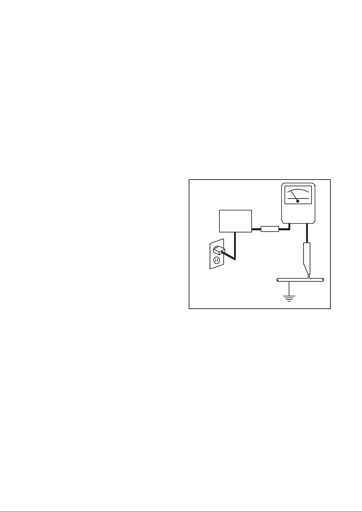
d. Leakage Current Hot Check - With the
instrument completely reassembled, plug the
AC line cord directly into a 230 V AC outlet. (Do
not use an isolation transformer during this
test.) Use a leakage current tester or a
metering system that complies with American
National Standards Institute (ANSI) C101.1
Leakage Current for Appliances and
Underwriters Laboratories (UL) 1410, (50.7).
With the instrument AC switch first in the on
position and then in the off position, measure
from a known earth ground (metal water pipe,
conduit, etc.) to all exposed metal parts of the
instrument (antennas, handle brackets, metal
cabinet, screw heads, metallic overlays, control
shafts, etc.), especially any exposed metal
parts that offer an electrical return path to the
chassis. Any current measured must not
exceed 0.5 milli-ampere. Reverse the
instrument power cord plug in the outlet and
repeat the test.
READING SHOULD
NOT BE ABOVE 0.5 mA
LEAKAGE
DEVICE
BEING
TESTED
TEST ALL EXPOSED
METAL SURFACES
ALSO TEST WITH
PLUG REVERSED
USING AC
ADAPTER PLUG
AS REQUIRED
ANY MEASUREMENTS NOT WITHIN THE
LIMITS SPECIFIED HEREIN INDICATE A
POTENTIAL SHOCK HAZARD THAT MUST
BE ELIMINATED BEFORE RETURNING THE
INSTRUMENT TO THE CUSTOMER OR
BEFORE CONNECTING THE ANTENNA OR
ACCESSORIES.
2. Read and comply with all caution and safety-
related notes on or inside the receiver cabinet, on
the receiver chassis, or on the LCD module.
3. Design Alteration Warning - Do not alter or add
to the mechanical or electrical design of this LCD
TV receiver. Design alterations and additions,
including, but not limited to circuit modifications
and the addition of items such as auxiliary audio
and/or video output connections, might alter the
safety characteristics of this receiver and create a
hazard to the user. Any design alterations or
additions will void the manufacturer's warranty and
may make you, the servicer, responsible for
personal injury or property damage resulting
therefrom.
CURRENT
TESTER
+
EARTH
GROUND
_
2-1 LTVP_ISP
Page 5

4. Hot Chassis Warning -
a. Some TV receiver chassis are electrically
connected directly to one conductor of the AC
power cord and maybe safety-serviced without
an isolation transformer only if the AC power
plug is inserted so that the chassis is
connected to the ground side of the AC power
source. To confirm that the AC power plug is
inserted correctly, with an AC voltmeter,
measure between the chassis and a known
earth ground. If a voltage reading in excess of
1.0V is obtained, remove and reinsert the AC
power plug in the opposite polarity and again
measure the voltage potential between the
chassis and a known earth ground.
b. Some TV receiver chassis normally have 85V
AC(RMS) between chassis and earth ground
regardless of the AC plug polarity. This chassis
can be safety-serviced only with an isolation
transformer inserted in the power line between
the receiver and the AC power source, for both
personnel and test equipment protection.
c. Some TV receiver chassis have a secondary
ground system in addition to the main chassis
ground. This secondary ground system is not
isolated from the AC power line. The two
ground systems are electrically separated by
insulation material that must not be defeated or
altered.
5. Observe original lead dress. Take extra care to
assure correct lead dress in the following areas: a.
near sharp edges, b. near thermally hot parts-be
sure that leads and components do not touch
thermally hot parts, c. the AC supply, d. high
voltage, and, e. antenna wiring. Always inspect in
all areas for pinched, out of place, or frayed wiring.
Check AC power cord for damage.
6. Components, parts, and/or wiring that appear to
have overheated or are otherwise damaged
should be replaced with components, parts, or
wiring that meet original specifications.
Additionally, determine the cause of overheating
and/or damage and, if necessary, take corrective
action to remove any potential safety hazard.
7. Product Safety Notice - Some electrical and
mechanical parts have special safety-related
characteristics which are often not evident from
visual inspection, nor can the protection they give
necessarily be obtained by replacing them with
components rated for higher voltage, wattage, etc..
Parts that have special safety characteristics are
identified by a ! on schematics and in parts lists.
Use of a substitute replacement that does not
have the same safety characteristics as the
recommended replacement part might create
shock, fire, and/or other hazards. The product's
safety is under review continuously and new
instructions are issued whenever appropriate.
Prior to shipment from the factory, our products
are strictly inspected to confirm they comply with
the recognized product safety and electrical codes
of the countries in which they are to be sold.
However, in order to maintain such compliance, it
is equally important to implement the following
precautions when a set is being serviced.
2-2 LTVP_ISP
Page 6

Precautions during Servicing
A. Parts identified by the ! symbol are critical for
safety.
Replace only with part number specified.
B. In addition to safety, other parts and assemblies
are specified for conformance with regulations
applying to spurious radiation. These must also be
replaced only with specified replacements.
Examples: RF converters, RF cables, noise
blocking capacitors, and noise blocking filters, etc.
C. Use specified internal wiring. Note especially:
1) Wires covered with PVC tubing
2) Double insulated wires
3) High voltage leads
D. Use specified insulating materials for hazardous
live parts. Note especially:
1) In sulation Tape
2) PVC tubing
3) Spacers
4) Insulators for transistors.
E. When replacing AC primary side components
(transformers, power cord, etc.), wrap ends of
wires securely about the terminals before
soldering.
F. Observe that the wires do not contact heat
producing parts (heat sinks, oxide metal film
resistors, fusible resistors, etc.)
G. Check that replaced wires do not contact sharp
edged or pointed parts.
H. When a powe r cord ha s been re place d, chec k th at
5~6 kg of force in any direction will not loosen it.
I. Also check areas surrounding repaired locations.
J. Use care that foreign objects (screws, solder
droplets, etc.) do not remain inside the set.
K. Crimp type wire connector
The power transformer uses crimp type
connectors which connect the power cord and the
primary side of the transformer. When replacing
the transformer, follow these steps carefully and
precisely to prevent shock hazards.
Replacement procedure
1) Remove the old connector by cutting the wires
at a point close to the connector.
Important: Do not re-use a connector (discard
it).
2) Strip about 15 mm of the insulation from the
ends of the wires. If the wires are stranded,
twist the strands to avoid frayed conductors.
3) Align the lengths of the wi res to be connected.
Insert the wires fully into the connector.
4) Use the crimping tool to crimp the metal sleeve
at the center position. Be sure to crimp fully to
the complete closure of the tool.
L. When connecting or disconnecting the internal
connectors, first, disconnect the AC plug from the
AC supply outlet.
M. When installing parts or assembling the cabinet
parts, be sure to use the proper screws and
tighten certainly.
2-3 LTVP_ISP
Page 7
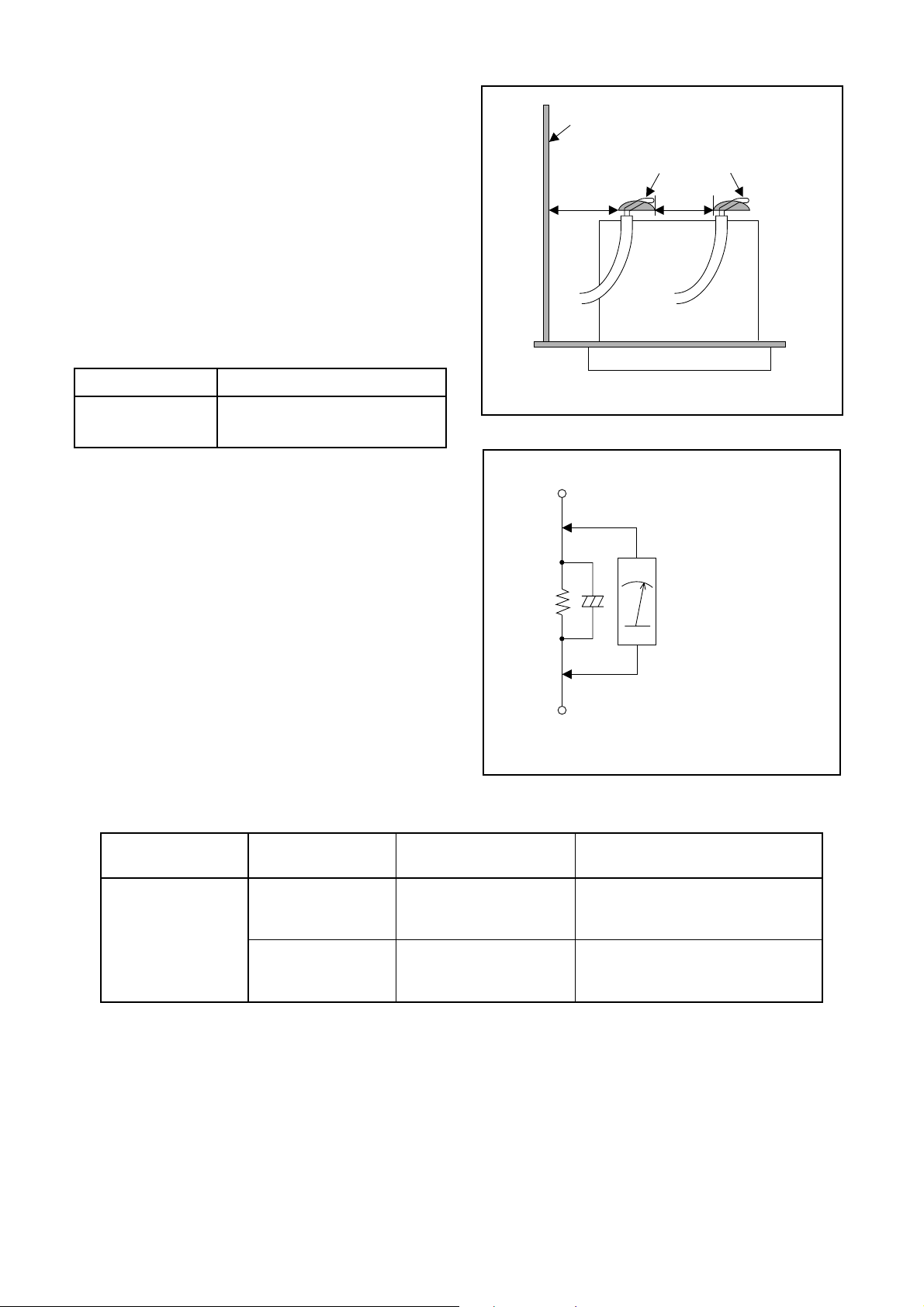
Safety Check after Servicing
Examine the area surrounding the repaired location
for damage or deterioration. Observe that screws,
parts and wires have been returned to original positions. Afterwards, perform th e following t ests and c onfirm the specifi ed values in order to verify c ompliance
with safety standards.
1. Clearance Distance
When replacing primary circuit components, confirm
specified clearance dis tance (d) and (d') between sol dered terminals, and between terminals and surrounding metallic parts. (See Fig. 1)
Table 1 : Ratings for selected area
AC Line Voltage Clearance Distance (d), (d’)
230 V
Note: This table is unofficial and for reference only.
Be sure to confirm the precis e values.
≥ 3mm(d)
≥ 6 mm(d’)
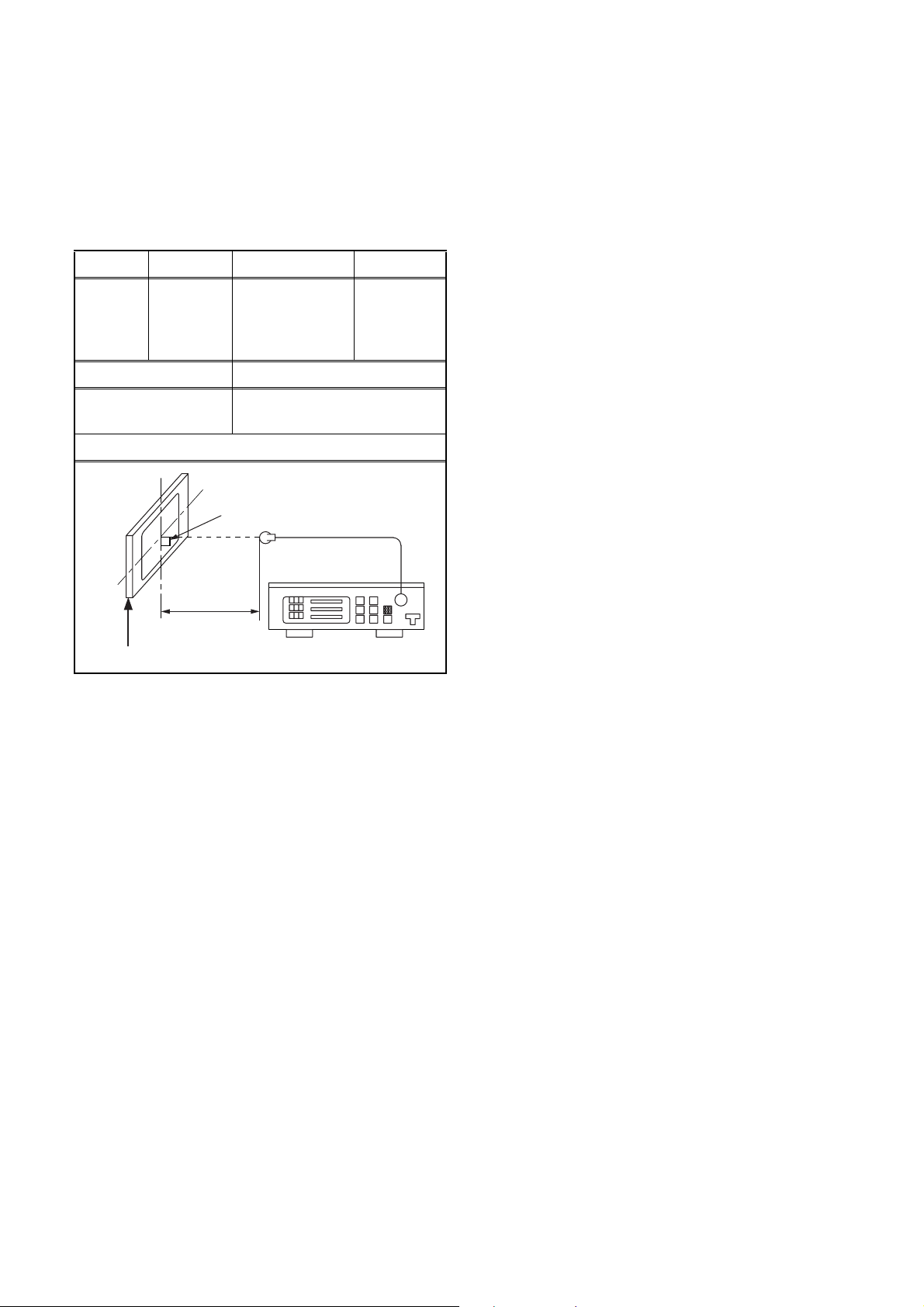
2. Leakage Current Test
Confirm the specified (or lower) leakage current between B (eart h ground, power cord plug prongs) and
externally exposed accessible parts (RF terminals, antenna terminals, video and audio in put and outpu t terminals, microphone jacks, earphone jacks, etc.).
Chassis or Secondary Conductor
Primary Circuit
d' d
Exposed Accessible Part
Z
AC Voltmeter
(High Impedance)
Fig. 1
Measuring Method : (Power ON)
Insert load Z between B (earth ground, power cord
plug prongs) and exposed accessible parts. Use an
AC v olt mete r to me asur e acr oss bo th termina ls of load
Z. See Fig. 2 and following table.
Table 2: Leakage current ratings for selected areas
AC Line Voltage Load Z Leakage Current (i)
2kΩ RES.
Connected in
parallel
230 V
50kΩ RES.
Connected in
parallel
Note: This table is unofficial and for reference only. Be sure to confirm the precise values.
i≤0.7mA AC Peak
i≤2mA DC
i≤0.7mA AC Peak
i≤2mA DC
One side of
B
Power Cord Plug Prongs
One side of power cord plug
prongs (B) to:
Antenna terminals
A/V Input, Output
Fig. 2
RF or
2-4 LTVP_ISP
Page 8
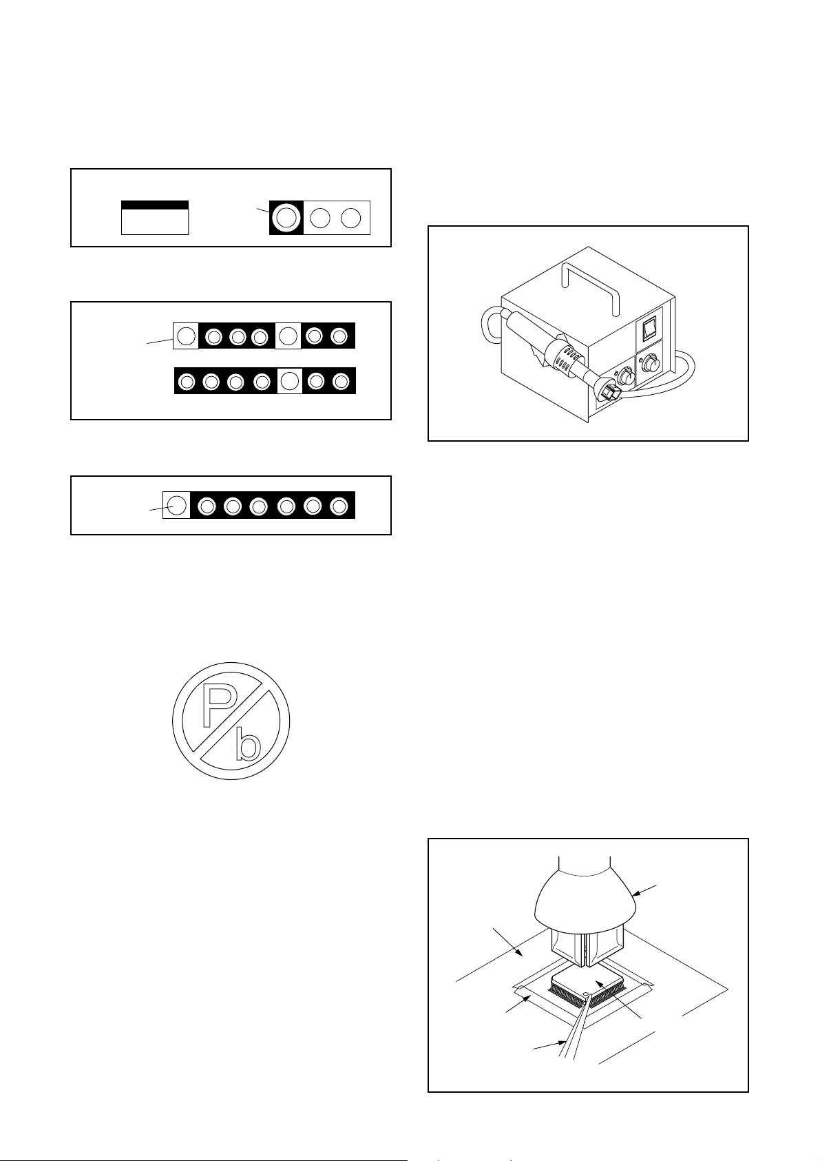
STANDARD NOTES FOR SERVICING
Circuit Board Indications
1. The output pin of the 3 pin Regulator ICs is
indicated as shown.
Top View
Out
2. For other ICs, pin 1 and every fifth pin are
indicated as shown.
Pin 1
3. The 1st pin of every male connector is indicated as
shown.
Pin 1
Input
In
Bottom View
5
10
Pb (Lead) Free Solder
Pb free mark will be found on PCBs which use Pb
free solder . (Re fer to figure.) Fo r PCBs with Pb fre e
mark, be sure to use Pb free solder. For PCBs
without Pb free mark, use standard solder.
Pb free mark
How to Remove / Install Flat Pack-IC
1. Removal
With Hot-Air Flat Pack-IC Desoldering Machine:
1. Prepare the hot-air flat pack-IC desoldering
machine, then apply hot air to the Flat Pack-IC
(about 5 to 6 seconds). (Fig. S-1-1)
Fig. S-1-1
2. Remove the flat pack-IC with tweezers while
applying the hot air.
3. Bottom of the flat pack-IC is fixed with glue to the
CBA; when removing entire flat pack-IC, first apply
soldering iron to center of the flat pack-IC and heat
up. Then remove (glue will be melted). (Fig. S-1-6)
4. Release the flat pack-IC from the CBA using
tweezers. (Fig. S-1-6)
CAUTION:
1. The Flat Pack-IC shape may differ by models. Use
an appropriate hot-air flat pack-IC desoldering
machine, whose shape matches that of the Flat
Pack-IC.
2. Do not supply hot air to the chip parts around the
flat pack-IC for over 6 seconds because damage
to the chip parts may occur. Put masking tape
around the flat pack-IC to protect other parts from
damage. (Fig. S-1-2)
3. The flat pack-IC on the CBA is affixed with glue, so
be careful not to break or damage the foil of each
pin or the solder lands under the IC when
removing it.
Hot-air
Flat Pack-IC
Desoldering
CBA
Masking
Tape
Tweezers
3-1 TVP_SN
Machine
Flat Pack-IC
Fig. S-1-2
Page 9
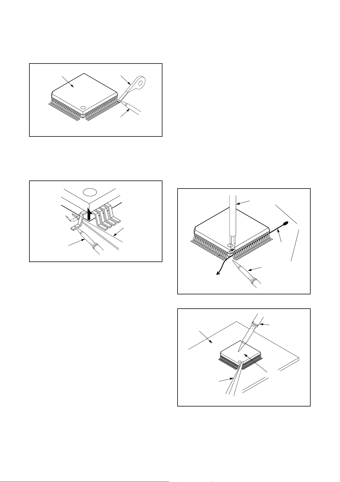
With Soldering Iron:
1. Using desoldering braid, remove the solder from
all pins of the flat pack-IC. When you use solder
flux which is applied to all pins of the flat pack-IC,
you can remove it easily. (Fig. S-1-3)
Flat Pack-IC
Desoldering Braid
Soldering Iron
Fig. S-1-3
2. Lift each lead of the flat pack-IC upward one by
one, using a sharp pin or wire to which solder will
not adhere (iron wire). When heating the pins, use
a fine tip soldering iron or a hot air desoldering
machine. (Fig. S-1-4)
With Iron Wire:
1. Using desoldering braid, remove the solder from
all pins of the flat pack-IC. When you use solder
flux which is applied to all pins of the flat pack-IC,
you can remove it easily. (Fig. S-1-3)
2. Affix the wire to a workbench or solid mounting
point, as shown in Fig. S-1-5.
3. While heating the pins using a fine tip soldering
iron or hot air blower, pull up the wire as the solder
melts so as to lift the IC leads from the CBA
contact pads as shown in Fig. S-1-5.
4. Bottom of the flat pack-IC is fixed with glue to the
CBA; when removing entire flat pack-IC, first apply
soldering iron to center of the flat pack-IC and heat
up. Then remove (glue will be melted). (Fig. S-1-6)
5. Release the flat pack-IC from the CBA using
tweezers. (Fig. S-1-6)
Note: When using a soldering iron, care must be
taken to ensure that the flat pack-IC is not
being held by glue. When the flat pack-IC is
removed from the CBA, handle it gently
because it may be damaged if force is applied.
Sharp
Pin
Fine Tip
Soldering Iron
3. Bottom of the flat pack-IC is fixed with glue to the
CBA; when removing entire flat pack-IC, first apply
soldering iron to center of the flat pack-IC and heat
up. Then remove (glue will be melted). (Fig. S-1-6)
4. Release the flat pack-IC from the CBA using
tweezers. (Fig. S-1-6)
Fig. S-1-4
To Solid
Mounting Point
CBA
Hot Air Blower
or
Iron Wire
Soldering Iron
Fig. S-1-5
Fine Tip
Soldering Iron
Flat Pack-IC
Tweezers
Fig. S-1-6
3-2 TVP_SN
Page 10
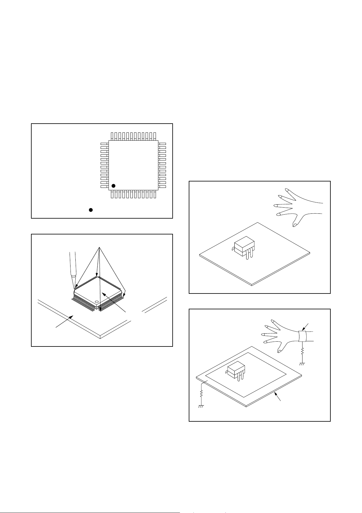
2. Installation
1. Using desoldering braid, remove the solder from
the foil of each pin of the flat pack-IC on the CBA
so you can install a replacement flat pack-IC more
easily.
2. The “●” mark on the flat pack-IC indicates pin 1.
(See Fig. S-1-7.) Be sure this mark matches the 1
on the PCB when positioning for installation. Then
presolder the four corners of the flat pack-IC. (See
Fig. S-1-8.)
3. Solder all pins of the flat pack-IC. Be sure that
none of the pins have solder bridges.
Example :
Pin 1 of the Flat Pack-IC
is indicated by a " " mark.
Fig. S-1-7
Instructions for Handling Semiconductors
Electrostatic breakdown of the semi-cond uc tors may
occur due to a potential difference caused by
electrostatic charge during unpacking or repair work.
1. Ground for Human Body
Be sure to wear a grounding band (1 MΩ) that is
properly grounded to remove any static electricity that
may be charged on the body.
2. Ground for Workbench
Be sure to place a conductive sheet or copper plate
with proper grounding (1 MΩ) on the workbench or
other surface, where the semi-conductors are to be
placed. Because the static electricity charge on
clothing will not escape through the body grounding
band, be careful to avoid contacting semi-conductors
with your clothing.
<Incorrect>
CBA
Presolder
Flat Pack-IC
Fig. S-1-8
<Correct>
1MΩ
CBA
Grounding Band
1MΩ
CBA
Conductive Sheet or
Copper Plate
3-3 TVP_SN
Page 11
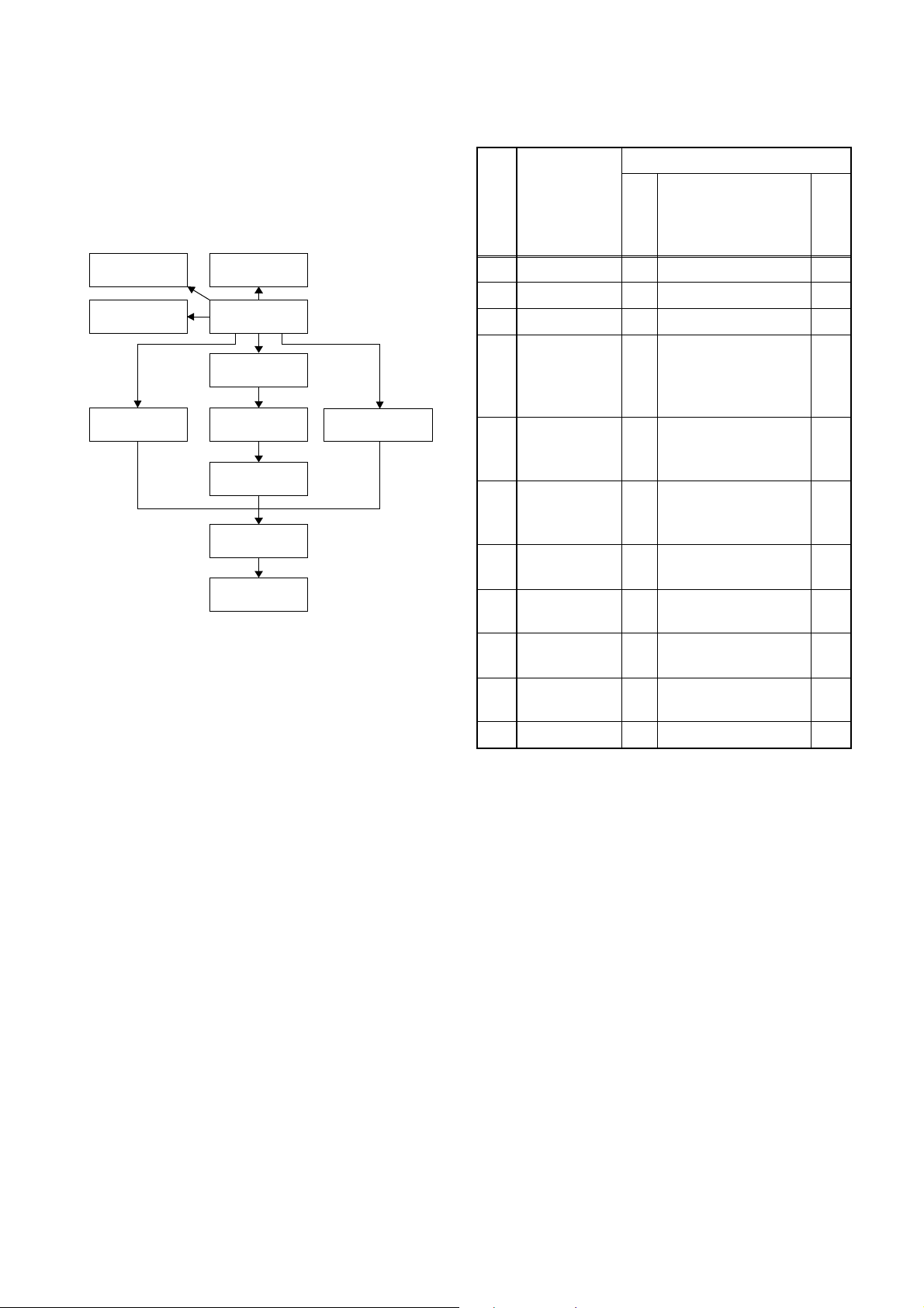
CABINET DISASSEMBLY INSTRUCTIONS
1. Disassembl y Flowchart
This flowchart indicates the disassembly steps fo r the
cabinet part s and the CBA in order to gain acces s to
item(s) to be ser vic ed. When r eassembling, follow the
steps in reverse order. Bend, route and dress the
cables as they were.
[9] IR Sensor
CBA
[10] Speaker (s)
[6] Inverter CBA
[8] Function CBA
[1] Rear Cabinet
[2] Jack Holder
[3] Jack Shield
[5] Main CBA
[7] LCD Module
Assembly
[11] Front
Cabinet
[4] LCD Main CBA
2. Disassembly Method
REMOVAL
ID/
LOC
.
PART
No.
[1] Rear Cabinet D1 11(S-1) --[2] Jack Holder D2 2(S-2), (S-3) --[3] Jack Shield D2 ---------- ---
LCD Main
[4]
CBA
[5] Main CBA
[6] Inverter CBA
LCD Module
[7]
Assembly
[8] Function CBA
REMOVE/
*UNHOOK/UNLOCK/
Fig.
No.
RELEASE/UNPLUG/
DESOLDER
3(S-4), *CN310A,
*CN311A, *CN313A,
D2
D3
*CN101B, *CN102B,
*CN103B
6(S-5), *CN801,
D2
*CN802, *CN405,
D3
*CN51, *CN53
6(S-6), *T1401,
D2
*T1402, *T1403,
D3
*T1404
D2
13(S-7) ---
D3
D2
3(S-8) ---
D3
Note
---
---
---
IR Sensor
[9]
CBA
[10] Speaker (s)
D2
2(S-9) ---
D3
D2
4(S-10) ---
D3
[11] Front Cabinet D2 --------------- ---
↓
(1)
↓
(2)
(3)
↓
↓
(4)
↓
(5)
(1):Order of ste ps in Procedure. When reass embling,
follow the steps in reverse order.These numbers
are also used as the Identif ica tion ( lo cat io n) No. of
parts in Figures.
(2):Parts to be removed or installed.
(3):Fig. No. showing Procedure of Part Location.
(4):Identification of part to be removed, unhooked,
unlocked, released, unplugged, unclamped, or
desoldered.
S=Screw, P=Spring, L=Locking Tab, CN=Connec-
tor, *=Unhook, Unlock, Release, Unplug, or Desol-
der
2(S-2) = two screws (S-2)
(5):Refer to the following Reference Notes in the
Table.
4-1 L4264DC
Page 12
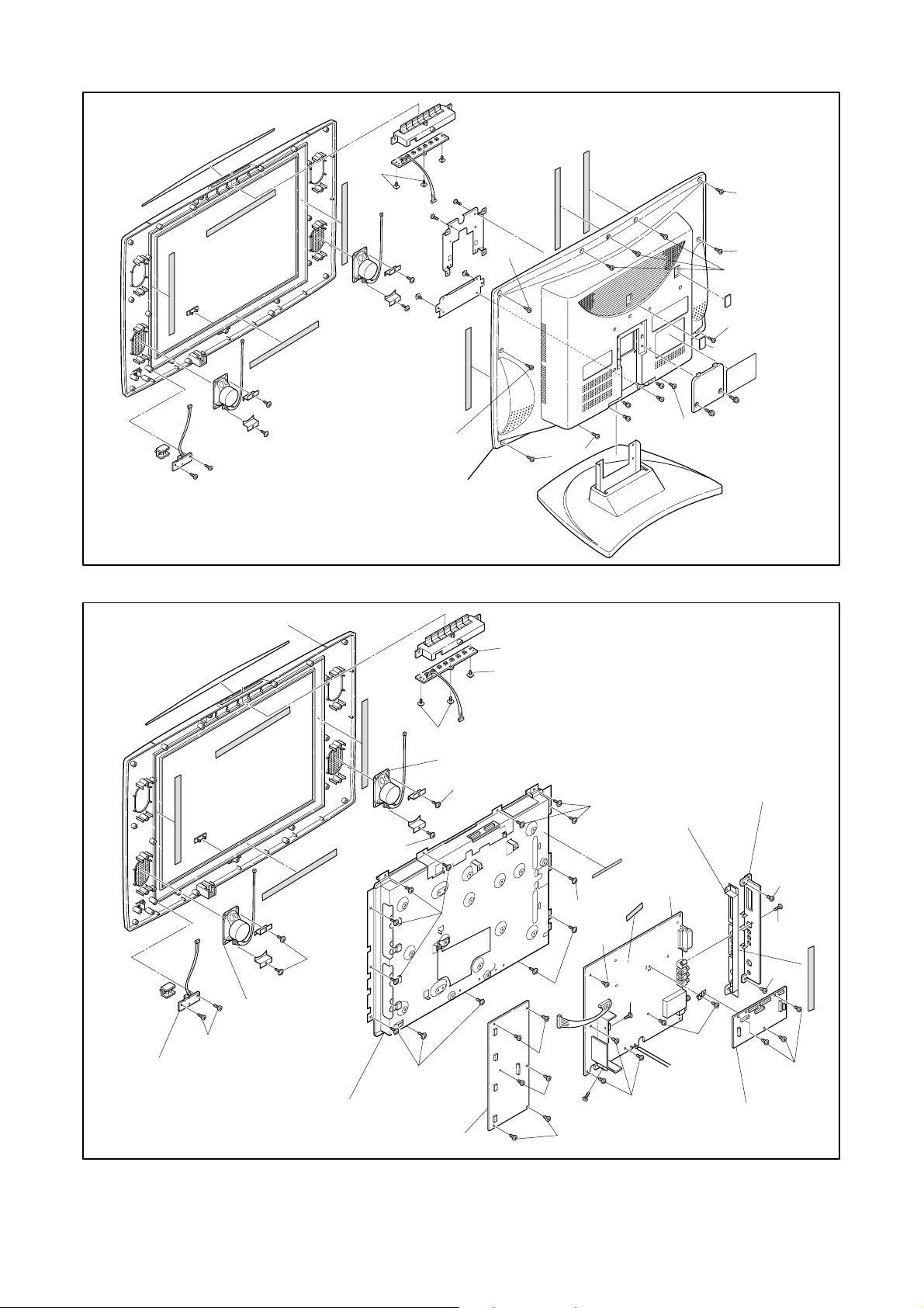
(S-1)
[11] Front Cabinet
(S-1)
[1] Rear Cabinet
(S-1)
(S-1)
[8] Function CBA
(S-8)
(S-1)
(S-1)
(S-1)
(S-1)
Fig. D1
(S-9)
[9] IR Sensor CBA
[7] LCD Module Assembly
(S-10)
[10] Speaker
(S-8)
[10] Speaker
(S-10)
(S-10)
(S-7)
(S-7)
[6] Inverter CBA
(S-7)
(S-6)
(S-6)
(S-7)
(S-6)
(S-7)
[3] Jack Shield
[5] Main CBA
(S-5)
(S-5)
[2] Jack Holder
(S-2)
(S-3)
(S-2)
(S-5)
(S-4)
[4] LCD Main CBA
Fig. D2
4-2 L4264DC
Page 13
Cable Wiring Diagram
To LCD Module Assembly
To LCD
Module
Assembly
To LCD
Module
Assembly
Inverter CBA
CN1403
CN1402
CN1401
CN1405
CN1404
LCD Main CBA
Main CBA
CN405
CN310A
CN301 CN104
CN101B
CN101A CN102A
CN801
CN311A
CN102B CN103B
CN103A
CN313A
CN53
CN105
CN51
CN802
To Speaker
CN51ACLN53
To Speaker
Function CBAIR Sensor CBA
Fig. D3
4-3 L4264DC
Page 14

HOW TO INITIALIZE THE LCD TELEVISION
To put the program back at the factory-default,
initialize the LCD television as the following procedure.
How to initialize the LCD television:
1. Turn the power on. (Use main power on the TV
unit.)
2. To enter the service mode, press [STANDBY], [2],
[7], [1], and [MUTE] buttons on the remote control
unit in that order within 5 seconds.
- To cancel the service mode, press [STANDBY]
button on the remote control.
3. To initialize the LCD television, press “DISPLAY”
button on the remote control unit.
4. Confirm "FF" indication on the upper right of the
screen.
5-1 L4100INT
Page 15
ELECTRICAL ADJUSTMENT INSTRUCTIONS
General Note:
“CBA” is abbreviation for “Circuit Board Assem-
bly.”
NOTE:
Electrical adjustment s are r equir e d after repl acing
circuit components and certain me chanical parts. It is
important to perform these adju stments on ly after all
repairs and replace ments have b een co mplete d.
Also, do not attempt these adjust ments unless th e
proper equipment i s ava ilab le.
Test Equipment Required
1. DC Voltmeter
2. Pattern Generator
3. Color Analyzer
How to Set up the Service mode:
1. Turn the power on. (Use main power on the TV
unit.)
2. Press [ST ANDBY], [2], [7], [1], and [MUTE] buttons
on the remote control unit in that order within 5
seconds.
- To cancel the service mode, press [STANDBY]
button on the remote control.
1. Initial Setting
General
Enter the Service mode.
Set the each initial data as shown on table 1 be low.
Table 1: Initial Data
BUTTON
ITEM
BRT(PAL)
CNT(PAL) 174
CLR-R(PAL) 74
CLR-B(PAL) 74
SHR(PAL) 143
S-BRT(PAL)
S-CNT(PAL) 174
S-CLR-R(PAL) 74
S-CLR-B(PAL) 74
S-SHR(PAL) 143
C-BRT(PAL)
C-CNT(PAL) 132
C-CLR-R(PAL) 154
C-CLR-B(PAL) 154
C-SHR(PAL) 143
BRT(SECAM)
CNT(SECAM) 174
CLR-R(SECAM) 74
CLR-B(SECAM) 74
SHR(SECAM) 143
S-BRT(SECAM)
S-CNT(SECAM) 174
S-CLR-R(SECAM) 74
S-CLR-B(SECAM) 74
S-SHR(SECAM) 143
C-BRT(SECAM)
C-CNT(SECAM) 132
C-CLR-R(SECAM) 154
C-CLR-B(SECAM) 154
C-SHR(SECAM) 143
BRT(NTSC)
CNT(NTSC) 174
CLR-R(NTSC) 70
CLR-B(NTSC) 70
TNT(NTSC) 148
SHR(NTSC) 143
S-BRT(NTSC)
S-CNT(NTSC) 174
S-CLR-R(NTSC) 70
S-CLR-B(NTSC) 70
S-TNT(NTSC) 148
S-SHR(NTSC) 143
(on the remote
control)
MENU → 1
MENU → 2
MENU → 3
MENU → 4
MENU → 5
MENU → 6
MENU → 7
MENU → 8
DAT A
VALUE
134
134
134
134
134
134
134
134
6-1 L4264EA
Page 16
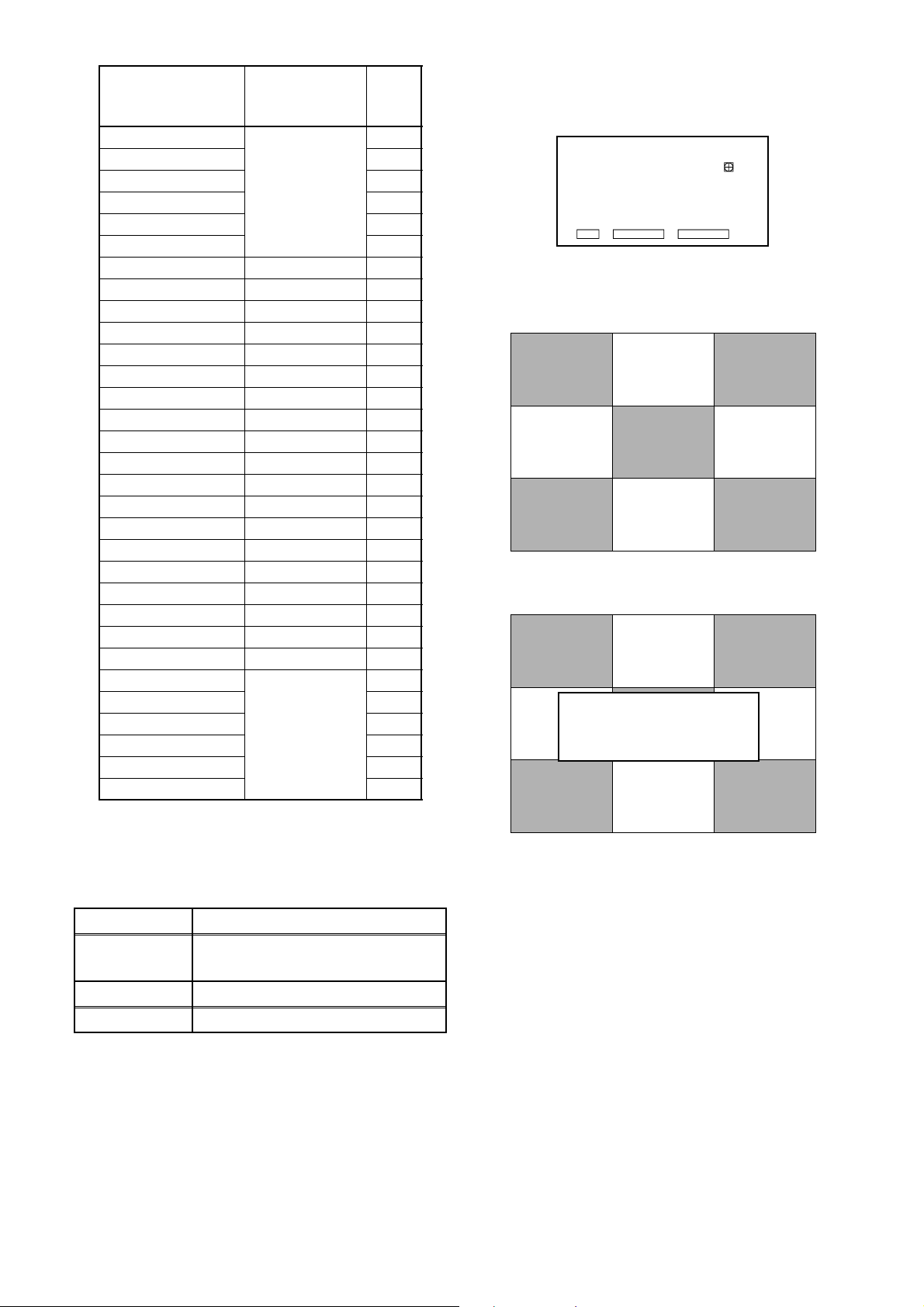
BUTTON
ITEM
C-BRT(NTSC)
C-CNT(NTSC) 132
C-CLR-R(NTSC) 154
C-CLR-B(NTSC) 154
C-TNT(NTSC) 148
C-SHR(NTSC) 143
BRIGHT 0 0
NORMAL 0 65
DARK 0 98
COR(C/D/S-1) VOL. p → 1 131
COG(C/D/S-1) VOL. p → 2 131
COB(C/D/S-1) VOL. p → 3 131
DR(C/D/S-1) VOL. p → 4 145
DG(C/D/S-1) VOL. p → 5 143
DB(C/D/S-1) VOL. p → 6 140
SBR(C/D/S-1) VOL. p → 70
SBB(C/D/S-1) VOL. p → 90
C-COR(C/D/S-2) VOL. p → 1 131
C-COG(C/D/S-2) VOL. p → 2 131
C-COB(C/D/S-2) VOL. p → 3 131
C-DR(C/D/S-2) VOL. p → 4 145
C-DG(C/D/S-2) VOL. p → 5 143
C-DB(C/D/S-2) VOL. p → 6 140
C-SBR(C/D/S-2) VOL. p → 70
C-SBB(C/D/S-2) VOL. p → 90
7F
LAST POWER OFF
SYSTEM
NCM ON
ASPECT OFF
RUSSIAN OFF
(on the remote
control)
MENU → 9
VOL. p
DAT A
VALUE
134
FF
PAL-BG
3. Flicker Adjustment
Adjustment Point: R977 (LCD Main CBA)
LCD Main CBA
R977
1. Enter the Service mode.
2. Press “2” button on the remote control unit.
The following screen appears.
3. If Flicker Adjustment is not fit, the screen become
the following.
FLASH
(Go and Off)
2. +B Adjustment
Purpose: To obtain correct operation.
Symptom of Misadjustment: The picture is da r k and
the unit does not operate correctly.
Test Point Adj. Point
TP401 (+B)
TP300 (GND)
M. EQ. Spec.
DC Voltmeter +21.0±0.3V DC
Note: TP401(+B), TP300(GND), VR649 --- Main CBA
1. Connect DC Volt Meter to TP401 and
TP300(GND).
2. Adjust VR649 so that the voltage of TP401
becomes +21.0±0.3V DC.
VR649
4. Adjust R977 so that flash stops.
6-2 L4264EA
Page 17
The following adjustment normally are not
attempted in the field. Only when replacing the
LCD Panel then adjust as a preparation.
4. White Balance Adjustment
Purpose: To m ix red, green a nd blue beam s co rrectly
for pure white.
Symptom of Misadjustment: White becomes bluish
or reddish.
Test Point Adj. Point Mode Input
[RF/AV2(CVBS)]
Screen
Pattern Generator,
Color analyzer
VOL. p
buttons
M. EQ. Spec.
C/D/S-1
[AV1(RGB)]
C/D/S-2
Figure
x: 260 to 320,
y: 270 to 330
White Purity
(APL 80%)
or
(APL 40%)
It carries out in a darkroom.
Perpendicularity
L = 3 cm
INPUT: WHITE 80%
1. Operate the unit for more than 20 minutes.
2. Input the White Purity (APL 80% or APL 40%).
3. Set the color analyzer to the CHROMA mode and
bring the optical receptor to the center on the
LCD-Panel surface after zero point calibration as
shown above.
Note: The optical receptor must be set
perpendicularly to the LCD Panel surface.
4. [RF/AV2(CVBS)]
Enter the Service mode. Press “VOL p” button on
the remote control unit and select “C/D/S-1” mode.
[AV1(RGB)]
Enter the Service mode. Press “VOL p” button on
the remote control unit and select “C/D/S-2” mode.
5. [RF/AV2(CVBS)]
When “x” value and “y” value are not within
specification, adjust “DB (C/D/S-1)” or “DR (C/D/S-
1)”. Refer to “1. Initial Setting.”
Note: “DB(C/D/S1)” or “DR(C/D/S1)” must be
adjusted within ±10.
[AV1(RGB)]
When “x” value and “y” value are not within
specification, adjust “C-DB(C/D/S-2)” or “C-DR(C/
D/S-2)”. Refer to “1. Initial Setting.”
Note: “C-DB(C/D/S-2)” or “C-DR(C/D/S-2)” must
be adjusted within ±10.
6. Turn the power off and on again. (Main power
button on the TV unit.)
Color Analyzer
6-3 L4264EA
Page 18

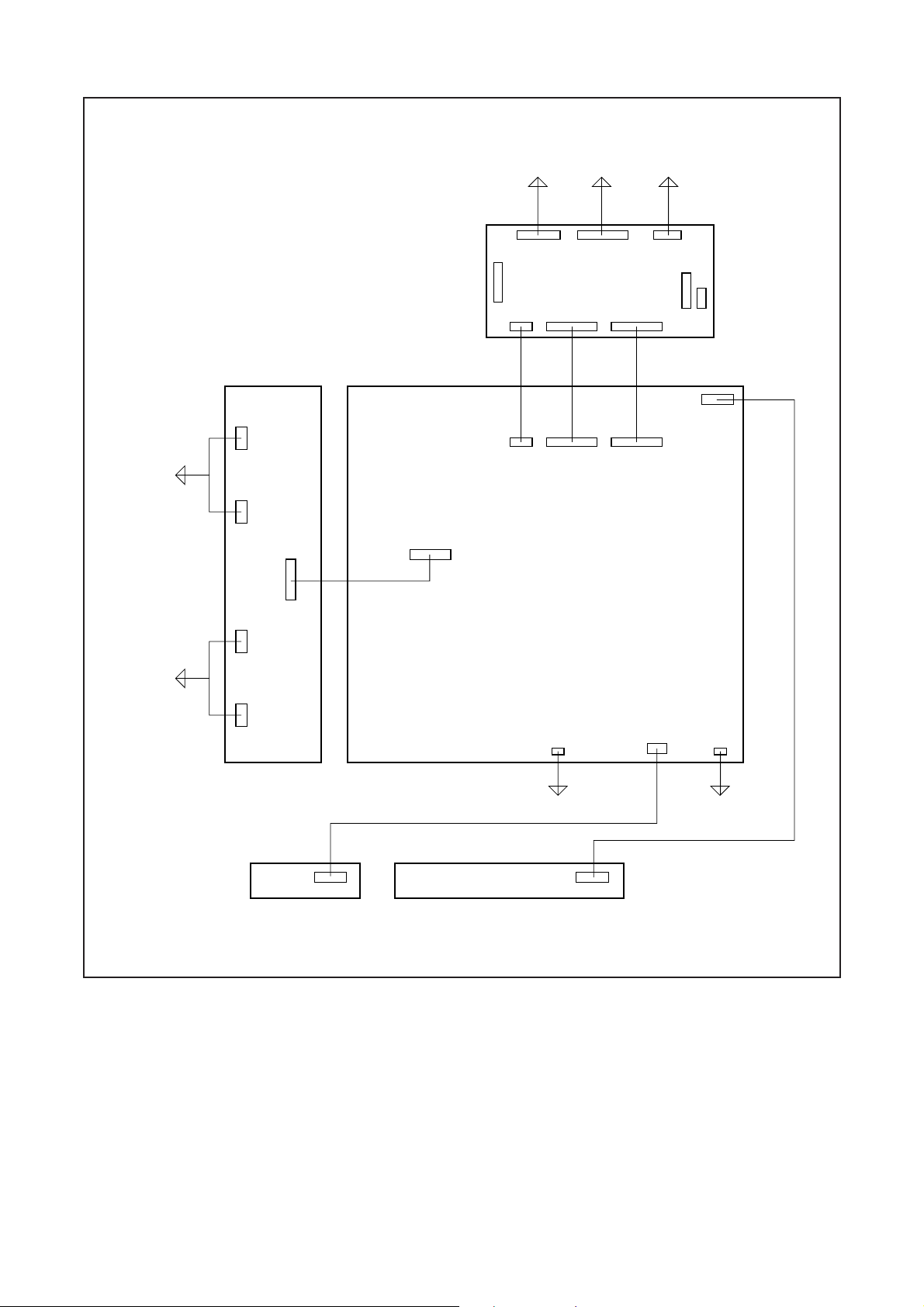
BLOCK DIAGRAMS
System Control Block Diagram
AL+5V
FUNCTION CBA
KEY SWITCH
KEY SWITCH
CN51A
KEY-IN-144
KEY-IN-233
CN51
STAND BY
IR SENSOR CBA
D51
SENSOR
REMOTE
RCV51
CLN53
RCV-IN33
CN53
BACKLIGHT-SW
BACKLIGHT-ADJ
CN1401
BACKLIGHT-ADJ
11 11
CN405
INVERTER CBA
TO LCD BACKLIGHT
BLOCK DIAGRAM
P-ON-H
PROTECT-1
P-ON-H13 13
BACKLIGHT-SW
PROTECT-112 12
10 10
CN102A
KEY-IN-144
KEY-IN-255
TO POWER SUPPLY
BLOCK DIAGRAM
P-ON-H
P-ON-H2
PROTECT-1
PROTECT-2
RCV-IN11
BACKLIGHT-SW
BACKLIGHT-ADJ
PROTECT-113 13
BUS-OPEN(NU)
33
22
20 20
P-25V-ON
PROTECT-3
P-ON-H66
PROTECT-214 14
AFT-IN11 11
P-ON-H222 22
PROTECT-316 16
TO IF/VIDEO
BLOCK DIAGRAM
SCL
SDA
S-SW
AFT-IN
INPUT-0
S/C-JACK-MUTE
VOLUME77
A-MUTE(NU)
INPUT-099
S-SW15 15
INPUT-110 10
SCL18 18
SDA19 19
88
INPUT-1
FBIN
RAPID-SW
P-25V-ON23 23
TO AUDI O
BLOCK DIAGRAM
SCL
SDA
VOLUME
SLOW-SW
SP-MUTE
INSEL-MUTE
S/C-JACK-MUTE
NICAM-RESET
MAIN CBALCD MAIN CBA UNIT
INSEL-MUTE
P-ON-L(NU)24 24
S/C-JACK-MUTE
16 16
SP-MUTE20 20
17 17
NICAM-RESET
FBIN25 25
22 22
SLOW-SW19 19
RAPID-SW18 18
RGB-CONTROL(NU)
26 26
X151
10MHz
IC151
(MICRO CONPUTER)
CN301(NO CONNECTION)
5
DVP-RESET-PC8DVP-CLK-PC
DVP-SOUT-PC6DVP-SIN-PC7DVP-CS-PC4MPSEL-0 3
13
XIN
BUS-OPEN 2
11
XOUT
AL+5V
5
RESET
IC153
IC301
(LCD DRIVE /
SIGNAL PROCESS)
4
10
RESET
2DVP-RESET
79
83
MPSEL-0
DVP-RESET-PC
2DVP-CLK
5
REG+3.3V
3.3V<-->5V
CONVERTER
Q152
57
DVP-CLK
3.3V<-->5V
Q153
CN102B
2DVP-SIN
4
CONVERTER
Q154
59
DVP-SIN
93
16
92
RCV-IN
KEY-IN-2
KEY-IN-1
2DVP-SOUT
3
3.3V<-->5V
CONVERTER
Q155
585060
DVP-SOUT
52
89
22
26BUS-OPEN(NU)
PROTECT-1
BACKLIGHT-SW
BACKLIGHT-ADJ
2DVP-CS
2
3.3V<-->5V
3.3V<-->5V
CONVERTER
Q156
DVP-CS
90756
88
PROTECT-2
PROTECT-3
H-SYNK
19
CONVERTER
7
89
QH
FBIN
59
P-ON-H
P-ON-H2
91
AFT-IN
24
46
277845
28
SCL
SDA
S-SW
INPUT-0
INPUT-1
VOLUME
RXD-FLASH
BUSY-FLASH
SCLK-FLASH
CE-FLASH(NU)
EPM-FLASH(NU)
3039314432
CN104(NO CONNECTION)
SCLK 3
BUSY 2
RXD 4
EPM(NU) 6
CE(NU) 5
CN103B CN103A
77
A-MUTE
CNVSS
TXD-FLASH
29
CNVSS 9
TXD 10
P-25V-ON
AL+5V
RESET 8
87
RAPID-SW-IN
IC152
(MEMORY)
23
SLOW-SW-IN
20
RGB-CONTROL(NU)
7
WP
1
838525
58
84INSEL-MUTE
SP-MUTE
P-ON-L(NU)
SC-VIDEO-MUTE
EEP-SDA
EEP-SCL
33
34
6
5
SCL
SDA
CN105(NO CONNECTION)
EEP-SCL 1
NICAM-RESET
EEP-SDA 2
BUS-OPEN 4
CN105 IS
USED FOR
ADJUSTMENT
AT FACTORY
7-1
L4264BLS
Page 19

IF/Video Block Diagram
VIDEO-Pr1
CN103A
VIDEO-Y2
TO
LCD BLOCKDIAGRAM
S-VIDEO-C5
VIDEO-Pb3
CN103B
CVBS18
S-VIDEO-Y6
CVBS29
AUDIO SIGNAL
MAIN CBA
VIDEO SIGNAL
TO AUDIO BLOCK
DIAGRAM
SIF
AUDIO
IC781 (INPUT SELECT)
Q781
3
BUFFER
4
5
WF8
SW
TO
AUDI O
BLOCK DIAGRAM
INPUT-0(INV)
INPUT-1(INV)
11
10
CONTROL
9
Q872
Q871
INPUT-0
INPUT-1
TO
SYSTEM CONTROL
BLOCK DIAGRAM
7
SIF
TU1
(TUNER UNIT)
6
AUDIO
17
16
AFT
VIDEO
9
SCL
Q744
WF6
BUFFER
Q752
15
VIDEO-Pr
WF5
BUFFER
Q751
11
VIDEO-Y
Q11
Q730
10
SDA
SCL
SDA
AFT-IN
RAPID-SW
TO SYSTEM
CONTROL
FBIN
BLOCK
DIAGRAM
Q734
SLOW-SW
S/C-JACK-MUTE
S-SW
JK722
VIDEO1
Q702
-IN
BUFFER
Q701
BUFFER
Q791
REG+5V
CY
JK721
S-VIDEO
-IN
Q743
Q792
JK751
8
SLOW-SW
Q731
16
RAPID-SW
Q753
19
VIDEO-OUT
WF2
WF3
BUFFER
7-2
WF7
WF4
BUFFER
BUFFER
Q754
7
20
VIDEO-IN
VIDEO-Pb
L4264BLIF
Page 20

Audio Block Diagram
AUDIO SIGNAL
SP802
SPEAKER
L-CH
SP801
SPEAKER
R-CH
QUASI-PEAK
CHANNEL MATRIX
AUTOMATIC
FM/AM
PRESCALE
dBX/MNR
PANDA1
I2C READ
REGISTER
QUASI-PEAK
DETECTOR
SOUND
SELECT
NICAM
PRESCALE
DEEMPHASIS
D/A
CONVERTER
VOLUME
SOUND
SELECT
AVC
SCART
PRESCALE
A/D
CONVERTER
LOUD SPEAKER
CHANNEL MATRIX
SCART1
CHANNEL
MATRIX
VOLUME
D/A
CONVERTER
SP-L 1
CN802
CLN802
GND 2
JK801
IC801 (AUDIO AMP)
HEADPHONE
JACK
11
AMP
MUTE
(L-CH)
6
VOLUME
/STANDBY
CONTROL
14
AMP
(R-CH)
1
WF1
RF
SP-R 1
CN801
7
2 5
CLN801
GND 2
TO SYSTEM
CONTROL
BLOCK
S/C-JACK-MUTE
SP-MUTE
INSEL-MUTE
VOLUME
TO IF/VIDEO
BLOCK
DIAGRAM
INPUT-0(INV)
INPUT-1(INV)
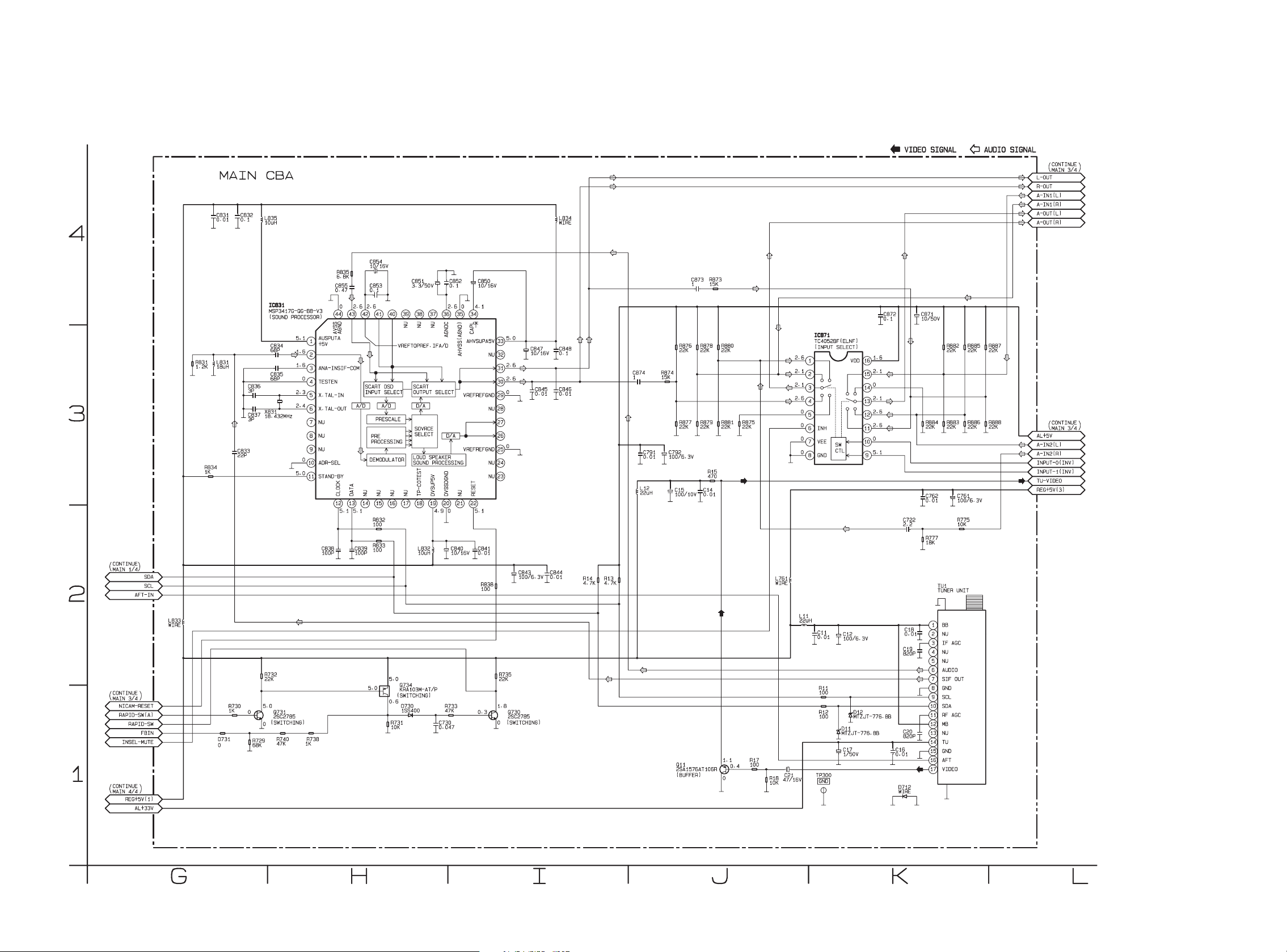
IC831 (SOUND PROCESSOR)
MAIN CBA
A/D
(R-CH)
TUNER
AUDIO1
4
2
3
AUDIO2
1
SW CTL
INH
9 10
6
JK751
Q733
Q732
6
AUDIO2(L)
-IN2AUDIO2(R)
-IN
Q741
1
AUDIO2(R)
-OUT
Q742
AL+5V
3
AUDIO2(L)
-OUT
13
I2C READ
REGISTER
STANDERD
AND SOUND
DETECTION
DEMODULATOR
CONVERTER
I2C
AGC
2
13
SDA
TO SYSTEM
CONTROL
DECORDER
RESET
12
22
SIF
SCL
NICAM-RESET
BLOCK
DIAGRAM
SCART DSP
INPUT SELECT
43
AUDIO
TO IF/VIDEO
BLOCK
DIAGRAM
SCART1 OUTPUT SELECT
L-CH
R-CH
30
31
TUNER
AUDIO2
AUDIO1
IC871 (INPUT SELECT)
111512
AUDIO1(L)
JK723
-IN
(L-CH)
JK724
AUDIO1(R)
-IN
7-3
L4264BLA
Page 21

LCD Block Diagram
LCD MODULE
OR(0)29
OR(1)28
OR(2)27
OR(3)26
OR(4)25
OR(5)24
OG(0)22
OG(1)21
OG(2)20
OG(3)19
OG(4)18
OG(5)17
OB(0)15
OB(1)14
OB(2)13
OB(3)12
OB(4)11
OB(5)10
ER(0)39
ER(1)38
ER(2)37
ER(3)36
ER(4)35
ER(5)34
EG(0)32
EG(1)31
EG(2)30
EG(3)29
EG(4)28
EG(5)27
EB(0)25
EB(1)24
EB(2)23
EB(3)22
EB(4)21
EB(5)20
VIDEO SIGNAL
LCD MAIN CBA UNIT
182
R
VIDEO
CVBSYC
CN310A
181
180
G
SIGNAL
179
OUTPUT
CONTROL
B
PROCESS
175
CN311A
TP322
TP323
174
173
169
168
167
166
R
NTSC/PAL
SEPARATION
165
BURST
161
160
G
LOCKED
TP318
159
TP319
155
158
CHROMA
DECODER
RCO
154
153
152
SECAM PDM
151
TP320
TP321
150
146
145
143
142
B
PAN E L
SIGNAL
PROCESS
TV
SIGNAL
PROCESS
85
84
XIN XOUT
X301
141
54MHz
140
139
TP316
TP317
135
134
133
132
131
R
130
129
128
TP312
TP313
121
120
127
123
122
G
119
116
115
TP314
TP315
114
113
106
B
IC301 (LCD DRIVE / SIGNAL PROCESS)
A/D
21
CN103B
VIDEO-Pr 1
A/D
33
44
2
VIDEO-Y
VIDEO-Pb 3
TO
IF/VIDEO
A/D
31
6
S-VIDEO-C 5
S-VIDEO-Y
BLOCK
DIAGRAM
A/D
134240
CVBS1 8
CVBS2 9
CN103A
INPUT
CONTROL
WF12
WF11
WF10
WF9
CN310A
LCD MODULE
STH1
POLLPCLKH1
979596
91
R904
R901
R902
LP 39
POL 38
STH1 37
ODDINV
105
R994
5
CLKH
ODDINV 8
EVENINV
STV1
104
103
EVENINV 2
CLKV
98
WF14
WF13
R905
R907
CN313A
STV1 14
PANEL+10.8V
VCOM
R977
Q971
IC981,
VCOM
CONTROL
2
CN311A
18
CLKV 16
VCOM 1
VCOM
VCOM 17
VCOM
VREF(0) 14
VREF(4) 10
VREF(1) 13
VREF(2) 12
VREF(3) 11
VREF(7) 6
VREF(5) 8
VREF(6) 7
VREF(8) 5
VREF(9) 4
7-4
L4264BLLCD
Page 22

Power Supply Block Diagram
REG+3.3V
REG+1.8V
AL+3.3V
CN103B
PANEL-6V
10 10 PANEL-6V
CN103A
AL+5V
+3.3V
REG
IC101
AL+8V14 14
AL+5V13 13
AL+3.3V11 11
Q508
+1.8V
IC102
AL+8V15 15
PANEL+10.8V
PANEL+25V
PANEL+3.3V
LCD MAIN CBA UNIT
CN101B
PANEL+25V
PANEL+3.3V
PANEL+10.8V
77
44
11
CN101A
REG
P-25V-ON
AL+3.3V
REG+5V
AL+8V
TO LCD BACKLIGHT
BLOCK DIAGRAM
AL+21V
P-ON-L
P-ON-H2
CN1401
AL+21V11
CN405
PROTECT-3
PROTECT-1
PROTECT-2
AL+5V
AL+33V
+12V
P-ON-H
INVERTER CBA
AL+21V33
AL+21V22
AL+21V44
Q501
Q511
Q511
Q502
IC631
15
(
D505
SHUNT
REGULATOR
(
14
5
CAUTION !
Fixed voltage (or Auto voltage selectable ) power supply circuit is used in this unit.
If Main Fuse (F601) is blown, check to see that all components in the power supply
circuit are not defective before you connect the AC plug to the AC power supply.
Otherwise it may cause some components in the power supply circuit to fail.
Q503
Q504
16
T601
CAUTION !
FOR CONTINUED PROTECTION AGAINST FIRE HAZARD,
REPLACE ONLY WITH THE SAME TYPE T 4A , 250 V FUSE.
HOT COLD
7
+5V
Q512
REG
Q505
12
IC504
+3.3V
13
REG
Q510
Q633
+5V
REG
IC507
+8V
REG
IC503
9
10
3
11
2
Q507
+B
TP401
1
4
(
D649
SHUNT
REGULATOR
(
IC603
ERROR
VOLTAGE
+B ADJ
VR649
1
4
IC601
2
3
ERROR
VOLTAGE
DET
MAIN CBA
2
3
DET
BRIDGE
RECTIFIER
D605
LINE
FILTER
L601
F601
AC601
AC CORD
T4A L 250V
NOTE :
The voltage for parts in hot circuit is measured using
HOT CIRCUIT. BE CAREFUL.
hot GND as a common terminal.
SWITCHING
REGULATOR
IC602
7-5
Q602
Q603
2
1
4
756
L4264BLP
Page 23

LCD Backlight Block Diagram
BACK
1
CN1402
LIGHT
2
OVER VOLTAGE
PROTECTOR
Q1410,1411
CN1403
OVER VOLTAGE
PROTECTOR
Q1412,1413
BACK
1
LIGHT
2
Q1414,1415
2
17
6
OVER VOLTAGE
PROTECTOR
BACK
LIGHT
BACK
LIGHT
LCD MODULEINVERTER CBA
1
2
CN1404
IC1403
(AMP)
+
1012
8
(AMP)
IC1402
-
+
-
+
5 3
-
9
5
+
7
-
6
3
+
1
-
2
1314
-
+
OVER VOLTAGE
PROTECTOR
Q1416,1417
Q1418,1419
1
2
CN1405
OVER VOLTAGE
PROTECTOR
OVER VOLTAGE
PROTECTOR
Q1420,1421
T1401
9
3
10
425
8
1
RL1401
457
OSC
T1403
Q1407,
LOGIC
9
3
Q1408
SW/
SW CTL
Q1401
OVER
VOLTAGE
10
425
+10V
REG.
28
VCC
PROTECT
7
6
T1402
Q1405,
Q1406
9
3
SW/
SW CTL
Q1403
10
425
8
IC1401 (DC-AC INVERTER CONTROL)
1
7
6
262723
OUTPUT
LOGIC1
24
OUTPUT
LOGIC2
7
8
1
6
14
PWM2
9
10
T1404
3
425
13
12
11
PWM1
7
8
1
6
9
10
SLOW
START
STANDBY
PROTECT
MODE SW
1
15
16
Q1402
AL+21V
P-ON-H
TO
POWER
SUPPLY
BLOCK
DIAGRAM
PROTECT-1
TO
SYSTEM
CONTROL
BACKLIGHT-SW
BLOCK
DIAGRAM
BACKLIGHT-ADJ
7-6
L4264BLLB
Page 24

SCHEMATIC DIAGRAMS / CBA'S AND TEST POINTS
Standard Notes
Many electrical and mechanical parts in this chassis have special characteristics. These characteristics often
pass unnoticed and the protection afforded by them cannot necessarily be obtained by using replacement
components rated for higher voltage, wattage, etc. Replacement parts that have these special safety
characteristics are identified in this manual and its supplements; electrical components having such features are
identified by the mark “!” in the schematic diagram and the parts list. Before replacing any of these components,
read the parts list in this manual carefully. The use of substitute replacement parts that do not have the same
safety characteristics as specified in the parts list may create shock, fire, or other hazards.
Notes:
1. Do not use the part number shown on these drawings for ordering. The correct part number is shown in the
parts list, and may be slightly different or amended since these drawings were prepared.
2. All resistance values are indi cated in ohms (K = 10
3. Resistor wattages are 1/4W or 1/6W unless otherwise specified.
4. All capacitance values are indicated in µF (P = 10
5. All voltages are DC voltages unless otherwise specified.
Note of Capacitors:
ML --- Mylar Cap. PP --- Metallized Film Cap. SC --- Semiconductor Cap. L --- Low Leakage type
Temperature Characteristics of Capacitors are noted with the following:
B --- ±10% CH --- 0±60 ppm/°C CSL --- +350~-1000 ppm/°C
3
, M = 106).
-6
µF).
Tolerance of Capacitors are noted with the following:
Z --- +80~-20%
Note of Resistors:
CEM --- Cement Res. MTL --- Metal Res. F --- Fuse Res.
Capacitors and transistors are represented by the following symbols.
CBA Symbols
(Top View) (Bottom View)
+
Electrolytic Capacitor
(Bottom View)
Transistor or Digital Transistor
E C B
(Top View)
NPN Transistor
E C B
(Top View)
(Top View)
PNP Transistor
E C B
(Top View)
Schematic Diagram Symbols
Digital Transistor
E C B
NPN Digital Transistor
PNP Digital Transistor
E C B
8-1 LC3P_SC
Page 25

LIST OF CAUTION, NOTES, AND SYMBOLS USED IN THE SCHEMATIC DIAGRAMS ON
THE FOLLOWING PAGES:
1. CAUTION:
FOR CONTINUED PROTECTION AGAINST FIRE HAZARD, REPLACE ONLY WITH THE SAME TYPE
FUSE.
2. CAUTION:
Fixed Voltage (or Auto voltage selectable) power supply circuit is used in this unit.
If Main Fuse (F601) is blown, first check to see that all components in the power supply circuit are not
defective before you connect the AC plug to the AC power supply. Otherwise it may cause some components
in the power supply circuit to fail.
3. Note:
1. Do not use the part number shown on the drawings for ordering. The correct part number is shown in the
parts list, and may be slightly different or amended since the drawings were prepared.
2. To maintain original function and reliability of repaired units, use only original replacement parts which are
listed with their part numbers in the parts list section of the service manual.
4. Voltage indications on the schematics are as shown below:
Plug the TV power cord into a standard AC outlet.:
2
(Unit: Volt)
1
5.0
(3.0)
3
(3.0)
5.0
Power on mode
Power off mode
5. How to read converged lines
1-D3
Distinction Area
Line Number
(1 to 3 digits)
Examples:
1. "1-D3" means that line number "1" goes to the line number
"1" of the area "D3".
2. "1-B1" means that line number "1" goes to the line number
"1" of the area "B1".
6. Test Point Information
: Indicates a test point with a jumper wire across a hole in the PCB.
: Used to indicate a test point with a component lead on foil side.
: Used to indicate a test point with no test pin.
: Used to indicate a test point with a test pin.
Voltage
Indicates that the voltage
is not consistent here.
3
2
1
AREA D3
1-B1
AREA B1
1-D3
ABCD
8-2 LC3P_SC
Page 26

Main 1/4 & IR Sensor Schematic Diagram
8-3
L4264SCM1
Page 27
Main 2/4 Schematic Diagram
8-4
L4264SCM2
Page 28

Main 3/4 Schematic Diagram
8-5 L4264SCM3
Page 29

Main 4/4 Schematic Diagram
CAUTION !
Fixed voltage (or Auto voltage selectable) power supply circuit is used in this unit.
If Main Fuse (F601) is blown , check to see that all components in the power supply
circuit are not defective before you connect the AC plug to the AC power supply.
Otherwise it may cause some components in the power supply circuit to fail.
CAUTION !
For continued protection against fire hazard,
replace only with the same type fuse.
NOTE:
The voltage for parts in hot circuit is measured using
hot GND as a common terminal.
8-6
L4264SCM4
Page 30

Function Schematic Diagram
8-7
L4264SCF
Page 31

Inverter Schematic Diagram
8-8
L4264SCINV
Page 32

LCD Main 1/2 Schematic Diagram
8-9
L4264SCL1
Page 33

LCD Main 2/2 Schematic Diagram
1 NOTE :
CN104, CN105, CN301 are used for adjustment at factory.
8-10
L4264SCL2
Page 34

Main CBA Top View
Because a hot chassis ground is present in the power
supply circut, an isolation transformer must be used.
Also, in order to have the ability to increase the input
slowly, when troubleshooting this type power supply
circuit, a variable isolation transformer is required.
CAUTION !
For continued protection against fire hazard,
replace only with the same type fuse.
NOTE:
The voltage for parts in hot circuit is measured using
hot GND as a common terminal.
WF1
PIN 14 OF
IC801
CAUTION !
Fixed voltage (or Auto voltage selectable) power supply circuit is used in this unit.
If Main Fuse (F601) is blown , check to see that all components in the power supply
circuit are not defective before you connect the AC plug to the AC power supply.
Otherwise it may cause some components in the power supply circuit to fail.
VR649
+B ADJ
TP401
+B
TP300
GND
8-11
BL4100F01013-1
Page 35

Main CBA Bottom View
Because a hot chassis ground is present in the power
supply circut, an isolation transformer must be used.
Also, in order to have the ability to increase the input
slowly, when troubleshooting this type power supply
circuit, a variable isolation transformer is required.
CAUTION !
For continued protection against fire hazard,
replace only with the same type fuse.
NOTE:
The voltage for parts in hot circuit is measured using
hot GND as a common terminal.
CAUTION !
Fixed voltage (or Auto voltage selectable) power supply circuit is used in this unit.
If Main Fuse (F601) is blown , check to see that all components in the power supply
circuit are not defective before you connect the AC plug to the AC power supply.
Otherwise it may cause some components in the power supply circuit to fail.
WF3
Q702
Emitter
WF2
Q701
Emitter
WF4
Q751
Emitter
WF5
Q752
Emitter
WF6
Q753
Emitter
WF7
Q754
Emitter
WF8
Q781
Emitter
8-12
BL4100F01013-1
Page 36

Function CBA Top View
IR Sensor CBA Top & Bottom View
Function CBA Bottom View
BL4100F01013-4
BL4100F01013-3
8-13
Page 37

Inverter CBA Top View
Inverter CBA Bottom View
8-14
BL4200F01011
Page 38

WAVEFORMS
AUDIO
0.1V
0.5ms
S-VIDEO-Y
0.2V
S-VIDEO-C
0.2V
0.5V
CVBS2
0.2V
0.5V
CVBS1
0.2V
0.5V
WF1 ~ WF8 = Waveforms to be observed at
Waveform check points.
(Shown in Schematic Diagram.)
Input: PAL Color Bar Signal (with 1kHz Audio Signal)
WF1 Pin 14 of IC801
AUDIO
0.1V
WF2 Q701 EMITTER
0.5ms
WF4 Q751 EMITTER
B 0.5V
WF5 Q752 EMITTER
5µs
WF7 Q754 EMITTER
CVBS2
0.2V
WF8 Q781 EMITTER
2020µ
s
S-VIDEO-Y
0.2V
WF3 Q702 EMITTER
S-VIDEO-C
0.2V
1010µ
2020µ
s
G 0.5V
2020µ
s
CVBS1
0.2V
2020µ
s
WF6 Q753 EMITTER
1010µ
s
s
R 0.5V
9-1
L4264WF
Page 39

WF9 ~ WF14 = Waveforms to be observed at
Waveform check points.
(Shown in Schematic Diagram.)
Input: PAL Color Bar Signal (with 1kHz Audio Signal)
WF9
R994
WF12
R904
CTKH 1V 20ns
WF10
R902
STH1 1V 1µs
WF11
R901
LP 1V 10µs
WF13
R907
STV1 1V 5ms
WF14
R905
POL 1V 20µs
9-2
CLKV 1V 10µs
L4264WF
Page 40

WIRING DIAGRAMS
LCD MAIN CBA UNIT
CN103B
VIDEO-Pb
S-VIDEO-Y
VIDEO-Y
GND
S-VIDEO-C
VIDEO-Pr
153
CN103A
VIDEO-Pr
CN102A
RCV-IN
132547689
RCV-IN
CN102B
2
VIDEO-Y
VIDEO-Pb
BACKLIGHT-SW
BACKLIGHT-ADJ
BACKLIGHT-SW
BACKLIGHT-ADJ
SP-R2GND
CN801
1
51342
4
GND
S-VIDEO-C
KEY-IN-1
KEY-IN-2
51342
KEY-IN-1
KEY-IN-2
6
6
S-VIDEO-Y
P-ON-H
6
P-ON-H
GND
GND
CVBS1
CVBS2
AL+3.3V
GND
AL+8V
AL+5V
12
11
11
GND
AL+3.3V
NU
AFT-IN
12
11
NU
AFT-IN
SP-L2GND
1
14
13
13
AL+8V
AL+5V
PROTECT-1
PROTECT-2
14
13
PROTECT-1
PROTECT-2
AL+8V
15
15
AL+8V
S-SW
15
S-SW
8
9
7
10
9
7
8
101412
GND
GND
CVBS1
CVBS2
VOLUME
A-MUTE(NU)
INPUT-0
INPUT-1
10131211141517161918212022
8
9
7
10
INPUT-0
INPUT-1
VOLUME
A-MUTE(NU)
CN802
INSEL-MUTE
S/C-JACK-MUTE
RAPID-SW
172220
18
16
18
16
17
RAPID-SW
INSEL-MUTE
S/C-JACK-MUTE
GND
PROTECT-3
SCL
172220
18
16
SCL
GND
PROTECT-3
JK751
NICAM-RESET
SP-MUTE
NU
SLOW-SW
P-25V-ON
231921
1923212022
NU
SP-MUTE
P-25V-ON
SLOW-SW
NICAM-RESET
NU
SDA
BUS-OPEN(NU)
NU
P-ON-H2
23
231921
NU
NU
SDA
P-ON-H2
BUS-OPEN(NU)
123456789
P-ON-L(NU)
RGB-CONTROL(NU)
FBIN
262425
262425
FBIN
P-ON-L(NU)
RGB-CONTROL(NU)
CN101ACN101B
NU
NU
PANEL+10.8V
GND
GND
132547689
252426
262425
GND
GND
PANEL+10.8V
1011121314151617181920
GND
GND
CN51A
CN51
GND
PANEL+3.3V
GND
PANEL+3.3V
GND
GND
132
1
2
GND
GND
GND
GND
689
51342
GND
GND
KEY-IN-2
AL+5V
KEY-IN-1
4
5
3
4
5
AL+5V
KEY-IN-2
KEY-IN-1
PANEL+25V
GND
GND
7
GND
GND
PANEL+25V
21
GND
6
6
GND
PANEL-6V
10
10
PANEL-6V
CN405
AL+21V
153
FUNCTION CBA
AL+21V
AL+21V
2
GND
AL+21V
4
GND
6
GND
7
CLN53
CN53
GND
8
AL+5VNUNU
1
2
NU
AL+5V
MAIN CBA
BACKLIGHT-SW
GND
9
10
GND
RCV-IN
51342
5
3
4
NU
GND
RCV-IN
TU1 TUNER UNIT
BACKLIGHT-ADJ
PROTECT-1
12
11
13
IR SENSOR CBA
AUDIO(R)
-IN
AUDIO(L)
-IN
VIDEO
-IN
S-VIDEO
IN
CLN801
SP801
SPEAKER
132547689
NU
VCOM
VCOM
CN313A
< NO CONNECTION >
AL+5V2BUSY3SCLK4RXD5NU6NU7GND8RESET9CNVSS10TXD
CN104
1
1325476
GND
CN301
MPSEL-0
BUS-OPEN
NU
VGH
VGH
DVP-CS-PC
DVP-CLK-PC
SVP-SOUT-PC
SP802
PANEL+3.3V
PANEL+3.3V
8
DVP-SIN-PC
DVP-RESET-PC
CLN802
SPEAKER
1013121114151716191820
NU
NU
PANEL-6V
PANEL-6V
PANEL-6V
CN311A
132547689
1
GND
CN310A
GND
GND
STV1
GND
PANEL-6V
2
3
GND4GND
EVENINV
AC601
CLKV
VREF(8)
VREF(9)
5
CLKH
AC CORD
GND
GND
VREF(6)
VREF(7)
6
GND7GND
13254
NU
GND
XDON
GND
VREF(5)
8
9
GND
ODDINV
GND
CN105
EEP-SCL
EEP-SDA
BUS-OPEN
CN105 IS
USED FOR
ADJUSTMENT
AT FACTORY
< NO CONNECTION >
VREF(3)
VREF(4)
VREF(2)
VREF(1)
VREF(0)
PANEL+10.8V
PANEL+10.8V
VCOM
VCOM
GND
101312111415171619182120222324272625282930
10
OB (5)11OB (4)12OB (3)13OB (2)14OB (1)15OB (0)
EB (5)
16
17
GND
OG (5)18OG (4)19OG (3)20OG (2)21OG (1)22OG (0)
CN1402
EB (4)
EB (3)
EB (2)
EB (1)
23
24
GND
OR (5)25OR (4)26OR (3)27OR (2)28OR (1)29OR (0)
1
BACK
EB (0)
153
AL+21V
CN1401
2
LIGHT
GND
2
AL+21V
EG (5)
EG (4)
4
6
GND
GND
GND
AL+21V
AL+21V
2
1
CN1403
BACK
LIGHT
EG (3)
EG (2)
EG (1)
EG (0)
GND
33
323134353736393840
30
31NU32
333435
GND
PANEL+3.3V
PANEL+3.3V
PANEL+3.3V
978
10
GND
GND
BACKLIGHT-SW
1
CN1404
BACK
ER (5)
ER (4)
ER (3)
36NU37
PANEL+3.3V
PANEL+3.3V
BACKLIGHT-ADJ
2
LIGHT
ER (2)
STH1
121113
PROTECT-1
ER (1)
38
POL
P-ON-H P-ON-H
ER (0)
GND
39LP40
GND
1
CN1405
BACK
INVERTER CBA
2
LIGHT
< NO CONNECTION >
10-1
LCD MODULE
L4264WI
Page 41

Cabinet
EXPLODED VIEWS
B6
A2
A3
B6
B6
A1
SP802
B6
L4
L1
CLN802
B14
L1
A7
Function CBA
L4
A
LCD1
B
L1
L1
L14
L1
C
Main CBA
B12
B21
B19
B3
B4
L3
B21
L2
L2
L2
L2
B21
L7
A4
L2
L2
A8
L2
L2
A10
L2
A10
A6
L19
A5
IR Sensor CBA
See Electrical Parts List
for parts with this mark.
SP801
L13
B14
L1
CLN801
L1
L1
Inverter CBA
L3
L3
L3
L1
B22
L20
L3
L16
L3
B10
AC601
B15
L3
L9
L3
L3
LCD Main CBA
L3
L3
B23
CN311A
CN310A
B
A
A9
CN313A
C
11-1 L4264CEX
Page 42
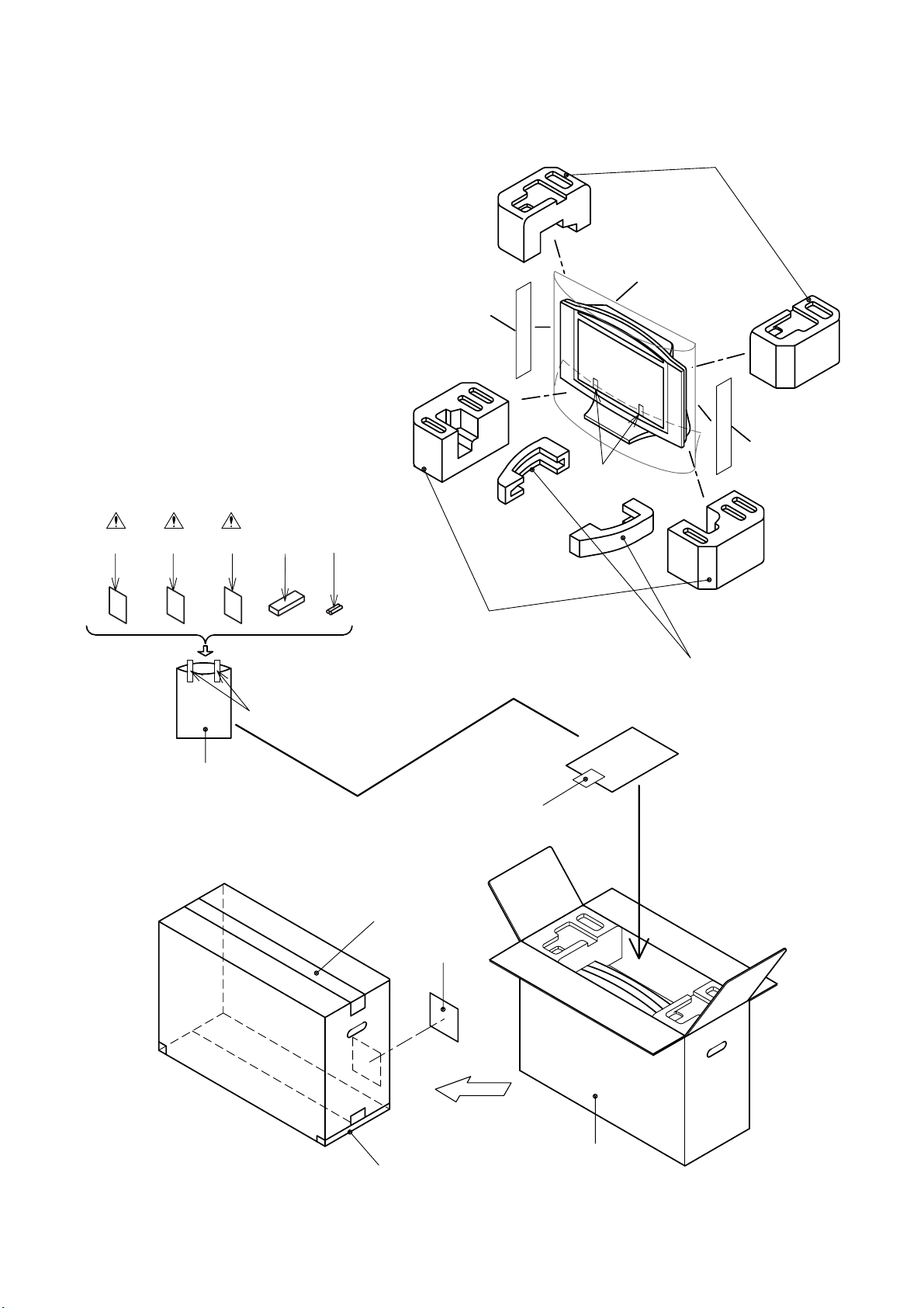
Packing
Some Ref. Numbers are
not in sequence.
Pac king Tape
Tape
S2
S4
Packing
Tape
X2-1 X2-3 X2-6
X1
X3
Tape
X5
S3
S6
Pac king Tape
Pac king Tape
S5
Pac king Tape
11-2 L4264PEX
FRONT
S1
Page 43
MECHANICAL PARTS LIST
PRODUCT SAFETY NOTE: Products marked with a
! have special characteristics important to safety.
Before replacing any of these components, read
carefully the product safety notice in this service
manual. Don't degrade the safety of the product
through improper servicing.
NOTE: Parts that are not assigned part numbers
(---------) are not available.
Ref. No. Description Part No.
A1 FRONT CABINET L4200EA 1EM020125
A2 BRAND BADGE L0230JA~FUNAI~ 0EM409021A
A3 CONTROL PLATE L4200EA 1EM220077
A4 REAR CABINET L4200EA 1EM020116
A5 SENSOR/LED LENS L0301UB 1EM220004
A6! RA TING LABEL L4264EE ---------A7 FUNCTION KNOB L4200EA 1EM320157
A8 REAR COVER L4200EA 1EM320158
A9 TIL T STAND ASSEMBL Y L0301UB 1EMN20039A
A10 CONNECTER CAP L4200EA 1EM420585
B3 20V ST AND HOLDER L4200EA 1EM320141
B4 JAC K HOLDE R L4100E A 1EM 120097
B6 CLOT H(15X19 0XT 0. 5) L0100J A 0EM407894
B12 20V TILT ST AND HOLDER L4200EA 1EM320145
B14 SPEAKER HOLDER L0110UA 0EM407855C
B19 JACK SHIELD L4100EA 1EM320140
B21 CLOTH(10X180XT0.5) L0336JG 0EM408827
B23 CLOTH(12X125X T 0.5) L010 1JB 0EM408489
CLN801 SPEAKER WIRE WX1L4200-003 WX1L4200-003
CLN802 SPEAKER WIRE 2P 2P WX1L0300-007
L1 SCREW P-TIGHT 3X12 WASHER HEAD+ GCJP3120
L2 SCREW P-TIGHT 3X12 BIND HEAD+ BLK GBHP3120
L4 SCREW P-TIGHT M3*10 WASHERHEAD+ GCJP3100
L7 DOUBLE SEMS SCREW M4X12 + BLAK FPH34120
L13 SCREW P-TIGHT M3*12 BIND+ GBJP3120
L14 SCREW P-TIGHT M3X8 BIND HEAD+ GBJP3080
L19 DOUBLE SEMS SCREW M4X9 + BLACK
LCD1 LCD MODULE ASSEMBL Y UC000XF 1FSA10101
SP801 SPEAKER S0407F10 DSD0807XQ002
SP802 SPEAKER S0407F10 DSD0807XQ002
L0130U A
PACKING
S1 CARTON L4264EE 1EM422444
S2 STYROFOAM T OP L0301UB 1EM020018A
S3 STYROFOAM BO TT OM L0301UB 1EM020019A
S4 SET BAG L0301UB 1EM320014
S5 SERIAL NO. LABEL L4200EA ---------S6 STYROFOAM STAND BOTTOM L0301UB 1EM020020A
S20 BAG REMOCON STD REMOCON 0VM406766
ACCESSORIES
X1 BAG PO LYETHYLENE 235X36 5XT0. 03 0EM408420
X3 REMOTE CONTROL 192/E RC001/N E309R D NE309RD
X5 DRY BATTERY R6P/2S or XB0M451T0001
DRY BATTERY(SUNRISE) R6SSE/2S XB0M451MS002
X2-1! OWNERS MANUAL L4264EE 1EMN21269
X2-3! OWNERS MANUAL L4264EE 1EMN21270
X2-6! OWNERS MANUAL L4264EE 1EMN21271
0EM408146A
20051220 12-1 L4264CA
Page 44
ELECTRICAL PARTS LIST
PRODUCT SAFETY NOTE: Products marked with a
! have special characteristics important to safety.
Before replacing any of these components, read
carefully the product safety notice in this service
manual. Don't degrade the safety of the product
through improper servicing.
NOTES:
1. Parts that are not assigned part numbers (---------)
are not available.
2. Tolerance of Capacitors and Resistors are noted
with the following symbols.
C.....±0.25% D.....±0.5% F.....±1%
G.....±2% J......±5% K.....±10%
M.....±20% N.....±30% Z.....+80/-20%
LCD MAIN CBA UNIT
Ref. No. Description Part No.
LCD MAIN CBA UNIT 1ESA11998
MMA CBA
Ref. No. Description Part No.
MMA CBA
Consists of the following:
MAIN CBA
FUNCTION CBA
IR SENSOR CBA
MAIN CBA
Ref. No. Description Part No.
MAIN CBA
Consists of the following
CAPACITORS
C11 CHIP CERAMIC CAP .(1608) B K 0.01µF/ 50V CHD1JK30B10 3
C12 ELECTROL YTIC CAP. 100µF/ 6.3V M or CE0KMASDL101
ELECTROLYTIC CAP . 100µF/ 6.3V M or CA0K101SP085
ELECTROLYTIC CAP . 100µF/ 6 .3V M CE0KMASTM101
C14 CHIP CERAMIC CAP .(1608) B K 0.01µF/ 50V CHD1JK30B10 3
C15 ELECTROL YTIC CAP. 100µF/ 10V M or CE1AMASDL101
ELECTROLYTIC CAP . 100µF/ 10V M or CA1A101SP085
ELECTROLYTIC CAP . 100µF/ 1 0V M CE1AMASTM101
C16 CHIP CERAMIC CAP .(1608) B K 0.01µF/ 50V CHD1JK30B10 3
C17 ELECTROL YTIC CAP. 1µF/ 50V M or CE1JMASDL1R0
ELECTROLYTIC CAP 1µF/ 50V M or CA1J1R0SP085
ELECTROLYTIC CAP 1µF/ 50V M CE1JMASTM1R0
C18 CHIP CERAMIC CAP .(1608) B K 0.01µF/ 50V CHD1JK30B10 3
C19 CHIP CERAMIC CAP . B K 820pF/50V CHD1JK30B821
C20 CHIP CERAMIC CAP . B K 820pF/50V CHD1JK30B821
C21 ELECTROL YTIC CAP. 47µF/ 16V M or CE1CMASDL470
ELECTROLYTIC CAP . 47µF/ 16 V M or CA1C470 SP085
ALUMINUM ELECTROL YT IC CAP 47µF/ 16V M CE1CMASTM470
C501 ELECTROL YTIC CAP. 22µF/ 50V M or CE1JMASDL 220
ELECTROLYTIC CAP . 22µF/ 50 V M or CA1J220S P085
ELECTROLYTIC CAP 22µF/ 50V M CE1JMASTM220
C502 CHIP CERAMIC CAP.(1608) B K 0.01µF/ 50V CHD1JK30B10 3
C503 CHIP CERAMIC CAP.(1608) B K 0.1µF/ 50V CHD1JK30B104
C505 ELECTROL YTIC CAP. 220µF/ 16V M or CE1CMASDL221
ELECTROLYTIC CAP . 220µF/ 16V M or CA1C221SP085
ELECTROLYTIC CAP . 220µF/ 16V M CE1CMASTM221
C506 CHIP CERAMIC CAP.(1608) B K 0.01µF/ 50V CHD1JK30B10 3
1ESA11996
----------
----------
----------
----------
Ref. No. Description Part No.
C507 CHIP CERAMIC CAP .(1608) B K 0.01µF/ 50V CHD1JK30B103
C509 ELECTROLYTIC CAP . 100µF/ 10V M or CE1AMASDL101
ELECTROLYTIC CAP. 100µF/ 10V M or CA1A101SP085
ELECTROLYTIC CAP. 100µF/ 10V M CE1AMASTM101
C510 CHIP CERAMIC CAP .(1608) B K 0.01µF/ 50V CHD1JK30B103
C512 CHIP CERAMIC CAP .(1608) B K 0.01µF/ 50V CHD1JK30B103
C513 ELECTROLYTIC CAP . 220µF/ 6.3V M or CE0KMASDL221
ELECTROLYTIC CAP. 220µF/ 6.3V M or CA0K221SP085
ELECTROLYTIC CAP. 220µF/ 6.3V M CE0KMASTM221
C514 CHIP CERAMIC CAP .(1608) B K 0.01µF/ 50V CHD1JK30B103
C517 ELECTROLYTIC CAP . 330µF/ 50V M or CE1JMZPDL331
ALUMINUM ELECTROLYTIC CAP 330µF/ 50V
M or
ELECTROLYTIC CAP. 330µF/ 50V M CA1J331SP084
C518 ELECTROLYTIC CAP . 470µF/ 16V M or CE1CMASDL471
ELECTROLYTIC CAP. 470µF/ 16V M or CA1C471SP085
ELECTROLYTIC CAP. 470µF/ 16V M CE1CMASTM471
C519 CHIP CERAMIC CAP .(1608) B K 0.22µF/ 25V CHD1EK30B224
C524 CHIP CERAMIC CAP .(1608) B K 0.01µF/ 50V CHD1JK30B103
C527 ELECTROLYTIC CAP . 10µF/ 50V M or CE1JMASDL100
ELECTROLYTIC CAP. 10µF/ 50V M or CA1J100SP085
ALUMINUM ELECTROLYTIC CAP 10µF/ 50V M CE1JMASTM100
C528 CHIP CERAMIC CAP .(1608) B K 0.01µF/ 50V CHD1JK30B103
C533 CHIP CERAMIC CAP .(1608) B K 0.01µF/ 50V CHD1JK30B103
C536 ELECTROLYTIC CAP . 330µF/ 6.3V M or CE0KMASDL331
ELECTROLYTIC CAP. 330µF/ 6.3V M or CA0K331SP085
ALUMINUM ELECTROLYTIC CAP 330µF/ 6.3V MCE0KMASTM331
C539 CHIP CERAMIC CAP.(1608) CH J 100pF/50V CHD1JJ3CH101
C601! MET ALI ZED FILM CAP. 0.1µF/ 250V or CT2E104MS037
! FILM CAP .(MP) 0.1µF/ 250V K or CT2E104 DC011
! LINE ACROSS CAP. 0.1U/250V CT2E104DC015
C602! MET ALI ZED FILM CAP. 0.1µF/ 250V or CT2E104MS037
! FILM CAP .(MP) 0.1µF/ 250V K or CT2E104 DC011
! LINE ACROSS CAP. 0.1U/250V CT2E104DC015
C605 CERAMIC CAP . B K 0.01µF/ 500V CCD2JKP0B103
C606 CERAMIC CAP . B K 0.01µF/ 500V CCD2JKP0B103
C609 CERAMIC CAP . BN 1000pF/2KV or CCD3DKA0B102
CERAMIC CAP. 1000pF/2KV or CA3D102PAN04
CERAMIC CAP RB 1000pF/2KV or CA3D102TE006
CERAMIC CAP. BL 1000pF/2KV CA3D102XF003
C610! CAP ELE LQ SERIES 150µF/ 400V/M/85 CA2H151NC234
C611 CERAMIC CAP .(AX) B 0.01µF/ 50V CCK1JKT0B103
C612 ELECTROLYTIC CAP . 22µF/ 100V M or CE2AMASDL220
ALUMINUM ELECTROLYTIC CAP 22µF/ 100V MCE2AMASTM220
C613 CERAMIC CAP . B K 100pF/1KV or CCD3AKD0B101
CERAMIC CAP. B K 100pF/1KV or CA3A101MR028
CERAMIC CAP. B K 100pF/1KV CCD3AKP0B101
C614 ELECTROLYTIC CAP . 100µF/ 25V M or CE1EMASDL101
ELECTROLYTIC CAP. 100µF/ 25V M or CA1E101SP085
ALUMINUM ELECTROLYTIC CAP 100µF/ 25V MCE1EMASTM101
C615 CERAMIC CAP .(AX) B K 0.01µF/ 50V CA1J103TU011
C616 FILM CAP .(P) 0.0047µF/ 50V J or CMA1JJS00472
FILM CAP .(P) 0.0047µF/ 50V J or CA1J472MS029
POLYESTER FILM CAP . (PB FREE) 0.0047µF/
100V J
C630! ELECTROLYTIC CAP. 2200µF/ 35V M or CE1GMZPDL222
! ELECTROLYTIC CAP. 2200µF/ 35V M or CE1GMZNDL222
! ALUMINUM ELECTROL YTIC CAP 2200µF/ 35V MCE1GMZNTM222
C632 ELECTROLYTIC CAP . 220µF/ 16V M or CE1CMASDL221
ELECTROLYTIC CAP. 220µF/ 16V M or CA1C221SP085
ELECTROLYTIC CAP. 220µF/ 16V M CE1CMASTM221
C633! ELECTROLYTIC CAP. 220µF/ 16V M or CE1CMASDL221
CE1JMZNTM331
CA2A472DT01 8
20051220 13-1 L4264EL
Page 45

Ref. No. Description Part No.
! ELECTROLYTIC CAP . 220µF/ 16V M or CA1C221SP085
! ELECTROLYTIC CAP . 220µF/ 16V M CE1CMASTM221
C634! ELECTROL YTI C CAP. 2200µF/ 35V M(105°C ) or CE1GMA YTJ222
! ELECTROLYTIC CAP . 2200µF/ 35 V M(105° C) CA1G222SP090
C635! ELECTROL YTI C CAP. 470µF/ 16V M or CE1CMASDL471
! ELECTROLYTIC CAP . 470µF/ 16V M or CA1C471SP085
! ELECTROLYTIC CAP . 470µF/ 16V M CE1CMASTM471
C636! CHIP CERAMIC CAP .(1608) B K 0.1µF/ 50V CHD1JK30B104
C637! ELECTROL YTI C CAP. 470µF/ 16V M or CE1CMASDL471
! ELECTROLYTIC CAP . 470µF/ 16V M or CA1C471SP085
! ELECTROLYTIC CAP . 470µF/ 16V M CE1CMASTM471
C639! SAFETY CAP . 2200pF/250V KX CA2E222MR050
C640 ELECTROL YTIC CAP. 470µF/ 25V M o r CE1EMASDL471
ELECTROLYTIC CAP . 470µF/ 25V M or CA1E471SP085
ALUMINUM ELECTROL YT IC CAP 470µF/ 25V MCE1EMASTM471
C641! PCB JUMPER D0.6-P10.0 JW10.0T
C642! ELECTROL YTI C CAP. 10µF/ 50V M or CE1JMASDL10 0
! ELECTROLYTIC CAP . 10µF/ 50 V M or CA1J100S P085
! ALUMINUM ELECTROL YT IC CAP 10µF/ 50V M CE1JMASTM100
C643 ELECTROL YTIC CAP. 220µF/ 50V M or CE1JMASDL221
ELECTROLYTIC CAP . 220µF/ 50V M o r CA1J221SP085
ELECTROLYTIC CAP 220µF/ 50V M CE1JMASTM221
C645! ELECTROL YTI C CAP. 10µF/ 50V M or CE1JMASDL10 0
! ELECTROLYTIC CAP . 10µF/ 50 V M or CA1J100S P085
! ALUMINUM ELECTROL YT IC CAP 10µF/ 50V M CE1JMASTM100
C646 FILM CAP . (P) 0.1µF/ 50V J or CMA1JJS00104
FILM CAP.(P) 0.1µF/ 50 V J or CA 1J104M S029
POL YESTER FILM CAP. (PB FREE) 0.1µF/ 100V JCA2A104DT018
C648! ELECTROL YTI C CAP. 1µF/ 50V M or CE1JMASDL1R0
! ELECTROLYTIC CAP 1µF/ 50V M or CA1J1R0SP085
! ELECTROLYTIC CAP 1µF/ 50V M CE1JMASTM1R0
C649 CHIP CERAMIC CAP.(1608) B K 0.01µF/ 50V CHD1JK30B10 3
C651 CHIP CERAMIC CAP.(1608) B K 0.01µF/ 50V CHD1JK30B10 3
C652! CHIP CERAMIC CAP .(1608) B K 0.01µF/ 50V CHD1JK30B103
C653 CHIP CERAMIC CAP. F Z 1µF/ 10V CHD1AZ30F105
C657 ELECTROL YTIC CAP. 47µF/ 16V M H7 or CE1CMA VSL4 70
ALUMINUM ELECTROL YT IC CAP 47µF/ 16V H7CE1CMA VSM4 70
C673 ELECTROL YTIC CAP. 470µF/ 6.3V M or CE0KMASDL471
ELECTROLYTIC CAP . 470µF/ 6.3V M or CA0K471SP085
ELECTROLYTIC CAP . 470µF/ 6 .3V M CE0KMASTM471
C702 CHIP CERAMIC CAP.(1608) CH J 100pF/50V CHD1JJ3CH101
C703 ELECTROL YTIC CAP. 47µF/ 16V M or CE1CMASDL 470
ELECTROLYTIC CAP . 47µF/ 16 V M or CA1C470 SP085
ALUMINUM ELECTROL YT IC CAP 47µF/ 16V M CE1CMASTM470
C704 CHIP CERAMIC CAP.(1608) B K 0.01µF/ 50V CHD1JK30B10 3
C707 CHIP CERAMIC CAP.(1608) CH J 1000pF/50V CHD1JJ3CH102
C708 CHIP CERAMIC CAP.(1608) B K 0.01µF/ 50V CHD1JK30B10 3
C710 CHIP CERAMIC CAP.(1608) CH J 100pF/50V CHD1JJ3CH101
C711 ELECTROL YTIC CAP. 47µF/ 16V M or CE1CMASDL 470
ELECTROLYTIC CAP . 47µF/ 16 V M or CA1C470 SP085
ALUMINUM ELECTROL YT IC CAP 47µF/ 16V M CE1CMASTM470
C712 CHIP CERAMIC CAP.(1608) B K 5600pF/50V CHD1JK30B562
C713 CHIP CERAMIC CAP. F Z 2.2µF/ 10V CHD1AZ30F225
C714 CHIP CERAMIC CAP.(1608) B K 5600pF/50V CHD1JK30B562
C715 CHIP CERAMIC CAP. F Z 2.2µF/ 10V CHD1AZ30F225
C716 CERAMIC CAP .(AX) CH J 560pF/50V CCK1JJTCH561
C717 CHIP CERAMIC CAP. F Z 2.2µF/ 10V CHD1AZ30F225
C718 CERAMIC CAP .(AX) CH J 560pF/50V CCK1JJTCH561
C719 CHIP CERAMIC CAP. F Z 2.2µF/ 10V CHD1AZ30F225
C720 CHIP CERAMIC CAP. F Z 2.2µF/ 10V CHD1AZ30F225
C721 CHIP CERAMIC CAP. F Z 2.2µF/ 10V CHD1AZ30F225
C722 CHIP CERAMIC CAP. F Z 2.2µF/ 10V CHD1AZ30F225
C723 CHIP CERAMIC CAP. F Z 2.2µF/ 10V CHD1AZ30F225
C730 CHIP CERAMIC CAP.(1608) B K 0.047µF/ 50V CHD1JK30B473
C742 ELECTROL YTIC CAP. 47µF/ 16V M or CE1CMASDL 470
Ref. No. Description Part No.
ELECTROLYTIC CAP. 47µF/ 16V M or CA1C470SP085
ALUMINUM ELECTROLYTIC CAP 47µF/ 16V M CE1CMASTM470
C743 CHIP CERAMIC CAP. F Z 2.2µF/ 10V CHD1AZ30F225
C745 ELECTROLYTIC CAP . 47µF/ 16V M or CE1CMASDL470
ELECTROLYTIC CAP. 47µF/ 16V M or CA1C470SP085
ALUMINUM ELECTROLYTIC CAP 47µF/ 16V M CE1CMASTM470
C746 CHIP CERAMIC CAP. F Z 2.2µF/ 10V CHD1AZ30F225
C747 ELECTROLYTIC CAP . 33µF/ 16 V M H7 or CE1CMA VSL33 0
ALUMINUM ELECTROLYTIC CAP 33µF/ 16V H7CE1CMAVSM330
C751 ELECTROLYTIC CAP . 47µF/ 16V M or CE1CMASDL470
ELECTROLYTIC CAP. 47µF/ 16V M or CA1C470SP085
ALUMINUM ELECTROLYTIC CAP 47µF/ 16V M CE1CMASTM470
C752 CHIP CERAMIC CAP .(1608) B K 0.01µF/ 50V CHD1JK30B103
C753 ELECTROLYTIC CAP . 47µF/ 16V M or CE1CMASDL470
ELECTROLYTIC CAP. 47µF/ 16V M or CA1C470SP085
ALUMINUM ELECTROLYTIC CAP 47µF/ 16V M CE1CMASTM470
C754 CHIP CERAMIC CAP .(1608) B K 0.01µF/ 50V CHD1JK30B103
C756 ELECTROLYTIC CAP . 47µF/ 16V M or CE1CMASDL470
ELECTROLYTIC CAP. 47µF/ 16V M or CA1C470SP085
ALUMINUM ELECTROLYTIC CAP 47µF/ 16V M CE1CMASTM470
C757 CHIP CERAMIC CAP .(1608) B K 0.01µF/ 50V CHD1JK30B103
C758 ELECTROLYTIC CAP . 47µF/ 16V M or CE1CMASDL470
ELECTROLYTIC CAP. 47µF/ 16V M or CA1C470SP085
ALUMINUM ELECTROLYTIC CAP 47µF/ 16V M CE1CMASTM470
C759 CHIP CERAMIC CAP .(1608) B K 0.01µF/ 50V CHD1JK30B103
C761 ELECTROLYTIC CAP . 100µF/ 6.3V M or CE0KMASDL101
ELECTROLYTIC CAP. 100µF/ 6.3V M or CA0K101SP085
ELECTROLYTIC CAP. 100µF/ 6.3V M CE0KMASTM101
C762 CHIP CERAMIC CAP .(1608) B K 0.01µF/ 50V CHD1JK30B103
C767 CHIP CERAMIC CAP .(1608) B K 0.1µF/ 50V CHD1JK30B104
C768 ELECTROLYTIC CAP . 470µF/ 6.3V M or CE0KMASDL471
ELECTROLYTIC CAP. 470µF/ 6.3V M or CA0K471SP085
ELECTROLYTIC CAP. 470µF/ 6.3V M CE0KMASTM471
C781 CHIP CERAMIC CAP .(1608) B K 0.01µF/ 50V CHD1JK30B103
C782 ELECTROLYTIC CAP . 47µF/ 16 V M H7 or CE1CMA VSL47 0
ALUMINUM ELECTROLYTIC CAP 47µF/ 16V H7CE1CMAVSM470
C783 ELECTROLYTIC CAP . 10µF/ 50V M H7 or CE1JMAVSL100
ALUMINUM ELECTROLYTIC CAP 10µF/ 50V H7CE1JMAVSM100
C784 CERAMIC CAP .(AX) B 0.1µF/ 50V CCK1JKT0B104
C785 ELECTROLYTIC CAP . 47µF/ 16 V M H7 or CE1CMA VSL47 0
ALUMINUM ELECTROLYTIC CAP 47µF/ 16V H7CE1CMAVSM470
C787 ELECTROLYTIC CAP . 47µF/ 16 V M H7 or CE1CMA VSL47 0
ALUMINUM ELECTROLYTIC CAP 47µF/ 16V H7CE1CMAVSM470
C791 CHIP CERAMIC CAP .(1608) B K 0.01µF/ 50V CHD1JK30B103
C792 ELECTROLYTIC CAP . 100µF/ 6.3V M or CE0KMASDL101
ELECTROLYTIC CAP. 100µF/ 6.3V M or CA0K101SP085
ELECTROLYTIC CAP. 100µF/ 6.3V M CE0KMASTM101
C801 ELECTROLYTIC CAP . 470µF/ 16V M or CE1CMASDL471
ELECTROLYTIC CAP. 470µF/ 16V M or CA1C471SP085
ELECTROLYTIC CAP. 470µF/ 16V M CE1CMASTM471
C802 ELECTROLYTIC CAP . 470µF/ 16V M or CE1CMASDL471
ELECTROLYTIC CAP. 470µF/ 16V M or CA1C471SP085
ELECTROLYTIC CAP. 470µF/ 16V M CE1CMASTM471
C803 FILM CAP .(P) 0.1µF/ 50V J or CMA1JJS00104
FILM CAP .(P) 0.1µF/ 50V J or CA1J 104MS02 9
POL YESTER FILM CAP. (PB FREE) 0.1µF/ 100V JCA2A104DT01 8
C804 FILM CAP .(P) 0.1µF/ 50V J or CMA1JJS00104
FILM CAP .(P) 0.1µF/ 50V J or CA1J 104MS02 9
POL YESTER FILM CAP. (PB FREE) 0.1µF/ 100V JCA2A104DT01 8
C810 CHIP CERAMIC CAP. F Z 1µF/ 10V CHD1AZ30F105
C811 ELECTROLYTIC CAP . 100µF/ 16V M or CE1CMASDL101
ELECTROLYTIC CAP. 100µF/ 16V M or CA1C101SP085
ELECTROLYTIC CAP. 100µF/ 16V M CE1CMASTM101
20051220 13-2 L4264EL
Page 46

Ref. No. Description Part No.
C812 CHIP CERAMIC CAP. F Z 1µF/ 10V CHD1AZ30F105
C813 PCB JUMPER D0.6-P5.0 JW5.0T
C814 PCB JUMPER D0.6-P5.0 JW5.0T
C815 ELECTROL YTIC CAP. 1µF/ 50V M or CE1JMASDL1R0
ELECTROLYTIC CAP 1µF/ 50V M or CA1J1R0SP085
ELECTROLYTIC CAP 1µF/ 50V M CE1JMASTM1R0
C818 ELECTROL YTIC CAP. 470µF/ 16V M or CE1CMASDL471
ELECTROLYTIC CAP . 470µF/ 16V M or CA1C471SP085
ELECTROLYTIC CAP . 470µF/ 16V M CE1CMASTM471
C819 CHIP CERAMIC CAP.(1608) B K 1000pF/50V CHD1JK30B102
C820 CHIP CERAMIC CAP.(1608) B K 1000pF/50V CHD1JK30B102
C831 CHIP CERAMIC CAP. F Z 0.01µF/ 50V CHD1JZ30F103
C832 CHIP CERAMIC CAP.(1608) F Z 0.1µF/ 50V CHD1JZ 30F104
C833 CHIP CERAMIC CAP.(1608) CH J 22pF/50V CHD1JJ3CH220
C834 CHIP CERAMIC CAP.(1608) CH J 68pF/50V CHD1JJ3CH680
C835 CHIP CERAMIC CAP.(1608) CH J 68pF/50V CHD1JJ3CH680
C836 CHIP CERAMIC CAP. CH D 3pF/50V or CHD1JD3CH3R0
CHIP CERAMIC CAP . CH C 3pF/50V or CHD1JC3CH3R0
CHIP CERAMIC CAP . CJ C 3pF/50V CHD1JC3CJ3R0
C837 CHIP CERAMIC CAP. CH D 3pF/50V or CHD1JD3CH3R0
CHIP CERAMIC CAP . CH C 3pF/50V or CHD1JC3CH3R0
CHIP CERAMIC CAP . CJ C 3pF/50V CHD1JC3CJ3R0
C838 CHIP CERAMIC CAP.(1608) CH J 100pF/50V CHD1JJ3CH101
C839 CHIP CERAMIC CAP.(1608) CH J 100pF/50V CHD1JJ3CH101
C840 ELECTROL YTIC CAP. 10µF/ 16V M or CE1CMASDL 100
ELECTROLYTIC CAP . 10µF/ 16 V M or CA1C100 SP085
ELECTROLYTIC CAP . 10µF/ 16V M CE1CMASTM100
C841 CHIP CERAMIC CAP. F Z 0.01µF/ 50V CHD1JZ30F103
C843 ELECTROL YTIC CAP. 100µF/ 6.3V M or CE0KMASDL101
ELECTROLYTIC CAP . 100µF/ 6.3V M or CA0K101SP085
ELECTROLYTIC CAP . 100µF/ 6 .3V M CE0KMASTM101
C844 CERAMIC CAP.(AX) B 0.01µF/ 50V CCK1JKT0B103
C845 CHIP CERAMIC CAP.(1608) B K 0.01µF/ 50V CHD1JK30B10 3
C846 CERAMIC CAP.(AX) B 0.01µF/ 50V CCK1JKT0B103
C847 ELECTROL YTIC CAP. 10µF/ 16V M or CE1CMASDL 100
ELECTROLYTIC CAP . 10µF/ 16 V M or CA1C100 SP085
ELECTROLYTIC CAP . 10µF/ 16V M CE1CMASTM100
C848 CHIP CERAMIC CAP.(1608) F Z 0.1µF/ 50V CHD1JZ 30F104
C850 ELECTROL YTIC CAP. 10µF/ 16V M or CE1CMASDL 100
ELECTROLYTIC CAP . 10µF/ 16 V M or CA1C100 SP085
ELECTROLYTIC CAP . 10µF/ 16V M CE1CMASTM100
C851 ELECTROL YTIC CAP. 3.3µF/ 50V M or CE1JMASDL3R3
ELECTROLYTIC CAP . 3.3µF/ 50 V M or CA1J3R3SP085
ALUMINUM ELECTROLYTIC CAP 3.3µF/ 50V M CE1JMASTM3R3
C852 CHIP CERAMIC CAP.(1608) F Z 0.1µF/ 50V CHD1JZ 30F104
C853 CHIP CERAMIC CAP.(1608) F Z 0.1µF/ 50V CHD1JZ 30F104
C854 ELECTROL YTIC CAP. 10µF/ 16V M or CE1CMASDL 100
ELECTROLYTIC CAP . 10µF/ 16 V M or CA1C100 SP085
ELECTROLYTIC CAP . 10µF/ 16V M CE1CMASTM100
C855 CHIP CERAMIC CAP. F Z 0.47µF/ 16V CHD1CZ30F474
C860 ELECTROL YTIC CAP. 22µF/ 16V M or CE1CMASDL 220
ELECTROLYTIC CAP . 22µF/ 16 V M or CA1C220 SP085
ALUMINUM ELECTROL YT IC CAP 22µF/ 16V M CE1CMASTM220
C871 ELECTROL YTIC CAP. 10µF/ 50V M or CE1JMASDL 100
ELECTROLYTIC CAP . 10µF/ 50 V M or CA1J100S P085
ALUMINUM ELECTROL YT IC CAP 10µF/ 50V M CE1JMASTM100
C872 CERAMIC CAP.(AX) B 0.1µF/ 50V CCK1JKT0B104
C873 CHIP CERAMIC CAP. F Z 1µF/ 10V CHD1AZ30F105
C874 CHIP CERAMIC CAP. F Z 1µF/ 10V CHD1AZ30F105
C875 CHIP CERAMIC CAP.(1608) F Z 0.1µF/ 50V CHD1JZ 30F104
C876 CHIP CERAMIC CAP.(1608) B K 1000pF/50V CHD1JK30B102
C877 CHIP CERAMIC CAP.(1608) B K 1000pF/50V CHD1JK30B102
CONNECTORS
CN51 PH CONNECTOR TOP 6P B6B-PH-K-S
CN53 CONNECTOR PRINT OSU B5B-PH-K-S
CN405 WIRE ASSEMBL Y 13P WX1L4200-006 WX1L4200-006
(LF)(SN)
(LF)(SN)
J3PHC06JG029
J3PHC05JG029
Ref. No. Description Part No.
CN801 CONNECTOR PRINT OSU
CN802 CONNECTOR PRINT OSU
CN101A CONNECTOR 10P TKC-W10P-B1 BLK ST JCTKT10TG008
CN102A CONNECTOR 26P TKC-W26P-B1 BLK ST JCTKT26TG008
CN103A CONNECTOR 26P TKC-W26P-B1 BLK ST JCTKT26TG008
008283021200000S+ or
CONNECTOR PRINT OSU 2P 292161-2 J31FC02AP001
008283021200000S+ or
CONNECTOR PRINT OSU 2P 292161-2 J31FC02AP001
J383C02UG004
J383C02UG004
DIODES
D11 ZENER DIODE MTZJT -776.8B or QDTB0MTZJ6R8
ZENER DIODE DZ-6.8BSBT265 NDTB0DZ6R8BS
D12 ZENER DIODE MTZJT -776.8B or QDTB0MTZJ6R8
ZENER DIODE DZ-6.8BSBT265 NDTB0DZ6R8BS
D501! SWITCHING DIODE 1SS133(T -77) or QDTZ001SS133
! SWITCHING DIODE 1N4148 NDTZ001N4148
D502 ZENER DIODE MTZJT-7727B or QDTB00MTZJ27
ZENER DIODE DZ-27BSBT265 NDTB00DZ27BS
D504! SWITCHING DIODE 1SS133(T -77) or QDTZ001SS133
! SWITCHING DIODE 1N4148 NDTZ001N4148
D505 IC SHUNT REGULATOR KIA431-AT/P NSZBA0TJY036
D506 ZENER DIODE MTZJT-775.1B or QDTB0MTZJ5R1
ZENER DIODE DZ-5.1BSBT265 NDTB0DZ5R1BS
D507 SWITCHING DIODE 1SS133(T- 77) or QDTZ001SS133
SWITCHING DIODE 1N4148 NDTZ001N4148
D508 SWITCHING DIODE 1SS133(T- 77) or QDTZ001SS133
SWITCHING DIODE 1N4148 NDTZ001N4148
D513 SWITCHING DIODE 1SS400 or QD1Z001SS400
SWITCHING DIODE KDS160E-RTK/P ND1ZKDS160EP
D514 SCHOTTKY BARRIER DIODE ERC81-004 QDPZERC81004
D516 ZENER DIODE MTZJT-778.2B or QDTB0MTZJ8R2
ZENER DIODE DZ-8.2BSBT265 NDTB0DZ8R2BS
D517 ZENER DIODE MTZJT-775.6B or QDTB0MTZJ5R6
ZENER DIODE DZ-5.6BSBT265 NDTB0DZ5R6BS
D520 SCHOTTKY BARRIER DIODE ERA81-004Q QDLZRA81004Q
D521 SCHOTTKY BARRIER DIODE ERA81-004Q QDLZRA81004Q
D522 SCHOTTKY BARRIER DIODE ERC81-004 QDPZERC81004
D524 ZENER DIODE MTZJT-778.2B or QDTB0MTZJ8R2
ZENER DIODE DZ-8.2BSBT265 NDTB0DZ8R2BS
D531 SWITCHING DIODE 1SS133(T- 77) or QDTZ001SS133
SWITCHING DIODE 1N4148 NDTZ001N4148
D534 ZENER DIODE MTZJT-779.1B or QDTB0MTZJ9R1
ZENER DIODE DZ-9.1BSBT265 NDTB0DZ9R1BS
D542 SWITCHING DIODE 1SS133(T- 77) or QDTZ001SS133
SWITCHING DIODE 1N4148 NDTZ001N4148
D583 PCB JUMPER D0.6-P5.0 JW5.0T
D605! DIODE D2SB80-7000 QDWZ00D2SB80
D608! DIODE ZENER 1ZC 18( Q) QDLZ001ZC18Q
D610! FAST RECOVERY DIODE ERB44-10 QDLZ0ERB4410
D611! DIODE FR154 or NDLZ000FR154
! FAS T RECOVER Y DIOD E ERB44-02 QDPZ0ERB4402
D612 ZENER DIODE MTZJT-7736B or QDTB00MTZJ36
ZENER DIODE DZ-36BSBT265 NDTB00DZ36BS
D613 ZENER DIODE MTZJT-7733B or QDTB00MTZJ33
ZENER DIODE DZ-33BSBT265 NDTB00DZ33BS
D614 DIODE FR154 or NDLZ000FR154
FAS T RECOVER Y DIOD E ERB44-02 QDPZ0ERB4402
D615 ZENER DIODE MTZJT-7716B or QDTB00MTZJ16
ZENER DIODE DZ-16BSBT265 NDTB00DZ16BS
D616! ZENER DIODE MTZJT -7736B or QDTB00MTZJ36
! ZENER DIODE DZ-36BSBT265 NDTB00DZ36BS
D617 PCB JUMPER D0.6-P5.0 JW5.0T
D619 DIODE FR154 or NDLZ000FR154
FAS T RECOVER Y DIOD E ERB44-02 QDPZ0ERB4402
D621 SWITCHING DIODE 1SS133(T- 77) or QDTZ001SS133
SWITCHING DIODE 1N4148 NDTZ001N4148
D622 SWITCHING DIODE 1SS133(T- 77) or QDTZ001SS133
SWITCHING DIODE 1N4148 NDTZ001N4148
20051220 13-3 L4264EL
Page 47

Ref. No. Description Part No.
D623 ZENER DIODE MTZJT -7733B or QDTB00MTZJ33
ZENER DIODE DZ-33BSBT265 NDTB00DZ33BS
D624! ZENER DIODE MTZJT-775.6B or QDTB0MTZJ5R6
! ZENER DIODE DZ-5.6BSBT265 NDTB0DZ5R6BS
D631! DIODE FR154 or NDLZ000FR154
! FAST RECO VER Y DIODE ERB44-02 QDPZ0ERB4402
D633! SCHOTTKY BARRIER DIODE 21DQ04 or QDQZ0021DQ04
! SCHOTTKY BARRIER DIODE ERB81-004 AERB81004***
D635! SCHOTTKY BARRIER DIODE ERC81-004 QDPZERC81004
D637! SCHOTTKY BARRIER DIODE ERC84-009 QDLZERC84009
D640! DIODE FR104-B NDLZ000FR104
D641! ZENER DIODE MTZJT-7736B or QDTB00MTZJ36
! ZENER DIODE DZ-36BSBT265 NDTB00DZ36BS
D642 SWITCHING DIODE 1SS400 or QD1Z001SS400
SWITCHING DIODE KDS160E-RTK/P ND1ZKDS160EP
D643 SWITCHING DIODE 1SS400 or QD1Z001SS400
SWITCHING DIODE KDS160E-RTK/P ND1ZKDS160EP
D644! SWITCHING DIODE 1SS400 or QD1Z001SS400
! SWITCHING DIODE KDS160E-RTK/P ND1ZKDS160EP
D645! DIODE FR154 or NDLZ000FR154
! FAST RECO VER Y DIODE ERB44-02 QDPZ0ERB4402
D646! DIODE 1ZC43(Q) QDLZ001ZC43Q
D647! ZENER DIODE MTZJT-7739B or QDTB00MTZJ39
! ZENER DIODE DZ-39BSBT265 NDTB00DZ39BS
D648! SWITCHING DIO DE 1 SS1 33(T-77) or QDTZ001SS13 3
! SWITCHING DIODE 1N4148 NDTZ001N4148
D649! IC SHUNT REGULAT OR KIA431-AT/P NSZBA0TJY036
D650 SWITCHING DIODE 1SS400 or QD1Z001SS400
SWITCHING DIODE KDS160E-RTK/P ND1ZKDS160EP
D651 SWITCHING DIODE 1SS400 or QD1Z001SS400
SWITCHING DIODE KDS160E-RTK/P ND1ZKDS160EP
D654 SCHOTTKY BARRIER DIODE YG861S12RSC orQDQZYG861S1 2
SCHOTTKY BARRIER DIODE YG811S09R QDWZYG811S09
D656! SWITCHING DIO DE 1 SS1 33(T-77) or QDTZ001SS13 3
! SWITCHING DIODE 1N4148 NDTZ001N4148
D658 SWITCHING DIODE 1SS133(T-77) or QDTZ001SS133
SWITCHING DIODE 1N4148 NDTZ001N4148
D659 SWITCHING DIODE 1SS133(T-77) or QDTZ001SS133
SWITCHING DIODE 1N4148 NDTZ001N4148
D668 SWITCHING DIODE 1SS400 or QD1Z001SS400
SWITCHING DIODE KDS160E-RTK/P ND1ZKDS160EP
D671 ZENER DIODE MTZJT -7718B or QDTB00MTZJ18
ZENER DIODE DZ-18BSBT265 NDTB00DZ18BS
D672 SWITCHING DIODE 1SS133(T-77) or QDTZ001SS133
SWITCHING DIODE 1N4148 NDTZ001N4148
D673 SWITCHING DIODE 1SS133(T-77) or QDTZ001SS133
SWITCHING DIODE 1N4148 NDTZ001N4148
D675 SWITCHING DIODE 1SS400 or QD1Z001SS400
SWITCHING DIODE KDS160E-RTK/P ND1ZKDS160EP
D712 PCB JUMPER D0.6-P5.0 JW5.0T
D730 SWITCHING DIODE 1SS400 or QD1Z001SS400
SWITCHING DIODE KDS160E-RTK/P ND1ZKDS160EP
D731 CHIP RES.(1608) 1/10W 0 Ω RRXAZR5Z0000
D751 ZENER DIODE MTZJT -776.2B or QDTB0MTZJ6R2
ZENER DIODE DZ-6.2BSBT265 NDTB0DZ6R2BS
D752 ZENER DIODE MTZJT -776.2B or QDTB0MTZJ6R2
ZENER DIODE DZ-6.2BSBT265 NDTB0DZ6R2BS
D753 ZENER DIODE MTZJT -776.2B or QDTB0MTZJ6R2
ZENER DIODE DZ-6.2BSBT265 NDTB0DZ6R2BS
D754 ZENER DIODE MTZJT -776.2B or QDTB0MTZJ6R2
ZENER DIODE DZ-6.2BSBT265 NDTB0DZ6R2BS
D755 ZENER DIODE MTZJT -775.1B or QDTB0MTZJ5R1
ZENER DIODE DZ-5.1BSBT265 NDTB0DZ5R1BS
D756 ZENER DIODE MTZJT -775.1B or QDTB0MTZJ5R1
ZENER DIODE DZ-5.1BSBT265 NDTB0DZ5R1BS
D802 SWITCHING DIODE 1SS400 or QD1Z001SS400
Ref. No. Description Part No.
SWITCHING DIODE KDS160E-RTK/P ND1ZKDS160EP
D803 ZENER DIODE MTZJT-776.2B or QDTB0MTZJ6R2
ZENER DIODE DZ-6.2BSBT265 NDTB0DZ6R2BS
D804 SWITCHING DIODE 1SS133(T- 77) or QDTZ001SS133
SWITCHING DIODE 1N4148 NDTZ001N4148
D805 SWITCHING DIODE 1SS133(T- 77) or QDTZ001SS133
SWITCHING DIODE 1N4148 NDTZ001N4148
ICS
IC503 IC REGULATO R KA78R08C or NSZBA0SF3119
IC REGULA T OR KA78R08TU or NSZBA0SF3129
VOLTAGE REGULATOR KIA78R08API/P NSZBA0SJY037
IC504 VOLTAGE REGULATOR PQ070XF01SZH QSZBA0SSH054
IC507 IC VOL TAGE REGULAT OR 5V KIA7805API/P or NSZBA0SJY041
VOLTAGE REGULATOR KA7805A NSZBA0SF3052
IC601! PHOT O COU PLER PS2 561L 1-1- A-V(L ) QPEL561L11AV
IC602 POWER SUPPLY IC MODULE MR2920-
IC603! PHOT O COU PLER PS2 561L 1-1- A-V(L ) QPEL561L11AV
IC631 LOW DROP VOL TAGE REGULAT OR
IC781 IC SWITCH TC4053BF(EL N F) or QSZBA0TTS163
IC801 IC AN17812A QSZBA0SMS017
IC831 IC AUDIO PROCESSOR MSP3417G-QG-B8 -V3 NSZBA0SP3005
IC871 IC SWITCHING TC4052BF(ELNF) or QSZBA0TTS162
7109F12
BA50BCOT
IC ANALOG MUL TIPLEXERS
CD4053BCSJX _NL or
IC ANALOG MUL TIPLEXER CD4053BNSR NSZBA0TTY093
IC SWITCHING CD4052BCSJX_NL or NSZBA0TF3137
IC SWITCHING CD4052BNSR NSZBA0TTY091
QSZBA0SSD004
QSZBA0SRM092
NSZBA0TF3138
COILS
L11 INDUCTOR 22µH-K-5FT LLARKBSTU220
L12 INDUCTOR 22µH-K-5FT LLARKBSTU220
L501 CHOKE COIL 47µH or LLBD00PKV022
FIXED INDUCTORS(PB FREE) LGB0810TLF-
470K
L601! LINE FILTER ELF17N008A LLBG00ZMS048
L632 INDUCTOR 22µH-J-26T L LAXJ ATTU220
L741 INDUCTOR 12µH-J-26T L LAXJ ATTU120
L761 PCB JUMPER D0.6-P5.0 JW5.0T
L781 INDUCTOR 22µH-K-5FT LLARKBSTU220
L831 INDUCTOR 18µH-J-26T L LAXJ ATTU180
L832 INDUCTOR 10µH-J-26T L LAXJ ATTU100
L833 PCB JUMPER D0.6-P5.0 JW5.0T
L834 PCB JUMPER D0.6-P5.0 JW5.0T
L835 INDUCTOR 10µH-J-26T L LAXJ ATTU100
L836 PCB JUMPER D0.6-P5.0 JW5.0T
L837 PCB JUMPER D0.6-P5.0 JW5.0T
L838 INDUCTOR 2.2µH-J-26T LLAXJA TTU2R2
L839 INDUCTOR 2.2µH-J-26T LLAXJA TTU2R2
L840 INDUCTOR 2.2µH-K-5FT LLARKBSTU2R2
LLBD00PU6010
TRANSISTORS
Q11 TRANSISTOR 2SA1576A T1 06R QQ1R2SA1576A
Q501 TRANSISTOR 2SC2785(F) or QQSF02SC2785
TRANSISTOR 2SC2785(H) or QQSH02SC2785
TRANSISTOR 2SC2785(J) or QQSJ02SC2785
TRANSISTOR KTC3199-GR-AT/P or NQS4KTC3199P
TRANSISTOR KTC3198-GR-AT/P NQS4KTC3198P
Q502 TRANSISTOR 2SA1175(F) or QQSF02SA1175
TRANSISTOR KTA1267-GR-AT /P or NQS1KTA1267P
TRANSISTOR KTA-1266-GR-AT/P or NQS4KTA1266P
TRANSISTOR 2SA1318(T)-AANP or 2SA1318TZ
TRANSISTOR 2SA1318(U)-AANP 2SA1318UZ
Q503 TRANSISTOR 2SC2120-O(TE2 F T) or QQS02SC2120F
TRANSISTOR 2SC2120-Y(TE2 F T) QQSY2SC2120F
Q504 TRANSISTOR 2SA1175(F) or QQSF02SA1175
TRANSISTOR KTA1267-GR-AT /P or NQS1KTA1267P
TRANSISTOR KTA-1266-GR-AT/P or NQS4KTA1266P
TRANSISTOR 2SA1318(T)-AANP or 2SA1318TZ
20051220 13-4 L4264EL
Page 48

Ref. No. Description Part No.
TRANSISTOR 2SA1318(U)-AANP 2SA1318UZ
Q505 TRANSISTOR 2SC2785(F) or QQSF02SC2785
TRANSIST OR 2SC2 785(H) or QQSH02SC2785
TRANSIST OR 2SC2 785(J) or QQSJ02SC2785
TRANSISTOR KTC3199-GR-AT/P or NQS4KTC3199P
TRANSISTOR KTC3198-GR-A T/P NQS4KTC3198P
Q507 TRANSISTOR 2SC2120-O(TE2 F T) or QQS02SC2120F
TRANSISTOR 2SC2120-Y(TE2 F T) QQSY2SC2120F
Q508 TRANSISTOR 2SC2785(F) or QQSF02SC2785
TRANSIST OR 2SC2 785(H) or QQSH02SC2785
TRANSIST OR 2SC2 785(J) or QQSJ02SC2785
TRANSISTOR KTC3199-GR-AT/P or NQS4KTC3199P
TRANSISTOR KTC3198-GR-A T/P NQS4KTC3198P
Q510 TRANSISTOR 2SC2120-O(TE2 F T) or QQS02SC2120F
TRANSISTOR 2SC2120-Y(TE2 F T) QQSY2SC2120F
Q511 TRANSISTOR 2SC2785(F) or QQSF02SC2785
TRANSIST OR 2SC2 785(H) or QQSH02SC2785
TRANSIST OR 2SC2 785(J) or QQSJ02SC2785
TRANSISTOR KTC3199-GR-AT/P or NQS4KTC3199P
TRANSISTOR KTC3198-GR-A T/P NQS4KTC3198P
Q512 TRANSISTOR 2SA1175(F) or QQSF02SA1175
TRANSISTOR KTA1267-GR-AT/P or NQS1KTA1267P
TRANSISTOR KTA-1266-GR-AT/P or NQS4KTA1266P
TRANSISTOR 2SA1318(T)-AANP or 2SA1318TZ
TRANSISTOR 2SA1318(U)-AANP 2SA1318UZ
Q602 TRANSISTOR 2SD1 666R or QQER02SD1666
TRANSISTOR 2SD1666S or QQES02SD1666
TRANSISTOR KTD2059-Y/P NQEYKTD2059P
Q603! TR ANSIST OR 2S C4081 T1 06 Q QQ1Q02SC408 1
Q633 TRANSISTOR 2SC2120-O(TE2 F T) or QQS02SC2120F
TRANSISTOR 2SC2120-Y(TE2 F T) QQSY2SC2120F
Q701 TRANSISTOR 2SC2785(F) or QQSF02SC2785
TRANSIST OR 2SC2 785(H) or QQSH02SC2785
TRANSIST OR 2SC2 785(J) or QQSJ02SC2785
TRANSISTOR KTC3199-GR-AT/P or NQS4KTC3199P
TRANSISTOR KTC3198-GR-A T/P NQS4KTC3198P
Q702 TRANSISTOR 2SC2785(F) or QQSF02SC2785
TRANSIST OR 2SC2 785(H) or QQSH02SC2785
TRANSIST OR 2SC2 785(J) or QQSJ02SC2785
TRANSISTOR KTC3199-GR-AT/P or NQS4KTC3199P
TRANSISTOR KTC3198-GR-A T/P NQS4KTC3198P
Q730 TRANSISTOR 2SC2785(F) or QQSF02SC2785
TRANSIST OR 2SC2 785(H) or QQSH02SC2785
TRANSIST OR 2SC2 785(J) or QQSJ02SC2785
TRANSISTOR KTC3199-GR-AT/P or NQS4KTC3199P
TRANSISTOR KTC3198-GR-A T/P NQS4KTC3198P
Q731 TRANSISTOR 2SC2785(F) or QQSF02SC2785
TRANSIST OR 2SC2 785(H) or QQSH02SC2785
TRANSIST OR 2SC2 785(J) or QQSJ02SC2785
TRANSISTOR KTC3199-GR-AT/P or NQS4KTC3199P
TRANSISTOR KTC3198-GR-A T/P NQS4KTC3198P
Q732 TRANSISTOR 2SC2785(F) or QQSF02SC2785
TRANSIST OR 2SC2 785(H) or QQSH02SC2785
TRANSIST OR 2SC2 785(J) or QQSJ02SC2785
TRANSISTOR KTC3199-GR-AT/P or NQS4KTC3199P
TRANSISTOR KTC3198-GR-A T/P NQS4KTC3198P
Q733 TRANSISTOR 2SC2785(F) or QQSF02SC2785
TRANSIST OR 2SC2 785(H) or QQSH02SC2785
TRANSIST OR 2SC2 785(J) or QQSJ02SC2785
TRANSISTOR KTC3199-GR-AT/P or NQS4KTC3199P
TRANSISTOR KTC3198-GR-A T/P NQS4KTC3198P
Q734 RES. BUILT-IN TRANSISTOR KRA103M-A T/P or NQSZ0KRA103M
RES. BUIL T-IN TRANSISTOR BN1F4M-T QQSZ00BN1F4M
Q741 TRANSISTOR 2SC2785(F) or QQSF02SC2785
TRANSIST OR 2SC2 785(H) or QQSH02SC2785
TRANSIST OR 2SC2 785(J) or QQSJ02SC2785
TRANSISTOR KTC3199-GR-AT/P or NQS4KTC3199P
Ref. No. Description Part No.
TRANSISTOR KTC3198-GR-AT/P NQS4KTC3198P
Q742 TRANSISTOR 2SC2785(F) or QQSF02SC2785
TRANSISTOR 2SC2785(H) or QQSH02SC2785
TRANSISTOR 2SC2785(J) or QQSJ02SC2785
TRANSISTOR KTC3199-GR-AT/P or NQS4KTC3199P
TRANSISTOR KTC3198-GR-AT/P NQS4KTC3198P
Q743 TRANSISTOR 2SA1175(F) or QQSF02SA1175
TRANSISTOR KTA1267-GR-AT /P or NQS1KTA1267P
TRANSISTOR KTA-1266-GR-AT/P or NQS4KTA1266P
TRANSISTOR 2SA1318(T)-AANP or 2SA1318TZ
TRANSISTOR 2SA1318(U)-AANP 2SA1318UZ
Q744 TRANSISTOR 2SC2785(F) or QQSF02SC2785
TRANSISTOR 2SC2785(H) or QQSH02SC2785
TRANSISTOR 2SC2785(J) or QQSJ02SC2785
TRANSISTOR KTC3199-GR-AT/P or NQS4KTC3199P
TRANSISTOR KTC3198-GR-AT/P NQS4KTC3198P
Q751 TRANSISTOR 2SC2785(F) or QQSF02SC2785
TRANSISTOR 2SC2785(H) or QQSH02SC2785
TRANSISTOR 2SC2785(J) or QQSJ02SC2785
TRANSISTOR KTC3199-GR-AT/P or NQS4KTC3199P
TRANSISTOR KTC3198-GR-AT/P NQS4KTC3198P
Q752 TRANSISTOR 2SC2785(F) or QQSF02SC2785
TRANSISTOR 2SC2785(H) or QQSH02SC2785
TRANSISTOR 2SC2785(J) or QQSJ02SC2785
TRANSISTOR KTC3199-GR-AT/P or NQS4KTC3199P
TRANSISTOR KTC3198-GR-AT/P NQS4KTC3198P
Q753 TRANSISTOR 2SC2785(F) or QQSF02SC2785
TRANSISTOR 2SC2785(H) or QQSH02SC2785
TRANSISTOR 2SC2785(J) or QQSJ02SC2785
TRANSISTOR KTC3199-GR-AT/P or NQS4KTC3199P
TRANSISTOR KTC3198-GR-AT/P NQS4KTC3198P
Q754 TRANSISTOR 2SC2785(F) or QQSF02SC2785
TRANSISTOR 2SC2785(H) or QQSH02SC2785
TRANSISTOR 2SC2785(J) or QQSJ02SC2785
TRANSISTOR KTC3199-GR-AT/P or NQS4KTC3199P
TRANSISTOR KTC3198-GR-AT/P NQS4KTC3198P
Q781 TRANSISTOR 2SC2785(F) or QQSF02SC2785
TRANSISTOR 2SC2785(H) or QQSH02SC2785
TRANSISTOR 2SC2785(J) or QQSJ02SC2785
TRANSISTOR KTC3199-GR-AT/P or NQS4KTC3199P
TRANSISTOR KTC3198-GR-AT/P NQS4KTC3198P
Q791 TRANSISTOR 2SC2785(F) or QQSF02SC2785
TRANSISTOR 2SC2785(H) or QQSH02SC2785
TRANSISTOR 2SC2785(J) or QQSJ02SC2785
TRANSISTOR KTC3199-GR-AT/P or NQS4KTC3199P
TRANSISTOR KTC3198-GR-AT/P NQS4KTC3198P
Q792 TRANSISTOR 2SA1175(F) or QQSF02SA1175
TRANSISTOR KTA1267-GR-AT /P or NQS1KTA1267P
TRANSISTOR KTA-1266-GR-AT/P or NQS4KTA1266P
TRANSISTOR 2SA1318(T)-AANP or 2SA1318TZ
TRANSISTOR 2SA1318(U)-AANP 2SA1318UZ
Q871 TRANSISTOR 2SC2785(F) or QQSF02SC2785
TRANSISTOR 2SC2785(H) or QQSH02SC2785
TRANSISTOR 2SC2785(J) or QQSJ02SC2785
TRANSISTOR KTC3199-GR-AT/P or NQS4KTC3199P
TRANSISTOR KTC3198-GR-AT/P NQS4KTC3198P
Q872 TRANSISTOR 2SC2785(F) or QQSF02SC2785
TRANSISTOR 2SC2785(H) or QQSH02SC2785
TRANSISTOR 2SC2785(J) or QQSJ02SC2785
TRANSISTOR KTC3199-GR-AT/P or NQS4KTC3199P
TRANSISTOR KTC3198-GR-AT/P NQS4KTC3198P
RESISTORS
R11 CHIP RES. 1/10W J 100 Ω RRXAJR5Z0101
R12 CHIP RES. 1/10W J 100 Ω RRXAJR5Z0101
R13 CHIP RES. 1/10W J 4.7k Ω RRXAJR5Z0472
R14 CHIP RES. 1/10W J 4.7k Ω RRXAJR5Z0472
R15 CHIP RES. 1/10W J 470 Ω RRXAJR5Z0471
20051220 13-5 L4264EL
Page 49

Ref. No. Description Part No.
R17 CHIP RES. 1/10W J 100 Ω RRXAJR5Z0101
R18 CHIP RES. 1/10W J 10k Ω RRXAJR5Z0103
R502 CARBON RES. 1/4W J 100 Ω RCX4JA TZ01 01
R503 PCB JUMPER D0.6-P5.0 JW5.0T
R504 CARBON RES. 1/4W J 470 Ω RCX4JA TZ04 71
R505 CHIP RES. 1/10W J 2.7k Ω RRXAJR5Z0272
R506 CHIP RES. 1/10W J 1k Ω RRXAJR5Z0 102
R508 CHIP RES. 1/10W J 100k Ω RRXAJR5Z0104
R509 CHIP RES. 1/10W J 18k Ω RRXAJR5Z0183
R510 CHIP RES. 1/10W J 100k Ω RRXAJR5Z0104
R511 CHIP RES. 1/10W F 13k Ω or RRXAFR5H1302
CHIP RES. 1/10 W F 13k Ω RRXAFR5Z1302
R512 CHIP RES. 1/10 W F 3.9k Ω or RRXAFR5H3901
CHIP RES.(1608) 1/10W F 3.9k Ω RRXAFR5Z3901
R513 CHIP RES.(1608) 1/10W 0 Ω RRXAZR5Z0000
R514 CHIP RES. 1/10W J 100 Ω RRXAJR5Z0101
R515 MET AL O XIDE FILM RES. 2W J 6.8 Ω or RN026R8ZU001
MET A L O XIDE FILM RES . 2W J 6. 8 Ω RN026R8DP004
R517 CHIP RES. 1/10W J 3.3k Ω RRXAJR5Z0332
R520 CHIP RES. 1/10W J 22k Ω RRXAJR5Z0223
R521 CARBON RES. 1/4W J 68 Ω RCX4JATZ0680
R522 CHIP RES. 1/10W J 10k Ω RRXAJR5Z0103
R523 CHIP RES. 1/10W J 10k Ω RRXAJR5Z0103
R528 CHIP RES. 1/10W J 22k Ω RRXAJR5Z0223
R531 CHIP RES. 1/10W J 100k Ω RRXAJR5Z0104
R532 CHIP RES. 1/10W J 100k Ω RRXAJR5Z0104
R533 CARBON RES. 1/4W J 56k Ω RCX4JATZ0563
R534 CHIP RES. 1/10W J 47k Ω RRXAJR5Z0473
R541 CARBON RES. 1/4W J 33k Ω RCX4JATZ0333
R542 CARBON RES. 1/4W J 10k Ω RCX4JATZ0103
R543 CARBON RES. 1/4W J 10k Ω RCX4JATZ0103
R550 CHIP RES. 1/10W J 47k Ω RRXAJR5Z0473
R552 MET AL O XIDE FILM RES. 1W J 1 Ω or RN011R0ZU001
MET AL OXIDE FILM RES. 1W J 1 Ω RN011R0DP003
R555 CHIP RES. 1/10 W F 9.1k Ω or RRXAFR5H9101
CHIP RES.(1608) 1/10W F 9.1k Ω RRXAFR5Z9101
R556 CHIP RES. 1/10 W F 5.6k Ω or RRXAFR5H5601
CHIP RES. 1/10 W F 5.6k Ω RRXAFR5Z5601
R557 CHIP RES. 1/10W J 3.9k Ω RRXAJR5Z0392
R572 CHIP RES. 1/10W J 22k Ω RRXAJR5Z0223
R573 CHIP RES. 1/10W J 120k Ω RRXAJR5Z0124
R574 CHIP RES.(1608) 1/10W 0 Ω RRXAZR5Z0000
R575 PCB JUMPER D0.6-P5.0 JW5.0T
R601! CEMENT RESISTOR 5W K 1.2 Ω or RW051R2PG001
! CEMENT RESISTOR 5W J 1.2 Ω H 10MM RW051R2PAK10
R606 CARBON RES. 1/4W J 15k Ω RCX4JATZ0153
R607 CARBON RES. 1/4W J 18k Ω RCX4JATZ0183
R608 MET AL O XIDE FILM RES. 2W J 0.22 Ω or RN02R22ZU001
MET A L O XIDE FILM RES . 2W J 0. 22 Ω RN02R22DP0 04
R609 CARBON RES. 1/4W J 10 Ω RCX4JATZ0100
R610 CARBON RES. 1/4W J 10k Ω RCX4JATZ0103
R612 CARBON RES. 1/4W J 27k Ω RCX4JATZ0273
R613! CARBON RES. 1/4W J 33k Ω RCX4JA TZ03 33
R614 CARBON RES. 1/4W J 39k Ω RCX4JATZ0393
R616 CHIP RES. 1/10W J 22k Ω RRXAJR5Z0223
R617 CHIP RES. 1/10W J 22k Ω RRXAJR5Z0223
R618 CARBON RES. 1/4W J 2.2k Ω RCX4JATZ0222
R619 CHIP RES. 1/10W J 3.3k Ω RRXAJR5Z0332
R633 CHIP RES. 1/10W J 82k Ω RRXAJR5Z0823
R634! CARBON RES. 1/4W J 47k Ω RCX4JA TZ04 73
R635! CHIP RES. 1/10W J 27k Ω RRXAJR5Z0273
R636 PCB JUMPER D0.6-P5.0 JW5.0T
R638 CARBON RES. 1/2W J 3.3M Ω or RCX2335DP001
GLASS GLAZE RES. 1/2W J 3.3M Ω RXX2JZLZ0335
R639 SPECIAL POWER TYPE ANTI-SURGE RES. 1/
2W J 5.6M Ω or
CARBON RES. 1/2W K 5.6M Ω or RCX2565FS001
RCX2565DP003
Ref. No. Description Part No.
GLASS GLAZE RES. 1/2W J 5.6M Ω RXX2JZLZ0565
R642! CHIP RES. 1/10W J 27k Ω RRXAJR5Z0273
R643! CHIP RES. 1/10W J 27k Ω RRXAJR5Z0273
R645 CARBON RES. 1/4W J 2.2k Ω RCX4JA TZ0222
R646 CARBON RES. 1/4W J 680 Ω RCX4JATZ0681
R647 CHIP RES. 1/10W F 2.7k Ω or RRXAFR5H2701
CHIP RES .(1 608) 1/10 W F 2. 7k Ω RRXAFR5Z2701
R648! CARBON RES. 1/4W J 560 Ω RCX4JA TZ0561
R649 CHIP RES. (160 8) 1 /10 W 0 Ω RRXAZR5Z0000
R650! CARBON RES. 1/4W J 6.8k Ω RCX4JATZ0682
R651! CARBON RES. 1/4W J 12k Ω RCX4JATZ0123
R652! CHIP RES. 1/10W F 1.8k Ω or RRXAFR5H1801
! CHIP RES. 1/10W F 1.8k Ω RRXAFR5Z1801
R653! CHIP RES. 1/10W F 1.2k Ω or RRXAFR5H1201
! CHIP RES .(1 608) 1/10 W F 1. 2k Ω RRXAFR5Z1201
R654! CHIP RES. 1/10W F 1.2k Ω or RRXAFR5H1201
! CHIP RES .(1 608) 1/10 W F 1. 2k Ω RRXAFR5Z1201
R655 CHIP RES. 1/ 10W J 10 0k Ω RRXAJR5Z0104
R656 CHIP RES. 1/10W J 10k Ω RRXAJR5Z0103
R657 CHIP RES. 1/10W F 1.8k Ω or RRXAFR5H1801
CHIP RES. 1/10W F 1.8k Ω RRXAFR5Z1801
R658 CARBON RES. 1/4W J 1.2k Ω RCX4JA TZ0122
R659 CARBON RES. 1/4W J 22k Ω RCX4JA TZ0223
R660 CARBON RES. 1/4W J 390 Ω RCX4JATZ0391
R662 CHIP RES. 1/10W J 5.6k Ω RRXAJR5Z0562
R663 CHIP RES. 1/10W J 5.6k Ω RRXAJR5Z0562
R668 METAL OXIDE FILM RES. 2W J 1.5k Ω or RN02152ZU001
MET AL OXIDE FILM RES. 2W J 1.5k Ω RN02152DP004
R670 METAL OXIDE FILM RES. 2W J 1.5k Ω or RN02152ZU001
MET AL OXIDE FILM RES. 2W J 1.5k Ω RN02152DP004
R673 CHIP RES. (160 8) 1 /10 W 0 Ω RRXAZR5Z0000
R674 METAL OXIDE FILM RES. 2W J 56 Ω or RN02560ZU001
MET AL OXIDE FILM RES. 2W J 56 Ω RN02560DP004
R675 CHIP RES. 1/10W J 12k Ω RRXAJR5Z0123
R701 CHIP RES. 1/10W J 75 Ω RRXAJR5Z0750
R702 CHIP RES. 1/ 10W J 10 0 Ω RRXAJR5Z0101
R704 CHIP RES. 1/10W J 33k Ω RRXAJR5Z0333
R705 CHIP RES. 1/10W J 39k Ω RRXAJR5Z0393
R706 CHIP RES. 1/ 10W J 39 0 Ω RRXAJR5Z0391
R707 CHIP RES. 1/10W J 75 Ω RRXAJR5Z0750
R708 CHIP RES. 1/ 10W J 10 0 Ω RRXAJR5Z0101
R710 CHIP RES. 1/10W J 33k Ω RRXAJR5Z0333
R711 CHIP RES. 1/10W J 39k Ω RRXAJR5Z0393
R712 CHIP RES. 1/ 10W J 39 0 Ω RRXAJR5Z0391
R713 CHIP RES. 1/10W J 75 Ω RRXAJR5Z0750
R714 CHIP RES. 1/ 10W J 10 0 Ω RRXAJR5Z0101
R716 CHIP RES. 1/10W J 47k Ω RRXAJR5Z0473
R717 CHIP RES. 1/10W J 1k Ω RRXAJR5Z0102
R718 CHIP RES. 1/10W J 18k Ω RRXAJR5Z0183
R719 CHIP RES. 1/10W J 47k Ω RRXAJR5Z0473
R720 CHIP RES. 1/10W J 1k Ω RRXAJR5Z0102
R721 CHIP RES. 1/10W J 18k Ω RRXAJR5Z0183
R722 CARBON RES. 1/4W J 1.5k Ω RCX4JA TZ0152
R723 CARBON RES. 1/4W J 1.5k Ω RCX4JA TZ0152
R724 CHIP RES. (160 8) 1 /10 W 0 Ω RRXAZR5Z0000
R725 CARBON RES. 1/4W J 4.7k Ω RCX4JA TZ0472
R726 CHIP RES. (160 8) 1 /10 W 0 Ω RRXAZR5Z0000
R727 CHIP RES. 1/10W J 4.7k Ω RRXAJR5Z0472
R729 CHIP RES. 1/10W J 68k Ω RRXAJR5Z0683
R730 CARBON RES. 1/4W J 1k Ω RCX4JATZ0102
R731 CHIP RES. 1/10W J 10k Ω RRXAJR5Z0103
R732 CHIP RES. 1/10W J 22k Ω RRXAJR5Z0223
R733 CHIP RES. 1/10W J 47k Ω RRXAJR5Z0473
R735 CHIP RES. 1/10W J 22k Ω RRXAJR5Z0223
R737 CHIP RES. 1/10W J 1k Ω RRXAJR5Z0102
R738 CHIP RES. 1/10W J 1k Ω RRXAJR5Z0102
R740 CHIP RES. 1/10W J 47k Ω RRXAJR5Z0473
20051220 13-6 L4264EL
Page 50

Ref. No. Description Part No.
R741 CARBON RES. 1/4W J 560 Ω RCX4JA TZ05 61
R743 CHIP RES. 1/10W J 390 Ω RRXAJR5Z0391
R744 CHIP RES. 1/10W J 33k Ω RRXAJR5Z0333
R745 CHIP RES. 1/10W J 39k Ω RRXAJR5Z0393
R746 CARBON RES. 1/4W J 560 Ω RCX4JA TZ05 61
R748 CHIP RES. 1/10W J 390 Ω RRXAJR5Z0391
R749 CHIP RES. 1/10W J 33k Ω RRXAJR5Z0333
R750 CHIP RES. 1/10W J 39k Ω RRXAJR5Z0393
R751 CHIP RES. 1/10W J 75 Ω RRXAJR5Z0750
R752 CHIP RES. 1/10W J 100 Ω RRXAJR5Z0101
R753 CHIP RES. 1/10W J 33k Ω RRXAJR5Z0333
R754 CHIP RES. 1/10W J 39k Ω RRXAJR5Z0393
R755 CARBON RES. 1/4W J 390 Ω RCX4JA TZ03 91
R756 CARBON RES. 1/4W J 4.7k Ω RCX4JATZ0472
R758 CHIP RES. 1/10W J 75 Ω RRXAJR5Z0750
R759 CHIP RES. 1/10W J 100 Ω RRXAJR5Z0101
R760 CHIP RES. 1/10W J 33k Ω RRXAJR5Z0333
R761 CHIP RES. 1/10W J 39k Ω RRXAJR5Z0393
R762 CARBON RES. 1/4W J 390 Ω RCX4JA TZ03 91
R763 CARBON RES. 1/4W J 75 Ω RCX4JATZ0750
R764 CARBON RES. 1/4W J 75 Ω RCX4JATZ0750
R765 CHIP RES. 1/10W J 75 Ω RRXAJR5Z0750
R766 CHIP RES. 1/10W J 100 Ω RRXAJR5Z0101
R767 CHIP RES. 1/10W J 33k Ω RRXAJR5Z0333
R768 CHIP RES. 1/10W J 39k Ω RRXAJR5Z0393
R769 CHIP RES. 1/10W J 390 Ω RRXAJR5Z0391
R770 CHIP RES. 1/10W J 75 Ω RRXAJR5Z0750
R771 CHIP RES. 1/10W J 100 Ω RRXAJR5Z0101
R772 CHIP RES. 1/10W J 33k Ω RRXAJR5Z0333
R773 CHIP RES. 1/10W J 39k Ω RRXAJR5Z0393
R774 CHIP RES. 1/10W J 390 Ω RRXAJR5Z0391
R775 CHIP RES. 1/10W J 10k Ω RRXAJR5Z0103
R776 CHIP RES. 1/10W J 10k Ω RRXAJR5Z0103
R777 CHIP RES. 1/10W J 18k Ω RRXAJR5Z0183
R778 CHIP RES. 1/10W J 18k Ω RRXAJR5Z0183
R780 CHIP RES.(1608) 1/10W 0 Ω RRXAZR5Z0000
R781 CARBON RES. 1/4W J 390 Ω RCX4JA TZ03 91
R783 CHIP RES. 1/10W J 33k Ω RRXAJR5Z0333
R784 CHIP RES. 1/10W J 39k Ω RRXAJR5Z0393
R785 CHIP RES. 1/10W J 18k Ω RRXAJR5Z0183
R786 CHIP RES. 1/10W J 1k Ω RRXAJR5Z0 102
R787 CARBON RES. 1/4W J 10k Ω RCX4JATZ0103
R788 CHIP RES. 1/10W J 10k Ω RRXAJR5Z0103
R789 CHIP RES. 1/10W J 10k Ω RRXAJR5Z0103
R790 CHIP RES. 1/10W J 10k Ω RRXAJR5Z0103
R791 CARBON RES. 1/4W J 4.7k Ω RCX4JATZ0472
R792 PCB JUMPER D0.6-P5.0 JW5.0T
R793 CHIP RES. 1/10W J 12k Ω RRXAJR5Z0123
R794 CHIP RES. 1/10W J 820 Ω RRXAJR5Z0821
R795 CHIP RES. 1/10W J 10k Ω RRXAJR5Z0103
R796 CHIP RES. 1/10W J 10k Ω RRXAJR5Z0103
R797 CARBON RES. 1/4W J 330 Ω RCX4JA TZ03 31
R798 CARBON RES. 1/4W J 330 Ω RCX4JA TZ03 31
R799 CHIP RES. 1/10W J 100 Ω RRXAJR5Z0101
R801 CARBON RES. 1/2W J 100 Ω RCX2JZQZ0101
R802 CARBON RES. 1/2W J 100 Ω RCX2JZQZ0101
R803 CHIP RES. 1/10W J 100 Ω RRXAJR5Z0101
R804 CHIP RES. 1/10W J 100 Ω RRXAJR5Z0101
R805! MET AL OXIDE FILM RES. 2W J 2.2 Ω or RN022R2ZU001
! MET A L O XIDE FILM RES . 2W J 2. 2 Ω RN022R2DP004
R807! MET AL OXIDE FILM RES. 2W J 2.2 Ω or RN022R2ZU001
! MET A L O XIDE FILM RES . 2W J 2. 2 Ω RN022R2DP004
R812 CHIP RES. 1/10W J 2.2k Ω RRXAJR5Z0222
R813 CHIP RES. 1/10W J 2.7k Ω RRXAJR5Z0272
R814 CHIP RES. 1/10W J 47k Ω RRXAJR5Z0473
R815 CHIP RES. 1/10W J 1.5k Ω RRXAJR5Z0152
R816 CHIP RES. 1/10W J 2.7k Ω RRXAJR5Z0272
Ref. No. Description Part No.
R817 CHIP RES. 1/10W J 47k Ω RRXAJR5Z0473
R831 CHIP RES. 1/10W J 1.2k Ω RRXAJR5Z0122
R832 CARBON RES. 1/4W J 100 Ω RCX4JATZ0101
R833 CARBON RES. 1/4W J 100 Ω RCX4JATZ0101
R834 CHIP RES. 1/10W J 1k Ω RRXAJR5Z0102
R835 CHIP RES. 1/10W J 6.8k Ω RRXAJR5Z0682
R838 CHIP RES. 1/ 10W J 10 0 Ω RRXAJR5Z0101
R851 CHIP RES. 1/10W J 10k Ω RRXAJR5Z0103
R853 CHIP RES. (160 8) 1 /10 W 0 Ω RRXAZR5Z0000
R871 CHIP RES. 1/10W J 22k Ω RRXAJR5Z0223
R872 CHIP RES. 1/10W J 22k Ω RRXAJR5Z0223
R873 CHIP RES. 1/10W J 15k Ω RRXAJR5Z0153
R874 CHIP RES. 1/10W J 15k Ω RRXAJR5Z0153
R875 CHIP RES. 1/10W J 22k Ω RRXAJR5Z0223
R876 CARBON RES. 1/4W J 22k Ω RCX4JA TZ0223
R877 CHIP RES. 1/10W J 22k Ω RRXAJR5Z0223
R878 CARBON RES. 1/4W J 22k Ω RCX4JA TZ0223
R879 CARBON RES. 1/4W J 22k Ω RCX4JA TZ0223
R880 CARBON RES. 1/4W J 22k Ω RCX4JA TZ0223
R881 CHIP RES. 1/10W J 22k Ω RRXAJR5Z0223
R882 CHIP RES. 1/10W J 22k Ω RRXAJR5Z0223
R883 CHIP RES. 1/10W J 22k Ω RRXAJR5Z0223
R884 CHIP RES. 1/10W J 22k Ω RRXAJR5Z0223
R885 CHIP RES. 1/10W J 22k Ω RRXAJR5Z0223
R886 CHIP RES. 1/10W J 22k Ω RRXAJR5Z0223
R887 CARBON RES. 1/4W J 22k Ω RCX4JA TZ0223
R888 CHIP RES. 1/10W J 22k Ω RRXAJR5Z0223
MISCELLANEOUS
AC601! AC CORD PE8G2CG1H0A-057 WAE0172LW013
B10 HEAT SINK PKB ASSEMBLY L4100EA 1EM420583
B22 HEAT SINK PIS A SSEMBLY L0200UA or 0EM408833A
HEA T SINK PKP ASSEMBLY L4200EA 1EM420855
BC602 BEADS INDUCTOR FBR07HA121SB-00 LLBF00STU030
BC631 PCB JUMPER D0.6-P5.0 JW5.0T
BC632 PCB JUMPER D0.6-P5.0 JW5.0T
BC637 PCB JUMPER D0.6-P5.0 JW5.0T
BC638 PCB JUMPER D0.6-P5.0 JW5.0T
BC639 BEADS INDUCTOR FBR07HA121SB-00 LLBF00STU030
BC642 PCB JUMPER D0.6-P5.0 JW5.0T
F601! FUSE 4A/250V(PB FREE) 0215004.MXP PBGZ20BAG021
FH601 FUSE HOLDER MSF -015 XH01Z00LY001
FH602 FUSE HOLDER MSF -015 XH01Z00LY001
JK721 JACK SW DIN PCB L DIN-409C or JYEL040YUQ01
Y/C JACK 1P(SW) DMDC1-01-021 JYEL040RP001
JK722 JACK RCA PCB L RCA-112(2)-04(YL) JXRL010YUQ10
JK723 JACK RCA PCB L RCA-112(2)-04(WH) JXRL010YUQ11
JK724 JACK SW RCA PCB L RCA-112-03(RD) JYRL010YUQ02
JK751 RGB CONNECTOR MRC-021V-05 ABS(B110 JXGL210LY008
JK801 JACK SW HPEP SML PCB L PJ-323-7 JYSL020YUQ02
JS81 PCB JUMPER D0.6-P7.5 JW7.5T
JS401 PCB JUMPER D0.6-P5.0 JW5.0T
JS403 PCB JUMPER D0.6-P5.0 JW5.0T
JS504 PCB JUMPER D0.6-P5.0 JW5.0T
JS505 PCB JUMPER D0.6-P7.5 JW7.5T
JS507 CHIP RES .(1 608) 1/ 10W 0 Ω RRXAZR5Z0000
JS703 PCB JUMPER D0.6-P5.0 JW5.0T
JS806 PCB JUMPER D0.6-P5.0 JW5.0T
JS831 PCB JUMPER D0.6-P7.5 JW7.5T
L16 SCREW B-TIGHT 3X8 BIND HEAD+ GBJB3080
L20 SCREW B-TIGHT D3X10 BIND HEAD+ GBJB3100
SA601! SURGE ABSORBER 470V+-10PER NVQZ10D471KB
SA602! SURGE ABSORBER 470V+-10PER NVQZ10D471KB
T601! SWITCHING TRANS 5713 LT T00EPKT172
TM601 EYELET TYPE D-1 0VM406868
TM602 EYELET TYPE D-1 0VM406868
TP300 PCB JUMPER D0.6-P7.5 JW7.5T
TP401 PCB JUMPER D0.6-P17.5 JW17.5T
20051220 13-7 L4264EL
Page 51

Ref. No. Description Part No.
VR649! CARBON P.O.T . VZ067TL1 B502 PB(F) VRCB502HH014
X831 XTAL 18.432MHz FXD186LLN001
FUNCTION CBA
Ref. No. Description Part No.
FUNCTION CBA
Consists of the following:
----------
CAPACITOR
C52 CHIP CERAMIC CAP . F Z 0.01µF/ 5 0V CHD1JZ30F1 03
CONNECTOR
CN51A WIRE ASSEMBL Y 6P WX1L4200-005 WX1L4200-005
RESISTORS
R51 CHIP RES. 1/10W J 10k Ω RRXAJR5Z0103
R52 CARBON RES. 1/4W J 100 Ω RCX4JATZ0101
R53 CHIP RES. 1/10W J 1.5k Ω RRXAJR5Z0152
R54 CHIP RES. 1/10W J 1.5k Ω RRXAJR5Z0152
R55 CHIP RES. 1/10W J 2.2k Ω RRXAJR5Z0222
R56 CHIP RES. 1/10W J 2.7k Ω RRXAJR5Z0272
R57 CHIP RES. 1/10W J 4.7k Ω RRXAJR5Z0472
R59 CHIP RES. 1/10W J 10k Ω RRXAJR5Z0103
R60 CHIP RES. 1/10W J 100 Ω RRXAJR5Z0101
SWITCHES
SW51 TACT SWITCH SKHHARA010 or SST0101AL060
T ACT SWITCH KSMC622A SST0101HH031
SW52 TACT SWITCH SKHHARA010 or SST0101AL060
T ACT SWITCH KSMC622A SST0101HH031
SW53 TACT SWITCH SKHHARA010 or SST0101AL060
T ACT SWITCH KSMC622A SST0101HH031
SW54 TACT SWITCH SKHHARA010 or SST0101AL060
T ACT SWITCH KSMC622A SST0101HH031
SW55 TACT SWITCH SKHHARA010 or SST0101AL060
T ACT SWITCH KSMC622A SST0101HH031
SW56 TACT SWITCH SKHHARA010 or SST0101AL060
T ACT SWITCH KSMC622A SST0101HH031
SW58 TACT SWITCH SKHHARA010 or SST0101AL060
T ACT SWITCH KSMC622A SST0101HH031
IR SENSOR CBA
Ref. No. Description Part No.
IR SENSOR CBA
Consists of the following:
----------
CAPACITORS
C53 ELECTROL YTIC CAP. 47µF/ 10V M or CE1AMASDL470
ELECTROLYTIC CAP . 47µF/ 10 V M or CA1A470S P085
ALUMINUM ELECTROL YT IC CAP 47µF/ 10V M CE1AMASTM470
DIODE
D51 LED L-53HT NP4Z000L53HT
RESISTORS
R58 CHIP RES. 1/10W J 220 Ω RRXAJB5Z0221
R64 CHIP RES. 1/10W J 100 Ω RRXAJR5Z0101
R65 CARBON RES. 1/4W J 150 Ω RCX4JATZ0151
MISCELLANEOUS
CLN53 WIRE ASSEMBL Y 5P WX1L4200-004 WX1L4200-004
JS51 PCB JUMPER D0.6-P5.0 JW5.0T
RCV51 PHOTO LINK MODULE RPM7237-H9 USESJRSRM006
INVERTER CBA
Ref. No. Description Part No.
INVERTER CBA
Consists of the following:
CAPACITORS
C1401 ELECTROLYTIC CAP . 47µF/ 35V M or CE1GMASDL 470
ELECTROLYTIC CAP . 47µF/ 35 V M or CA1G470S P085
ELECTROLYTIC CAP . 47µF/ 35V M CE1GMASTM470
C1402 CHIP CERAMIC CAP.(1608) B K 0.1µF/ 50V CHD1JK30B104
1ESA10484
Ref. No. Description Part No.
C1403 ELECTROLYTIC CAP. 100µF/ 16V M or CE1CMASDL101
ELECTROLYTIC CAP. 100µF/ 16V M or CA1C101SP085
ELECTROLYTIC CAP. 100µF/ 16V M CE1CMASTM101
C1404 CHIP CERAMIC CAP.(1608) B K 0.01µF/ 50V CHD1JK30B103
C1405 CHIP CERAMIC CAP.(1608) B K 0.047µF/ 50V CHD1JK30B473
C1406 CHIP CERAMIC CAP. CH J 220pF/50V CHD1JJ3CH221
C1407 CHIP CERAMIC CAP.(1608) B K 6800pF/50V CHD1JK30B682
C1408 CHIP CERAMIC CAP.(1608) B K 4700pF/50V CHD1JK30B472
C1409 CHIP CERAMIC CAP.(1608) B K 6800pF/50V CHD1JK30B682
C1410 CHIP CERAMIC CAP.(1608) B K 4700pF/50V CHD1JK30B472
C1412 CHIP CERAMIC CAP.(1608) B K 0.1µF/ 50V CHD1JK30B104
C1413 ELECTROLYTIC CAP. 0.22µF/ 50V M or CE1JMASDLR22
ELECTROLYTIC CAP. 0.22µF/ 50V M or CA1JR22SP085
ELECTROLYTIC CAP. 0.22µF/ 50V M CE1JMASTMR22
C1414 ELECTROLYTIC CAP. 2.2µF/ 50V M or CE1JMASDL2R2
ELECTROLYTIC CAP. 2.2µF/ 50V M or CA1J2R2SP085
ALUMINUM ELECTROLYTIC CAP 2.2µF/ 50V M CE1JMASTM2R2
C1415 ELECTROLYTIC CAP. 2.2µF/ 50V M or CE1JMASDL2R2
ELECTROLYTIC CAP. 2.2µF/ 50V M or CA1J2R2SP085
ALUMINUM ELECTROLYTIC CAP 2.2µF/ 50V M CE1JMASTM2R2
C1416 CHIP CERAMIC CAP.(1608) B K 0.1µF/ 50V CHD1JK30B104
C1417 ALUMINUM ELECTR OLYTIC CAP 470µF/ 35V
C1420 ELECTROLYTIC CAP. 47µF/ 35V M CA1G470SP096
C1421 CHIP CERAMIC CAP.(1608) B K 0.1µF/ 50V CHD1JK30B104
C1422 CHIP CERAMIC CAP.(1608) B K 0.22µF/ 25V CHD1EK30B224
C1423 CHIP CERAMIC CAP. B K 4.7µF/ 25V CHF1EK30B475
C1425 CHIP CERAMIC CAP. B K 4.7µF/ 25V CHF1EK30B475
C1426 ELECTROLYTIC CAP. 47µF/ 35V M CA1G470SP096
C1427 CHIP CERAMIC CAP.(1608) B K 0.1µF/ 50V CHD1JK30B104
C1428 CHIP CERAMIC CAP.(1608) B K 0.22µF/ 25V CHD1EK30B224
C1429 CHIP CERAMIC CAP. B K 4.7µF/ 25V CHF1EK30B475
C1430 CHIP CERAMIC CAP. B K 4.7µF/ 25V CHF1EK30B475
C1431 ELECTROLYTIC CAP. 47µF/ 35V M CA1G470SP096
C1432 CHIP CERAMIC CAP.(1608) B K 0.1µF/ 50V CHD1JK30B104
C1433 CHIP CERAMIC CAP.(1608) B K 0.22µF/ 25V CHD1EK30B224
C1434 CHIP CERAMIC CAP. B K 4.7µF/ 25V CHF1EK30B475
C1435 CHIP CERAMIC CAP. B K 4.7µF/ 25V CHF1EK30B475
C1436 ELECTROLYTIC CAP. 47µF/ 35V M CA1G470SP096
C1437 CHIP CERAMIC CAP.(1608) B K 0.1µF/ 50V CHD1JK30B104
C1438 CHIP CERAMIC CAP.(1608) B K 0.22µF/ 25V CHD1EK30B224
C1439 CHIP CERAMIC CAP. B K 4.7µF/ 25V CHF1EK30B475
C1440 CHIP CERAMIC CAP. B K 4.7µF/ 25V CHF1EK30B475
C1450 CHIP CERAMIC CAP.(1608) B K 0.22µF/ 25V CHD1EK30B224
C1451 CHIP CERAMIC CAP.(1608) B K 0.22µF/ 25V CHD1EK30B224
C1452 CHIP CERAMIC CAP.(1608) B K 0.22µF/ 25V CHD1EK30B224
C1453 CERAMIC CAP. SL D 10pF/3KV CCD3FDASL100
C1454 CHIP CERAMIC CAP.(1608) B K 0.022µF/ 50V CHD1JK30B223
C1455 CHIP CERAMIC CAP.(1608) B K 0.022µF/ 50V CHD1JK30B223
C1456 CERAMIC CAP. SL D 10pF/3KV CCD3FDASL100
C1460 CHIP CERAMIC CAP.(1608) B K 0.22µF/ 25V CHD1EK30B224
C1461 CERAMIC CAP. SL D 10pF/3KV CCD3FDASL100
C1462 CHIP CERAMIC CAP.(1608) B K 0.022µF/ 50V CHD1JK30B223
C1463 CHIP CERAMIC CAP.(1608) B K 0.022µF/ 50V CHD1JK30B223
C1464 CERAMIC CAP. SL D 10pF/3KV CCD3FDASL100
C1470 CHIP CERAMIC CAP.(1608) B K 0.22µF/ 25V CHD1EK30B224
C1471 CHIP CERAMIC CAP.(1608) B K 0.22µF/ 25V CHD1EK30B224
C1472 CERAMIC CAP. SL D 10pF/3KV CCD3FDASL100
C1473 CHIP CERAMIC CAP.(1608) B K 0.022µF/ 50V CHD1JK30B223
C1474 CHIP CERAMIC CAP.(1608) B K 0.022µF/ 50V CHD1JK30B223
C1475 CERAMIC CAP. SL D 10pF/3KV CCD3FDASL100
C1480 CHIP CERAMIC CAP.(1608) B K 0.22µF/ 25V CHD1EK30B224
C1481 CHIP CERAMIC CAP.(1608) B K 0.22µF/ 25V CHD1EK30B224
C1482 CERAMIC CAP. SL D 10pF/3KV CCD3FDASL100
C1483 CHIP CERAMIC CAP.(1608) B K 0.022µF/ 50V CHD1JK30B223
M or
ELECTROLYTIC CAP. 470µF/ 35V M or CE1GMZADL471
ELECTROLYTIC CAP. 470µF/ 35V M CE1GMZPDL471
CE1GMZNTM471
20051220 13-8 L4264EL
Page 52
Ref. No. Description Part No.
C1484 CHIP CERAMIC CAP.(1608) B K 0.022µF/ 50V CHD1JK30B223
C1485 CERAMIC CAP. SL D 10pF/3KV CCD3FDASL100
C1490 CHIP CERAMIC CAP.(1608) B K 0.22µF/ 25V CHD1EK30B224
C1491 CHIP CERAMIC CAP.(1608) B K 0.22µF/ 25V CHD1EK30B224
C1495 CHIP CERAMIC CAP.(1608) B K 0.22µF/ 25V CHD1EK30B224
C1496 CHIP CERAMIC CAP.(1608) B K 0.22µF/ 25V CHD1EK30B224
C1497 CHIP CERAMIC CAP.(1608) B K 0.22µF/ 25V CHD1EK30B224
CONNECTORS
CN1401 CONNECTOR BASE TOP 13P B13B-PH-K-
CN1402 BACK LIGHT CONNECTOR 1717369-1 JB17D02AP001
CN1403 BACK LIGHT CONNECTOR 1717369-1 JB17D02AP001
CN1404 BACK LIGHT CONNECTOR 1717369-1 JB17D02AP001
CN1405 BACK LIGHT CONNECTOR 1717369-1 JB17D02AP001
S(LF)(SN)
J3PHC13JG029
DIODES
D1401 SWITCHING DIODE 1SS133(T-77) or QDTZ001SS133
SWITCHING DIODE 1N4148 NDTZ001N4148
D1402 ZENER DIODE MTZJT -779.1B or QDTB0MTZJ9R1
ZENER DIODE DZ-9.1BSBT265 NDTB0DZ9R1BS
D1403 SWITCHING DIODE 1SS133(T-77) or QDTZ001SS133
SWITCHING DIODE 1N4148 NDTZ001N4148
D1410 ZENER DIODE MTZJT -779.1B or QDTB0MTZJ9R1
ZENER DIODE DZ-9.1BSBT265 NDTB0DZ9R1BS
D1411 SCHO TTKY BARRIEA DI ODE 11EQS04 or QD4Z011EQS04
SCHOTTKY BARRIER DIODE ERA81-004Q QDLZRA81004Q
D1412 SCHO TTKY BARRIEA DI ODE 11EQS04 or QD4Z011EQS04
SCHOTTKY BARRIER DIODE ERA81-004Q QDLZRA81004Q
D1415 ZENER DIODE MTZJT -779.1B or QDTB0MTZJ9R1
ZENER DIODE DZ-9.1BSBT265 NDTB0DZ9R1BS
D1416 SCHO TTKY BARRIEA DI ODE 11EQS04 or QD4Z011EQS04
SCHOTTKY BARRIER DIODE ERA81-004Q QDLZRA81004Q
D1417 SCHO TTKY BARRIEA DI ODE 11EQS04 or QD4Z011EQS04
SCHOTTKY BARRIER DIODE ERA81-004Q QDLZRA81004Q
D1420 ZENER DIODE MTZJT -779.1B or QDTB0MTZJ9R1
ZENER DIODE DZ-9.1BSBT265 NDTB0DZ9R1BS
D1421 SCHO TTKY BARRIEA DI ODE 11EQS04 or QD4Z011EQS04
SCHOTTKY BARRIER DIODE ERA81-004Q QDLZRA81004Q
D1422 SCHO TTKY BARRIEA DI ODE 11EQS04 or QD4Z011EQS04
SCHOTTKY BARRIER DIODE ERA81-004Q QDLZRA81004Q
D1425 ZENER DIODE MTZJT -779.1B or QDTB0MTZJ9R1
ZENER DIODE DZ-9.1BSBT265 NDTB0DZ9R1BS
D1426 SCHO TTKY BARRIEA DI ODE 11EQS04 or QD4Z011EQS04
SCHOTTKY BARRIER DIODE ERA81-004Q QDLZRA81004Q
D1427 SCHO TTKY BARRIEA DI ODE 11EQS04 or QD4Z011EQS04
SCHOTTKY BARRIER DIODE ERA81-004Q QDLZRA81004Q
D1430 SWITCHING DIODE 1SS133(T-77) or QDTZ001SS133
SWITCHING DIODE 1N4148 NDTZ001N4148
D1431 SWITCHING DIODE 1SS133(T-77) or QDTZ001SS133
SWITCHING DIODE 1N4148 NDTZ001N4148
D1432 SWITCHING DIODE 1SS133(T-77) or QDTZ001SS133
SWITCHING DIODE 1N4148 NDTZ001N4148
D1433 SWITCHING DIODE 1SS133(T-77) or QDTZ001SS133
SWITCHING DIODE 1N4148 NDTZ001N4148
D1434 SWITCHING DIODE 1SS133(T-77) or QDTZ001SS133
SWITCHING DIODE 1N4148 NDTZ001N4148
D1435 SWITCHING DIODE 1SS133(T-77) or QDTZ001SS133
SWITCHING DIODE 1N4148 NDTZ001N4148
D1436 SWITCHING DIODE 1SS133(T-77) or QDTZ001SS133
SWITCHING DIODE 1N4148 NDTZ001N4148
D1437 SWITCHING DIODE 1SS133(T-77) or QDTZ001SS133
SWITCHING DIODE 1N4148 NDTZ001N4148
D1440 SWITCHING DIODE 1SS133(T-77) or QDTZ001SS133
SWITCHING DIODE 1N4148 NDTZ001N4148
D1441 SWITCHING DIODE 1SS133(T-77) or QDTZ001SS133
SWITCHING DIODE 1N4148 NDTZ001N4148
D1442 SWITCHING DIODE 1SS133(T-77) or QDTZ001SS133
SWITCHING DIODE 1N4148 NDTZ001N4148
Ref. No. Description Part No.
D1443 SWITCHING DIODE 1SS133(T-77) or QDTZ001SS133
SWITCHING DIODE 1N4148 NDTZ001N4148
D1444 SWITCHING DIODE 1SS133(T-77) or QDTZ001SS133
SWITCHING DIODE 1N4148 NDTZ001N4148
D1445 SWITCHING DIODE 1SS133(T-77) or QDTZ001SS133
SWITCHING DIODE 1N4148 NDTZ001N4148
D1446 SWITCHING DIODE 1SS133(T-77) or QDTZ001SS133
SWITCHING DIODE 1N4148 NDTZ001N4148
D1447 SWITCHING DIODE 1SS133(T-77) or QDTZ001SS133
SWITCHING DIODE 1N4148 NDTZ001N4148
D1450 SWITCHING DIODE 1SS133(T-77) or QDTZ001SS133
SWITCHING DIODE 1N4148 NDTZ001N4148
D1451 SWITCHING DIODE 1SS133(T-77) or QDTZ001SS133
SWITCHING DIODE 1N4148 NDTZ001N4148
D1452 SWITCHING DIODE 1SS133(T-77) or QDTZ001SS133
SWITCHING DIODE 1N4148 NDTZ001N4148
D1453 SWITCHING DIODE 1SS133(T-77) or QDTZ001SS133
SWITCHING DIODE 1N4148 NDTZ001N4148
D1454 SWITCHING DIODE 1SS133(T-77) or QDTZ001SS133
SWITCHING DIODE 1N4148 NDTZ001N4148
D1455 SWITCHING DIODE 1SS133(T-77) or QDTZ001SS133
SWITCHING DIODE 1N4148 NDTZ001N4148
D1456 SWITCHING DIODE 1SS133(T-77) or QDTZ001SS133
SWITCHING DIODE 1N4148 NDTZ001N4148
D1457 SWITCHING DIODE 1SS133(T-77) or QDTZ001SS133
SWITCHING DIODE 1N4148 NDTZ001N4148
D1460 SWITCHING DIODE 1SS133(T-77) or QDTZ001SS133
SWITCHING DIODE 1N4148 NDTZ001N4148
D1461 SWITCHING DIODE 1SS133(T-77) or QDTZ001SS133
SWITCHING DIODE 1N4148 NDTZ001N4148
D1462 SWITCHING DIODE 1SS133(T-77) or QDTZ001SS133
SWITCHING DIODE 1N4148 NDTZ001N4148
D1463 SWITCHING DIODE 1SS133(T-77) or QDTZ001SS133
SWITCHING DIODE 1N4148 NDTZ001N4148
D1464 SWITCHING DIODE 1SS133(T-77) or QDTZ001SS133
SWITCHING DIODE 1N4148 NDTZ001N4148
D1465 SWITCHING DIODE 1SS133(T-77) or QDTZ001SS133
SWITCHING DIODE 1N4148 NDTZ001N4148
D1466 SWITCHING DIODE 1SS133(T-77) or QDTZ001SS133
SWITCHING DIODE 1N4148 NDTZ001N4148
D1467 SWITCHING DIODE 1SS133(T-77) or QDTZ001SS133
SWITCHING DIODE 1N4148 NDTZ001N4148
ICS
IC1401 IC BD9766FV -E2 QSZBA0TRM062
IC1402 IC BA10324AF-E2 or QSZBA0TRM032
IC(OP AMP) LM324NSR NSZBA0TTY190
IC1403 IC BA10324AF-E2 or QSZBA0TRM032
IC(OP AMP) LM324NSR NSZBA0TTY190
TRANSISTORS
Q1401 TRANSISTOR 2SD1859 TV2 Q QQSQ02SD1859
Q1402 TRANSISTOR 2SC2785(F) or QQSF02SC2785
TRANSISTOR 2SC2785(H) or QQSH02SC2785
TRANSISTOR 2SC2785(J) or QQSJ02SC2785
TRANSISTOR KTC3199-GR-AT/P or NQS4KTC3199P
TRANSISTOR KTC3198-GR-AT/P NQS4KTC3198P
Q1403 TRANSISTOR 2SC2120-O(TE2 F T) or QQS02SC2120F
TRANSISTOR 2SC2120-Y(TE2 F T) QQSY2SC2120F
Q1405 FET TPC8405(TE12 L Q) QF2ZTPC8405Q
Q1406 FET TPC8405(TE12 L Q) QF2ZTPC8405Q
Q1407 FET TPC8405(TE12 L Q) QF2ZTPC8405Q
Q1408 FET TPC8405(TE12 L Q) QF2ZTPC8405Q
Q1410 TRANSISTOR 2SC2785(F) or QQSF02SC2785
TRANSISTOR 2SC2785(H) or QQSH02SC2785
TRANSISTOR 2SC2785(J) or QQSJ02SC2785
TRANSISTOR KTC3199-GR-AT/P or NQS4KTC3199P
TRANSISTOR KTC3198-GR-AT/P NQS4KTC3198P
Q1411 TRANSISTOR 2SC2785(F) or QQSF02SC2785
20051220 13-9 L4264EL
Page 53

Ref. No. Description Part No.
TRANSIST OR 2SC2 785(H) or QQSH02SC2785
TRANSIST OR 2SC2 785(J) or QQSJ02SC2785
TRANSISTOR KTC3199-GR-AT/P or NQS4KTC3199P
TRANSISTOR KTC3198-GR-A T/P NQS4KTC3198P
Q1412 TRANSISTOR 2SC2785(F) or QQSF02SC2785
TRANSIST OR 2SC2 785(H) or QQSH02SC2785
TRANSIST OR 2SC2 785(J) or QQSJ02SC2785
TRANSISTOR KTC3199-GR-AT/P or NQS4KTC3199P
TRANSISTOR KTC3198-GR-A T/P NQS4KTC3198P
Q1413 TRANSISTOR 2SC2785(F) or QQSF02SC2785
TRANSIST OR 2SC2 785(H) or QQSH02SC2785
TRANSIST OR 2SC2 785(J) or QQSJ02SC2785
TRANSISTOR KTC3199-GR-AT/P or NQS4KTC3199P
TRANSISTOR KTC3198-GR-A T/P NQS4KTC3198P
Q1414 TRANSISTOR 2SC2785(F) or QQSF02SC2785
TRANSIST OR 2SC2 785(H) or QQSH02SC2785
TRANSIST OR 2SC2 785(J) or QQSJ02SC2785
TRANSISTOR KTC3199-GR-AT/P or NQS4KTC3199P
TRANSISTOR KTC3198-GR-A T/P NQS4KTC3198P
Q1415 TRANSISTOR 2SC2785(F) or QQSF02SC2785
TRANSIST OR 2SC2 785(H) or QQSH02SC2785
TRANSIST OR 2SC2 785(J) or QQSJ02SC2785
TRANSISTOR KTC3199-GR-AT/P or NQS4KTC3199P
TRANSISTOR KTC3198-GR-A T/P NQS4KTC3198P
Q1416 TRANSISTOR 2SC2785(F) or QQSF02SC2785
TRANSIST OR 2SC2 785(H) or QQSH02SC2785
TRANSIST OR 2SC2 785(J) or QQSJ02SC2785
TRANSISTOR KTC3199-GR-AT/P or NQS4KTC3199P
TRANSISTOR KTC3198-GR-A T/P NQS4KTC3198P
Q1417 TRANSISTOR 2SC2785(F) or QQSF02SC2785
TRANSIST OR 2SC2 785(H) or QQSH02SC2785
TRANSIST OR 2SC2 785(J) or QQSJ02SC2785
TRANSISTOR KTC3199-GR-AT/P or NQS4KTC3199P
TRANSISTOR KTC3198-GR-A T/P NQS4KTC3198P
Q1418 TRANSISTOR 2SC2785(F) or QQSF02SC2785
TRANSIST OR 2SC2 785(H) or QQSH02SC2785
TRANSIST OR 2SC2 785(J) or QQSJ02SC2785
TRANSISTOR KTC3199-GR-AT/P or NQS4KTC3199P
TRANSISTOR KTC3198-GR-A T/P NQS4KTC3198P
Q1419 TRANSISTOR 2SC2785(F) or QQSF02SC2785
TRANSIST OR 2SC2 785(H) or QQSH02SC2785
TRANSIST OR 2SC2 785(J) or QQSJ02SC2785
TRANSISTOR KTC3199-GR-AT/P or NQS4KTC3199P
TRANSISTOR KTC3198-GR-A T/P NQS4KTC3198P
Q1420 TRANSISTOR 2SC2785(F) or QQSF02SC2785
TRANSIST OR 2SC2 785(H) or QQSH02SC2785
TRANSIST OR 2SC2 785(J) or QQSJ02SC2785
TRANSISTOR KTC3199-GR-AT/P or NQS4KTC3199P
TRANSISTOR KTC3198-GR-A T/P NQS4KTC3198P
Q1421 TRANSISTOR 2SC2785(F) or QQSF02SC2785
TRANSIST OR 2SC2 785(H) or QQSH02SC2785
TRANSIST OR 2SC2 785(J) or QQSJ02SC2785
TRANSISTOR KTC3199-GR-AT/P or NQS4KTC3199P
TRANSISTOR KTC3198-GR-A T/P NQS4KTC3198P
RESISTORS
R1401 CHIP RES. 1/10W J 15k Ω RRXAJR5Z0153
R1402 CHIP RES. 1/10W J 10k Ω RRXAJR5Z0103
R1403 CARBON RES. 1/4W J 10k Ω RCX4JATZ0103
R1404 CHIP RES. 1/10W J 1 Ω RRXAJR5Z01R0
R1405 CHIP RES. 1/10W J 5.1k Ω RRXAJR5Z0512
R1406 CHIP RES. 1/10W J 10k Ω RRXAJR5Z0103
R1407 CHIP RES. 1/10W J 10k Ω RRXAJR5Z0103
R1408 CARBON RES. 1/4W J 220 Ω RCX4JA TZ 0221
R1409 CHIP RES. 1/10W J 220 Ω RRXAJR5Z0221
R1410 CHIP RES.(1608) 1/10W 0 Ω RRXAZR5Z0000
R1411 CARBON RES. 1/4W J 100k Ω RCX4JA TZ 0104
R1412 CHIP RES.(1608) 1/10W 0 Ω RRXAZR5Z0000
Ref. No. Description Part No.
R1413 CARBON RES. 1/4W J 100k Ω RCX4JA TZ0104
R1415 CHIP RES. 1/ 10W J 18 0k Ω RRXAJR5Z0184
R1416 CHIP RES . 1/10W F 30k Ω RRXAFR5H3002
R1417 CHIP RES . 1/10W F 2 k Ω RRXAFR5H2001
R1418 CHIP RES.(160 8) 1 /10W 0 Ω RRXAZR5Z0000
R1419 CHIP RES . 1/10W J 68k Ω RRXAJR5Z0683
R1422 CHIP RES . 1/10W J 10k Ω RRXAJR5Z0103
R1423 CHIP RES . 1/10W J 10k Ω RRXAJR5Z0103
R1424 CARBON RES. 1/4W J 1k Ω RCX4JATZ0102
R1425 CARBON RES. 1/4W J 1k Ω RCX4JATZ0102
R1427 META L RESIS IT OR 2W J 2. 2k Ω or RN02222 ZU001
MET AL RESISTOR 2W J 2.2k Ω RN02222DP004
R1428 META L RESIS IT OR 2W J 2. 2k Ω or RN02222 ZU001
MET AL RESISTOR 2W J 2.2k Ω RN02222DP004
R1430 PCB JUMPER D0.6-P5.0 JW5.0T
R1431 CARBON RES. 1/4W J 10k Ω RCX4JA TZ0103
R1432 CHIP RES.(160 8) 1 /10W 0 Ω RRXAZR5Z0000
R1435 CHIP RES.(160 8) 1 /10W 0 Ω RRXAZR5Z0000
R1436 CHIP RES . 1/10W J 10k Ω RRXAJR5Z0103
R1437 CHIP RES.(160 8) 1 /10W 0 Ω RRXAZR5Z0000
R1440 CHIP RES . 1/10W J 10k Ω RRXAJR5Z0103
R1441 CHIP RES.(160 8) 1 /10W 0 Ω RRXAZR5Z0000
R1442 PCB JUMPER D0.6-P5.0 JW5.0T
R1445 CHIP RES . 1/10W J 10k Ω RRXAJR5Z0103
R1446 CHIP RES.(160 8) 1 /10W 0 Ω RRXAZR5Z0000
R1447 PCB JUMPER D0.6-P5.0 JW5.0T
R1450 CHIP RES . 1/10W F 1 .3k Ω RRXAFR5H1301
R1451 CHIP RES . 1/10W J 1k Ω RRXAJR5Z0102
R1452 CHIP RES . 1/10W F 6 20 Ω RRXAFR5H6200
R1453 CHIP RES.(160 8) 1 /10W F 1 5 Ω RRXAFR5H15R0
R1454 CHIP RES . 1/10W F 6 20 Ω RRXAFR5H6200
R1455 CHIP RES.(160 8) 1 /10W F 1 5 Ω RRXAFR5H15R0
R1456 CHIP RES . 1/10W J 1k Ω RRXAJR5Z0102
R1457 CHIP RES . 1/10W J 10k Ω RRXAJR5Z0103
R1458 CHIP RES . 1/10W J 10k Ω RRXAJR5Z0103
R1459 CHIP RES . 1/10W F 2 k Ω RRXAFR5H2001
R1460 CHIP RES . 1/10W J 1k Ω RRXAJR5Z0102
R1461 CHIP RES . 1/10W F 6 20 Ω RRXAFR5H6200
R1462 CHIP RES.(160 8) 1 /10W F 1 5 Ω RRXAFR5H15R0
R1463 CARBON RES. 1/4W J 10k Ω RCX4JA TZ0103
R1464 CHIP RES . 1/10W F 3 30 Ω RRXAFR5H3300
R1465 CHIP RES.(160 8) 1 /10W 0 Ω RRXAZR5Z0000
R1466 CHIP RES . 1/10W J 1k Ω RRXAJR5Z0102
R1467 CHIP RES . 1/10W F 6 20 Ω RRXAFR5H6200
R1468 CHIP RES.(160 8) 1 /10W F 1 5 Ω RRXAFR5H15R0
R1469 CHIP RES . 1/10W J 10k Ω RRXAJR5Z0103
R1470 CHIP RES . 1/10W J 1k Ω RRXAJR5Z0102
R1471 CHIP RES . 1/10W F 6 20 Ω RRXAFR5H6200
R1472 CHIP RES.(160 8) 1 /10W F 1 5 Ω RRXAFR5H15R0
R1473 CHIP RES . 1/10W J 10k Ω RRXAJR5Z0103
R1474 CHIP RES . 1/10W F 1 .3k Ω RRXAFR5H1301
R1475 CHIP RES . 1/10W F 2 k Ω RRXAFR5H2001
R1476 CHIP RES . 1/10W J 1k Ω RRXAJR5Z0102
R1477 CHIP RES . 1/10W F 6 20 Ω RRXAFR5H6200
R1478 CHIP RES.(160 8) 1 /10W F 1 5 Ω RRXAFR5H15R0
R1479 CHIP RES . 1/10W J 10k Ω RRXAJR5Z0103
R1480 CHIP RES.(160 8) 1 /10W 0 Ω RRXAZR5Z0000
R1481 CHIP RES . 1/10W F 3 30 Ω RRXAFR5H3300
R1482 CARBON RES. 1/4W J 10k Ω RCX4JA TZ0103
R1483 CHIP RES. 1/ 10W J 68 0k Ω RRXAJR5Z0684
R1484 CARBON RES. 1/4W J 10k Ω RCX4JA TZ0103
R1485 CHIP RES. 1/ 10W J 68 0k Ω RRXAJR5Z0684
R1486 CHIP RES . 1/10W J 10k Ω RRXAJR5Z0103
R1487 CARBON RES. 1/4W J 10k Ω RCX4JA TZ0103
R1488 CHIP RES . 1/10W J 10k Ω RRXAJR5Z0103
R1489 CHIP RES . 1/10W J 10k Ω RRXAJR5Z0103
R1490 CHIP RES . 1/10W J 10k Ω RRXAJR5Z0103
20051220 13-10 L4264EL
Page 54

Ref. No. Description Part No.
R1491 CARBON RES. 1/4W J 10k Ω RCX4JATZ0103
R1492 CHIP RES. 1/10W J 10k Ω RRXAJR5Z0103
R1493 CHIP RES. 1/10W J 10k Ω RRXAJR5Z0103
R1494 CHIP RES. 1/10W J 10k Ω RRXAJR5Z0103
R1495 CHIP RES. 1/10W J 10k Ω RRXAJR5Z0103
R1496 CHIP RES. 1/10W J 10k Ω RRXAJR5Z0103
R1497 CHIP RES. 1/10W J 10k Ω RRXAJR5Z0103
R1498 CHIP RES. 1/10W J 10k Ω RRXAJR5Z0103
R1499 CHIP RES. 1/10W J 10k Ω RRXAJR5Z0103
MISCELLANEOUS
BC1401 PCB JUMPER D0.6-P5.0 JW5.0T
RL1401 POWER RELA Y SDT-S-112LMR MRNDC12QN014
T1401 INVERTER TRANS ETJV25ZB12AC LTZ0 0CPMS004
T1402 INVERTER TRANS ETJV25ZB12AC LTZ0 0CPMS004
T1403 INVERTER TRANS ETJV25ZB12AC LTZ0 0CPMS004
T1404 INVERTER TRANS ETJV25ZB12AC LTZ0 0CPMS004
20051220 13-11 L4264EL
Page 55

LCD-A2005
L4264EE
2006-1-23
 Loading...