

Fujitsu ULTRA LVD SCSI Host Bus Adapter, Ultra320, SE0X7SC1X, SE0X7SC2X, SE0X7SA1X User Manual
Page 1

C120-E285-10ENZ2
FUJITSU ULTRA LVD SCSI Host Bus Adapter
Driver 3.0 User’s Guide
- for Oracle Solaris -
Page 2

Purpose
This guide provides information about FUJITSU ULTRA LVD SCSI Host Bus Adapter Driver (fjulsa
driver).
Intended Readers
This guide is intended for following persons:
System administrators who use low voltage differential (LVD) SCSI devices with the
Ultra320 SCSI card (SE0X7SC1X, SE0X7SC2X) and SAS devices with the SAS card
(SE0X7SA1X).
Readers of the guide must have a general knowledge of Solaris system administration.
Organization
This manual is organized as follows:
Preface
Preface
Chapter1: Overview
This chapter contains specifications for Ultra320 SCSI/SAS card.
Chapter2: Configuration
This chapter explains how to set configuration information.
Chapter3: Troubleshooting
This chapter explains how to deal with problems.
Appendix A Messages
The appendix lists messages displayed by the driver.
Appendix B PCI slot number and device name
The appendix shows correspondence between PCI slot number and device name.
Scope
The extent of procedures in this guide is to enable SCSI to recognize connected SCSI devices.
For instructions on formatting (writing a disk label and defining a partition) after
recognition of such a device, refer to the manuals supplied with the device and the standard
manual for Solaris.
Notation
The following notations are used in this manual:
"Oracle Solaris 10" is indicated as "Solaris 10."
"Oracle Solaris" is indicated as "Solaris OS."
The bold letter has described the actual command input.
# cd /cdrom/cdrom0/s0/Solaris10/Tools <Return>
Trademark Acknowledgements
Oracle and Java are registered trademarks of Oracle and/or its affiliates. Other
names may be trademarks of their respective owners.
i
Page 3

Preface
FUJITSU LIMITED
October 2011
7th Edition: October 2011
Attention
● The contents of this manual shall not be disclosed in any way or reproduced in any media without the
express written permission of Fujitsu Limited.
● The contents of this manual may be revised without prior notice.
All Rights Reserved, Copyright (C) FUJITSU LIMITED 2007‑2011
ii
Page 4

Revision History
Edition Date Details
1 Feb 1, 2007 First Edition
2 Apr 9, 2007 Add 914572‑01 patch
3 Jun 13, 2007 Add 914572‑02 patch
4 May 16, 2008 Add 914572‑05 patch
5 Sep 2, 2008 Support SAS card(SE0X7SA1X)
Add 914572‑06 patch
6 Jan 8, 2010 Changed the Version 3.0
7 Oct 27, 2011 Support SPARC Enterprise Software DVD
Revision History
iii
Page 5

Contents
Contents
Chapter 1 Overview ···················································· 1
1.1 Function Overview ···························································· 2
1.2 Hardware Support ····························································· 3
1.2.1 Ultra320 SCSI card (SE0X7SC1X, SE0X7SC2X) ································ 3
1.2.2 SAS card (SE0X7SA1X) ····················································· 5
Chapter 2 Configuration ··············································· 6
2.1 Installing the Driver ························································ 7
2.2 Configuring the Driver Software ·············································· 8
2.2.1 disable‑u320 property setting ············································ 8
2.2.2 Property setting for each port ··········································· 8
2.2.3 max‑throttle property setting ············································ 8
2.3 Configuring I/O devices ····················································· 10
2.3.1 Collecting infomation about the devices to be connected ················· 10
2.3.2 Editing the sd.conf ····················································· 10
2.3.3 Editing the ses.conf (File Unit) ········································ 11
2.3.4 Reconfiguring the kernel ················································ 12
2.4 Network Install ····························································· 13
Chapter 3 Troubleshooting············································· 14
Appendix A Messages ···················································· 16
A.1 Warning messages ···························································· 17
A.2 PANIC messages ······························································ 27
A.3 Information messages ························································ 28
Appendix B PCI Slot Number and Device Name ····························· 31
viii
Page 6

Chapter 1 Overview
Chapter 1 Overview
This chapter covers the following:
Functions of Fujitsu ULTRA LVD SCSI Host Bus Adapter Driver 3.0
Specification for the SCSI card supported by Fujitsu ULTRA LVD SCSI Host Bus Adapter
Driver 3.0
Specification for the SAS card supported by Fujitsu ULTRA LVD SCSI Host Bus Adapter
Driver 3.0
1
Page 7
Chapter 1 Overview
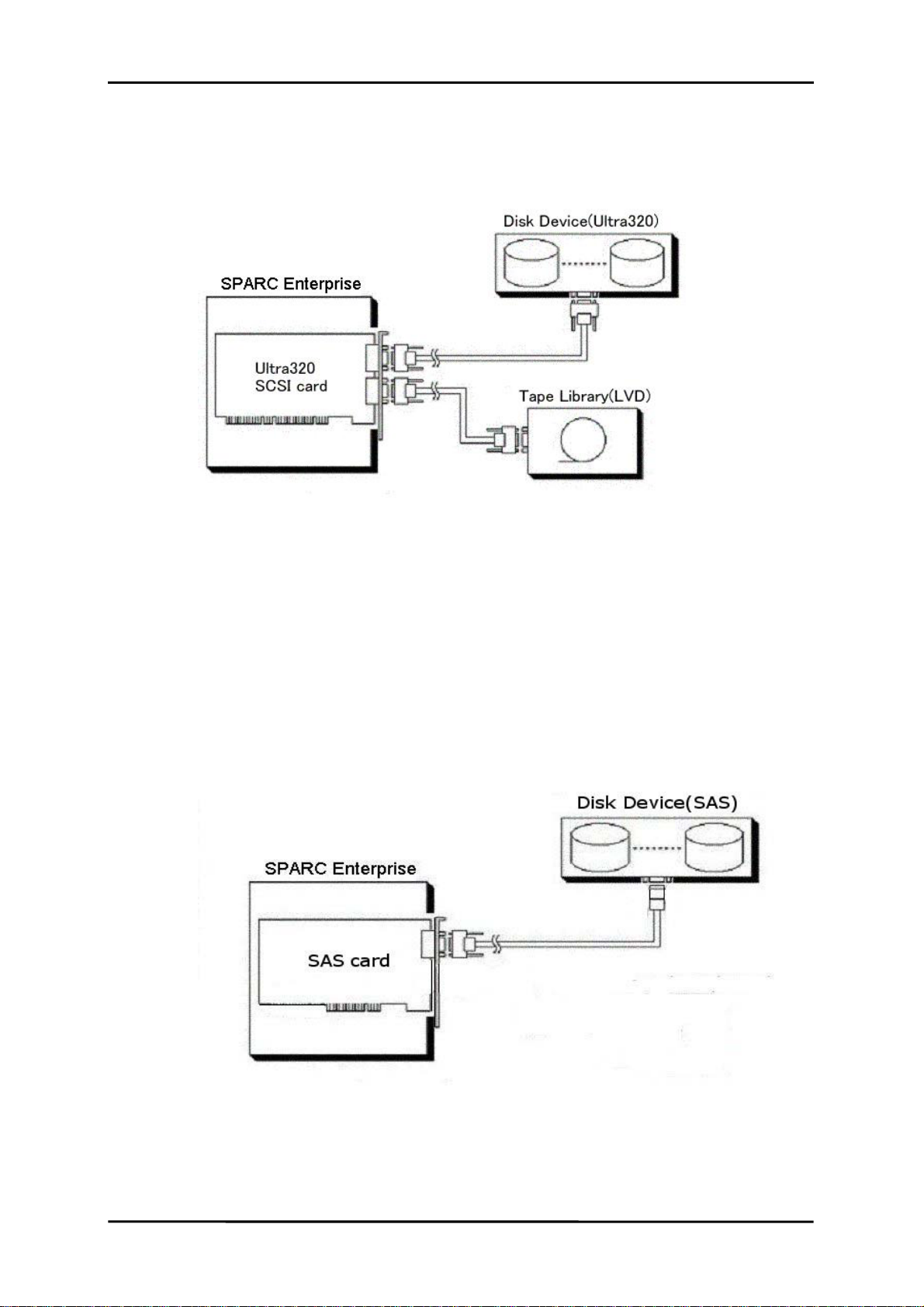
1.1 Function Overview
Fujitsu ULTRA LVD SCSI Host Bus Adapter Driver 3.0 is a SCSI/SAS host bus adapter (HBA)
driver
[Figure 1‑1 Form of SCSI connection]
[Figure 1‑2 Form of SAS connection]
2
Page 8
1.2 Hardware Support
This section describes hardware supported by this software.
1.2.1 Ultra320 SCSI card (SE0X7SC1X, SE0X7SC2X)
To use this adapter, it must be installed in a PCI‑X/PCI‑Express slot in a server. The
adapter has two VHDCI ports for connections to LVD devices.
1.2.1.1 Specifications
Specifications for the adapter are given below.
[Table 11 Ultra320 SCSI specifications]
Interface port Ultra 320 SCSI
SCSI bus width 8 bits or 16 bits
Electrical interface Low voltage differential
Connector type VHDCI 68‑pin
Transfer rate Async mode: Maximum 7MB/s(per SCSI port)
Sync mode: Maximum: 320 MB/s (per SCSI
port)
Chapter 1 Overview
Maximum Cable Length 12m
Number of SCSI devices Up to 14 (per SCSI port)
Multi‑Initiator Support
Number of Initiator Maximum:2(per SCSI port)
[Table 12 PCI‑X bus specifications]
Specification compliance PCI‑X 1.0
Bus width 64 bit
Operating clock 133 MHz
Card form Low profile, MD2
Bracket form Standard Bracket
[Table 13 PCI Express specification]
Specification compliance PCI Express
Line speed 2.5Gbps
Number of lane x4
Card form Low profile, MD2
Bracket form Standard Bracket
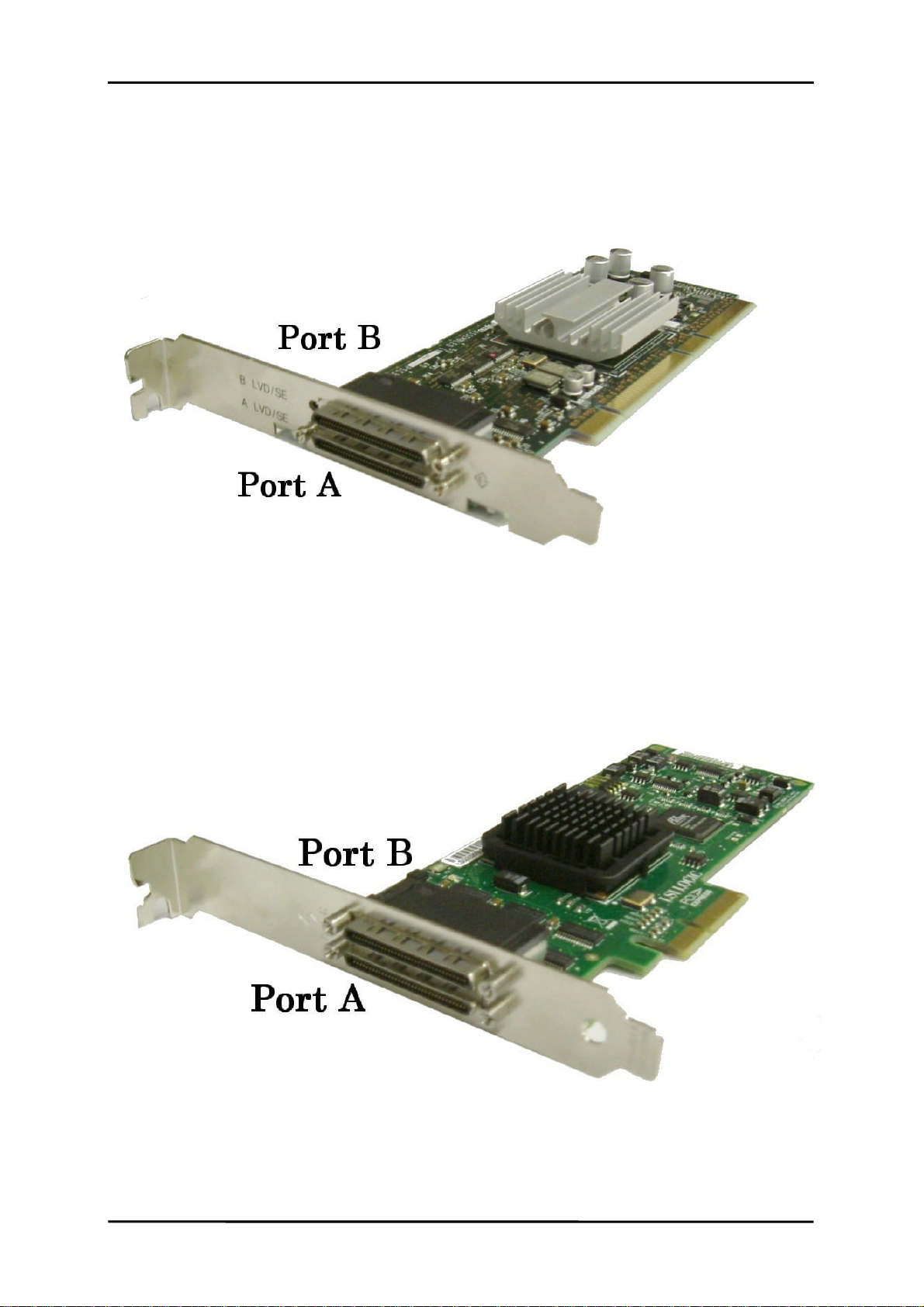
1.2.1.2 Physical description
Figure 13 and Figure 14 show the top of the Ultra320 SCSI cards. The different parts
together with their features are described below.
3
Page 9
Chapter 1 Overview
Port A is a LVD SCSI VHDCI connector. FJSV,(e)ulsa@#indicates that it is a SCSI bus.
Port B is a LVD SCSI VHDCI connector. FJSV,(e)ulsa@#,1indicates that it is a SCSI bus.
(#is a variable representing the PCI slot location of this card.)
[Figure 13 Top view of the Ultra320 SCSI card (SE0X7SC1X)]
[Figure 14 Top view of the Ultra320 SCSI card (SE0X7SC2X)]
4
Page 10
1.2.2 SAS card (SE0X7SA1X)
To use this adapter, it must be installed in a PCI Express slot in a server. The adapter
has one SAS x4 port for connections to SAS devices.
1.2.2.1 Specifications
Specifications for the adapter are given below.
Interface port Serial Attached SCSI
Transfer rate Max 3.0 Gbps x 4
Medium Interface Specification compliance:SAS‑1.1 (3Gbps)
Maximum Cable Length Max 6 m
[Table 15 PCI Express specification]
Chapter 1 Overview
[Table 14 SAS specifications]
Connector:SAS x4 connector
Specification compliance PCI Express
Line speed 2.5Gbps
Number of lane x4
Card form Low profile, MD2
Bracket form Standard Bracket
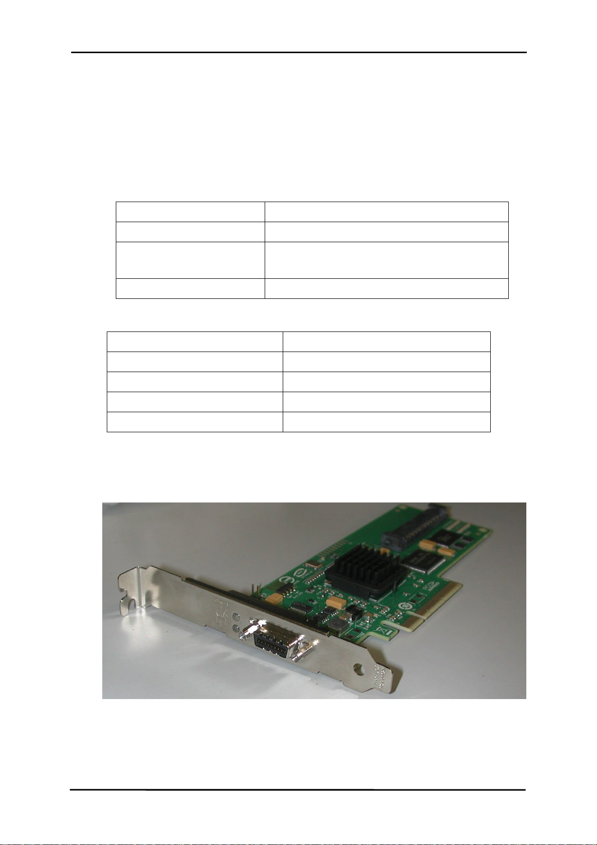
1.2.2.2 Physical description
Figure 15 show the top of the SAS cards. The different parts together with their features
are described below.
[Figure 15 Top view of the SAS card (SE0X7SA1X)]
5
Page 11

Chapter 2 Configuration
Chapter 2 Configuration
This chapter explains, the tasks required after installation of this software, so that
SCSI/SAS target driver can recognize devices. Explanations of tasks are given in the
following sequence:
Installing the driver
Configuring the driver software
Configuring I/O devices
6
Page 12

2.1 Installing the Driver
To use FUJITSU ULTRA LVD SCSI Host Bus Adapter Driver 3.0, install the package stored on
the SPARC Enterprise Software DVD. For the installation procedure, refer to the
Installation Guide – FUJITSU ULTRA LVD SCSI Host Bus Adapter Driver 3.0.
Chapter 2 Configuration
7
Page 13
Chapter 2 Configuration
2.2 Configuring the Driver Software
The section describes the settings required for the driver software.
2.2.1 disable‑u320 property setting
The disable‑u320 property setting must be configured as shown below in the fjulsa driver
definition file. Adding the following line to the /platform/{sun4v│SUNW,SPARC‑Enterprise}
/kernel/drv/fjulsa.conf file makes the disable‑u320 property effective:
disable‑u320=0x1:
2.2.2 Property setting for each port
When the properties in the fjulsa driver definition file (/platform/{sun4v│
SUNW,SPARC‑Enterprise}/kernel/drv/fjulsa.conf) are set according to explanations in
Section 2.2.1, the property setting are applied to each port of all Ultra320 SCSI/SAS cards
mounted in the server.
To make the properties valid only for a specific port of a specific SCSI/SAS card, define
the properties as follows:
name=drivername
parent=/pci@##,####
unit‑address=#
The name of the adapter driver corresponding to the SCSI/SAS card is defined in drivername
of the name property. Specify fjulsa for the Ultra320 SCSI/SAS card.
The parent node of the SCSI/SAS card as named in a device name is defined in /pci@##,####
of the parent property. For example, if a device name shows that the SCSI/SAS card port
is /pci@1d,4000/FJSV,(e)ulsa@3, specify /pci@1d,4000.
The device number of the SCSI/SAS card in the device name is specified for # of the
unit‑address property. For example, if a device name shows that the SCSI/SAS card port
is /pci@1d,4000/FJSV(e)ulsa@3, specify 3 immediately following
FJSV,(e)ulsa@.
In the following example, the disable‑u320 is set to 0x1 for the port of an Ultra320 SCSI/SAS
card indicated as /pci@1d,4000/FJSV,(e)ulsa@3in a device name:
name=fjulsa
parent=/pci@1d,4000
unit‑address=3
disable‑u320=0x1;
2.2.3 max‑throttle property setting
Some device such as disk drives can accept requests for multiple data transfers at the
same time. However, when the number of data transfer requests accepted by such a device
reaches the maximum number for the device, its queue becomes full, and the SCSI/SAS HBA
driver is notified of this status so that no more requests are sent from the driver.
Therefore, processing for data transfer requests is temporarily interrupted occasionally,
and data transfer efficiency decreases as a result.
The max‑throttle property of the fjulsa driver has been prepared as a means of preventing
this problem. By setting the max‑throttle property to a value below the maximum number
of data transfer requests that a device can handle concurrently, the number of data transfer
requests issued at the same time to the device is limited and a queue‑full state can be
8
Page 14

Chapter 2 Configuration
prevented.
Adding the following line to the /platform/{sun4v│SUNW,SPARC‑Enterprise}/kernel/drv/
fjulsa.conf file makes the max‑throttle property effective:
max‑throttle=##;
(##: Number of data transfer requests that can be issued at the same time)
Moreover, the target#‑max‑throttle property (# is SCSI ID) can be set to limit the number
of data transfer request issued to a device with a specific SCSI ID.
Adding the following line to the /platform/{sun4v│SUNW,SPARC‑Enterprise}/kernel/drv
/fjulsa.conf file makes the target#‑max‑throttle property effective:
target#‑max‑throttle=##;
(#:SCSI ID, ##: Number of data transfer requests which can be issued at the same time)
In the following example, the number of data transfer requests that can be issued at the
same time to a device with SCSI ID=1 is limited to 128:
target1‑max‑throttle=128;
For information on the maximum number of data transfer requests that a device can handle
concurrently, refer to the manual of the device.
For the changes in fjulsa.conf to take effect in the kernel, reboot the machine as follows
2.3.4 Reconfiguring the kernel.
9
Page 15

Chapter 2 Configuration
2.3 Configuring I/O devices
This section describes the tasks required to enable the SCSI/SAS target driver to identify
disk devices. In the explanation here, these tasks are discussed based on the assumption
that the sd driver (SCSI disk driver) is used.
Please refer to the manual of each device for the definition of the control driver of other
I/O devices such as tape drive.
2.3.1 Collecting information about the devices to be connected
First, collect the following information about the devices that will be connected:
SCSI target ID for each device
Logical unit (LU: Logical Unit) number included with each device
WWID of HBA (SAS)
Information on the device with which the server for the installation is connected by
executing "probe‑scsi‑all" on OBP can be confirmed.
{0} ok probe‑scsi‑all
/pci@7,700000/FJSV,eulsa@0
MPT Version : 01.05 , Firmware Version : 01.24.00.00
SAS World Wide ID(HBA:Port0) is 0x500605b0 003cf854
Target 0x1c
Unit 0x0 Disk FUJITSU E2000 0000 2097152 Blocks, 1073 MB
Unit 0x1 Disk FUJITSU E2000 0000 2097152 Blocks, 1073 MB
:
2.3.2 Editing the sd.conf
The definition file for the sd driver is /kernel/drv/sd.conf add the collected information
to this file. sd.conf contains several default settings.
#
# Copyright (c) 1992, by Sun Microsystems, Inc.
#
#ident @(#)sd.conf 1.8 93/05/03 SMI
name=sd class=scsi
target=0 lun=0;
name=sd class=scsi
target=1 lun=0;
:
:
10
A definition begins with name=sdand ends with a semicolon (;). target=X specifies a
SCSI target ID. lun=X specifies a logical unit number. A line starting with a number sign
Page 16

Chapter 2 Configuration
(#) is a comment line.
For example, if a disk device is configured with SCSI target ID 0 and has three logical
units from 0 to 2, edit sd.conf as follows:
Use target=0 lun=0 as is, since it is an applicable definition.
Copy the two lines containing target=0 lun=0 twice. In the copied lines, change one lun=0
to lun=1 and the other to lun=2.
#
# Copyright (c) 1992, by Sun Microsystems, Inc.
#
#ident @(#)sd.conf 1.8 93/05/03 SMI
name=sd class=scsi
target=0 lun=0;
name=sd class=scsi
target=0 lun=1;
name=sd class=scsi
target=0 lun=2;
name=sd class=scsi
target=1 lun=0;
:
:
The sd driver now has all the necessary definitions.
2.3.3 Editing the ses.conf (File Unit)
The definition file for the ses driver is /kernel/drv/ses.conf add the collected
information to this file. ses.conf contains several default settings.
A definition begins with name=sesand ends with a semicolon (;). target=X specifies
a SCSI target ID. lun=X specifies a logical unit number. A line starting with a number
sign (#) is a comment line.
For example, if the File Unit is configured with SES Controller target ID 32 and has one
logical unit 0, edit ses.conf as follows:
#
# Copyright 2003 Sun Microsystems, Inc. All rights reserved.
# Use is subject to license terms.
#
#
#ident "@(#)ses.conf 1.11 03/10/23 SMI"
#
name="ses" class="scsi" target=0 lun=0;
name="ses" class="scsi" target=1 lun=0;
name="ses" class="scsi" target=2 lun=0;
…
11
Page 17

Chapter 2 Configuration
name="ses" class="scsi" target=32 lun=0;
2.3.4 Reconfiguring the kernel
For the changes in sd.conf to take effect in the kernel, reboot the machine as follows:
# touch /reconfigure
# /usr/sbin/shutdown –i6 –g0 ‑y
The sd driver can now recognize the SCSI devices. Use the format command to check the
recognition results.
Next, write a disk label or define a partition with the formatting command as explained
in the manual for each device.
12
Page 18

2.4 Network Install
When you install the driver in the server connected to this SCSI/SAS card with an
installation server. Please refer to the following manual when the target machine of the
network installation is SPARC Enterprise.
・Install Server Build Guide I/O device driver (SPARC Enterprise)
Chapter 2 Configuration
13
Page 19

Chapter 3 Troubleshooting
Chapter 3 Troubleshooting
Check the following if a problem occurs.
14
Page 20

Chapter 3 Troubleshooting
■ Has the driver been installed?
Enter pkginfo –x FJSV,(e)ulsa and if nothing is displayed, the driver has not been installed.
Install the driver from the SPARC Enterprise Software DVD. For Ultra320 SCSI/SAS on a 32‑bit
kernel, install the FJSV,(e)ulsa package, and for a 64‑bit kernel, install the FJSV,(e)ulsa
packages; otherwise, the fjulsa driver does not operate property.
■ Does the SCSI device have a valid operating status and correct configuration?
If you cannot see the name of the device that you want to use, it may be off, its SCSI
ID or logical unit number may be wrong, the device configuration in the SCSI/SAS target
driver (such as in sd.conf) may be wrong, or device definitions are not yet valid in the
kernel. Check the status of the device, its configuration, and the SCSI/SAS target driver
configuration. Changes in a device configuration do not become valid until the device is
turned off and then on again. If a device is not correctly identified even though its
configuration is correct, turn the device off and then on again.
■ Does the SCSI bus have duplicate SCSI IDs?
If the Initiator ID and SCSI ID for a device are the same on a SCSI bus, correct SCSI bus
operation is not possible.
In this event, check the Initiator ID and SCSI ID of the device. Methods of identifying
the current Initiator ID are shown below.
Checking the OBP configuration
ok> printenv scsi‑initiator‑id
scsi‑initiator‑id= 7
ok>
Checking the /var/adm/messages file
1. Search for initiator SCSI ID now in the /var/adm/messages file.
2. If you find the following messages, the Initiator ID was changed from 7 to 6:
unix: /pci@##,####/FJSV,(e)ulsa@# (fjulsa#): (*1)
initiator SCSI ID now 6
*1:# is decimal number or hexadecimal number.
3. If you cannot find messages similar to the above messages, the Initiator ID is
7, which is the default Initiator ID.
If different IDs are found with the methods, the result of checking the messages file takes
priority.
The software and hardware requirements describe below must be met for use of this software.
15
Page 21

Appendix A Messages
Appendix A Messages
16
Page 22

Appendix A Messages
A.1 Warning messages
WARNING: fjulsa#: Device is using a hilevel intr
Hilevel interrupt handler was specified to be the fjulsa driver. Installed memory may be insufficient. If the amount of
memory does not seem to be the problem, contact a support representative.
WARNING: fjulsa#: cannot allocate soft state
Acquisition of a control domain went wrong into attach of the fjulsa driver. Installed memory may be insufficient. If the
amount of memory does not seem to be the problem, contact a support representative.
WARNING: fjulsa#: cannot get soft state
Acquisition of state information went wrong into attach of the fjulsa driver. Installed memory may be insufficient. If the
amount of memory does not seem to be the problem, contact a support representative.
WARNING:/pci@#,#/FJSV,(e)ulsa@#(fjulsa#):
ulsa_config_space_init failed
Initialization of PCI configuration register went wrong into attach of the fjulsa driver. Please refer to the following columns.
WARNING:/pci@#,#/FJSV,(e)ulsa@#(fjulsa#):
cannot map configuration space
WARNING:/pci@#,#/FJSV,(e)ulsa@#(fjulsa#):
not supported vendor ID (#)
WARNING:/pci@#,#/FJSV,(e)ulsa@#(fjulsa#):
LSILogic PCI device (1000,#) not supported
WARNING:/pci@#,#/FJSV,(e)ulsa@#(fjulsa#):
map setup failed
An operating register could not be mapped while the fjulsa driver was being attached. Installed memory may be insufficient.
If the amount of memory does not seem to be the problem, contact a support representative.
WARNING:/pci@#,#/FJSV,(e)ulsa@#(fjulsa#):
get iblock cookie failed
An area for registering an interrupt handler could not be allocated while the fjulsa driver was being attached. Installed
memory may be insufficient. If the amount of memory does not seemto be the problem, contact a support representative.
17
Page 23

Appendix A Messages
WARNING:/pci@#,#/FJSV,(e)ulsa@#(fjulsa#):
adding interrupt failed
An interrupt handler could not be registered while the fjulsa driver was being attached. Installed memory may be insufficient.
If the amount of memory does not seem to be the problem, contact a support representative.
WARNING:/pci@#,#/FJSV,(e)ulsa@#(fjulsa#):
hba attach setup failed
hba attach could not be set up while the fjulsa driver was being attached. Installed memory may be insufficient. If the
amount of memory does not seem to be the problem, contact a support representative.
WARNING:/pci@#,#/FJSV,(e)ulsa@#(fjulsa#):
creating kmem cache failed
A control area could not be allocated while the fjulsa driver was being attached. Installed memory may be insufficient. If the
amount of memory does not seem to be the problem, contact a support representative.
WARNING:/pci@#,#/FJSV,(e)ulsa@#(fjulsa#):
creating minor node failed
Control information could not be created while the fjulsa driver was being attached. Installed memory may be insufficient. If
the amount of memory does not seem to be the problem, contact a support representative.
WARNING:/pci@#,#/FJSV,(e)ulsa@#(fjulsa#):
Target #: disabled TQ since disconnects are disabled
The TAG setting was invalidated because disconnect disabled is specified for target#. Contact customer support.
WARNING:/pci@#,#/FJSV,(e)ulsa@#(fjulsa#):
creating pm component failed
The pm component could not be created while the fjulsa driver was being attached. Installed memory may be insufficient. If
the amount of memory does not seem to be the problem, contact a support representative.
WARNING:/pci@#,#/FJSV,(e)ulsa@#(fjulsa#):
ulsa_hs_msg_init failed
An area for Handshake could not be allocated while the fjulsa driver was being attached. Installed memory may be
insufficient. If the amount of memory does not seem to be the problem, contact a support representative.
18
Page 24

Appendix A Messages
WARNING:/pci@#,#/FJSV,(e)ulsa@#(fjulsa#):
ulsa_memory_confpage_init failed
An area for configuration pages could not be allocated while the fjulsa driver was being attached. Installed memory may be
insufficient. If the amount of memory does not seem to be the problem, contact a support representative.
WARNING:/pci@#,#/FJSV,(e)ulsa@#(fjulsa#):
ulsa_memory_fw_init failed
An area for downloading firmware could not be allocated while the fjulsa driver was being attached. Installed memory may
be insufficient. If the amount of memory does not seem to be theproblem, contact a support representative.
WARNING:/pci@#,#/FJSV,(e)ulsa@#(fjulsa#):
ulsa_reply_msg_init failed
An area for reply messages could not be allocated while the fjulsa driver was being attached. Installed memory may be
insufficient. If the amount of memory does not seem to be the problem, contact a support representative.
WARNING:/pci@#,#/FJSV,(e)ulsa@#(fjulsa#):
ulsa_request_msg_init failed
An area for request messages could not be allocated while the fjulsa driver was being attached. Installed memory may be
insufficient. If the amount of memory does not seem to be the problem, contact a support representative.
WARNING:/pci@#,#/FJSV,(e)ulsa@#(fjulsa#):
attach failed
The fjulsa driver could not be attached. Take corrective action by following the instructions given in the message output
before this message.
WARNING:/pci@#,#/FJSV,(e)ulsa@#(fjulsa#):
cannot map configuration space.
The PCI configuration register of the fjulsa driver could not be mapped. Contact customer support.
WARNING:/pci@#,#/FJSV,(e)ulsa@#(fjulsa#):
not supported vendor ID (#)
A vendor ID not supported by the fjulsa driver was detected. Contact customer support.
WARNING:/pci@#,#/FJSV,(e)ulsa@#(fjulsa#):
LSILogic PCI device (1000,#) not supported.
The fjulsa driver could not control this adapter. Contact customer support.
19
Page 25

Appendix A Messages
WARNING:/pci@#,#/FJSV,(e)ulsa@#(fjulsa#):
Unable to allocate dma handle.
The dma area could not be allocated. Installed memory may be insufficient. If the amount of memory does not seem to be
the problem, contact a support representative.
WARNING:/pci@#,#/FJSV,(e)ulsa@#(fjulsa#):
Unable to allocate memory for dma.
The dma area could not be allocated. Installed memory may be insufficient. If the amount of memory does not seem to be
the problem, contact a support representative.
WARNING:/pci@#,#/FJSV,(e)ulsa@#(fjulsa#):
Unable to bind DMA resources.
The dma area could not be allocated. Installed memory may be insufficient. If the amount of memory does not seem to be
the problem, contact a support representative.
WARNING:/pci@#,#/FJSV,(e)ulsa@#(fjulsa#):
chip reset failed
Chip reset processing failed. Replace the adapter. Contact customer support.
WARNING:/pci@#,#/FJSV,(e)ulsa@#(fjulsa#):
IOC not come to READY state
The SCSI/SAS control chip could not be changed to the READY state after chip reset was completed. Contact customer
support.
WARNING:/pci@#,#/FJSV,(e)ulsa@#(fjulsa#):
IOC status changed: %s
The status of the SCSI control chip has changed.
%s="RESET" "FAULT"
When indicated by repetition, Contact customer support.
WARNING:/pci@#,#/FJSV,(e)ulsa@#(fjulsa#):
IOC status changed: ioc_stat = #
The status of the SCSI/SAS control chip cannot be determined. Contact customer support.
20
Page 26

WARNING:/pci@#,#/FJSV,(e)ulsa@#(fjulsa#):
Unexpected DMA state: PCI Parity Error. fault code = #
A DMA parity error occurred on the PCI bus. Contact customer support.
WARNING:/pci@#,#/FJSV,(e)ulsa@#(fjulsa#):
Unexpected DMA state: PCI Bus Fault. fault code = #
A bus error occurred on the PCI bus. Check the PCI bus status. Contact customer support.
WARNING:/pci@#,#/FJSV,(e)ulsa@#(fjulsa#):
No SMFA is in Reply Post FIFO: reply = #
A reply message interrupt was received without an interrupt source. Contact customer support.
WARNING:/pci@#,#/FJSV,(e)ulsa@#(fjulsa#):
invalid context reply: reply = #
Appendix A Messages
An invalid context reply was received. Contact customer support.
WARNING:/pci@#,#/FJSV,(e)ulsa@#(fjulsa#):
invalid address reply : addr = #
An invalid address reply was received. Contact customer support.
WARNING:/pci@#,#/FJSV,(e)ulsa@#(fjulsa#):
IOC received invalid SGL
The SCSI/SAS control chip received an invalid scatter-gather list. Contact customer support.
WARNING:/pci@#,#/FJSV,(e)ulsa@#(fjulsa#):
IOC is in invalid state
An internal error occurred in the SCSI/SAS control chip. Contact customer support.
WARNING:/pci@#,#/FJSV,(e)ulsa@#(fjulsa#):
IOC internal error occurred
An internal error occurred in the SCSI/SAS control chip. Contact customer support.
21
Page 27

Appendix A Messages
WARNING:/pci@#,#/FJSV,(e)ulsa@#(fjulsa#):
Resetting scsi bus, data overrun: got too much data from target (#,#)
A data overrun error was detected during target #,# control. The SCSI/SAS bus was reset. The SCSI/SAS unit and cable may
have a fault. Contact customer support.
WARNING:/pci@#,#/FJSV,(e)ulsa@#(fjulsa#):
SCSI bus parity error from target (%d,%d)
A SCSI/SAS bus parity error was detected during target #,# control. The SCSI/SAS unit and cable may have a fault. Contact
customer support.
WARNING:/pci@#,#/FJSV,(e)ulsa@#(fjulsa#):
Resetting scsi bus, protocol error occurred from target (#,#)
A protocol error was detected during target #,# control. The SCSI/SAS bus was reset. The SCSI/SAS unit and cable may
have a fault. Contact customer support.
WARNING:/pci@#,#/FJSV,(e)ulsa@#(fjulsa#):
invalid task termination interrupt
An invalid task termination interrupt was detected. Contact customer support.
WARNING:/pci@#,#/FJSV,(e)ulsa@#(fjulsa#):
Resetting scsi bus: IOC found SCSI bus error from target (#,#)
A SCSI/SAS bus error was detected during target #,# control. The SCSI/SAS bus was reset. The SCSI/SAS unit and cable
may have a fault. Contact customer support.
WARNING:/pci@#,#/FJSV,(e)ulsa@#(fjulsa#):
invalid count of terminated commands
The fjulsa driver's problem concerning SCSI/SAS bus reset processing. Contact customer support.
WARNING:/pci@#,#/FJSV,(e)ulsa@#(fjulsa#):
got unexpected EventNotification reply message
An unexpected EventNotification reply message was received. Contact customer support.
WARNING:/pci@#,#/FJSV,(e)ulsa@#(fjulsa#):
got unexpected EventAck reply message
An unexpected EventAck reply message was received. Contact customer support.
22
Page 28

Appendix A Messages
WARNING:/pci@#,#/FJSV,(e)ulsa@#(fjulsa#):
command timeout for Target #.#
The Target #,# command did not terminate after the specified time elapsed. The SCSI/SAS unit and cable may have a fault.
Contact customer support.
WARNING:/pci@#,#/FJSV,(e)ulsa@#(fjulsa#):
timeout on EventAck message interrupt
The EventAck message timed out. Contact customer support.
WARNING:/pci@#,#/FJSV,(e)ulsa@#(fjulsa#):
IOC is in fault status. doorbell = #
The SCSI/SAS control chip is faulty. When indicated by repetition, Contact customer support.
WARNING:/pci@#,#/FJSV,(e)ulsa@#(fjulsa#):
Reset History did not clear
The SCSI/SAS control chip history could not be cleared. Contact customer support.
WARNING:/pci@#,#/FJSV,(e)ulsa@#(fjulsa#):
Target # disabled wide SCSI mode
Wide SCSI transfer of the target# was invalidated. Contact customer support.
WARNING:/pci@#,#/FJSV,(e)ulsa@#(fjulsa#):
Target # reverting to async. Mode
The target# is transferred asynchronously. Contact customer support.
WARNING:/pci@#,#/FJSV,(e)ulsa@#(fjulsa#):
Target # reducing sync. transfer rate
The synchronous transfer rate of the target# has been reduced. Contact customer support.
WARNING: /pci@#,#/FJSV,(e)ulsa@# (fjulsa#):
Auto Request Sense emulation failed
Auto Request Sense failed because of the settings of the upper driver.
Contact customer support.
23
Page 29

Appendix A Messages
WARNING: /pci@#,#/FJSV,(e)ulsa@# (fjulsa#):
IOC message timeout occurred. IOC stat = #
An IOC message timeout occurred because an error of SCSI/SAS control chip is faulty. Contact customer support.
WARNING: /pci@#,#/FJSV,(e)ulsa@# (fjulsa#):
handshake busy retry out
The number of retries reached the upper limit when the busy status was detected during the handshake processing. Contact
customer support.
WARNING: /pci@#,#/FJSV,(e)ulsa@# (fjulsa#):
PCI Bus error occurred. status=#
An error occurred on the PCI bus. Contact customer support.
WARNING: /pci@#,#/FJSV,eulsa@# (fjulsa#):
first chip reset failed
First SCSI/SAS Control chip reset failed. Contact customer support.
WARNING: /pci@#,#/FJSV,eulsa@# (fjulsa#):
invalid base-wwid
SAS base-wwid invalid. Contact customer support.
WARNING: /pci@#,#/FJSV,eulsa@# (fjulsa#):
get base-wwid failed
SAS base-wwid failed. Contact customer support.
WARNING: /pci@#,#/FJSV,eulsa@# (fjulsa#):
too many device capabilities.
PCI Capabilities exceeds the upper bound. Contact customer support.
WARNING: /pci@#,#/FJSV,eulsa@# (fjulsa#):
capabilities pointer 0x%x out of range.
PCI Capabilities pointer out of range. Contact customer support.
24
Page 30

WARNING: /pci@#,#/FJSV,eulsa@# (fjulsa#):
PCI Express Capability not found.
PCI Express Capability not found. Contact customer support.
WARNING: /pci@#,#/FJSV,eulsa@# (fjulsa#):
MSI Capability not found.
Fjulsa driver is not support MSI. Contact customer support.
WARNING: /pci@#,#/FJSV,eulsa@# (fjulsa#):
timeout on EventAck message interrupt.
An EventAck message interrupt timeout occurred because an error of SAS control chip is faulty.
Contact customer support.
Appendix A Messages
WARNING: /pci@#,#/FJSV,eulsa@# (fjulsa#):
timeout on SAS IO Unit Control message interrupt.
An SAS IO Unit Control message interrupt timeout occurred because an error of SAS control chip is faulty.
Contact customer support.
WARNING: /pci@#,#/FJSV,eulsa@# (fjulsa#):
getting interrupt type failed.
Getting interrupt type failed. Contact customer support.
WARNING: /pci@#,#/FJSV,eulsa@# (fjulsa#):
MSI interrupt is unsupported
Fjulsa driver is not support MSI. Contact customer support.
WARNING: /pci@#,#/FJSV,eulsa@# (fjulsa#):
getting number of interrupt failed
Getting interrupt resource failed. Contact customer support.
WARNING: /pci@#,#/FJSV,eulsa@# (fjulsa#):
getting number of available interrupts failed
Getting interrupt resource failed. Contact customer support.
25
Page 31

Appendix A Messages
WARNING: /pci@#,#/FJSV,eulsa@# (fjulsa#):
allocating internal control area failed
Getting interrupt resource failed. Contact customer support.
WARNING: /pci@#,#/FJSV,eulsa@# (fjulsa#):
getting interrupt priority failed
Getting interrupt resource failed. Contact customer support.
WARNING: /pci@#,#/FJSV,eulsa@# (fjulsa#):
adding interrupt handler failed
Adding interrupt handler failed. Contact customer support.
26
Page 32

Appendix A Messages
A.2 PANIC messages
PANIC:/pci@#,#/FJSV,(e)ulsa@#(fjulsa#):
Not in softc list!
An internal consistency error was detected while the fjulsa# driver was being detached. Contact customer support.
PANIC:/pci@#,#/FJSV,(e)ulsa@#(fjulsa#):
ulsa_pkt_destroy_extern: freeing free packet
A release request was issued for the pkt structure area that has already been reallocated. Upper driver is faulty. Contact
customer support.
PANIC:/pci@#,#/FJSV,(e)ulsa@#(fjulsa#):
timeout on bus reset interrupt
A timeout occurred during a bus reset interrupt. . The SCSI unit and cable may have a fault. Contact customer support.
PANIC:/pci@#,#/FJSV,(e)ulsa@#(fjulsa#):
invalid queue entry cmd=#
The fjulsa driver's internal contradiction was detected. Contact customer support.
PANIC:/pci@#,#/FJSV,(e)ulsa@#(fjulsa#):
ulsa_waitq_delete: queue botch
The fjulsa driver's internal contradiction was detected. Contact customer support.
27
Page 33

Appendix A Messages
A.3 Information messages
/pci@#,#/FJSV,(e)ulsa@#(fjulsa#):
scsi reset delay of 0 is not recommended, resetting to SCSI_DEFAULT_RESET_DELAY
Because 0 is specified for the scsi-reset-delay property, the default value is restored. Review the settings in the fjulsa.conf
file.
/pci@#,#/FJSV,(e)ulsa@#(fjulsa#):
transfer rate and width for Target (#,#) was set up.
transfer rate = %s, width = %ss
The transfer rate was changed.
%s="#ns" "async"
%ss="Wide" "Narrow"
Confirm whether the SCSI device supports the synchronous transfer mode and wide transfer mode if %s is "Async" and %ss
is "Narrow". When either mode is not supported, no problem occurred. When either mode is supported, contact customer
support.
/pci@#,#/FJSV,(e)ulsa@#(fjulsa#):
ulsa_hbaq_delete: target #- was on hbaq # times.
More than one logical unit is registered with hbaq. No problem occurred.
/pci@#,#/FJSV,(e)ulsa@#(fjulsa#):
function # done, IOCStatus = #, IOCLogInfo = #
Unexpected status was notified from SCSI control chip.
/pci@#,#/FJSV,(e)ulsa@# (fjulsa#):
target#-scsi-options=#
A value of the target#-scsi-options property was specified.
No problem occurred.
/pci@#,#/FJSV,(e)ulsa@# (fjulsa#):
loginfo = #
The loginfo information was reported from the SCSI control chip.
If a WARNING message has been output before this message, follow the instructions given in the WARNING message.
28
Page 34

/pci@#,#/FJSV,(e)ulsa@# (fjulsa#):
Cmd (#) dump for Target # Lun #:
Information regarding timeout
Follow the instructions given in the following message.
WARNING: /pci@#,#/FJSV,(e)ulsa@# (fjulsa#):
IOC message timeout occurred. IOC stat = #
WARNING: /pci@#,#/FJSV,(e)ulsa@# (fjulsa#):
command timeout for Target #.#
WARNING: /pci@#,#/FJSV,(e)ulsa@# (fjulsa#):
timeout on EventAck message interrupt
/pci@#,#/FJSV,(e)ulsa@# (fjulsa#):
cdb=[ # # # # # # ]
Information regarding timeout
Follow the instructions given in the following message.
WARNING: /pci@#,#/FJSV,(e)ulsa@# (fjulsa#):
IOC message timeout occurred. IOC stat = #
WARNING: /pci@#,#/FJSV,(e)ulsa@# (fjulsa#):
command timeout for Target #.#
WARNING: /pci@#,#/FJSV,(e)ulsa@# (fjulsa#):
timeout on EventAck message interrupt
Appendix A Messages
/pci@#,#/FJSV,(e)ulsa@# (fjulsa#):
pkt_flags=# pkt_statistics=# pkt_state=#
Information regarding timeout
Follow the instructions given in the following message.
WARNING: /pci@#,#/FJSV,(e)ulsa@# (fjulsa#):
IOC message timeout occurred. IOC stat = #
WARNING: /pci@#,#/FJSV,(e)ulsa@# (fjulsa#):
command timeout for Target #.#
WARNING: /pci@#,#/FJSV,(e)ulsa@# (fjulsa#):
timeout on EventAck message interrupt
/pci@#,#/FJSV,(e)ulsa@# (fjulsa#):
pkt_scbp=# cmd_flags=#
Information regarding timeout
Follow the instructions given in the following message.
WARNING: /pci@#,#/FJSV,(e)ulsa@# (fjulsa#):
IOC message timeout occurred. IOC stat = #
WARNING: /pci@#,#/FJSV,(e)ulsa@# (fjulsa#):
command timeout for Target #.#
29
Page 35

Appendix A Messages
WARNING: /pci@#,#/FJSV,(e)ulsa@# (fjulsa#):
timeout on EventAck message interrupt
/pci@#,#/FJSV,(e)ulsa@#(fjulsa#):
LSILogic LSI53C1030 found.
The supported SCSI card was detected. No problem occurred.
fjulsa# is /pci@#,#/FJSV,(e)ulsa@#
The fjulsa driver was attached. No problem occurred.
/pci@#,#/FJSV,(e)ulsa@#(fjulsa#):
LSILogic LSISAS1068E found.
The supported SAS card was detected. No problem occurred.
/pci@#,#/FJSV,(e)ulsa@# (fjulsa#):
fjulsa#: Initiator WWNs: 0x#-0x#
WWN of the SAS card is displayed. No problem occurred.
30
Page 36

Appendix B PCI Slot Number and Device Name
Appendix B PCI Slot Number and Device Name
The appendix provides the PCI slot number and device name matrix for the following
SUNW,SPARC‑Enterprise models.
SPARC Enterprise M4000/M5000
SPARC Enterprise M8000/M9000
31
Page 37

Appendix B PCI Slot Number and Device Name
SPARC Enterprise M4000/M5000
Board Number Slot Number Device Name
Logical
System
Board
#0
Slot
PCI#1
IOBoat(X)
PCI#1
IOBoat(Ex)
Basic PCI
Slot
PCI#2
IOBoat(X)
PCI#2
IOBoat(Ex)
Basic PCI
Slot
PCI#3
IOBoat(X)
PCI#3
IOBoat(Ex)
Basic PCI
Slot
PCI#4 PCI#4‑PCIX1 /pci@3,700000/pci@0/pci@1/pci@0/****@4
PCI#0 /pci@0,600000/pci@0/pci@8/pci@0,1/****@1Basic PCI
PCI#1 /pci@0,600000/pci@0/pci@9/****@0
PCI#1‑PCIX1 /pci@0,600000/pci@0/pci@9/pci@0/pci@1/pci@0/****@4
PCI#1‑PCIX2 /pci@0,600000/pci@0/pci@9/pci@0/pci@1/pci@0,1/****@4
PCI#1‑PCIX5 /pci@0,600000/pci@0/pci@9/pci@0/pci@8/pci@0/****@4
PCI#1‑PCIX6 /pci@0,600000/pci@0/pci@9/pci@0/pci@8/pci@0,1/****@4
PCI#1‑PCIX3 /pci@0,600000/pci@0/pci@9/pci@0/pci@9/pci@0/****@4
PCI#1‑PCIX4 /pci@0,600000/pci@0/pci@9/pci@0/pci@9/pci@0,1/****@4
PCI#1‑PCIE1 /pci@0,600000/pci@0/pci@9/pci@0/pci@1/pci@0/pci@0/****@0
PCI#1‑PCIE2 /pci@0,600000/pci@0/pci@9/pci@0/pci@1/pci@0/pci@1/****@0
PCI#1‑PCIE3 /pci@0,600000/pci@0/pci@9/pci@0/pci@1/pci@0/pci@9/****@0
PCI#1‑PCIE4 /pci@0,600000/pci@0/pci@9/pci@0/pci@9/pci@0/pci@0/****@0
PCI#1‑PCIE5 /pci@0,600000/pci@0/pci@9/pci@0/pci@9/pci@0/pci@1/****@0
PCI#1‑PCIE6 /pci@0,600000/pci@0/pci@9/pci@0/pci@9/pci@0/pci@9/****@0
PCI#2 /pci@1,700000/****@0
PCI#2‑PCIX1 /pci@1,700000/pci@0/pci@1/pci@0/****@4
PCI#2‑PCIX2 /pci@1,700000/pci@0/pci@1/pci@0,1/****@4
PCI#2‑PCIX5 /pci@1,700000/pci@0/pci@8/pci@0/****@4
PCI#2‑PCIX6 /pci@1,700000/pci@0/pci@8/pci@0,1/****@4
PCI#2‑PCIX3 /pci@1,700000/pci@0/pci@9/pci@0/****@4
PCI#2‑PCIX4 /pci@1,700000/pci@0/pci@9/pci@0,1/****@4
PCI#2‑PCIE1 /pci@1,700000/pci@0/pci@1/pci@0/pci@0/****@0
PCI#2‑PCIE2 /pci@1,700000/pci@0/pci@1/pci@0/pci@1/****@0
PCI#2‑PCIE3 /pci@1,700000/pci@0/pci@1/pci@0/pci@9/****@0
PCI#2‑PCIE4 /pci@1,700000/pci@0/pci@9/pci@0/pci@0/****@0
PCI#2‑PCIE5 /pci@1,700000/pci@0/pci@9/pci@0/pci@1/****@0
PCI#2‑PCIE6 /pci@1,700000/pci@0/pci@9/pci@0/pci@9/****@0
PCI#3 /pci@2,600000/****@0
PCI#3‑PCIX1 /pci@2,600000/pci@0/pci@1/pci@0/****@4
PCI#3‑PCIX2 /pci@2,600000/pci@0/pci@1/pci@0,1/****@4
PCI#3‑PCIX5 /pci@2,600000/pci@0/pci@8/pci@0/****@4
PCI#3‑PCIX6 /pci@2,600000/pci@0/pci@8/pci@0,1/****@4
PCI#3‑PCIX3 /pci@2,600000/pci@0/pci@9/pci@0/****@4
PCI#3‑PCIX4 /pci@2,600000/pci@0/pci@9/pci@0,1/****@4
PCI#3‑PCIE1 /pci@2,600000/pci@0/pci@1/pci@0/pci@0/****@0
PCI#3‑PCIE2 /pci@2,600000/pci@0/pci@1/pci@0/pci@1/****@0
PCI#3‑PCIE3 /pci@2,600000/pci@0/pci@1/pci@0/pci@9/****@0
PCI#3‑PCIE4 /pci@2,600000/pci@0/pci@9/pci@0/pci@0/****@0
PCI#3‑PCIE5 /pci@2,600000/pci@0/pci@9/pci@0/pci@1/****@0
PCI#3‑PCIE6 /pci@2,600000/pci@0/pci@9/pci@0/pci@9/****@0
PCI#4 /pci@3,700000/****@0
32
Page 38

Appendix B PCI Slot Number and Device Name
Board Number Slot Number Device Name
PCI#4‑PCIX2 /pci@3,700000/pci@0/pci@1/pci@0,1/****@4
PCI#4‑PCIX5 /pci@3,700000/pci@0/pci@8/pci@0/****@4
PCI#4‑PCIX6 /pci@3,700000/pci@0/pci@8/pci@0,1/****@4
PCI#4‑PCIX3 /pci@3,700000/pci@0/pci@9/pci@0/****@4
PCI#4‑PCIX4 /pci@3,700000/pci@0/pci@9/pci@0,1/****@4
PCI#4‑PCIE1 /pci@3,700000/pci@0/pci@1/pci@0/pci@0/****@0
PCI#4‑PCIE2 /pci@3,700000/pci@0/pci@1/pci@0/pci@1/****@0
PCI#4‑PCIE3 /pci@3,700000/pci@0/pci@1/pci@0/pci@9/****@0
PCI#4‑PCIE4 /pci@3,700000/pci@0/pci@9/pci@0/pci@0/****@0
PCI#4‑PCIE5 /pci@3,700000/pci@0/pci@9/pci@0/pci@1/****@0
PCI#4‑PCIE6 /pci@3,700000/pci@0/pci@9/pci@0/pci@9/****@0
PCI#0 /pci@10,600000/pci@0/pci@8/pci@0,1/****@1Basic PCI
PCI#1 /pci@10,600000/pci@0/pci@9/****@0
PCI#1‑PCIX1 /pci@10,600000/pci@0/pci@9/pci@0/pci@1/pci@0/****@4
PCI#1‑PCIX2 /pci@10,600000/pci@0/pci@9/pci@0/pci@1/pci@0,1/****@4
PCI#1‑PCIX5 /pci@10,600000/pci@0/pci@9/pci@0/pci@8/pci@0/****@4
PCI#1‑PCIX6 /pci@10,600000/pci@0/pci@9/pci@0/pci@8/pci@0,1/****@4
PCI#1‑PCIX3 /pci@10,600000/pci@0/pci@9/pci@0/pci@9/pci@0/****@4
PCI#1‑PCIX4 /pci@10,600000/pci@0/pci@9/pci@0/pci@9/pci@0,1/****@4
PCI#1‑PCIE1 /pci@10,600000/pci@0/pci@9/pci@0/pci@1/pci@0/pci@0/****@0
PCI#1‑PCIE2 /pci@10,600000/pci@0/pci@9/pci@0/pci@1/pci@0/pci@1/****@0
PCI#1‑PCIE3 /pci@10,600000/pci@0/pci@9/pci@0/pci@1/pci@0/pci@9/****@0
PCI#1‑PCIE4 /pci@10,600000/pci@0/pci@9/pci@0/pci@9/pci@0/pci@0/****@0
PCI#1‑PCIE5 /pci@10,600000/pci@0/pci@9/pci@0/pci@9/pci@0/pci@1/****@0
PCI#1‑PCIE6 /pci@10,600000/pci@0/pci@9/pci@0/pci@9/pci@0/pci@9/****@0
PCI#2 /pci@11,700000/****@0
PCI#2‑PCIX1 /pci@11,700000/pci@0/pci@1/pci@0/****@4
PCI#2‑PCIX2 /pci@11,700000/pci@0/pci@1/pci@0,1/****@4
PCI#2‑PCIX5 /pci@11,700000/pci@0/pci@8/pci@0/****@4
PCI#2‑PCIX6 /pci@11,700000/pci@0/pci@8/pci@0,1/****@4
PCI#2‑PCIX3 /pci@11,700000/pci@0/pci@9/pci@0/****@4
PCI#2‑PCIX4 /pci@11,700000/pci@0/pci@9/pci@0,1/****@4
PCI#2‑PCIE1 /pci@11,700000/pci@0/pci@1/pci@0/pci@0/****@0
PCI#2‑PCIE2 /pci@11,700000/pci@0/pci@1/pci@0/pci@1/****@0
PCI#2‑PCIE3 /pci@11,700000/pci@0/pci@1/pci@0/pci@9/****@0
PCI#2‑PCIE4 /pci@11,700000/pci@0/pci@9/pci@0/pci@0/****@0
PCI#2‑PCIE5 /pci@11,700000/pci@0/pci@9/pci@0/pci@1/****@0
PCI#2‑PCIE6 /pci@11,700000/pci@0/pci@9/pci@0/pci@9/****@0
PCI#3 /pci@12,600000/****@0
PCI#3‑PCIX1 /pci@12,600000/pci@0/pci@1/pci@0/****@4
PCI#3‑PCIX2 /pci@12,600000/pci@0/pci@1/pci@0,1/****@4
PCI#3‑PCIX5 /pci@12,600000/pci@0/pci@8/pci@0/****@4
PCI#3‑PCIX6 /pci@12,600000/pci@0/pci@8/pci@0,1/****@4
PCI#3‑PCIX3 /pci@12,600000/pci@0/pci@9/pci@0/****@4
PCI#3‑PCIX4 /pci@12,600000/pci@0/pci@9/pci@0,1/****@4
PCI#3‑PCIE1 /pci@12,600000/pci@0/pci@1/pci@0/pci@0/****@0
PCI#3‑PCIE2 /pci@12,600000/pci@0/pci@1/pci@0/pci@1/****@0
Logical
System
Board
#1
IOBoat(X)
PCI#4
IOBoat(Ex)
Slot
PCI#1
IOBoat(X)
PCI#1
IOBoat(Ex)
Basic PCI
Slot
PCI#2
IOBoat(X)
PCI#2
IOBoat(Ex)
Basic PCI
Slot
PCI#3
IOBoat(X)
PCI#3
IOBoat(Ex)
33
Page 39

Appendix B PCI Slot Number and Device Name
Board Number Slot Number Device Name
PCI#3‑PCIE3 /pci@12,600000/pci@0/pci@1/pci@0/pci@9/****@0
PCI#3‑PCIE4 /pci@12,600000/pci@0/pci@9/pci@0/pci@0/****@0
PCI#3‑PCIE5 /pci@12,600000/pci@0/pci@9/pci@0/pci@1/****@0
PCI#3‑PCIE6 /pci@12,600000/pci@0/pci@9/pci@0/pci@9/****@0
Basic PCI
Slot
PCI#4
IOBoat(X)
PCI#4
IOBoat(Ex)
PCI#4 /pci@13,700000/****@0
PCI#4‑PCIX1 /pci@13,700000/pci@0/pci@1/pci@0/****@4
PCI#4‑PCIX2 /pci@13,700000/pci@0/pci@1/pci@0,1/****@4
PCI#4‑PCIX5 /pci@13,700000/pci@0/pci@8/pci@0/****@4
PCI#4‑PCIX6 /pci@13,700000/pci@0/pci@8/pci@0,1/****@4
PCI#4‑PCIX3 /pci@13,700000/pci@0/pci@9/pci@0/****@4
PCI#4‑PCIX4 /pci@13,700000/pci@0/pci@9/pci@0,1/****@4
PCI#4‑PCIE1 /pci@13,700000/pci@0/pci@1/pci@0/pci@0/****@0
PCI#4‑PCIE2 /pci@13,700000/pci@0/pci@1/pci@0/pci@1/****@0
PCI#4‑PCIE3 /pci@13,700000/pci@0/pci@1/pci@0/pci@9/****@0
PCI#4‑PCIE4 /pci@13,700000/pci@0/pci@9/pci@0/pci@0/****@0
PCI#4‑PCIE5 /pci@13,700000/pci@0/pci@9/pci@0/pci@1/****@0
PCI#4‑PCIE6 /pci@13,700000/pci@0/pci@9/pci@0/pci@9/****@0
SPARC Enterprise M8000/M9000
Board Number Slot Number Device Name
Logical
System
Board
#0
Basic PCI
Slot
Basic PCI
Slot
PCI#1
IOBoat(X)
PCI#1
IOBoat(Ex)
Basic PCI
Slot
Basic PCI
Slot
PCI#3
IOBoat(X)
PCI#3
IOBoat(Ex)
PCI#0 /pci@0,600000/****@0
PCI#1 /pci@1,700000/****@0
PCI#1‑PCIX1 /pci@1,700000/pci@0/pci@1/pci@0/****@4
PCI#1‑PCIX2 /pci@1,700000/pci@0/pci@1/pci@0,1/****@4
PCI#1‑PCIX5 /pci@1,700000/pci@0/pci@8/pci@0/****@4
PCI#1‑PCIX6 /pci@1,700000/pci@0/pci@8/pci@0,1/****@4
PCI#1‑PCIX3 /pci@1,700000/pci@0/pci@9/pci@0/****@4
PCI#1‑PCIX4 /pci@1,700000/pci@0/pci@9/pci@0,1/****@4
PCI#1‑PCIE1 /pci@1,700000/pci@0/pci@1/pci@0/pci@0/****@0
PCI#1‑PCIE2 /pci@1,700000/pci@0/pci@1/pci@0/pci@1/****@0
PCI#1‑PCIE3 /pci@1,700000/pci@0/pci@1/pci@0/pci@9/****@0
PCI#1‑PCIE4 /pci@1,700000/pci@0/pci@9/pci@0/pci@0/****@0
PCI#1‑PCIE5 /pci@1,700000/pci@0/pci@9/pci@0/pci@1/****@0
PCI#1‑PCIE6 /pci@1,700000/pci@0/pci@9/pci@0/pci@9/****@0
PCI#2 /pci@2,600000/****@0
PCI#3 /pci@3,700000/****@0
PCI#3‑PCIX1 /pci@3,700000/pci@0/pci@1/pci@0/****@4
PCI#3‑PCIX2 /pci@3,700000/pci@0/pci@1/pci@0,1/****@4
PCI#3‑PCIX5 /pci@3,700000/pci@0/pci@8/pci@0/****@4
PCI#3‑PCIX6 /pci@3,700000/pci@0/pci@8/pci@0,1/****@4
PCI#3‑PCIX3 /pci@3,700000/pci@0/pci@9/pci@0/****@4
PCI#3‑PCIX4 /pci@3,700000/pci@0/pci@9/pci@0,1/****@4
PCI#3‑PCIE1 /pci@3,700000/pci@0/pci@1/pci@0/pci@0/****@0
PCI#3‑PCIE2 /pci@3,700000/pci@0/pci@1/pci@0/pci@1/****@0
34
Page 40

Appendix B PCI Slot Number and Device Name
Board Number Slot Number Device Name
PCI#3‑PCIE3 /pci@3,700000/pci@0/pci@1/pci@0/pci@9/****@0
PCI#3‑PCIE4 /pci@3,700000/pci@0/pci@9/pci@0/pci@0/****@0
PCI#3‑PCIE5 /pci@3,700000/pci@0/pci@9/pci@0/pci@1/****@0
PCI#3‑PCIE6 /pci@3,700000/pci@0/pci@9/pci@0/pci@9/****@0
Logical
System
Board
#1
Basic PCI
Slot
Basic PCI
Slot
PCI#5
IOBoat(X)
PCI#5
IOBoat(Ex)
Basic PCI
Slot
Basic PCI
Slot
PCI#7
IOBoat(X)
PCI#7
IOBoat(Ex)
Basic PCI
Slot
Basic PCI
Slot
PCI#1
IOBoat(X)
PCI#1
IOBoat(Ex)
PCI#4 /pci@4,600000/****@0
PCI#5 /pci@5,700000/****@0
PCI#5‑PCIX1 /pci@5,700000/pci@0/pci@1/pci@0/****@4
PCI#5‑PCIX2 /pci@5,700000/pci@0/pci@1/pci@0,1/****@4
PCI#5‑PCIX5 /pci@5,700000/pci@0/pci@8/pci@0/****@4
PCI#5‑PCIX6 /pci@5,700000/pci@0/pci@8/pci@0,1/****@4
PCI#5‑PCIX3 /pci@5,700000/pci@0/pci@9/pci@0/****@4
PCI#5‑PCIX4 /pci@5,700000/pci@0/pci@9/pci@0,1/****@4
PCI#5‑PCIE1 /pci@5,700000/pci@0/pci@1/pci@0/pci@0/****@0
PCI#5‑PCIE2 /pci@5,700000/pci@0/pci@1/pci@0/pci@1/****@0
PCI#5‑PCIE3 /pci@5,700000/pci@0/pci@1/pci@0/pci@9/****@0
PCI#5‑PCIE4 /pci@5,700000/pci@0/pci@9/pci@0/pci@0/****@0
PCI#5‑PCIE5 /pci@5,700000/pci@0/pci@9/pci@0/pci@1/****@0
PCI#5‑PCIE6 /pci@5,700000/pci@0/pci@9/pci@0/pci@9/****@0
PCI#6 /pci@6,600000/****@0
PCI#7 /pci@7,700000/****@0
PCI#7‑PCIX1 /pci@7,700000/pci@0/pci@1/pci@0/****@4
PCI#7‑PCIX2 /pci@7,700000/pci@0/pci@1/pci@0,1/****@4
PCI#7‑PCIX5 /pci@7,700000/pci@0/pci@8/pci@0/****@4
PCI#7‑PCIX6 /pci@7,700000/pci@0/pci@8/pci@0,1/****@4
PCI#7‑PCIX3 /pci@7,700000/pci@0/pci@9/pci@0/****@4
PCI#7‑PCIX4 /pci@7,700000/pci@0/pci@9/pci@0,1/****@4
PCI#7‑PCIE1 /pci@7,700000/pci@0/pci@1/pci@0/pci@0/****@0
PCI#7‑PCIE2 /pci@7,700000/pci@0/pci@1/pci@0/pci@1/****@0
PCI#7‑PCIE3 /pci@7,700000/pci@0/pci@1/pci@0/pci@9/****@0
PCI#7‑PCIE4 /pci@7,700000/pci@0/pci@9/pci@0/pci@0/****@0
PCI#7‑PCIE5 /pci@7,700000/pci@0/pci@9/pci@0/pci@1/****@0
PCI#7‑PCIE6 /pci@7,700000/pci@0/pci@9/pci@0/pci@9/****@0
PCI#0 /pci@10,600000/****@0
PCI#1 /pci@11,700000/****@0
PCI#1‑PCIX1 /pci@11,700000/pci@0/pci@1/pci@0/****@4
PCI#1‑PCIX2 /pci@11,700000/pci@0/pci@1/pci@0,1/****@4
PCI#1‑PCIX5 /pci@11,700000/pci@0/pci@8/pci@0/****@4
PCI#1‑PCIX6 /pci@11,700000/pci@0/pci@8/pci@0,1/****@4
PCI#1‑PCIX3 /pci@11,700000/pci@0/pci@9/pci@0/****@4
PCI#1‑PCIX4 /pci@11,700000/pci@0/pci@9/pci@0,1/****@4
PCI#1‑PCIE1 /pci@11,700000/pci@0/pci@1/pci@0/pci@0/****@0
PCI#1‑PCIE2 /pci@11,700000/pci@0/pci@1/pci@0/pci@1/****@0
PCI#1‑PCIE3 /pci@11,700000/pci@0/pci@1/pci@0/pci@9/****@0
35
Page 41

Appendix B PCI Slot Number and Device Name
Board Number Slot Number Device Name
PCI#1‑PCIE4 /pci@11,700000/pci@0/pci@9/pci@0/pci@0/****@0
PCI#1‑PCIE5 /pci@11,700000/pci@0/pci@9/pci@0/pci@1/****@0
PCI#1‑PCIE6 /pci@11,700000/pci@0/pci@9/pci@0/pci@9/****@0
Basic PCI
Slot
Basic PCI
Slot
PCI#3
IOBoat(X)
PCI#3
IOBoat(Ex)
Basic PCI
Slot
Basic PCI
Slot
PCI#5
IOBoat(X)
PCI#5
IOBoat(Ex)
Basic PCI
Slot
Basic PCI
Slot
PCI#7
IOBoat(X)
PCI#7
IOBoat(Ex)
PCI#2 /pci@12,600000/****@0
PCI#3 /pci@13,700000/****@0
PCI#3‑PCIX1 /pci@13,700000/pci@0/pci@1/pci@0/****@4
PCI#3‑PCIX2 /pci@13,700000/pci@0/pci@1/pci@0,1/****@4
PCI#3‑PCIX5 /pci@13,700000/pci@0/pci@8/pci@0/****@4
PCI#3‑PCIX6 /pci@13,700000/pci@0/pci@8/pci@0,1/****@4
PCI#3‑PCIX3 /pci@13,700000/pci@0/pci@9/pci@0/****@4
PCI#3‑PCIX4 /pci@13,700000/pci@0/pci@9/pci@0,1/****@4
PCI#3‑PCIE1 /pci@13,700000/pci@0/pci@1/pci@0/pci@0/****@0
PCI#3‑PCIE2 /pci@13,700000/pci@0/pci@1/pci@0/pci@1/****@0
PCI#3‑PCIE3 /pci@13,700000/pci@0/pci@1/pci@0/pci@9/****@0
PCI#3‑PCIE4 /pci@13,700000/pci@0/pci@9/pci@0/pci@0/****@0
PCI#3‑PCIE5 /pci@13,700000/pci@0/pci@9/pci@0/pci@1/****@0
PCI#3‑PCIE6 /pci@13,700000/pci@0/pci@9/pci@0/pci@9/****@0
PCI#4 /pci@14,600000/****@0
PCI#5 /pci@15,700000/****@0
PCI#5‑PCIX1 /pci@15,700000/pci@0/pci@1/pci@0/****@4
PCI#5‑PCIX2 /pci@15,700000/pci@0/pci@1/pci@0,1/****@4
PCI#5‑PCIX5 /pci@15,700000/pci@0/pci@8/pci@0/****@4
PCI#5‑PCIX6 /pci@15,700000/pci@0/pci@8/pci@0,1/****@4
PCI#5‑PCIX3 /pci@15,700000/pci@0/pci@9/pci@0/****@4
PCI#5‑PCIX4 /pci@15,700000/pci@0/pci@9/pci@0,1/****@4
PCI#5‑PCIE1 /pci@15,700000/pci@0/pci@1/pci@0/pci@0/****@0
PCI#5‑PCIE2 /pci@15,700000/pci@0/pci@1/pci@0/pci@1/****@0
PCI#5‑PCIE3 /pci@15,700000/pci@0/pci@1/pci@0/pci@9/****@0
PCI#5‑PCIE4 /pci@15,700000/pci@0/pci@9/pci@0/pci@0/****@0
PCI#5‑PCIE5 /pci@15,700000/pci@0/pci@9/pci@0/pci@1/****@0
PCI#5‑PCIE6 /pci@15,700000/pci@0/pci@9/pci@0/pci@9/****@0
PCI#6 /pci@16,600000/****@0
PCI#7 /pci@17,700000/****@0
PCI#7‑PCIX1 /pci@17,700000/pci@0/pci@1/pci@0/****@4
PCI#7‑PCIX2 /pci@17,700000/pci@0/pci@1/pci@0,1/****@4
PCI#7‑PCIX5 /pci@17,700000/pci@0/pci@8/pci@0/****@4
PCI#7‑PCIX6 /pci@17,700000/pci@0/pci@8/pci@0,1/****@4
PCI#7‑PCIX3 /pci@17,700000/pci@0/pci@9/pci@0/****@4
PCI#7‑PCIX4 /pci@17,700000/pci@0/pci@9/pci@0,1/****@4
PCI#7‑PCIE1 /pci@17,700000/pci@0/pci@1/pci@0/pci@0/****@0
PCI#7‑PCIE2 /pci@17,700000/pci@0/pci@1/pci@0/pci@1/****@0
PCI#7‑PCIE3 /pci@17,700000/pci@0/pci@1/pci@0/pci@9/****@0
PCI#7‑PCIE4 /pci@17,700000/pci@0/pci@9/pci@0/pci@0/****@0
36
Page 42

Appendix B PCI Slot Number and Device Name
Board Number Slot Number Device Name
PCI#7‑PCIE5 /pci@17,700000/pci@0/pci@9/pci@0/pci@1/****@0
PCI#7‑PCIE6 /pci@17,700000/pci@0/pci@9/pci@0/pci@9/****@0
37
 Loading...