

Page 1

查询MB90246供应商
FUJITSU SEMICONDUCTOR
DATA SHEET
16-bit Proprietary Microcontroller
CMOS
F2MC-16F MB90246A Series
MB90246A
DESCRIPTION
■
The MB90246A series is a 16-bit microcontroller optimum to control mechatronics such as a hard disk drive unit.
2
The instruction set of F
instruction sets for high-level languages, extended addressing mode, enhanced multiplication/division
instructions, and enhanced bit manipulation instructions. The microcontroller has a 32-bit accumulator for
processing long word data (32-bit).
MC-16F CPU core inherits AT architecture of F2MC*-16/16H family with additional
DS07-13505-5E
The MB90246A series contains a production addition unit as peripheral resources for enabling easy
implementation of functions supported by IIR and FIR digital filters. It also supports a wealth of peripheral functions
including:
- an 8/10-bit A/D converter having eight channels;
- an 8-bit D/A converter having three channels;
- UART;
- an 8-bit PWM timer having four channels;
- a timer having three plus one channels;
- an input capture (ICU) having two channels; and
- a DTP/external interrupt circuit having four channels.
2
MC stands for FUJITSU Flexible Microcontroller.
* :F
PACKAGE
■
100-pin Plastic LQFP
(FPT-100P-M05)
Page 2

MB90246A Series
FEATURES
■
•Clock
Operating clock can be selected from divided-by-2, 4, 8 or 32 of oscillation (at oscillation of 32 MHz, 1 MHz
to 16 MHz).
Minimum instruction execution time of 62.5 ns (at machine clock of 16 MHz)
• CPU addressing space of 16 Mbytes
Internal addressing of 24-bit
External accessing can be performed by selecting 8/16-bit bus width (external bus mode)
• Instruction set optimized for controller applications
Rich data types (bit, byte, word, long word)
Rich addressing mode (23 types)
High code efficiency
Enhanced precision calculation realized by the 32-bit accumulator
Signed multiplication/division instruction
• Instruction set designed for high level language (C) and multi-task operations
Adoption of system stack pointer
Enhanced pointer indirect instructions
Barrel shift instructions
• Enhanced execution speed
8-byte instruction queue
• Enhanced interrupt function
Priority levels: 8 levels
External interrupt input ports: 4 ports
• Automatic data transmission function independent of CPU operation
Extended intelligent I/O service function (EI
• Low-power consumption (stand-by) mode
Sleep mode (mode in which CPU operating clock is stopped)
Stop mode (mode in which oscillation is stopped)
Hardware stand-by mode
Gear function
•Process
CMOS technology
• I/O port
General-purpose I/O ports (CMOS): 38
General-purpose I/O ports (TTL): 11
General-purpose I/O ports (N-ch open-drain): 8
Total: 57
•Timer
Timebase timer/watchdog timer: 1 channel
8-bit PWM timer: 4 channels
16-bit re-load timer: 3 channels
• 16-bit I/O timer
16-bit free-run timer: 1 channel
Input capture (ICU): 2 channels
• I/O simple serial interface
Clock synchronized transmission can be used.
• UART: 1 channel
Clock asynchronized or clock synchronized serial transmission can be selectively used.
• DTP/external interrupt circuit: 4 channels
A module for starting extended intelligent I/O service (EI
by an external input.
2
OS)
2
OS) and generating an external interrupt triggered
(Continued)
2
Page 3

MB90246A Series
(Continued)
• Delayed interrupt generation module
Generates an interrupt request for switching tasks.
• 8/10-bit A/D converter: 8 channels
8-bit or 10-bit resolution can be selectively used.
Starting by an external trigger input.
• 8-bit D/A converter
Resolution: 8 bits × 3 channels
• DSP interface for the IIR filter
Function dedicated to IIR calculation
Up to eight items of results of signed multiplication of 16 × 16 bits are added.
Execution time of : 0.625 µs (When oscillation is 32 MHz and when N = M =3)
Up to three N and M values can be set at your disposal.
NM
Yk = Σ bn Yk – n + Σ am Xk – m
n = 0 m = 0
3
Page 4

MB90246A Series
PRODUCT LINEUP
■
Part number
Item
Classification Mass-produced product Evaluation product
ROM size None
RAM size 4 k × 8 bits 6 k × 8 bits
CPU functions
Ports
Timebase timer
Watchdog timer
MB90246A
The number of instructions: 412
Instruction bit length: 8 bits, 16 bits
Instruction length: 1 byte to 7 bytes
Data bit length: 1 bit, 4 bits, 8 bits, 16 bits, 32 bits
Minimum execution time: 62.5 ns (at machine clock of 16 MHz)
Interrupt processing time: 1.0 µs (at machine clock of 16 MHz, minimum
value)
General-purpose I/O ports (CMOS output): 38
General-purpose I/O ports (TTL input): 11
General-purpose I/O ports (N-ch open-drain output): 8
Total: 57
18-bit counter
Interrupt interval: 0.256 ms, 1.024 ms, 4.096 ms, 16.384 ms
(at oscillation of 32 MHz)
Reset generation interval: 3.58 ms, 14.33 ms, 28.67 ms, 57.34 ms
(at oscillation of 32 MHz, minimum value)
MB90V246
8/16-bit PWM timer
16-bit re-load timer
16-bit free-run
16-bit
I/O timer
I/O simple serial interface
UART
DTP/external interrupt circuit
Delayed interrupt generation
module
timer
Input capture
(ICU)
Number of channels: 4
Pulse interval: 0.25 µs to 32.77 ms (at oscillation of 32 MHz)
Number of channels: 3
16-bit re-load timer operation
Interval: 125 ns to 131 ms (at machine clock of 16 MHz)
External event count can be performed.
Number of channel: 1
Overflow interrupts or intermediate bit interrupts may be generated.
Number of channel: 2
Rewriting a register value upon a pin input (rising, falling, or both edges)
Number of channels: 2
Clock synchronized transmission (62.5 kbps to 8 Mbps)
Clock asynchronized transmission (2404 bps to 500 kbps)
Clock synchronized transmission (250 kbps to 2 Mbps)
Transmission can be performed by bi-directional serial transmission or by
master/slave connection.
Number of inputs: 4
Started by a rising edge, a falling edge, an “H” level input, or an “L” level input.
External interrupt circuit or extended intelligent I/O service (EI
An interrupt generation module for switching tasks
used in real-time operating systems.
2
OS) can be used.
(Continued)
4
Page 5

(Continued)
MB90246A Series
Part number
Item
8/10-bit A/D converter
Continuous conversion mode (converts selected channel continuously)
Stop conversion mode (converts selected channel and stop operation repeatedly)
8-bit D/A converter
DSP interface for the IIR
filter
Low-power consumption
(stand-by) mode
Process CMOS
Power supply voltage for
operation*
MB90246A
Conversion precision: 10-bit or 8-bit can be selectively used.
Number of inputs: 8
One-shot conversion mode (converts selected channel only once)
Number of channels: 3
Resolution: 8 bits
Based on the R-2R system
Function dedicated to IIR calculation
Up to 8 items of results of signed
multiplication of 16 × 16 bits are added.
Execution time of : 0.625 µs
(When oscillation is 32 MHz and when N = M = 3)
Up to three N and M values can be set at your disposal.
Sleep/stop/hardware stand-by/gear function
NM
Yk = Σ bn Yk – n + Σ am Xk – m
n = 0 m = 0
4.5 V to 5.5 V
MB90V246
* : Varies with conditions such as the operating frequency. (See section “■ Electrical Characteristics.”) Assurance
for the MB90V246 is given only for operation with a tool at a power voltage of 4.5 V to 5.5 V, an operating
temperature of 0 to 70 degrees centigrade, and an clock frequency of 1.6 MHz to 32 MHz.
Note: A 64-word RAM for product addition is supported in addition to the above RAMs.
PACKAGE AND CORRESPONDING PRODUCTS
■
Package MB90246A MB90V246
FPT-100P-M05 ×
PGA-256C-A02 ×
: Available × : Not available
Note: For more information about each package, see section “■ Package Dimensions.”
DIFFERENCES AMONG PRODUCTS
■
Memory Size
In evaluation with an evaluation chips, note the difference between the evaluation chip and the chip actually used.
The RAM size is 4 Kbytes for the MB90246A, and 6 Kbytes for the MB90V246.
5
Page 6

MB90246A Series
PIN ASSIGNMENT
■
A01
A00
P17/D15
P16/D14
100999897969594939291908988878685848382818079787776
A02
A03
A04
A05
A06
A07
A08
A09
SS
V
A10
A11
A12
A13
A14
A15
P40/A16
P41/A17
P42/A18
P43/A19
P44/A20
CC
V
P45/A21
P46/A22
P47/A23
P70/ASR0
1
2
3
4
5
6
7
8
9
10
11
12
13
14
15
16
17
18
19
20
21
22
23
24
25
26272829303132333435363738394041424344454647484950
P15/D13
P14/D12
P13/D11
P12/D10
P11/D09
P10/D08
(Top view)
P07
P06
P05
P04
P03
P02
P01
P00
CC
V
X1X0VSSP57
P56/RD
P55/WR/WRL
75
74
73
72
71
70
69
68
67
66
65
64
63
62
61
60
59
58
57
56
55
54
53
52
51
RST
P54/WRH
P53/HRQ
P52/HAK
P51/RDY
P50/CLK
PA5/SCK2
PA4/SOD2
PA3/SID2
PA2/SCK1
PA1/SOD1
PA0/SID1
P96/SCK0
P95/SOD0
P94/SID0
P93/INT3/PWM3
P92/INT2/ATG
P91/INT1
P90/INT0
P87/PWM2
P86/PWM1
P85/PWM0
P84/DAO2
P83/DAO1
P82/DAO0
P71/ASR1
P72
P73
P74/TIN0/TOT0
P75/TIN1/TOT1
P76/TIN2/TOT2
AVCCAVRH
AVRL
AVSSP60/AN0
P61/AN1
P62/AN2
P63/AN3
VSSP64/AN4
P65/AN5
P66/AN6
P67/AN7
DVRH
DVRL
MD0
MD1
MD2
HST
(FPT-100P-M05)
6
Page 7

PIN DESCRIPTION
■
MB90246A Series
Pin no.
LQFP*
80 X0 A This is a crystal oscillator pin.
81 X1
47 to 49 MD0 to MD2 C This is an input pin for selecting operation modes.
75 RST B This is external reset request signal.
50 HST C This is a hardware stand-by input pin.
91 to 98 P10 to P17 D This is a general-purpose I/O port.
16 to 20,
22 to 24
70 P50 E This is a general-purpose I/O port.
71 P51 D This is a general-purpose I/O port.
72 P52 D This is a general-purpose I/O port.
73 P53 D This is a general-purpose I/O port.
74 P54 E This is a general-purpose I/O port.
Pin name
D08 to D15 This is an I/O pin for the upper 8-bit of the external address data
P40 to P44,
P45 to P47
A16 to A20,
A21 to A23
CLK This is a CLK output pin.
RDY This is a ready input pin.
HAK
HRQ This is a hold request input pin.
WRH
Circuit
type
Connect directly to V
This function is valid in the 8-bit mode where the external bus is
valid.
bus.
This function is valid in the 16-bit mode where the external bus is
valid.
E This is a general-purpose I/O port.
This function becomes valid in the bit where the upper address
control register is set to select a port.
This is an output pin for the upper 8-bit of the external address bus.
This function is valid in the mode where the external bus is valid
and the upper address control register is set to select an address.
This function becomes valid when the CLK output is disabled.
This function becomes valid when CLK output is enabled.
This function becomes valid when the external ready function are
disabled.
This function becomes valid when the external ready function is
enabled.
This function becomes valid when the hold function are disabled.
This is a hold acknowledge output pin.
This function becomes valid when the hold function is enabled.
This function becomes valid when the hold function are disabled.
This function becomes valid when the hold function is enabled.
This function becomes valid, in the external bus 8-bit mode, or
WRH
pin output is disabled.
This is a write strobe output pin for the upper 8-bit of the data bus.
This function becomes valid when the external bus 16-bit mode is
selected, and WRH
CC or VSS.
output pin is enabled.
Function
* :FPT-100P-M05
(Continued)
7
Page 8

MB90246A Series
Pin no.
LQFP*
76 P55 E This is a general-purpose I/O port.
77 P56 E This pin cannot be used as a general-purpose port.
78,28,27 P57,P73,P72 E This is a general-purpose I/O port.
36 to 39,
41 to 44
25 P70 E This is a general-purpose I/O port.
26 P71 E This is a general-purpose I/O port.
29 to 31 P74 to P76 E This is a general-purpose I/O port.
51 to 53 P82 to P84 H This is a general-purpose I/O port.
Pin name
WR This is a write strobe output pin for the lower 8-bit of data bus.
WRL
RD
P60 to P63,
P64 to P67
AN0 to AN3,
AN4 to AN7
ASR0 This is a data input pin for input capture 0.
ASR1 This is a data input pin of input capture 1.
TIN0 to TIN 2 This is an input pin of 16-bit timer.
TOT0 to TOT2 These are output pins for 16-bit re-load timer 0 and 1.
DAO0 to DAO2 This is an output pin of 8-bit D/A converter.
Circuit
type
This function becomes valid when WRL
This function becomes valid when WRL
WRL
is used for holding the lower 8-bit for write strobe in 16-bit
access operations, while WR is used for holding 8-bit data for write
strobe in 8-bit access operations.
This is a read strobe output pin for the data bus.
This function is valid in the mode where the external bus is valid.
G This is an I/O port of an N-ch open-drain type.
When the data register is read by a read instruction other than the
modify write instruction with the corresponding bit in ADER set at
“0”, the pin level is acquired. The value set in the data register is
output to the pin as is.
This is an analog input pin of the 8/10-bit A/D converter.
When using this input pin, set the corresponding bit in ADER at “1”.
Also, set the corresponding bit in the data register at “1”.
Because this input is used as required when the input capture 0 is
performing input operations, and it is necessary to stop outputs
from other functions unless such outputs are made intentionally.
Because this input is used as required when input capture 1 is
performing input operations, and it is necessary to stop outputs by
other functions unless such outputs are made intentionally.
This function becomes valid when outputs from 16-bit re-load timer
0 – 2 are disabled.
Because this input is used as required whin 16-bit timer 0 - 2 is
performing input operations,and it is necessary to stop outputs by
other functions unless such outputs are made intentionally.
This function becomes valid when output from 16-bit re-load timer
0 – 2 are enabled.
This function becomes valid when data output from 8-bit D/A
converter 0 – 2 are disabled.
This function becomes valid when data output from 8-bit D/A
converter 0 – 2 are enabled.
Function
/WR pin output is disabled.
/WR pin output is enabled.
* :FPT-100P-M05
8
(Continued)
Page 9

MB90246A Series
Pin no.
LQFP*
54 to 56 P85 to P87 E This is a general-purpose I/O port.
57,
58
59 P92 E This is a general-purpose I/O port.
60 P93 E This is a general-purpose I/O port.
61 P94 E This is a general-purpose I/O port.
Pin name
PWM0 to PWM2 This is an output pin of 8-bit PWM timer.
P90,
P91
INT0,
INT1
INT2 This is an input pin of the DTP/external interrupt circuit ch.2.
ATG
INT3 This is a request input of the DTP/external interrupt circuit
PWM3 This is an output pin of 8-bit PWM timer.
SID0 This is a serial data I/O pin of UART.
Circuit
type
This function becomes valid when output from PWM0 – PWM2 are
disabled.
This function becomes valid when output from PWM0 – PWM2 are
enabled.
F This is a general-purpose I/O port.
This is a request input pin of the DTP/external interrupt circuit ch.0
and 1.
Because this input is used as required when the DTP/external
interrupt circuit is performing input operations, and it is necessary
to stop outputs from other functions unless such outputs are made
intentionally.
Because this input is used as required when the DTP/external
interrupt circuit is performing input operations, and it is necessary
to stop outputs from other functions unless such outputs are made
intentionally.
This is a trigger input pin of the 8/10-bit A/D converter.
Because this input is used as requited when the 8/10-bit A/D
converter is performing input operations, and it is necessary to
stop outputs by other functions unless such outputs are made
intentionally.
This function is always valid.
This function becomes valid when output from PWM3 is disabled.
ch. 3.
Because this input is used as required when the DTP/external
interrupt circuit is performing input operations, and it is necessary
to stop outputs from other functions unless such output are made
intentionally.
This function becomes valid when output from PWM3 is enabled.
This function becomes valid when serial data output from UART is
disabled.
This function becomes valid when serial data output from UART is
enabled.
Because this input is used as required when UART is performing
input operations, and it is necessary to stop outputs by other
functions unless such outputs are made intentionally.
Function
* :FPT-100P-M05
(Continued)
9
Page 10

MB90246A Series
Pin no.
LQFP*
62 P95 E This is a general-purpose I/O port.
63 P96 E This is a general-purpose I/O port.
1 to 6,
100,
99
7,
8,
10 to 15
64 PA0 E This is a general-purpose I/O port.
65 PA1 E This is a general-purpose I/O port.
66 PA2 E This is a general-purpose I/O port.
Pin name
SOD0 This is a data output pin of UART.
SCK0 This is a clock I/O pin of UART.
A02 to A07,
A01,
A00
A08,
A09,
A10 to A15
SID1 This is a data input pin of I/O simple serial interface 1.
SOD1 This is a data output pin of I/O simple serial interface 1.
SCK1 This is a clock output pin of I/O simple serial interface 1.
Circuit
type
This function becomes valid when data output from UART is
disabled.
This function becomes valid when data output from UART is
enabled.
This function becomes valid when clock output from UART is
disabled.
This function becomes valid when clock output from UART is
enabled.
Because this input is used as required when UART is performing
input operations, and it is necessary to stop outputs by other
functions unless such outputs are made intentionally.
E This is an output pin for the lower 8-bit of the external address bus.
E This is an output pin for the middle 8-bit of the external address
bus.
This function is valid in the mode where the external bus is valid
and the middle address control refister is set to select an address.
Because this input is used as required when I/O simple serial
interface 1 is performing input operations, and it is necessarey to
stop outputs by other functions unless such outputs are made
intentionally.
This function becomes valid when data output from I/O simple
serial interface 1 is disabled.
This function becomes valid when data output from I/O simple
serial interface 1 is enabled.
This function becomes valid when clock output from I/O simple
serial interface 1 is disabled.
This function becomes valid when clock output from I/O simple
serial interface 1 is enabled.
Function
* :FPT-100P-M05
10
(Continued)
Page 11

MB90246A Series
(Continued)
Pin no.
LQFP*
Pin name
67 PA3 E This is a general-purpose I/O port.
SID2 This is a data input pin of I/O simple serial interface 2.
68 PA4 E This is a general-purpose I/O port.
SOD2 This is a data output pin of I/O simple serial interface 2.
69 PA5 E This is a general-purpose I/O port.
SCK2 This is clock output pin of I/O simple serial interface 2.
83 to 90 D00 to D07 D This is an I/O pin for the lower 8-bit of the external data bus.
21,
V
CC Power
82
9,
V
SS Power
40,
79
32 AV
CC Power
33 AVRH Power
34 AVRL Power
35 AV
SS Power
45 DVRH Power
46 DVRL Power
Circuit
type
supply
supply
supply
supply
supply
supply
supply
supply
Function
Because this input is used as required when is performing input
operations, and it is I/O simple serial interface 2 necessarey to stop
outputs by other functions unless such outputs are made
intentionally.
This function becomes valid when data output from I/O simple
serial interface 2 is disabled.
This function becomes valid when data output from I/O simple
serial interface 2 is enabled.
This function becomes valid when clock output from I/O simple
serial interface 2 is disabled.
This function becomes valid when clock output from I/O simple
serial interface 2 is enabled.
This is power supply to the digital circuit.
This is a ground level of the digital circuit.
This is power supply to the analog circuit.
Make sure to turn on/turn off this power supply with a voltage
exceeding AV
CC applied to VCC.
This is a reference voltage input to the A/D converter.
Make sure to turn on/turn off this power supply with a voltage
exceeding AVRH applied to AV
CC.
This is a reference voltage input to the A/D converter.
This is a ground level of the analog circuit.
This is an external reference power supply pin for the D/A
converter.
This is an external reference power supply pin for the D/A
converter.
* :FPT-100P-M05
11
Page 12

MB90246A Series
I/O CIRCUIT TYPE
■
Type Circuit Remarks
A • For oscillation of 32 MHz
Clock
suspension
• Oscillation feedback resistor approx.
1 MΩ
X1
X0
N-ch
Clock input
B • CMOS level hysteresis input
CC
V
P-ch type trigger
R
SS
V
CMOS
N-ch type trigger
Digital input
(without stand-by control)
• Pull-up resistor approx. 50 kΩ
C • CMOS level hysteresis input
CC
V
P-ch type trigger
(without stand-by control)
12
R
SS
V
CMOS
N-ch type trigger
Digital input
D • CMOS level output
• TTL level input
(with stand-by control)
R
Standby control signal
P-ch
N-ch
TTL
Digital output
Digital output
Digital input
(Continued)
Page 13

MB90246A Series
(Continued)
Type Circuit Remarks
E • CMOS level output
• CMOS level hysteresis input
(with stand-by control)
R
Standby control signal
CMOS
P-ch
N-ch
Digital output
Digital output
Digital input
F • CMOS level input
• CMOS level hysteresis input
P-ch
Digital output
R Digital output
Standby control signal
(during interrupt disable)
N-ch
Digital input
(with stand-by control (during interrupt
disable))
G • N-ch open-drain
• CMOS level output
• CMOS level hysteresis input
• Analog input
(with analog control)
ADER
R
CMOS
Digital output
Analog input
Digital input
H • CMOS level output
• Analog output
P-ch
Digital output
R
CMOSStandby control signal
N-ch
Digital output
Analog input
Digital input
• CMOS level hysteresis input
(with stand-by control)
13
Page 14

MB90246A Series
HANDLING DEVICES
■
1. Make Sure that the Voltage not Exceed the Maximum Rating (to Avoid a Latch-up)
In CMOS ICs, a latch-up phenomenon is caused when an voltage exceeding VCC or an voltage below VSS is
applied to input or output pins or a voltage exceeding the rating is applied across VCC and VSS.
When a latch-up is caused, the power supply current may be dramatically increased causing resultant thermal
break-down of devices. To avoid the latch-up, make sure that the voltage not exceed the maximum rating.
In turning on/turning off the analog power supply, make sure the analog power voltage (AV
input voltages not exceed the digital voltage (V
CC).
CC, AVRH) and analog
2. Connection of Unused Pins
Leaving unused pins open may result in abnormal operations. Clamp the pin level by connecting it to a pull-up
or a pull-down resistor.
3. Notes on Using External Clock
In using the external clock, drive X0 pin only and leave X1 pin unconnected.
Using external clock
•
X0
Open
X1
MB90246A series
4. Power Supply Pins
In products with multiple VCC or VSS pins, the pins of a same potential are internally connected in the device to
avoid abnormal operations including latch-up. However, connect the pins external power and ground lines to
lower the electro-magnetic emission level and abnormal operation of strobe signals caused by the rise in the
ground level, and to conform to the total current rating.
Make sure to connect V
It is recommended to provide a bypass capacitor of around 0.1 µF between V
CC and VSS pins via lowest impedance to power lines.
CC and VSS pin near the device.
5. Crystal Oscillator Circuit
Noises around X0 or X1 pins may be possible causes of abnormal operations. Make sure to provide bypass
capacitors via shortest distance from X0, X1 pins, crystal oscillator (or ceramic resonator) and ground lines, and
make sure, to the utmost effort, that lines of oscillation circuit not cross the lines of other circuits.
It is highly recommended to provide a printed circuit board art work surrounding X0 and X1 pins with an grand
area for stabilizing the operation.
14
Page 15

MB90246A Series
6. Turning-on Sequence of Power Supply to A/D Converter, D/A Converter and Analog Inputs
Make sure to turn on the A/D converter power supply (AVCC, AVRH, AVRL), D/A converter power supply and
analog inputs (AN0 to AN7) after turning-on the digital power supply (V
Turn-off the digital power after turning off the A/D converter supply and analog inputs. In this case, make sure
that the voltage not exceed AVRH or AV
CC (turning on/off the analog and digital supplies simultaneously is
acceptable).
7. Connection of Unused Pins of A/D Converter
Connect unused pins of A/D converter to AVCC = VCC, AVSS = AVRH = AVRL = VSS.
8. “MOV @AL, AH”, “MOVW @AL, AH” Instructions
When the above instruction is performed to I/O space, an unnecessary writing operation may be performed
(#FF, #FFFF) in the internal bus.
Use the compiler function for inserting an NOP instruction before the above instructions to avoid the writing
operation.
Accessing RAM space with the above instruction does not cause any problem.
CC).
9. Initialization
In the device, there are internal registers which is initialized only by a power-on reset. To initialize these registers
turning on the power again.
10.External Reset Input
To reset the internal securely, “L” level input to the RST pin must be at least 5 machine cycle.
11.HST Pin
Make sure HST pin is set to “H” level when turn on the power supply. Also make sure HST pin is never set to
“L” level, when RST
pin is set to “L” level.
12.CLK Pin
a case 32 MHz
P50/CLK*
X1
X0
2 deviding circuit
STOP
P50 output
P50 input
To the inside
CLK output
*: At P50/CLK pin in the external bus mode, CLK output is selected as an initial value.
15
Page 16

MB90246A Series
BLOCK DIAGRAM
■
X0
X1
RST
HST
P10/D08 to
P17/D15
A00 to A15
D00 to D07
P40/A16 to
P47/A23
P50/CLK
P51/RDY
P52/HAK
P53/HRQ
P54/WRH
P55/WR/WRL
P56/RD
P57
P72
P73
P74/TIN0/TOT0 to
P76/TIN2/TOT2
P70/ASR0
P71/ASR1
(including timebase timer)
8
16
8
8
3
2
F
MC–16F.
CPU
Clock control block
Port 1
8
External bus
interface
2
13
Port 4, 5
Port 7
3
16-bit
re-load timer
16-bit I/O timer
3
Input compare
2
(ICU)
Interrupt controller
8-bit
D/A converter
Port 8
8-bit
PWM timer
× 4 channels
DTP/external
interrupt
circuit 3
Port 9
Internal data bus
UATR
I/O
simple serial
interface
DVRH
DVRL
3
3
2
4
2
3
P82/DAO0 to
P84/DAO2
3
P85/PWM0 to
P87/PWM2
P93/INT3/PWM3
P94/SID0
P95/SOD0
P96/SCK0
PA0/SID1
PA1/SOD1
PA2/SCK1
PA3/SID2
PA4/SOD2
PA5/SCK2
16
P90/INT0
P91/INT1
P92/INT2/ATG
AVRH
AVRL
CC
AV
SS
AV
P60/AN0 to
P67/AN7
Other pins
MD0 to MD2,
CC,VSS
V
16-bit
free-run timer
DTP/external
interrupt circuit
3
0, 1, 2
Port 9
8/10-bit
A/D converter
8
8
Port 6
Port A
DSP interface for
the IIR filter
RAM
Page 17

MEMORY MAP
FFFFFF
001980
001900
001100
000100
0000C0
000000
H
H
H
H
H
H
External ROM
external bus mode
H
area
External
I/O
External area
RAM
Register
External
area
I/O
MB90246A Series
: Internal access memory
: Enternal access memory
The ROM data of bank FF is reflected in the upper address of bank 00, realizing effective use of the C compiler
small model. The lower 16-bit of bank FF and the lower 16-bit of bank 00 is assigned to the same address,
enabling reference of the table on the ROM without stating “far”.
17
Page 18

MB90246A Series
2
F
MC-16F CPU PROGRAMMING MODEL
■
(1) Dedicated Registers
AH AL
USP
SSP
PS
PC
USPCU
SSCPU
USPCL
SSPCL
: Accumlator (A)
Dual 16-bit register used for storing results of calculation etc. The two 16-bit
registers can be combined to be used as a 32-bit register.
: User stack pointer (USP)
The 16-bit pointer for containing a user stack address.
: System stack pointer (SSP)
The 16-bit pointer for displaying the status of the system stack address.
: Processor status (PS)
The 16-bit register for displaying the system status.
: Program counter (PC)
The 16-bit register for displaying storing location of the current instruction code.
: User stack upper limit register (USPCU)
The 16-bit register for specifying the upper limit of the user stack.
: System stack upper limit register (SSPCU)
The 16-bit register for specifying the upper limit of the system stack.
: User stack lower limit register (USPCL)
The 16-bit register for specifying the lower limit of the user stack.
: System stack lower limit register (SSPCL)
The 16-bit register for specifying the lower limit of the system stack.
32-bit
16-bit
DPR
PCB
DTB
USB
SSB
ADB
8-bit
: Direct page register (DPR)
The 8-bit register for specifying bit 8 through 15 of the operand address in the
short direct addressing mode.
: Program bank register (PCB)
The 8-bit register for displaying the program space.
: Data bank register (DTB)
The 8-bit register for displaying the data space.
: User stack bank register (USB)
The 8-bit register for displaying the user stack space.
: System stack bank register (SSB)
The 8-bit register for displaying the system stack space.
: Additional data bank register (ADB)
The 8-bit register for displaying the additional data.
18
Page 19

(2) General-purpose Registers
MB90246A Series
Maximum of 32 banks
H
000180
+ (RP × 10 H )
(3) Processor Status (PS)
ILM RP CCR
bit 15 bit 14 bit 13 bit 12 bit 11 bit 10 bit 9 bit 8 bit 7 bit 6 bit 5 bit 4 bit 3 bit 2 bit 1 bit 0
PS
ILM2 B4ILM1 ILM0 B3 B2 B1 B0
R7
R5
R3
R1
RW3
RW2
RW1
RW0
16-bit
R6
R4
R2
R0
—
RW7
RL3
RW6
RW5
RL2
RW4
RL1
RL0
ISTNZVC
Initial value
— : Unused
X : Indeterminate
00 000000 10XXXXX
—
19
Page 20

MB90246A Series
I/O MAP
■
Address
000000
Abbreviated
register name
H
Register name
(System reservation area)*
Read/
write
Resource
name
1
Initial value
000001H PDR1 Port 1 data register R/W! Port 1 XXXXXXXXB
000002H
(System reservation area)*
1
000003H
000004H PDR4 Port 4 data register R/W! Port 4 XXXXXXXXB
000005H PDR5 Port 5 data register R/W! Port 5 XXXXXXXXB
000006H PDR6 Port 6 data register R/W! Port 6 1 1 1 1 1 1 1 1 B
000007H PDR7 Port 7 data register R/W! Port 7 – XXXXXXX B
000008H PDR8 Port 8 data register R/W! Port 8 XXXXXX – – B
000009H PDR9 Port 9 data register R/W! Port 9 – XXXXXXX B
00000AH PDRA Port A data register R/W! Port A – – XXXXXXB
00000BH
to
00000F
000010
H
H
(System reservation area)*
(Vacancy)
1
000011H DDR1 Port 1 direction register R/W Port 1 0 0 0 0 0 0 0 0 B
000012H
(System reservation area)*
1
000013H
000014H DDR4 Port 4 direction register R/W Port 4 0 0 0 0 0 0 0 0 B
000015H DDR5 Port 5 direction register R/W Port 5 0 0 0 0 0 0 0 0 B
Port 6,
000016H ADER Analog input enable register R/W
8/10-bit A/D
11111111B
converter
000017H DDR7 Port 7 direction register R/W Port 7 – 0 0 0 0 0 0 0 B
000018H DDR8 Port 8 direction register R/W Port 8 0 0 0 0 0 0 – – B
000019H DDR9 Port 9 direction register R/W Port 9 – X X X X X X X B
00001AH DDRA Port A direction register R/W Port A – – 0 0 0 0 0 0 B
00001BH
to
00001F
000020
H
H SCR1 Serial control status register 1 R/W
000021H SSR1 Serial status register 1 R – – – – – – – 1 B
000022H SDR1L Serial data register 1 (L) R/W XXXXXXXXB
(Vacancy)
10000000B
I/O simple serial
interface 1
000023H SDR1H Serial data register 1 (H) R/W XXXXXXXXB
(Continued)
20
Page 21

MB90246A Series
Address
000024
Abbreviated
register name
H SCR2 Serial control status register 2 R/W
Register name
000025H SSR2 Serial status register 2 R – – – – – – – 1 B
000026H SDR2L Serial data register 2 (L) R/W XXXXXXXXB
Read/
write
Resource
name
I/O simple serial
interface 2
Initial value
10000000B
000027H SDR2H Serial data register 2 (H) R/W XXXXXXXXB
000028H UMC Mode control register R/W
00000100B
000029H USR Status register R/W 00010000B
00002AH
UIDR/
UODR
Input data register/
output data register
R/W XXXXXXXX
UART
00002BH URD Rate and data register R/W 0 0 0 0 0 0 0 0 B
00002CH PWMC3
PWM3 operating mode control
register
R/W
8-bit PWM
timer 3
00000XX1
00002DH (Vacancy)
00002E
00002FH PRLH3 PWM3 re-road register (H) R/W XXXXXXXX B
000030H ENIR DTP/interrupt enable register R/W
000031H EIRR DTP/interrupt factor register R/W – – – – 0 0 0 0 B
H PRLL3 PWM3 re-road register (L) R/W
8-bit PWM
timer 3
DTP/external
interrupt circuit
XXXXXXXXB
––––0000B
000032H ELVR Request level setting register R/W 0 0 0 0 0 0 0 0 B
B
B
000033H (Vacancy)
000034
H PWMC0
PWM0 operating mode control
register
R/W
8-bit PWM
timer 0
00000XX1B
000035H (Vacancy)
000036H PRLL0 PWM0 re-road register (L) R/W
000037H PRLH0 PWM0 re-road register (H) R/W XXXXXXXX B
000038H PWMC1
PWM1 operating mode control
register
R/W
8-bit PWM
timer 0
8-bit PWM
timer 1
XXXXXXXXB
00000XX1
000039H (Vacancy)
00003A
00003BH PRLH1 PWM1 re-road register (H) R/W XXXXXXXX B
00003CH PWMC2
H PRLL1 PWM1 re-road register (L) R/W
PWM2 operating mode control
register
R/W
8-bit PWM
timer 1
8-bit PWM
timer 2
XXXXXXXXB
00000XX1B
00003DH (Vacancy)
00003EH PRLL2 PWM2 re-road register (L) R/W
00003FH PRLH2 PWM2 re-road register (H) R/W XXXXXXXX B
000040H
Timer control status register 0
lower digits
R/W
TMCSR0
000041H
Timer control status register 0
upper digits
R/W ––––0000
8-bit PWM
timer 2
16-bit re-load
timer 0
XXXXXXXXB
00000000
(Continued)
B
B
B
21
Page 22

MB90246A Series
Address
000042
Abbreviated
register name
H
Register name
Read/
write
Resource
name
Initial value
XXXXXXXX
TMR0 16-bit timer register 0 R
000043H XXXXXXXXB
000044H
16-bit re-load
timer 0
XXXXXXXX
TMRLR0 16-bit re-load register 0 R/W
000045H XXXXXXXXB
000046H
(Vacancy)
000047
000048H
H
Timer control status register 1
lower digits
R/W
00000000
TMCSR1
000049H
Timer control status register 1
upper digits
R/W ––––0000
16-bit re-load
00004AH
TMR1 16-bit timer register 1 R
timer 1
XXXXXXXX
00004BH XXXXXXXXB
00004CH
XXXXXXXX
TMRLR1 16-bit re-load register 1 R/W
00004DH XXXXXXXXB
00004EH
(Vacancy)
00004F
000050H
H
Timer control status register 2
lower digits
R/W
00000000
TMCSR2
000051H
Timer control status register 2
upper digits
R/W ––––1111
16-bit re-load
000052H
TMR2 16-bit timer register 2 R
timer 2
XXXXXXXX
000053H XXXXXXXXB
B
B
B
B
B
B
B
B
B
000054H
XXXXXXXX
TMRLR2 16-bit re-load register 2 R/W
000055H XXXXXXXXB
000056H
to
000059
00005A
H
H DADR0 D/A data register 0 R/W
00005BH DACR0 D/A control register 0 R/W – – – – – – – 0 B
00005CH DADR1 D/A data register 1 R/W
00005DH DACR1 D/A control register 1 R/W – – – – – – – 0 B
00005EH DADR2 D/A data register 2 R/W
00005FH DACR2 D/A control register 2 R/W – – – – – – – 0 B
000060H
(Vacancy)
8-bit D/A
converter 0
8-bit D/A
converter 1
8-bit D/A
converter 2
XXXXXXXXB
XXXXXXXXB
XXXXXXXXB
XXXXXXXX
IPCP0 Input capture register 0 R
000061H XXXXXXXXB
000062H
IPCP1 Input capture register 1 R
000063H XXXXXXXXB
16-bit I/O timer
(input
capture 0, 1)
XXXXXXXX
000064H ICS0 Input capture control register R/W 0 0 0 0 0 0 0 0 B
22
B
B
B
(Continued)
Page 23

MB90246A Series
Address
000065
to
00006B
00006C
Abbreviated
register name
H
H
H
Register name
(Vacancy)
TCDT Timer data register R/W
00006DH 00000000B
00006EH TCCS Timer control status register R/W 0 0 0 0 0 0 0 0 B
Read/
write
Resource
name
16-bit I/O timer
(16-bit free-run
timer)
Initial value
00000000
00006FH (Vacancy)
000070
H ADCSL
000071H ADCSH
000072H
A/D control status register lower
digits
A/D control status register upper
digits
R/W
000–0000
R/W –000––00B
XXXXXXXX
ADCT Conversion time setting register R/W
000073H XXXXXXXXB
000074H ADTL0
A/D data register 0
000075H ADTH0 R ––––––**B
000076H ADTL1
R XXXXXXXXB
8/10-bit A/D
converter
R XXXXXXXXB
A/D data register 1
000077H ADTH1 R ––––––**B
000078H ADTL2
R XXXXXXXXB
A/D data register 2
000079H ADTH2 R ––––––**B
B
B
B
00007AH ADTL3
R XXXXXXXXB
A/D data register 3
00007BH ADTH3 R ––––––**B
00007CH
to
00007F
000080
H
H
Product addition control status
register lower digits
(Vacancy)
R/W
XXX0XXX0B
MCSR
000081H
000082H MCCRL
000083H MCCRH
000084H
MDORL
Product addition control status
register digits
Product addition continuation
control register lower digits
Product addition continuation
control register upper digits
R/W –XXXXXXX
R/W 00000000B
R/W ––––––00B
DSP interface
for the IIR filter
XXXXXXXX
R
000085H XXXXXXXXB
000086H MDORM R XXXXXXXXB
000087H
Production addition output
register
XXXXXXXX
MDORH R
000088H XXXXXXXXB
(Continued)
B
B
B
23
Page 24

MB90246A Series
(Continued)
Address
000089
to
Abbreviated
register name
H
Register name
(Vacancy)
Read/
write
Resource
name
Initial value
00008FH
000090
to
H
(System reservation area)*
1
00009EH
Delayed
interrupt
generation
module
–––––––0B
00009FH DIRR
Delayed interrupt factor
generation/
cancellation register
R/W
Low-power
0000A0H STBYC Standby control register R/W
consumption
0001XXXXB
(stand-by) mode
0000A1H
to
(System reservation area)*
1
0000A3H
0000A4H HACR Upper address control register W
*2
External bus pin
0000A5
H EPCR External pin control register W *2
0000A8H WDTC Watchdog timer control register R/W Watchdog timer XXXXXXXXB
0000A9H TBTC Timebase timer control register R/W Timebase timer – X X 0 0 1 0 0 B
0000B0H ICR00 Interrupt control register 00 R/W
00000111B
0000B1H ICR01 Interrupt control register 01 R/W 0 0 0 0 0 1 1 1 B
0000B2H ICR02 Interrupt control register 02 R/W 0 0 0 0 0 1 1 1 B
0000B3H ICR03 Interrupt control register 03 R/W 0 0 0 0 0 1 1 1 B
0000B4H ICR04 Interrupt control register 04 R/W 0 0 0 0 0 1 1 1 B
0000B5H ICR05 Interrupt control register 05 R/W 0 0 0 0 0 1 1 1 B
0000B6H ICR06 Interrupt control register 06 R/W 0 0 0 0 0 1 1 1 B
0000B7H ICR07 Interrupt control register 07 R/W 0 0 0 0 0 1 1 1 B
0000B8H ICR08 Interrupt control register 08 R/W 0 0 0 0 0 1 1 1 B
Interrupt
controller
0000B9H ICR09 Interrupt control register 09 R/W 0 0 0 0 0 1 1 1 B
0000BAH ICR10 Interrupt control register 10 R/W 0 0 0 0 0 1 1 1 B
0000BBH ICR11 Interrupt control register 11 R/W 0 0 0 0 0 1 1 1 B
0000BCH ICR12 Interrupt control register 12 R/W 0 0 0 0 0 1 1 1 B
0000BDH ICR13 Interrupt control register 13 R/W 0 0 0 0 0 1 1 1 B
0000BEH ICR14 Interrupt control register 14 R/W 0 0 0 0 0 1 1 1 B
0000BFH ICR15 Interrupt control register 15 R/W 0 0 0 0 0 1 1 1 B
0000C0H
to
0000FF
(External area)*
H
3
24
Page 25

MB90246A Series
Descriptions for read/write
R/W: Readable and writable
R: Read only
W: Write only
R/W!: Bits for reading operation only or writing operation only are included. Refer to the register lists for specific
resource for detailed information.
Descriptions for initial value
0 : The initial value of this bit is “0”.
1 : The initial value of this bit is “1”.
X : The initial value of this bit is indeterminate.
– : This bit is not used. The initial value is indeterminate.
* : The storage type varies with the value of the ADCSH CREG bit.
*1: Access prohibited.
*2: The initial value varies with bus mode.
*3: This area is the only external access area having an address of 0000FF
specified as reserved areas in the table is handled as if an internal area were accessed. A signal for accessing
an external bus is not generated.
*4: When a register described as R/W! or W in the read/write column is accessed by a bit setting instruction or
other read modify write instructions, the bit pointed to by the instruction becomes a set value. If a bit is writable
by other bits, however, malfunction occurs. You must not, therefore, access that register using these instructions.
H or lower. Access to any of the addresses
Note: For bits that is initialized by an reset operation, the initial value set by the reset operation is listed as an initial
value. Note that the values are different from reading results.
25
Page 26

MB90246A Series
INTERRUPT FACTORS, INTERRUPT VECTORS, INTERRUPT CONTROL REGISTER
■
2
OS
Interrupt source
EI
support
Reset × # 08 08
INT9 instruction × # 09 09
Exception × # 10 0A
DTP/external interrupt circuit
Channel 0
DTP/external interrupt circuit
Channel 1
Interrupt vector Interrupt control register
Number Address ICR Address
H FFFFDCH ——High
H FFFFD8H ——
H FFFFD4H ——
# 11 0B
# 13 0D
H FFFFD0H ICR00 0000B0H
H FFFFC8H ICR01 0000B1H
Input capture (ICU) Channel 0 # 15 0FH FFFFC0H ICR02 0000B2H
Input capture (ICU) Channel 1 # 17 11H FFFFB8H
I/O simple serial interface
Channel 2
DTP/external interrupt circuit
Channel 2
DTP/external interrupt circuit
Channel 3
# 18 12
# 19 13
# 21 15
H FFFFB4H
H FFFFB0H ICR04 0000B4H
H FFFFA8H ICR05 0000B5H
ICR03 0000B3H
16-bit free-run timer Overflow # 23 17H FFFFA0H ICR06 0000B6H
Timebase timer Interval interrupt # 25 19H FFFF98H ICR07 0000B7H
Priority*
2
16-bit re-load timer Channel 0 # 27 1BH FFFF90H
ICR08*
1
0000B8H
8-bit PWM timer Channel 0 × # 28 1CH FFFF8CH
16-bit re-load timer Channel 1 # 29 1DH FFFF88H
ICR09*
1
0000B9H
8-bit PWM timer Channel 1 × # 30 1EH FFFF84H
16-bit re-load timer Channel 2 # 31 1FH FFFF80H
ICR10*
1
0000BAH
8-bit PWM timer Channel 2 × # 32 20H FFFF7CH
8/10-bit A/D converter
measurement complete
# 33 21
H FFFF78H
ICR11*
1
0000BBH
8-bit PWM timer Channel 3 × # 34 22H FFFF74H
I/O simple serial interface
Channel 1
# 35 23
H FFFF70H ICR12 0000BCH
UART transmission complete # 37 25H FFFF68H ICR13 0000BDH
UART reception complete # 39 27H FFFF60H ICR14 0000BEH
Delayed interrupt generation
module
× # 42 2A
H FFFF54H ICR15 0000BFH
Stack fault × # 255 FFH FFFC00H ——Low
: Can be used
×
: Can not be used
: Can be used. With Extended intelligent I/O service (EI
2
OS) stop function at abnormal operation.
: Can be used if interrupt request using ICR are not commonly used.
26
Page 27

MB90246A Series
*1: • Interrupt levels for peripherals that commonly use the ICR register are in the same level.
• When the extended intelligent I/O service (EI
register, only one of the functions can be used.
• When the extended intelligent I/O service (EI
can not be used on the other function.
*2: The level shows priority of same level of interrupt invoked simultaneously.
2
OS) is specified in a peripheral device commonly using the ICR
2
OS) is specified for one of the peripheral functions, interrupts
27
Page 28

MB90246A Series
PERIPHERALS
■
1. I/O Port
(1) Input/output Port
Ports 1, 4, 5, 7 to 9, A are general-purpose I/O ports having a combined function as an external bus pin and a
resource input. The input output ports function as general-purpose I/O port only in the single-chip mode. In the
external bus mode, the ports are configured as external bus pins, and part of pins for port 4 can be configured
as general-purpose I/O port by setting the bus control signal select register (ECSR).
• Operation as output port
The pin is configured as an output port by setting the corresponding bit of the DDR register to “1”.
Writing data to PDR register when the port is configured as output, the data is retained in the output latch in
the PDR and directly output to the pin.
The value of the pin (the same value retained in the output latch of PDR) can be read out by reading the PDR
register.
Note: When a read-modify-write type instruction (e.g. bit set instruction) is performed to the port data register,
the destination bit of the operation is set to the specified value, not affecting the bits configured by the
DDR register for output, however, values of bits configured by the DDR register as inputs are changed
because input values to the pins are written into the output latch. To avoid this situation, configure the
pins by the DDR register as output after writing output data to the PDR register when configuring the bit
used as input as outputs.
• Operation as input port
The pin is configured as an input by setting the corresponding bit of the DDR register to “0”.
When the pin is configured as an input, the output buffer is turned-off and the pin is put into a high-impedance
status.
When a data is written into the PDR register, the data is retained in the output latch of the PDR, but pin outputs
are unaffected.
Reading the PDR register reads out the pin level (“0” or “1”).
• Block diagram
Standby control: Stop, timebase timer mode and SPL=1, or hardware standby mode
PDR (port data register)
PDR read
PDR write
DDR (port direction register)
Internal data bus
Direction latch
DDR write
DDR read
Output latch
P-ch
Pin
N-ch
Standby control (SPL=1)
28
Page 29

MB90246A Series
(2) N-ch Open-drain Port
Port 6 is general-purpose I/O port having a combined function as resource input/output. Each pin can be switched
between resource and port bitwise.
• Operation as output port
When a data is written into the PDR register, the data is latched to the output latch of PDR. When the output
latch value is set to “0”, the output transistor is turned on and the pin status is put into an “L” level output, while
writing “1” turns off the transistor and put the pin in a high-impedance status.
If the output pin is pulled-up, setting output latch value to “1” puts the pin in the pull-up status.
Reading the PDR register returns the pin value (same as the output latch value in the PDR).
Note: Execution of a read-modify-write instruction (e.g. bit set instruction) reads out the output latch value rather
than the pin value, leaving output latch that is not manipulated unchanged.
• Operation as input port
Setting corresponding bit of the PDR register to “1” turns off the output transistor and the pin is put into a high-
impedance status.
Reading the PDR register returns the pin value (“0” or “1”).
• Block diagram
ADER (analog input enable register)
ADER read
ADER latch
ADER write
PDR (port data register)
RMW
(read-modify-write
Internal data bus
Standby control: Stop, timebase timer mode and SPL=1, or hardware standby mode
PDR read
PDR write
Output latch
Standby control (SPL=1)
type instruction)
Output trigger
To analog input
Pin
29
Page 30

MB90246A Series
(3) Register Configuration
Address
000001
Address
000004
Address
000005
Address
000006
Address
000007
Address
000008
Address
000009
Address
00000A
Address
000011
Address
000014
Address
000015
Address
000016
bit 15 bit 14 bit 13 bit 12 bit 11 bit 10 bit 9 bit 8
H
P17 P16 P15 P14 P13 P12 P11 P10
R/W R/W R/W R/W R/W R/W R/W R/W
............
bit 15 bit 8
H
(PDR5)
bit 7 bit 6 bit 5 bit 4 bit 3 bit 2 bit 1 bit 0
P47 P46 P45 P44 P43 P42 P41 P40
R/W R/W R/W R/W R/W R/W R/W R/W
bit 15 bit 14 bit 13 bit 12 bit 11 bit 10 bit 9 bit 8
H
P57 P56 P55 P54 P53 P52 P51 P50
R/W R/W R/W R/W R/W R/W R/W R/W
............
bit 15 bit 8
H
(PDR7)
bit 7 bit 6 bit 5 bit 4 bit 3 bit 2 bit 1 bit 0
P67 P66 P65 P64 P63 P62 P61 P60
R/W R/W R/W R/W R/W R/W R/W R/W
bit 15 bit 14 bit 13 bit 12 bit 11 bit 10 bit 9 bit 8
H
— P76 P75 P74 P73 P72 P71 P70
— R/W R/W R/W R/W R/W R/W R/W
............
bit 15 bit 8
H
(PDR9)
bit 7 bit 6 bit 5 bit 4 bit 3 bit 2 bit 1 bit 0
P87 P86 P85 P84 P83 P82 — —
R/W R/W R/W R/W R/W R/W — —
bit 15 bit 14 bit 13 bit 12 bit 11 bit 10 bit 9 bit 8
— P96 P95 P94 P93 P92 P91 P90
H
R/W R/W R/W R/W R/W R/W R/W R/W
............
bit 15 bit 8
H
(Vacancy)
bit 7 bit 6 bit 5 bit 4 bit 3 bit 2 bit 1 bit 0
— — PA5 PA4 PA3 PA2 PA1 PA0
— — R/W R/W R/W R/W R/W R/W
bit 15 bit 14 bit 13 bit 12 bit 11 bit 10 bit 9 bit 8
H
P17 P16 P15 P14 P13 P12 P11 P10
R/W R/W R/W R/W R/W R/W R/W R/W
............
bit 15 bit 8
H
(DDR5)
bit 7 bit 6 bit 5 bit 4 bit 3 bit 2 bit 1 bit 0
P47 P46 P45 P44 P43 P42 P41 P40
R/W R/W R/W R/W R/W R/W R/W R/W
bit 15 bit 14 bit 13 bit 12 bit 11 bit 10 bit 9 bit 8
H
P57 P56 P55 P54 P53 P52 P51 P50
R/W R/W R/W R/W R/W R/W R/W R/W
............
bit 15 bit 8
H
(DDR7)
bit 7 bit 6 bit 5 bit 4 bit 3 bit 2 bit 1 bit 0
P67 P66 P65 P64 P63 P62 P61 P60
R/W R/W R/W R/W R/W R/W R/W R/W
.............
bit 7 bit 0
(System reservation area)
.............
bit 7 bit 0
(PDR4)
.............
bit 7 bit 0
(PDR6)
.............
bit 7 bit 0
(PDR8)
.............
bit 7 bit 0
(System reservation area)
.............
bit 7 bit 0
(DDR4)
Port 1 data register
(PDR1)
Port 4 data register
(PDR4)
Port 5 data register
(PDR5)
Port 6 data register
(PDR6)
Port 7 data register
(PDR7)
Port 8 data register
(PDR8)
Port 9 data register
(PDR9)
Port A data register
(PDRA)
Port 1 direction register
(DDR1)
Port 4 direction register
Port 5 direction register
Analog input enable register
(DDR4)
(DDR5)
(ADER)
30
(Continued)
Page 31

(Continued)
MB90246A Series
Address
000017
Address
000018
Address
000019
Address
00001A
R/W—: Readble and writable
bit 15 bit 14 bit 13 bit 12 bit 11 bit 10 bit 9 bit 8
H
— P76 P75 P74 P73 P72 P71 P70
— R/W R/W R/W R/W R/W R/W R/W
............
bit 15 bit 8
H
H
H
: Unused
(DDR9)
bit 15 bit 14 bit 13 bit 12 bit 11 bit 10 bit 9 bit 8
— P96 P95 P94 P93 P92 P91 P90
R/W R/W R/W R/W R/W R/W R/W R/W
............
bit 15 bit 8
(Vacancy)
bit 7 bit 0
bit 7 bit 6 bit 5 bit 4 bit 3 bit 2 bit 1 bit 0
P87 P86 P85 P84 P83 P82 — —
R/W R/W R/W R/W R/W R/W — —
bit 7 bit 0
............
bit 7 bit 6 bit 5 bit 4 bit 3 bit 2 bit 1 bit 0
— — PA5 PA4 PA3 PA2 PA1 PA0
— — R/W R/W R/W R/W R/W R/W
.............
(ADER)
.............
(DDR8)
Port 7 direction register
(DDR7)
Port 8 direction register
(DDR8)
Port 9 direction register
(DDR9)
Port A direction register
(DDRA)
31
Page 32

MB90246A Series
2. Timebase Timer
The timebase timer is a 18-bit free-run counter (timebase counter) for counting up in synchronization to the
internal count clock (divided-by-2 of oscillation) with an interval timer function for selecting an interval time from
four types of 2
The timebase timer also has a function for supplying operating clocks for the timer output for the oscillation
stabilization time or the watchdog timer etc.
(1) Register Configuration
• Timebase timer control register (TBTC)
Address
0000A9
R/W
W
—
X
RESV
13
/HCLK, 215/HCLK, 217/HCLK, and 219/HCLK.
bit 15 bit 14 bit 13 bit 12 bit 11 bit 10 bit 9 bit 8
H
RESV
R/W — — R/W R/W W R/W R/W
: Readable and writable
: Read onlyR
: Write only
: Unused
: Indeterminate
: Reserved bit
—
—
TBIE TBOF TBR TBC1 TBC0
.............
bit 7 bit 0
(WDTC)
Initial value
0XX00000
B
(2) Block Diagram
To 8-bit
PWM timer
Timebase timer
counter
Divided-by-2
of HCLK
Power-on reset
Start stop mode
CKSCR : MCS = 1→0*
Timebase timer control register
(TBTC)
1
× 2
× 22× 2
Timebase timer
interrupt signal
#25(19
To watchdog timer
3
. . . . . .
Counter
)*
clear circuit
2
1
H
× 28× 29× 210× 211× 212× 213× 214× 215× 216× 217× 2
OF
To oscillation stabilization
time selector of clock control block
Set TBOF
RESV
timer selector
Clear TBOF
——
OF OF
Interval
TBIE TBRTBOF TBC1 TBC0
18
OF
32
OF
: Overflow
HCLK
: Oscillation clock
*1
: Switch machine clock from oscillation clock to PLL clock
*2
: Interrupt signal
Page 33

MB90246A Series
3. Watchdog Timer
The watchdog timer is a 2-bit counter operating with an output of the timebase timer and resets the CPU when
the counter is not cleared for a preset period of time.
(1) Register Configuration
• Watchdog timer control register (WDTC)
Address
0000A8
bit 15 bit 8
H
R: Read only
W: Write only
X : Indeterminate
(2) Block Diagram
Watchdog timer
Start sleep mode
Start hold status
Start stop mode
............
Watchdog timer control register (WDTC)
PONR STBR WRST ERST SRST WTE WT1 WT0
Counter clear
control circuit
bit 7 bit 6 bit 5 bit 4 bit 3 bit 2 bit 1 bit 0
PONR STBR WRST ERST SRST WTE WT1 WT0(TBTC)
RRRRRWWW
2
CLR and start
Count clock
selector
CLR
counter
2-bit
Overflow
CLR
Watchdog reset
generation circuit
Initial value
XXXXXXXX
To internal reset
generation circuit
B
Clear
(Timebase timer counter)
Divided-by-2
of HCLK
HCLK: Oscillation clock
× 2
4
1
× 2
2
...
8
× 29× 210× 211× 212× 213× 214× 215× 216× 217× 2
× 2
18
33
Page 34

MB90246A Series
4. 8-bit PWM Timer
The 8-bit PWM timer is a re-load timer module that can generate a pulse wave with any period/duty ratio. It uses
pulse output control according to timer operation for PWM (Pulse Width Modulation) output.
An appropriate external circuit allows the 8-bit PWM timer to operate as a D/A converter.
The 8-bit PWM timer module consists of two 8-bit re-load registers used to specify “H” width and “L” width and
of a down counter that is loaded alternately with those values and counts down.
• A pulse waveform with any period and duty ratio is generated.
• An output pulse’s duty ratio of 0.4 to 99.6 percent can be set.
• An appropriate external circuit allows this PWM timer to operate as a D/A converter.
• An interrupt request can be generated by counter underflow.
• The count clock can be selected from two types of timebase timer output.
(1) Register Configuration
• PWM0 to 3 operating mode control register (PWM)
Address
PWMC0 : 000034
PWMC1 : 000038
PWMC2 : 00003C
PWMC3 : 00002C
H
H
H
H
............
bit 15 bit 8
(Vacancy)
bit 7 bit 6 bit 5 bit 4 bit 3 bit 2 bit 1 bit 0
PEN PCKS POE PIE PUF — — RESV
R/W R/W R/W R/W R/W R/W R/W R/W
Initial value
00000XX1
00000XX1
00000XX1
00000XX1
B
B
B
B
• PWM0 to 3 re-load register (PRLL, PRLH)
PRLH0 : 000037
Address
PRLH1 : 00003B
PRLH2 : 00003F
PRLH3 : 00002F
PRLL0 : 000036
PRLL1 : 00003A
PRLL2 : 00003E
PRLL3 : 00002E
R/W
RESV
bit 15
H
H
H
H
H
H
H
H
bit 14 bit 13 bit 12 bit 11 bit 10 bit 9 bit 8 bit 7 bit 0bit 1bit 2bit 3bit 4bit 5bit 6
R/W R/W R/W R/W R/W R/W R/W R/W R/W R/WR/WR/WR/WR/WR/WR/W
: Readable and writable
: Unused
—
: Indeterminate
X
: Reserved bit
Initial value
XXXXXXX1
XXXXXXX1
XXXXXXX1
XXXXXXX1
XXXXXXX1
XXXXXXX1
XXXXXXX1
XXXXXXX1
B
B
B
B
B
B
B
B
34
Page 35

(2) Block Diagram
Timerbase timer output (22/HCLK)
Timerbase timer output (2
11
/HCLK)
MB90246A Series
Pin
Count clock
selector
Down counter clear
Re-load
Re-load register
L/H selector
PWM re-load register
(PRLL)
PWM re-load register
Clear
PWM
output latch
Temporary buffer
(PRLH)
Internal data bus
Reverse
PEN
Output enable
PCKS
POE PIE PUF — —
P85/PWM0
P86/PWM1
P87/PWM2
P93/INT3/PWM3
Interrupt request
#28(1C
#30(1E
#32(20
#34(22H)
RESV
PWM operationg mode
control register
(PWMC)
H
)
H
)
H
)
HCLK : Oscillation clock
35
Page 36

MB90246A Series
5. 16-bit Re-load Timer
The 16-bit re-load timer has an internal clock mode for counting down in synchronization to three types of internal
clocks and an event count mode for counting down detecting a given edge of the pulse input to the external bus
pin, and either of the two functions can be selectively used.
For this timer, an “underflow” is defined as the timing of transition from the counter value of “0000
H” to “FFFFH”.
According to this definition, an underflow occurs after [re-load register setting value + 1] counts.
In operating the counter, the re-load mode for repeating counting operation after re-loading a counter value after
an underflow or the one-shot mode for stopping the counting operation after an underflow can be selectively used.
Because the timer can generate an interrupt upon an underflow, the timer conforms to the extended intelligent
2
I/O service (EI
OS).
The MB90246A series has 3 channels of 16-bit re-load timers.
(1) Register Configuration
• Timer control status register 0, 1, 2 upper digits (TMCSR0, TMCSR1, TMCSR2: H)
Address
TMCSR0 : 000041
TMCSR1 : 000049
TMCSR2 : 000051
bit 15 bit 14 bit 13 bit 12 bit 11 bit 10 bit 9 bit 8
H
H
H
— — — — CSL1 CSL0 MOD2 MOD1
————R/WR/WR/WR/W
.............
bit 7 bit 0
(TMCSR : L)
Initial value
----0000
B
• Timer control status register 0, 1, 2 lower digits (TMCSR0, TMCSR1, TMCSR2: L)
Address
TMCSR0 : 000040
TMCSR1 : 000048
TMCSR2 : 000050
.............
bit 15 bit 8
H
H
H
(TMCSR : H)
bit 7 bit 6 bit 5 bit 4 Initial value
OUTEMOD0
RELDOUTL UFINTE TRGCNTE
bit 3 bit 2 bit 1 bit 0
00000000
R/W R/W R/W R/W R/W R/W R/W R/W
B
• 16-bit timer register 0, 1 (TMR0, TMR1, TMR2)
bit 15 Initial value
Address
TMR0 : 000042
TMR1 : 00004A
TMR2 : 000052
H
H
H
bit 14bit 13bit 12bit 11bit 10 bit 9 bit 8 bit 7 bit 6 bit 5 bit 4 bit 3 bit 2 bit 1 bit 0
D15 D14 D13 D12 D11 D10 D9 D8 D7 D6 D5 D4 D3 D2 D1 D0
RRRRRRRRRRRRRRRR
• 16-bit re-load register 0, 1 (TMRL0,TMRL1)
TMRLR0 : 000044
Address
TMRLR1 : 00004C
TMRLR2 : 000054
R/W:Readable and writable
R : Read only
W : Write only
— :Unused
X : Indeterminate
bit 15bit 14bit 13bit 12bit 11bit 10 bit 9 bit 8 bit 7 bit 6 bit 5 bit 4 bit 3 bit 2 bit 1 bit 0
H
H
D15 D14 D13 D12 D11 D10 D9 D8 D7 D6 D5 D4 D3 D2 D1 D0
H
WWWWWWWWWWWWWWWW
XXXXXXXX
XXXXXXXX
XXXXXXXX
Initial value
XXXXXXXX
XXXXXXXX
XXXXXXXX
B
B
B
B
B
B
36
Page 37

(2) Block Diagram
16-bit timer register (down counter) UF
TMRLR0*
<TMRLR1>
<<TMRLR2>>
1
TMR0*
<TMR1>
<<TMR2>>
Internal data bus
1
16-bit re-load register
Re-load signal
MB90246A Series
Re-load
control circuit
Count clock generation circuit
φ
Prescaler
Clear
Pin
Input
control
circuit
CLK
Gate input
3
Internal
clock
External
Valid clock
decision
circuit
CLK
Clock
selecter
Wait signal
Output control circuit
Output
generation circuit
Revers EN
clock
P74/TIN0/TOT0
<P75/TIN1/TOT1>
<<P76/TIN2/TOT2>>
3
Function select
————CSL1CSL0
Timer control status register (TMCSR0)*
2
Select
signal
MOD2MOD1MOD0 OUTE OUTL
1
<TMCSR1>
<<TMCSR2>>
RELD
INTE UF
Operation
control circuit
CNTE
*1: The timer has ch.0, ch.1 and ch.2, and listed in the parenthesis <> are for ch.1 and << >> for ch.2.
*2: Interrupt number
φ: Machine clock frequency
To UART (ch.1)*
To 8/10-bit A/D converter
(ch. 2)
1
Pin
P74/TIN0/TOT0
<P75/TIN1/TOT1>
<<P76/TIN2/TOT2>>
TRG
Interrupt request signal
H
#27 (1B
<#29 (1D
)
2
H
)>*
<<#31 (1FH)>>
37
Page 38

MB90246A Series
6. 16-bit I/O Timer
The 16-bit I/O timer module consists of one 16-bit free-run timer, two input capture (ICU) circuits, and four output
comparators.
This complex module allows two independent waveforms to be output on the basis of the 16-bit free-run timer.
Input pulse width and external clock periods can, therfore, be measured.
The 16-bit I/O timer consists of:
• a 16-bit free-run timer; and
• two input captures (ICU).
• Block diagram
Internal data bus
16-bit
free-run timer
Dedicated bus
Input capture
(ICU)
38
Page 39

MB90246A Series
(1) 16-bit Free-run Timer
The 16-bit free-run timer consists of a 16-bit up counter, a prescaler, and a control register. The value output
from the timer counter is used as basic timer (base timer) for input capture (ICU).
• A counter operation clock can be selected from four internal clocks.
• An interrupt request can be issued to the CPU by counter overflow.
• The extended intelligent I/O service (EI
• The 16-bit free-run timer counter is cleared to “0000
• Register configuration
• Timer control status register (TCCS)
Address
00006E
H
.............
bit 15 bit 8
(Vacancy)
• Timer data register (TCDT)
Address
00006D
00006C
bit 15
bit 14bit 13bit 12bit 11bit 10 bit 9 bit 8 bit 7 bit 6 bit 5 bit 4 bit 3 bit 2 bit 1 bit 0
H
T15 T14 T13 T12 T11 T10 T09 T08 T07 T06 T05 T04 T03 T02 T01 T00
H
R/W R/W R/W R/W R/W R/W R/W R/W R/W R/W R/W R/W R/W R/W R/W R/W
2
OS) can be activated.
H” by a reset or by clearing the timer (TCCS: CLK = 0).
bit 7 bit 6 bit 5 bit 4
IVFRESV
R/W R/W R/W R/W R/W R/W R/W R/W
STOPIVFE CLRRESV CLK0CLK1
bit 3 bit 2 bit 1 bit 0
Initial value
00000000
Initial value
00000000
00000000
B
B
B
: Readable and writableR/W
: Reserved bitRESV
• Block diagram
φ
Timer control
status register
Timer data register (TCDT)
OF
CLK CLR
Prescaler
2
(TCCS)
RESV IVF IVFE STOP RESV CLR CLK1 CLK0
16-bit free-run timer
STOP
Count value output
to input capture
(ICU)
Free-run timer
interrupt request
H
#23 (17
)*
Internal data bus
: Machine clock frequency
φ
: Overflow
OF
*
: Interrupt number
39
Page 40
MB90246A Series
(2) Input Capture (ICU)
The input capture (ICU) consists of a capture register corresponding to two 16-bit external input pins, a control
register, and an edge detector. Upon input of a trigger edge through an external input pin, the counter value of
the 16-bit free-run timer is stored into the input capture register, and an interrupt request can be generated
concurrently.
• A capture interrupt can be generated independently for each capture unit.
• The extended intelligent I/O service (EI
• A trigger edge direction can be selected from rising/falling/both edges.
• Since two input capture units can be operated independent of each other, up to two events can be measured
independently.
• The input capture function is suited for measurements of intervals (frequencies) and pulse-widths.
• Register configuration
• Input capture control status register (ICS)
Address
ICS0 : 000064
H
.............
bit 15 bit 8
(Vacancy)
2
OS) can be activated.
bit 7 bit 6 bit 5 bit 4
ICP0ICP1
R/W R/W R/W R/W R/W R/W R/W R/W
ICE0ICE1 EG10EG11 EG00EG01
bit 3 bit 2 bit 1 bit 0
Initial value
00000000
B
• Input capture register (IPCP0, IPCP1)
bit 15
bit 14bit 13bit 12bit 11bit 10 bit 9 bit 8 bit 7 bit 6 bit 5 bit 4 bit 3 bit 2 bit 1 bit 0
H
CP15 CP14 CP13 CP12 CP11 CP10 CP09 CP08 CP07 CP06 CP05 CP04 CP03 CP02 CP01 CP00
H
H
R/W R/W R/W R/W R/W R/W R/W R/W R/W R/W R/W R/W R/W R/W R/W R/W
H
ICP1 ICP0 ICE1
IPCP0 : 000061
IPCP1 : 000063
IPCP0 : 000060
IPCP1 : 000062
R/W:Readable and writable
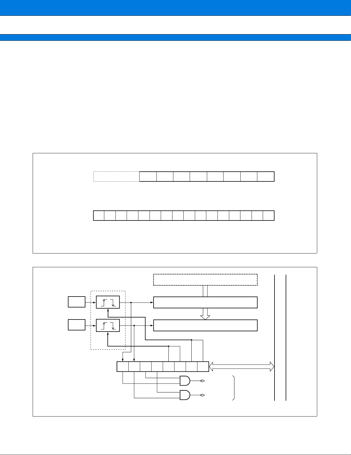
R : Read only
X : Indeterminate
•
Block diagram
P71/ASR1
P70/ASR0
Address
Edge detection circuit
Pin
Pin
Input capture
control status
register(ICS)
Input capture register 1 (IPCP1)
Input capture register 0 (IPCP0)
EG11 EG10 EG01 EG00
ICE0
16-bit free-run timer
Initial value
XXXXXXXX
XXXXXXXX
Internal data bus
B
B
40
*: Interrupt number
#17 (11H)
#15 (OF
Input capture
interrupt request
(ICU)
H
)
Page 41

MB90246A Series
7. Simple I/O Serial Interface
The 8/16-bit simple I/O serial interface transfers data synchronously with a clock.
• Communications direction: Concurrent processing of transmission (Whether data is to be sent or received
must be judged by the user.)
• Transfer mode: Clock synchronization function (Only data are transferred.)
• Transfer rate:DC to φ/2 (φ: Machine clock. Frequencies of up to 8 MHz are available when the machine clock
is rated at 16 MHz.)
• Shift clock: A machine clock division clock is used as the shift clock. (One of four division ratios can be
selected.). A shift clock is output only during data transfer.
• Data transfer format: MSB first can be selected. 8 or 16 bits can be selected as data length. Only data are
transferred.
• Interrupt request: An interrupt request is issued upon termination of transfer.
• Inter-CPU connection: Only 1:1 (bidirectional communication)
(1) Register Configuration
• Serial control status register 1, 2 (SCR)
Address
SCR0 : 000020
SCR1 : 000024
.............
bit 15 bit 8
H
H
(SSR)
bit 7 bit 6 bit 5 bit 4
OCKESTOP
R/W R/W R/W R/W R/W R/W R/W R/W
bit 3 bit 2 bit 1 bit 0
SIESOE WBSSIR SMD0SMD1
Initial value
10000000
B
• Serial status register 1, 2 (SSR)
Address
SSR1 : 000021
SSR2 : 000025
bit 15 bit 14 bit 13 bit 12 bit 11 bit 10 bit 9 bit 8
H
———————BUSY
H
———————R
• Serial data register 1, 2 (SDR)
Address
SDR1H : 000023
SDR2H : 000027
SDR1L : 000022
SDR2L : 000026
R/W:Readable and writable
R : Read only
— : Unused
X : Indeterminate
bit 15
bit 14bit 13bit 12bit 11bit 10 bit 9 bit 8 bit 7 bit 6 bit 5 bit 4 bit 3 bit 2 bit 1 bit 0
H
D15 D14 D13 D12 D11 D10 D09 D08 D07 D06 D05 D04 D03 D02 D01 D00
H
H
R/W R/W R/W R/W R/W R/W R/W R/W R/W R/W R/W R/W R/W R/W R/W R/W
H
.............
bit 7 bit 0
(SCR)
Initial value
-------1
Initial value
XXXXXXXX
XXXXXXXX
B
B
B
41
Page 42

MB90246A Series
(2) Block Diagram
Internal data bus
Serial data register (SDR)
Shift clock counter
STOP
Serial control
status register (SCR)
——————
Serial status register (SSR)
SDRH SDRL
Control circuit
2
OCKE
SOE
SIE WBS
SIR
—
SMD1 SMD0
BUSY
Pin
PA0/SID1
PA3/SID2
Pin
PA1/SOD1
PA4/SOD2
Pin
PA2/SCK1
PA5/SCK2
Serial I/O
interrupt request
H
#35 (23
#18 (12
)*
H
)*
: Machine clock frequency
φ
: Interrupt number
*
42
Page 43

MB90246A Series
8. UART
UART0 is a general-purpose serial data communication interface for performing synchronous or asynchronous
communication (start-stop synchronization system). In addition to the normal duplex communication function
(normal mode), UART0 has a master-slave type communication function (multi-processor mode).
• Data buffer: Full-duplex double buffer
• Transfer mode:Clock synchronized (with start and stop bit)
Clock asynchronized (start-stop synchronization system)
• Baud rate: With dedicated baud rate generator, selectable from 12 types
External clock input possible
Internal clock (A clock supplied from 16-bit re-load timer 2 can be used.)
• Data length: 7 bit to 9 bit selective (with a parity bit)
6 bit to 8 bit selective (without a parity bit)
• Signal format: NRZ (Non Return to Zero) system
• Reception error detection: Framing error
Overrun error
Parity error (not available in multi-processor mode)
• Interrupt request: Receive interrupt (receive complete, receive error detection)
Receive interrupt (transmit complete)
Transmit/receive conforms to extended intelligent I/O service (EI
• Master/slave type communication function: 1 (master) to n (slave) communication possible
(multi-processor mode)
(1) Register Configuration
2
OS)
• Status register (USR)
bit 15 bit 14 bit 13 bit 12 bit 11 bit 10 bit 9 bit 8Address
RDRF OREF PE TDRE RIE B CH0 RBF TBF (UMC)
H
000029
RRRRR/WR/WRR
• Mode control register (UMC)
Address
000028
H
............
bit 15 bit 8
• Rate and data register (URD)
bit 15 bit 14 bit 13 bit 12 bit 11 bit 10 bit 9 bit 8Address
H
00002B
BCH RC3 RC2 RC1 RC0 BCH0 P D8
R/W R/W R/W R/W R/W R/W R/W R/W
• Input data register (UIDR)
.....
bit 15 bit 9
H
00002A
(URD)
• Output data register (UODR)
Address
H
00002A
R/W:Readable and writable
R : Read only
W : Write only
X : Indeterminate
.....
bit 7 bit 0
bit 7 bit 6 bit 5 bit 4 bit 3 bit 2 bit 1 bit 0
PEN SBL MC1 MC0 SMDE RFC SCKE SOE(USR)
R/W R/W R/W R/W R/W W R/W R/W
bit 7 bit 0
bit 7 bit 6 bit 5 bit 4 bit 3 bit 2 bit 1 bit 0Address
bit 8
D7 D6 D5 D4 D3 D1 D0
D8
bit 8
RRRRR RRRR
bit 7 bit 6 bit 5 bit 4 bit 3 bit 2 bit 1 bit 0bit 15 bit 9
D7 D6 D5 D4 D3 D1 D0(URD) D8 D2
WWWWW WWWW
D2
.............
.............
(UIDR/UODR)
Initial value
00010000
Initial value
00000100
Initial value
00000000
Initial value
XXXXXXXX
Initial value
XXXXXXXX
B
B
B
B
B
43
Page 44

MB90246A Series
(2) Block Diagram
Dedicated baud
rate generator
16-bit re-load
timer 2
Pin
P96/SCK0
Clock
selector
Receive
clock
Start bit
detection circuit
Control bus
Receive
control circuit
Transmit
clock
Transmit
control circuit
Transmit start
circuit
Receive
interrupt signal
H
#39 (27
Transmit
interrupt signal
#37 (25
)*
H
)*
Pin
P94/SID0
Receive condition
decision circuit
UMC
register
Receive bit
Receive parity
Shift register for
reception
PEN
SBL
MC1
MC0
SMDE
RFC
SCKE
SOE
counter
counter
Reception
UIDR UODR
Internal data bus
register
complete
USR
Transmit bit
counter
Transmit parity
counter
Shift register for
transmission
RDRF
ORFE
PE
TDRE
RIE
TIE
RBF
TBF
URD
register
Pin
P95/SOD0
Start transmission
2
OS reception
To EI
error generation
signal (to CPU)
BCH
RC3
RC2
RC1
RC0
BCH0
P
D8
44
* : Interrupt number
Page 45

MB90246A Series
9. DTP/External Interrupt Circuit
The DTP (Data Transfer Peripheral)/external interrupt circuit is located between peripheral equipment connected
externally and the F
peripheral equipment to the CPU, generates external interrupt request and starts the extended intelligent I/O
service (EI
2
OS).
(1) Register Configuration
• DTP/interrupt factor register (EIRR)
Address
000031
• DTP/interrupt enable register (ENIR)
Address
000030
2
MC-16F CPU and transmit interrupt requests or data transfer requests generated by
............
bit 15 bit 14 bit 13 bit 12 bit 11 bit 10 bit 9 bit 8
H
RESV RESV RESV RESV ER3 ER2 ER1 ER0
————R/WR/WR/WR/W
............
bit 15 bit 8
H
bit 7 bit 6 bit 5 bit 4 bit 3 bit 2 bit 1 bit 0
RESV RESV RESV RESV EN3 EN2 EN1 EN0(EIRR)
— — — — R/W R/W R/W R/W
bit 7 bit 0
(ENIR)
Initial value
- -- - 0000
Initial value
- -- - 0000
B
B
• Request level setting register (ELVR)
Address
H
000032
R/W: Readable and writable
— : Unused
RESV : Reserved bit
............
bit 15 bit 8
bit 7 bit 6 bit 5 bit 4 bit 3 bit 2 bit 1 bit 0
LB3 LA3 LB2 LA2 LB1 LA1 LB0 LA0(Vacancy)
R/W R/W R/W R/W R/W R/W R/W R/W
Initial value
00000000
B
45
Page 46
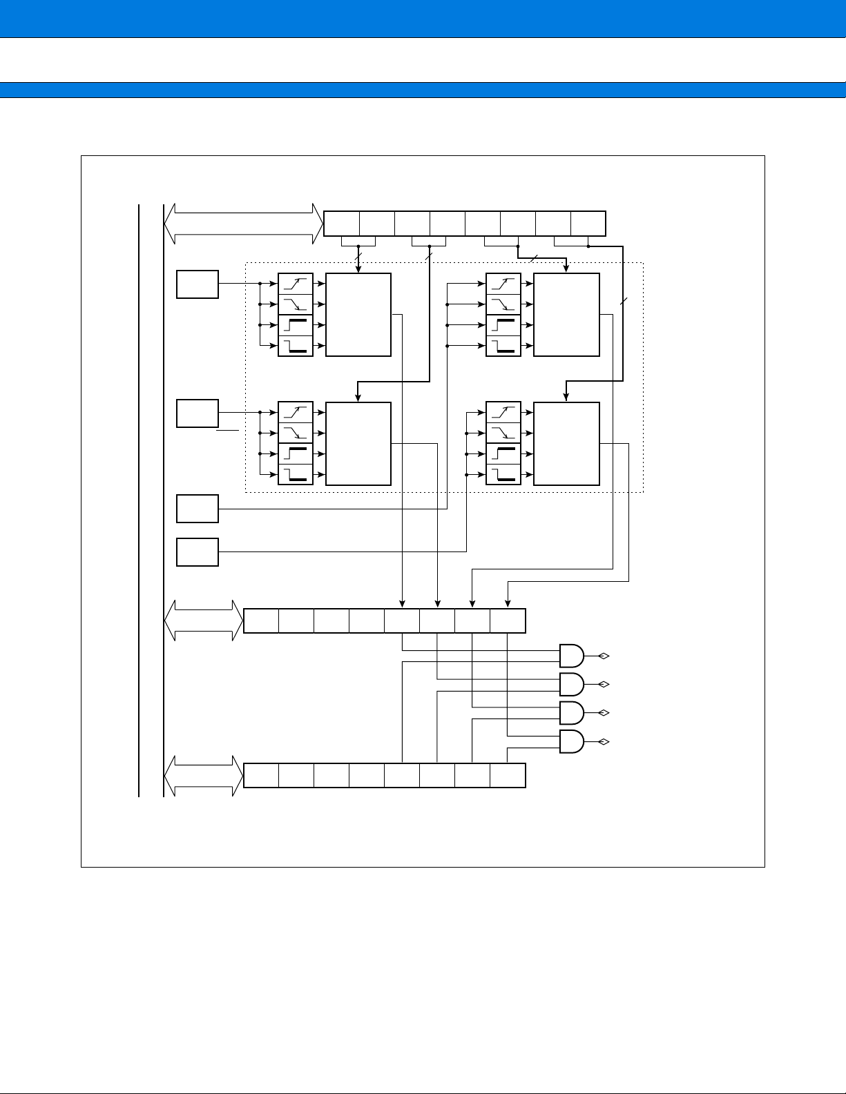
MB90246A Series
(2) Block Diagram
Request level setting register (ELVR)
LB3 LA3 LB2 LA2 LB1 LA1 LB0 LA0
Pin
P93/INT3/
PWM3
Pin
P92/INT2/ATG
s
u
b
a
t
a
d
l
Pin
a
n
r
e
P91/INT1
t
n
I
Pin
P90/INT0
22
Level edge
selector 3
Level edge
selector 2
DTP/external interrupt input
detection circuit
DTP/interrupt factor register
(EIRR)
RESV RESV RESV RESV ER3 ER2 ER1 ER0
2
2
Level edge
selector 1
Level edge
selector 0
Interrupt request signal
#21 (15H)*
46
*: Interrupt signal
DTP/interrupt enable register
(ENIR)
RESV RESV RESV RESV EN3 EN2 EN1 EN0
#19 (13
#13 (0D
#11 (0B
H
)*
H
)*
H
)*
Page 47

MB90246A Series
10. Delayed Interrupt Generation Module
The delayed interrupt generation module generates interrupts for switching tasks for development on a realtime operating system (REALOS series). The module can be used to generate softwarewise generates hardware
interrupt requests to the CPU and cancel the interrupts.
2
This module does not conform to the extended intelligent I/O service (EI
(1) Register Configuration
• Delayed interrupt factor generation/cancellation register (DIRR)
Address
00009F
bit 15 bit 14 bit 13 bit 12 bit 11 bit 10 bit 9 bit 8
H
———————R0
———————R/W
R/W: Readable and writable
— : Unused
OS).
............
bit 7 bit 0
(System reservation area)
Initial value
-------0
B
(2) Block Diagram
—
——————R0
Delayed interrupt factor generation/
cancellation register (DIRR)
*: Interrupt signal
Internal data bus
S factor
R latch
Interrupt request signal
H
#42 (2A
)*
47
Page 48

MB90246A Series
11. 8/10-bit A/D Converter
The 8/10-bit A/D converter has a function of converting analog voltage input to the analog input pins (input
voltage) to digital values (A/D conversion) and has the following features.
• Minimum conversion time: 6.13 µs (at machine clock of 16 MHz, including sampling time)
• Minimum sampling time: 3.75 µs (at machine clock of 16 MHz)
• Conversion time: The sampling time can be set arbitrarily.
Serial to parallel converter with a sample hold circuit
• Conversion method
• Resolution: 10-bit or 8-bit selective
• Analog input pins: Selectable from eight channels by software
Single conversion mode: Single conversion for the specified channel
Scan conversion mode: Scan conversions for maximum of four channel
• Interrupt requests can be generated and the extended intelligent I/O service (EI
end of A/D conversion.
• Starting factors for conversion: Selected from software activation, 16-bit re-load timer 1 output (rising edge),
and external trigger (falling edge).
• A data buffer that covers four channels is supported. The results of conversion are stored into the data buffer.
2
OS) can be started after the
48
Page 49

(1) Register Configuration
• A/D control status register upper digits (ADCSH)
Address
000071
bit 15 bit 14 bit 13 bit 12 bit 11 bit 10 bit 9 bit 8
H
— ACS2 ACS1 ACS0 — — CREG SCAN
— R/W R/W R/W — — R/W R/W
• A/D control status register lower digits (ADCSL)
Address
000070
bit 15 bit 8
H
bit 7 bit 6 bit 5 bit 4 bit 3 bit 2 bit 1 bit 0
BUSY INT INTE — STS1 STS0 STAR RESV(ADCSH)
............
R/W R/W R/W — R/W R/W R/W R/W
• A/D data register 0 to 3 (ADTH, ADTL)
Address
ADTH0 : 000075
ADTH1 : 000077
ADTH2 : 000079
ADTH3 : 00007B
ADTL0 : 000074
ADTL1 : 000076
ADTL2 : 000078
ADTL3 : 00007A
H
—
H
H
H
H
H
H
H
— — — — —D9D8D7D6D5D4D3D2D1D0
RRRRRR
bit 10bit 11bit 12bit 13bit 14bit 15
**
MB90246A Series
............
bit 7 bit 0
(ADCSL)
bit 7 bit 6 bit 5
RRRRRRRR
bit 4
bit 3bit 2bit 1bit 0bit 8bit 9
Initial value
- 000 - - 00
Initial value
000 - 0000
Initial value
------
XXXXXXXX
* *
B
B
B
B
• Conversion time setting register (ADCT)
Address
000073
000072
H
SMP3 SMP2 SMP1 SMP0 CV03 CV02 CV01 CV00 CV13 CV12 CV11 CV10 CV23 CV22 CV21 CV20
H
bit 10bit 11bit 12bit 13bit 14bit 15
• Analog input enable register (ADER)
Address
H
000016
R/W: Readable and writable
R : Read only
—:Unused
X : Indeterminate
* : The CREG bit value of ADCSH makes different storage styles.
RESV : Reserved bit
............
bit 15 bit 8
bit 7 bit 6 bit 5 bit 4 bit 3 bit 2 bit 1 bit 0
ADE7 ADE6 ADE5 ADE4 ADE3 ADE2 ADE1 ADE0(DDR7)
R/W R/W R/W R/W R/W R/W R/W R/W
bit 7 bit 6 bit 5
R/W R/W R/W
bit 4
R/W
bit 3bit 2bit 1bit 0bit 8bit 9
R/W R/W R/W R/WR/WR/WR/WR/WR/WR/WR/WR/W
Initial value
XXXXXXXX
XXXXXXXX
B
B
Initial value
11111111
B
49
Page 50

MB90246A Series
(2) Block Diagram
Conversion time setting register (ADCT)
SMP3
SMP2 SMP1 SMP0 CV03 CV02 CV01 CV00 CV13 CV12 CV11 CV10 CV23 CV22 CV21 CV20
4
4
4
4
Register selection
AVRH
AVRL
AV
CC
AV
SS
P67/AN7
P66/AN6
P65/AN5
P64/AN4
P63/AN3
P62/AN2
P61/AN1
P60/AN0
Analog
channel
selector
A/D data register 0 to 3
ADTH0 to ADTH3, ADTL0 to ADTL3
Sample
hold
A/D converter
circuit
Internal data bus
φ
TO
P92/INT2/ATG
Clock
selector
3
— ACS2 ACS1 ACS0 — — CREG SCAN BUSY INT INTE — STS1 STS0 STAR RESV
A/D control status register (ADCS)
φ : Machine clock frequency
TO : 16-bit re-load timer channel 1 output
Control circuit
2
Interrupt request #33 (21H)
50
Page 51

MB90246A Series
12. 8-bit D/A Converter
The 8-bit D/A converter, which is based on the R-2R system, supports 8-bit resolution mode. It contains two
channels each of which can be controlled in terms of output by the D/A control register.
(1) Register Configuration
• D/A control register 0 (DACR0)
.............
bit 15 bit 14 bit 13
H
00005B
———
———
• D/A control register 1 (DACR1)
bit 15 bit 14 bit 13
H
00005D
———
———
• D/A control register 2 (DACR2)
bit 12
—
—
bit 12
—
—
bit 11 bit 10 bit 9 bit 8Address
———DAE0
———R/W
bit 11 bit 10 bit 9 bit 8Address
———DAE1
———R/W
bit 7 bit 0
(DADR0)
.............
bit 7 bit 0
(DADR1)
Initial value
-------0
Initial value
-------0
B
B
Address
00005F
bit 15 bit 14 bit 13
H
———
———
• D/A data register 0 (DADR0)
............
Address
00005A
bit 15 bit 8
H
(DACR0) DA07 DA06 DA05
• D/A data register 1 (DADR1)
............
Address
00005C
bit 15 bit 8
H
(DACR1) DA17 DA16 DA15
• D/A data register 2 (DADR2)
............
Address
00005E
R/W:Readable and writable
—:Unused
X : Indeterminate
bit 15 bit 8
H
(DACR2) DA27 DA26 DA25
bit 11 bit 10 bit 9 bit 8
bit 12
———DAE2
—
———R/W
—
bit 7 bit 6 bit 5
R/W R/W R/W
bit 7 bit 6 bit 5
R/W R/W R/W
bit 7 bit 6 bit 5
R/W R/W R/W
bit 7 bit 0
bit 3 bit 2 bit 1 bit 0
bit 4
DA03 DA02 DA01 DA00
DA04
R/W R/W R/W R/W
R/W
bit 3 bit 2 bit 1 bit 0
bit 4
DA13 DA12 DA11 DA10
DA14
R/W R/W R/W R/W
R/W
bit 3 bit 2 bit 1 bit 0
bit 4
DA23 DA22 DA21 DA20
DA24
R/W R/W R/W R/W
R/W
.............
(DADR2)
Initial value
-------0
Initial value
XXXXXXXX
Initial value
XXXXXXXX
Initial value
XXXXXXXX
B
B
B
B
51
Page 52

MB90246A Series
(2) Block Diagram
D/A data register (DADR0)
<DADR1> <DADR2>
DA×7
Internal data bus
DA×6DA×5DA×4DA×3DA×2DA×1DA×0
D/A converter
DVRH
DA×7
2R
2R
2R
R
R
R
DA×6
DA×5
DA×4
Pin
P82/DAO0
<P83/DAO1>
<P84/DAO2>
2R
2R
2R
2R
2R
DVRL
R
R
R
R
R
DAE———————
DA×3
DA×2
DA×1
DA×0
Standby control
D/A control register (DACR0)
<DACR1> <DACR2>
Internal data bus
Note: The 8-bit D/A converter supports channels 0 to 2. A value enclosed by < and >
is for channels 1 and 2.
52
Page 53
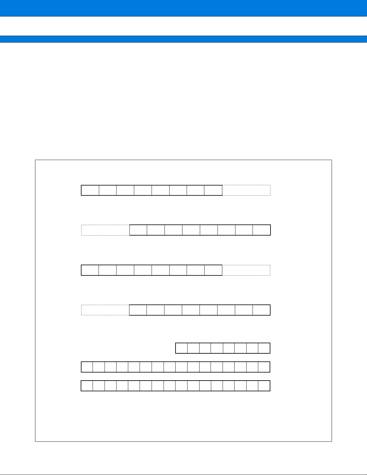
MB90246A Series
13. DSP Interface for the IIR Filter
The DSP interface for the IIR filter is a unit which covers product addition (ΣBi × Yj + ΣAm × Xn) by hardware.
This interface allows IIR filter calculation to be performed readily and in a high speed.
The DSP interface for the IIR filter has the following features.
• Coefficients A and B, and variables X and Y have 16-bit length, and four banks are supported.
• (1 to 4) + (1 to 4) product terms can be selected.
• Data can be rounded and clipped in units of 10 or 12 bits.
• With two or more concatenated banks used, the results of an operation can be transferred to the subsequent
bank register.
• Operation time: ((M + N + 1) × B + 1)/φ µs(M, N = number of product terms, B = number of banks, φ: machine
clock)
(1) Register Configuration
• Product addition control status register upper digits (MCSR:H)
.............
bit 7 bit 0
(MCSR:L)
Initial value
-XXXXXXX
B
000081
bit 15 bit 14 bit 13
H
—WEYWENY
—R/WR/W
bit 12
WENX
R/W
bit 11 bit 10 bit 9 bit 8Address
N1 N0 M1 M0
R/W R/W R/W R/W
• Product addition control status register lower digits (MCSR:L)
Address
000080
bit 15 bit 8
H
(MCSR:H) RND CLP DIV
bit 7 bit 6 bit 5
R/W R/W R/W
bit 4
BF
R
............
• Product addition control register upper digits (MCCR:H)
000083
bit 15 bit 14 bit 13
H
———
———
bit 12
—
—
bit 11 bit 10 bit 9 bit 8Address
— — RESV RESV
——R/WR/W
• Product addition control register lower digits (MCCR:L)
Address
000082
bit 15 bit 8
H
(MCCR:H) OVF CNTD CNTC
bit 7 bit 6 bit 5
R/W R/W R/W
bit 4
CNTB
R/W
............
• Product addition output register (MDORL, M, H)
Address
MDORH : 000088
MDORM : 000086
MDORL : 000084
H
H
H
bit 10bit 11bit 12bit 13bit 14bit 15
bit 7 bit 6 bit 5
SSSSSD34D33D32
RRRRRRRR
D23 D22 D21
RRRRRRRRRRRRRRRR
D7 D6 D5
RRRRRRRRRRRRRRRR
bit 3 bit 2 bit 1 bit 0
BNK1 BNK0 TRG MAE
R/W R/W W R/W
.............
bit 7 bit 0
(MCCR:L)
bit 3 bit 2 bit 1 bit 0
CDRD CDRC CDRB CDRA
R/W R/W R/W R/W
bit 3bit 2bit 1bit 0bit 8bit 9
bit 4
D19 D18 D17 D16D24D25D26D27D28D29D30D31
D20
D3 D2 D1 D0D8D9D10D11D12D13D14D15
D4
Initial value
XXX0XXX0
Initial value
------00
Initial value
00000000
Initial value
XXXXXXXX
XXXXXXXX XXXXXXXX
XXXXXXXX XXXXXXXX
B
B
B
B
B
B
R/W: Readable and writable
R : Read only
W : Write only
— : Unused
X : Indeterminate
RESV : Reserved bit
53
Page 54

MB90246A Series
(2) Block Diagram
Internal data bus
Transfer data
Transfer data
selector
Coefficient registerCoefficient register
A0 to A3 B0 to B3 X0 to X3 Y0 to Y3
Coefficient register
selector
Input data selector
Product addition unit
Input data register Input data register
Register selection
Register
selection
Bank/register
Product adder
4
Right shift and clip
OVF CNTD CNTC
CDRD CDRC CDRB CDRA
CNTB
Product addition control register (MCCR)
Product addition output register L
(MDORL)
Product addition output register M
(MDORM)
Product addition
output register H
(MDORH)
selector
selector
3
Bank
selection
Register
selection
54
4
3
— WEY WENY
N1 N0 M1 M0 RND CLP DIV BF BNK1 BNK0 TRG MAE
WENX
Product addition control status register (MCSR)
2
Page 55

MB90246A Series
14. Low-power Consumption (Stand-by) Mode
The F2MC-16F has the following CPU operating mode configured by selection of an clock operation control.
• Stand-by mode
The hardware stand-by mode is a mode for reducing power consumption by stopping clock supply to the CPU
by the low-power consumption control circuit, and stopping oscillation clock (stop mode, hardware standby
mode).
Gear function contributes to the low-power dissipation by providing options of divide-by-2, 4, or 16 external
clock frequencies, whichiare usually derived from non-divided frequencies.
(1) Register Configuration
• Standby control register (STBYC)
Address
H
0000A0
R/W:Readable and writable
W : Write only
X : Indeterminate
............
bit 15 bit 8
bit 7 bit 6 bit 5 bit 4 bit 3 bit 2 bit 1 bit 0
STP SLP SPL RST OSC1 OSC0 CLK1 CLK0(Vacancy)
W W R/W R/W R/W R/W R/W R/W
Initial value
0001XXXX
B
55
Page 56

MB90246A Series
(2) Block Diagram
Low-power consumption mode control register (STBYC)
STP SLP SPL RST OSC1 OSC0 CLK1 CLK0
Pin
high-impedance
control circuit
Pin Hi-z control
RST
Pin
Cancellation of reset
Cancellation of interrupt
HST
Pin
Clock
generation
block
X0 Pin
X0 Pin
Clock selector
Divided
-by-2
System clock
generation
circuit
Oscillation
clock
2
2
Divided
-by-2
DDC
Standby control
circuit
Machine clock
Cancellation of
oscillation
stabilization time
Divided
-by-4
Main clock
Divided
-by-2
Internal reset
generation
circuit
CPU clock
control circuit
RST
Peripheral clock
control circuit
2
14
Divided
-by-2
Divided
-by-2
Internal reset
CPU clock
Stop and sleep signal
Stop signal
Peripheral clock
Oscillation
stabilization
time selector
Divided
-by-2
Timebase timer
56
DDC: Direct duty control
Page 57

ELECTRICAL CHARACTERISTICS
■
1. Absolute Maximum Ratings
Parameter
MB90246A Series
Symbol
Min. Max.
V
CC VSS – 0.3 VSS + 7.0 V
AV
CC VSS – 0.3 VSS + 7.0 V *1
Value
Unit Remarks
(AVSS = VSS = 0.0 V)
Power supply voltage
Input voltage V
Output voltage V
“L” level maximum output current I
AVRH,
AVRL
DVRH,
DVRL
I VSS – 0.3 VCC + 0.3 V *2
O VSS – 0.3 V CC + 0.3 V *2
OL 10 mA *3
SS – 0.3 VSS + 7.0 V *1
V
V
SS – 0.3 VSS + 7.0 V *1
“L” level average output current IOLAV 4mA*4
“L” level total average output current ΣI
“H” level maximum output current I
OLAV 50 mA *5
OH –10 mA *3
“H” level average output current IOHAV –4 mA *4
“H” level total average output current ΣI
Power consumption P
Operating temperature T
OHAV –48 mA *5
D 600 mW
A –30 +70 °C
Storage temperature Tstg –55 +150 °C
*1: AV
CC, AVRH, AVRL, DVRH and DVRL shall never exceed VCC.
DVRL shall never exceed DVRH. AVRL shall never exceed AVRH.
*2: V
I and VO shall never exceed VCC + 0.3 V.
*3: The maximum output current is a peak value for a corresponding pin.
*4: Average output current is an average current value observed for a 100 ms period for a corresponding pin.
*5: Total average current is an average current value observed for a 100 ms period for all corresponding pins.
WARNING: Semiconductor devices can be permanently damaged by application of stress (voltage, current,
temperature, etc.) in excess of absolute maximum ratings. Do not exceed these ratings.
57
Page 58

MB90246A Series
2. Recommended Operating Conditions
Parameter
Power supply voltage
Symbol
V
CC 4.5 5.5 V Normal operation
CC 2.0 5.5 V
V
Min. Max.
(AVSS = VSS = 0.0 V)
Value
Unit Remarks
Retains RAM data at the time of
operation stop
Operating temperature T
WARNING: The recommended operating conditions are required in order to ensure the normal operation of the
semiconductor device. All of the device's electrical characteristics are warranted when the device is
operated within these ranges.
Always use semiconductor devices within their recommended operating condition ranges. Operation
outside these ranges may adversely affect reliability and could result in device failure.
No warranty is made with respect to uses, operating conditions, or combinations not represented on
the data sheet. Users considering application outside the listed conditions are advised to contact their
FUJITSU representatives beforehand.
A –30 +70 °C External bus mode
58
Page 59

3. DC Characteristics
(AVCC = VCC = 4.5 V to 5.5 V, AVSS = VSS = 0.0 V, TA = –30°C to +70°C)
Parameter Symbol Pin name Condition
V
IH CMOS input pin — 0.7 VCC —VCC + 0.3 V
“H” level
input
voltage
“L” level
input
voltage
“H” level
output
voltage
“L” level
output
voltage
Open-drain
output
leakage
current
“H” level
input
current
“L” level
input
current
Pull-up
resistance
VIH2 TTL input pin VCC = 5.0 V ±10% 2.2 — VCC + 0.3 V
IH1S
V
IHM MD0 to MD2 VCC – 0.3 — VCC + 0.3 V
V
Hysteresis input
pin
—
VIL1 CMOS input pin VCC – 0.3 — 0.3 VCC V
VIL2 TTL input pin VCC = 5.0 V ±10% VCC – 0.3 — 0.8 V
IL1S
V
ILM MD0 to MD2 VCC – 0.3 — VCC + 0.3 V
V
V
OH
V
OL All output pins
I
LEAK P60 to P67 — — 0.1 10 µA
IH1
I
IH2 TTL input pin
I
I
IH3
IL1
I
IL2 TTL input pin
I
IL3
I
RRST
Hysteresis input
pin
All ports other
than P60 to P67
CMOS input
pins other than
RST
Hysteresis input
pin
CMOS input
pins other than
RST
Hysteresis input
pin
—
VCC = 4.5 V
I
OH = –4.0 mA
CC = 4.5 V
V
I
OL = 4.0 mA
VCC = 5.5 V
V
IH = 0.7 VCC
CC = 5.5 V
V
VIH = 2.2 VCC
VCC = 5.5 V
VIH = 0.8 VCC
VCC = 5.5 V
V
IL = 0.3 VCC
V
CC = 5.5 V
V
IL = 0.8 V
VCC = 5.5 V
V
IL = 0.2 VCC
— 22 — 110 kΩ
MB90246A Series
Value
Min. Typ. Max.
CC —VCC + 0.3 V
0.8 V
CC – 0.3 — 0.2 VCC V
V
CC – 0.5 — — V
V
——0.4V
— — –10 µA
— — –10 µA
— — –10 µA
——10µA
——10µA
——10µA
Unit Remarks
(Continued)
59
Page 60

MB90246A Series
(Continued)
(AVCC = VCC = 4.5 V to 5.5 V, AVSS = VSS = 0.0 V, TA = –30°C to +70°C)
Parameter Symbol Pin name Condition
Internal operation
at 16 MHz
V
CC = 5.0 V ±10%
Normal operation
Internal operation
at 16 MHz
V
CC = 5.0 V ±10%
In sleep mode
A = +25°C
T
V
CC = 4.5 V to 5.5 V
In stop mode and
hardware standby
mode
——10—pF
Power
supply
current
Input
capacitance
I
CC VCC
CCS —
I
I
CCH —
C
IN
Other than AVCC,
AV
SS, VCC, VSS
Value
Unit Remarks
Min. Typ. Max.
— 80 100 mA
—3050mA
—0.110µA
60
Page 61

4. AC Characteristics
(1) Reset, Hardware Standby Input Timing
Parameter
Reset input time t
Hardware standby input time t
Symbol Pin name Condition
RSTL RST
HSTL HST 5 tCYC*— ns
MB90246A Series
(AV
CC = VCC = 4.5 V to 5.5 V, AVSS = VSS = 0.0 V, TA = –30°C to +70°C)
—
Value
Min. Max.
5 t
CYC*— ns
Unit Remarks
* :For t
CYC (cycle time (machine cycle)), see paragraph (4), "Clock output timing."
Note: Upon hardware standby input, divide-by-32 is selected as the machine cycle.
tRSTL, tHSTL
RST
HST
0.2 V
CC
0.2 V
• Measurement conditions for AC ratings
Pin
L
C
CL is a load capacitance connected to a pin under test.
L
Capacitors of C
to address bus (A23 to A00) and data bus (D15 to D00), RD
= 30 pF should be connected to CLK pin, while CL of 80 pF is connected
, WRH and WRL pins.
CC
61
Page 62

MB90246A Series
(2) Specification for Power-on Reset
Parameter
Power supply rising time t
Power supply cut-off time t
* :V
CC must be kept lower than 0.2 V before power-on.
Notes: • The above ratings are values for causing a power-on reset.
• When HST
is set to “L”, apply power according to this table to cause a power-on reset irrespective of
whether or not a power-on reset is required.
• For built-in resources in the device, re-apply power to the resources to cause a power-on reset.
Symbol Pin name Condition
R VCC
OFF VCC 1—ms
tR
—
(AV
SS = VSS = 0.0 V, TA = –30°C to +70°C)
Value
Min. Max.
Unit Remarks
—30ms*
Due to repeated
operations
0.2 V
4.5 V
0.2 V 0.2 V
tOFF
It is recommended to keep the rising
speed of the supply voltage at 50 mV/ms.
RAM data retained
CC
V
Sudden changes in the power supply voltage may cause a power-on reset.
To change the power supply voltage while the device is in operation, it is recommended to raise the voltage
smoothly to suppress fluctuations as shown below.
Main power
supply voltage
CC
V
Sub power supply voltage
SS
V
62
Page 63

(3) Clock Timings
• Operation at 5.0 V ±10%
Parameter
Clock frequency F
Symbol Pin name Condition
C X0, X1 VCC = 5.0 V ±10% 16 — 32 MHz
Clock cycle time tC X0, X1
Input clock pulse
width
Input clock rising/
falling time
P
P
t
t
WH,
WL
CR,
CF
X0 10 — — ns
X0 VCC = 5.0 V ±10% — — 11 ns
•Clock timings
—
MB90246A Series
(AV
SS = VSS = 0.0 V, TA = –30°C to +70°C)
Value
Min. Typ. Max.
1/Fc — — ns
tC
Unit Remarks
Recommended
duty ratio of
30% to 70%
Maximum value
CR + tCF
= t
0.7 V
CC
WH
P
0.7 V
0.3 V
CC
CC
PWL
CF
t
• Relationship between clock frequency and power supply voltage
(V)
CC
5.5
4.5
Power supply voltage V
0
Clock frequency F
Normal operation range
A
= –30°C to +70°C)
(T
16 (MHz)
C
32
0.7 V
0.3 V
CC
CC
CR
t
63
Page 64

MB90246A Series
(4) Clock Output Timing
Parameter
Cycle time
(machine cycle)
CLK ↑ → CLK ↓ t
Symbol Pin name Condition
t
CYC CLK —
CHCL CLK VCC = 5.0 V ±10% 1 tCYC/2 – 20 1 tCYC/2 + 20 ns
(AV
CC = VCC = 4.5 V to 5.5 V, AVSS = VSS = 0.0 V, TA = –30°C to +70°C)
Value
Min. Max.
1
2 t
C*
32tC*1*
Unit Remarks
2
ns
*1: For t
C (clock cycle time), refer to “(3) Clock Timings.”
*2: This case is applied when the lowest speed (1/16) is selected by the clock gear function with the clock frequency
(F
C) set at 16 MHz.
CYC
t
CHCL
t
CLK
2.4 V
0.8 V
2.4 V
64
Page 65

MB90246A Series
(3) Bus Read Timing
(AV
CC = VCC = 2.7 V to 5.5 V, AVSS = VSS = 0.0 V, TA = –40°C to +85°C)
Parameter
Effective address →
RD
↓ time
Effective address →
effective data input
RD
pulse width tRLRH RD —
RD
↓ → effective data
input
↑ → data hold time tRHDX D15 to D00
RD
↑ → address
RD
effective time
Effective address →
CLK ↑ time
RD
↓ → CLK ↑ time tRLCL RD, CLK 1 tCYC*/2 – 25 — ns
Symbol Pin name Condition
t
AVRL A00 to A23
V
CC = 5.0 V ±10%
AVDV D15 to D00 —
t
CYC*/2 – 20 — ns
1 t
(N + 1) ×
CYC* – 25
1 t
RLDV D15 to D00 VCC = 5.0 V ±10% —
t
RHAX A00 to A23 1 tCYC*/2 – 20 — ns
t
—
1 t
CYC*/2 – 25 — ns
t
AVCH
CLK,
A00 to A23
Value
Min. Max.
(N + 1.5) ×
1 t
CYC* – 40
—ns
(N + 1) ×
1 t
CYC** – 30
0—ns
Unit
ns
ns
Remarks
N: Stands for the number of wait cycles. With no wait, N is set at “0”. (The number of wait cycles depends on an
automatic wait and external RDY.)
* :For t
CYC (cycle time (machine cycle)), see paragraph (4), “Clock output timing.”
CLK
RD
A00 to A23
D00 to D15
t
0.8 V
2.4 V
0.8 V
AVCH
AVRL
t
AVDV
t
2.4 V
0.8 V
RLCL
t
RLDV
t
RLRH
t
0.8 V
2.2 V
0.8 V
2.4 V
tRHAX
2.4 V
0.8 V
RHDX
t
2.2 V
0.8 V
65
Page 66

MB90246A Series
(4) Bus Write Timing
(AV
CC = VCC = 4.5 V to 5.5 V, AVSS = VSS = 0.0 V, TA = –30°C to +70°C)
Parameter
Effective address →
WRL
, WRH ↓ time
, WRH pulse width tWLWH WRL, WRH
WRL
Write data → WRL
WRH
↑ time
WRL
, WRH ↑ → data
,
hold time
, WRH ↑ →
WRL
address effective time
WRL
, WRH ↓ → CLK ↓
time
Symbol Pin name Condition
t
AVWL A00 to A23 VCC = 5.0 V ±10%
t
DVWH D15 to D00
WHDX D15 to D00 VCC = 5.0 V ±10%
t
t
WHAX A00 to A23
t
WLCL WRL, CLK
—
1 t
(N + 1) ×
1 t
CYC** – 25
(N + 1) ×
1 t
1 t
1 t
1 t
Value
Min. Max.
CYC*/
2 – 20
—ns
—ns
CYC* – 40
CYC*/
2 – 20
CYC*/
2 – 20
CYC*/
2 – 25
—ns
—ns
—ns
—ns
N: Stands for the number of wait cycles. With no wait, N is set at “0”. (The number of wait cycles depends on an
automatic wait and external RDY.)
Unit
Remarks
* :For t
CLK
WRL, WRH
A00 to A23
D00 to D15
CYC (cycle time (machine cycle)), see paragraph (4), “Clock output timing.”
WLCL
t
0.8 V
AVWL
t
2.4 V
0.8 V
0.8 V
WLWH
t
tDVWH tWHDX
2.4 V
0.2 V
Write data
2.4 V
t
WHAX
2.4 V
0.8 V
2.4 V
0.2 V
66
Page 67

MB90246A Series
(5) Ready Input Timing
• CLK signal standards
(AV
CC = VCC = 4.5 V to 5.5 V, AVSS = VSS = 0.0 V, TA = –30°C to +70°C)
Parameter
RD
/WRH/WRL ↓ →
RDY ↓ time
RDY setup time
(in diallocating)
RDY hold time t
Symbol Pin name Condition
RD/WRH/
RYHS
t
WRL
,
RDY
RHDV RDY VCC = 5.0 V ±10% 30 — ns
t
RYHH RDY — 0 — ns
N: Stands for the number of wait cycles. With no wait, N is set at “0”. (The number of wait cycles depends on an
automatic wait and external RDY.)
Value
Min. Max.
0
N ×1 t
+ 15
Unit Remarks
CYC*
ns
* :For t
CYC (cycle time (machine cycle)), see paragraph (4), “Clock output timing.”
Note: Use the automatic ready function when the setup time for the rising edge of the RDY signal is not sufficient.
• Ready input timing (CLK signal standards)
CLK
A00 to A23
RD/WRH/WRL
RDY
(wait not inserted)
RDY
(wait inserted)
0.8 V
RYH
t
2.2 V 2.2 V
0.8 V 0.8 V
RYHH
t
2.2 V 2.2 V
RHDV
t
RYHH
t
67
Page 68

MB90246A Series
•RD/WRH/WRL signal standards
(AV
CC = VCC = 4.5 V to 5.5 V, AVSS = VSS = 0.0 V, TA = –30°C to +70°C)
Parameter
RD
/WRH/WRL ↓ →
RDY ↓ time
RDY pulse width t
Symbol Pin name Condition
RD/WRH/
t
RYHS
WRL,
—0
RDY
RYPW RDY VCC = 5.0 V ±10%
1/2 t
RD/WRH/
RDY ↑ → RD
↑ tRHDV
WRL
,
—
RDY
N: Stands for the number of wait cycles. With no wait, N is set at “0”. (The number of wait cycles depends on an
automatic wait and external RDY.)
m: Stands for the number of RDY wait cycles. With no wait, m is set at “0”.
*1: Use the automatic ready function when the setup time is not sufficient.
*2: If the pulse width has exceeded the maximum value, the wait period may be extended beyond the specified
number of cycles by one cycle.
*3: For t
CYC (cycle time (machine cycle)), see paragraph (4), “Clock output timing.”
Value
Min. Max.
N ×1 t
+ 15*
3
(m + 1) × 1
3
tCYC*2,*
2 t
– 25
+ 20
1 t
– 15
CYC*
CYC*
CYC*
CYC*
Unit Remarks
3
ns
1
ns
3
3
ns
• Ready input timing (RD/WRH/WRL signal standards)
A00 to A23
RD/WRH/WRL
RDY
(wait not inserted)
RDY
(wait inserted)
0.8 V
2.2 V
0.8 V
t
RYHS
RYPW
t
2.2 V
0.8 V
2.2 V
RHDV
t
2.4 V
68
Page 69

MB90246A Series
(8) Hold Timing
(AV
CC = VCC = 4.5 V to 5.5 V, AVSS = VSS = 0.0 V, TA = –30°C to +70°C)
Parameter
Pins in floating status →
↓ time
HAK
HAK
↑ → pin valid time tHAHV HAK —1 tCYC*2 tCYC*ns
Symbol Pin name Condition
t
XHAL HAK VCC = 5.0 V ±10% 30 1 tCYC*ns
Value
Min. Max.
Unit Remarks
* :For t
Note: More than 1 machine cycle is needed before HAK
CYC (cycle time (machine cycle)), see paragraph (4), “Clock output timing.”
changes after HRQ pin is fetched.
HRQ
HAK
Pins
t
0.8 V
XHAL
High impedance
2.4 V
HAHV
t
(9) UART Timing
(AV
CC = VCC = 4.5 V to 5.5 V, AVSS = VSS = 0.0 V, TA = –30°C to +70°C)
Parameter
Serial clock cycle time t
SCK ↓ → SOD delay
time
Valid SID → SCK ↑ tIVSH
SCK ↑ → valid SID hold
time
Serial clock “H” pulse
width
Serial clock “L” pulse
width
SCK ↓ → SOD delay
time
Valid SID → SCK ↑ tIVSH —60—ns
SCK ↑ → valid SID hold
time
Symbol Pin name Condition
SCYC SCK0 — 8 tCYC*—ns
t
SLOV
t
SHIX
t
SHSL SCK0
SCK0,
SOD0
SCK0,
SID0
SCK0,
SID0
V
CC = 5.0 V ±10%
—
t
SLSH SCK0 4 tCYC*—ns
t
SLOV
t
SHIX
SCK0,
SID0
SCK0,
SID0
V
CC = 5.0 V ±10%
Value
Min. Max.
–80 80 ns
Unit Remarks
Internal shift
clock mode
C
100 — ns
L = 80 pF for
an output pin
60 — ns
4 tCYC*—ns
External shift
clock mode
C
— 150 ns
L = 80 pF for
an output pin
60 — ns
* :For t
CYC (cycle time (machine cycle)), see paragraph (4), “Clock output timing.”
Notes: • These are AC ratings in the CLK synchronous mode.
•C
L is the load capacitor value connected to pins while testing.
69
Page 70

MB90246A Series
• Internal shift clock mode
SCK0
SOD0
SID0
• External shift clock mode
SCK0
SOD0
0.8 V
tSLOV
0.2 V
tSLOV
tSCYC
2.4 V
2.4 V
0.8 V
tIVSH tSHIX
CC
0.8 V
CC
0.2 V
tSLSH tSHSL
0.8 V
CC
0.2 V
CC
2.4 V
0.8 V
0.8 V
CC
0.8 V
CC
0.2 V
CC
0.8 V
CC
70
SID0
tIVSH tSHIX
CC
0.8 V
CC
0.2 V
0.8 V
0.2 V
CC
CC
Page 71

(10) Timer Input Timing
Parameter
Input pulse width
(AV
CC = VCC = 4.5 V to 5.5 V, AVSS = VSS = 0.0 V, TA = –30°C to +70°C)
Symbol Pin name Condition
TIWH,
t
tTIWL
ASR0, ASR1,
TIN0 to TIN2
—4 t
MB90246A Series
Value
Min. Max.
CYC*—ns
Unit Remarks
* :For t
CYC (cycle time (machine cycle)), see paragraph (4), “Clock output timing.”
ASR0, ASR1
TIN0 to TIN2
(11) Timer Output Timing
Parameter
CLK ↑ → TOT
transition time
0.8 V
CC
tTIWH
(AV
CC = VCC = 4.5 V to 5.5 V, AVSS = VSS = 0.0 V, TA = –30°C to +70°C)
0.8 V
0.2 V
CC
Symbol Pin name Condition
TOT0 to TOT2,
t
TO
PWM0 to
V
CC = 5.0 V ±10% — 40 ns
PWM3
2.4 V
CLK
CC
tTIWL
Value
Min. Max.
CC
0.2 V
Unit Remarks
TOT
2.4 V
0.8 V
TO
t
71
Page 72

MB90246A Series
(12) I/O Simple Serial Timing
Parameter
Serial clock cycle time t
SCK ↓ → SOD delay
time
Valid SID → SCK ↑ t
SCK ↑ → valid SID hold
time
Symbol Pin name Condition
SCYC SCK1, SCK2
SLOV
t
IVSH
SHIX
t
SCK1, SOD1,
SCK2, SOD2,
SCK1, SID1,
SCK2, SID2,
SCK1, SID1,
SCK2, SID2,
(AV
CC = VCC = 4.5 V to 5.5 V, AVSS = VSS = 0.0 V, TA = –30°C to +70°C)
Value
Min. Max.
Unit Remarks
2 tCYC*—ns
CYC*/2 ns
Internal shift
clock mode
C
L = 80 pF for
—
—1 t
CYC*—ns
1 t
an output pin
CYC*—ns
1 t
* :For t
Note: C
CYC (cycle time (machine cycle)), see paragraph (4), “Clock output timing.”
L is the load capacitor value connected to pins while testing.
• Internal shift clock mode
SCK1, SCK2
SOD1, SOD2
SID1, SID2
0.8 V
tSLOV
tSCYC
2.4 V
2.4 V
0.8 V
tIVSH tSHIX
CC
0.8 V
CC
0.2 V
0.8 V
0.8 V
0.2 V
CC
CC
72
Page 73

(13) Trigger input timing
Parameter
Input pulse width
(AV
CC = VCC = 4.5 V to 5.5 V, AVSS = VSS = 0.0 V, TA = –30°C to +70°C)
Symbol Pin name Condition
TRGH,
t
t
TRGL
ATG,
INT0 to INT3
—5 t
MB90246A Series
Value
Min. Max.
CYC*—ns
Unit Remarks
* :For t
CYC (cycle time (machine cycle)), see paragraph (4), “Clock output timing.”
CC
0.8 V
0.2 V
CC
tTRGL
ATG
INT0 to INT3
0.8 V
CC
tTRGH
0.2 V
CC
73
Page 74

MB90246A Series
5. A/D Converter Electrical Characteristics
(AVCC = VCC = 4.5 V to 5.5 V, AVSS = VSS = 0.0 V, TA = –30°C to +70°C)
Parameter
Resolution — —
Symbol Pin name Condition
Min. Typ. Max.
— 8, 10 10 bit
Total error — — — — ±3.0 LSB
Linearity error — — — — ±2.0 LSB
Differential linearity error — — — — ±1.9 LSB
Zero transition voltage V
Full-scale transition
voltage
Conversion time*
1
Sampling
period
Conversion
period a
Conversion
period b
Conversion
period c
Analog port input current I
Analog input voltage V
OT AN0 to AN7
FST AN0 to AN7
V
——
— — 560 — — ns
— — 125 — — ns
Use the A/D data
register for setup.
V
CC = 5.0 V ±10%
— — 125 — — ns
— — 250 — — ns
AIN AN0 to AN7
AIN AN0 to AN7 AVRL — AVRH V
— AVRH
Reference voltage
AVRH – AVRL 2.7
—
—
AVRL
– 1.0 LSB
AVRH
– 4.0 LSB
1.25 — — µs
—0.13µA
AVRL
≥
+ 2.7
— AVRL 0 —
A AVCC — — 15 20 mA
I
Power supply current
Reference voltage
supply current
2
I
AS*
R AVRH — — 0.7 2 µA
I
2
I
RS*
AVCC
AVRH
Supply current when
the CPU stops
(AV
CC = 5.5 V)
Supply current when
the CPU stops
(AV
CC = 5.5 V)
—— 5µA
—— 5µA
Offset between channels — AN0 to AN7 — — — 4 LSB
Value
AVRL
+ 1.0 LSB
AVRH
– 1.0 LSB
AVRL
+ 3.0 LSB
AVRH
+ 1.0 LSB
—AV
AVRH
– 2.7
Unit
CC V
mV
mV
V
*1: Glossary for conversion time
Conversion time
CYC
Sampling period
*
ADCS bit 1: Sets STAR
Conversion period a Conversion period b Conversion period c
End of conversionA/D activation
CYC
2 t
*1 t
ADCS bit 6: INT “H”
(Interrupt occurred to CPU)
* :For tCYC, see ■ Electrical Characteristics, 4, “AC Characteristics,” Cycle time (machine cycle) in
paragraph (4), “Clock output timing.”
*2: IAS and IRS signify currents when the A/D converter does not operate and when the CPU is out of service,
respectively.
74
Page 75

MB90246A Series
6. A/D Converter Glossary
Resolution: Analog changes that are identifiable with the A/D converter
With 10 bits supported, an analog voltage can be divided into 2
Linearity error: The deviation of the straight line connecting the zero transition point (“00 0000 0000” ↔ “00
0000 0001”) with the full-scale transition point (“11 1111 1110” ↔
conversion characteristics
Differential linearity error: The deviation of input voltage needed to change the output code by 1 LSB from the
theoretical value
Total error: The total error is defined as a difference between the actual value and the theoretical value, which
includes zero-transition error/full-scale transition error, linearity error, differential linearity error and
error caused by noise.
Digital output
11 1111 1111
11 1111 1110
•
•
•
•
•
•
•
•
•
•
•
00 0000 0010
00 0000 0001
00 0000 0000
OT
V
(1 LSB × N + VOT)
(N + 1)T
VNTV
Linearity error
10
parts.
“11 1111 1111”) from actual
FST
V
FST
OT
– V
1 LSB =
Linearity error
V
1022
NT
– (1 LSB × N + VOT)
V
= [LSB]
Differential linearity error
1 LSB
( N+1 )T
V
= – 1 LSB [LSB]
– V
1 LSB
NT
75
Page 76

MB90246A Series
7. Notes on Using A/D Converter
Select the output impedance value for the external circuit of analog input according to the following conditions.
Output impedance values of the external circuit of 300 Ω or lower are recommended.
When capacitors are connected to external pins, the capacitance of several thousand times the internal capacitor
value is recommended to minimized the effect of voltage distribution between the external capacitor and internal
capacitor.
When the output impedance of the external circuit is too high, the sampling time for analog voltages may not
be sufficient (sampling time = 0.56 µs @machine clock of 16 MHz).
• Block diagram of analog input circuit model
Analog input pin
ON1
: Approx. 300 Ω
R
ON2
R
: Approx. 150 Ω
0
C
: Approx. 60 pF
1
: Approx. 4 pF
C
ON1
R
ON2
R
1
C
0
C
Comparator
Comparator
Comparator
Note: Listed values must be considered as standards.
•Error
The smaller the | AVRH – AVRL |, the greater the error would become relatively.
8. 8-bit D/A Converter Electrical Characteristics
(AVCC = VCC = 4.5 V to 5.5 V, AVSS = VSS = 0.0 V, TA = –30°C to +70°C)
Parameter
Resolution — —
Differential linearity error — — — — ±0.9 LSB
Absolute accuracy — —
Conversion time — —
Analog power supply
voltage
Reference voltage
supply current
Analog output
impedance
Symbol Pin name Condition
—
V
CC = DVRH = 5.0 V,
DVRL = 0.0 V
Load capacitance:
—DVRH V
—DVRL
D DVRH During conversion — 1.0 1.5 mA
I
DH DVRH
I
20 pF
DVRH – DVRL 2.0 V
≥
When the CPU is
stopped
Min. Typ. Max.
—8 8bit
——1.2%
—1020µs
SS + 2.0 — VCC V
SS —VCC – 2.0 V
V
——10µA
—— — —28—kΩ
Value
Unit
76
Page 77

EXAMPLE CHARACTERISTICS
■
MB90246A Series
(1) “H” Level Output Voltage
CC
OH
V
– V
OH
OH
V
– I
1.0
0.9
0.8
0.7
0.6
0.5
0.4
0.3
0.2
0.1
0
0
–2 –4 –6 –8
(3) Power Supply Current
CC
– V
CC
I
80
70
60
50
40
30
20
10
(mA)
0
4.0
4.5 5.0 5.5 6.0
I
Internal operating frequency Internal operating frequency
TA = +25°C
CC
OH
(mA)
I
16 MHz
13 MHz
10 MHz
8 MHz
4 MHz
2 MHz
VCC = 5.0 V
CC
(V)
V
(2) “L” Level Output Voltage
OL
V
I
CCS
1.0
0.9
0.8
0.7
0.6
0.5
0.4
0.3
0.2
0.1
0
25
20
15
10
(mA)
5
0
4.0
(V)
24680
4.5 5.0 5.5 6.0
OL
OL
– I
V
CCS
– V
I
CC
TA = +25°C
I
16 MHz
13 MHz
10 MHz
8 MHz
4 MHz
2 MHz
OL
(mA)
VCC = 5.0 V
CC
V
(V)
77
Page 78

MB90246A Series
INSTRUCTIONS (421 INSTRUCTIONS)
■
Table 1 Description of Items in Instruction List
Item Description
Mnemonic English upper case and symbol: Described directly in assembler code.
English lower case: Converted in assembler code.
Number of letters after English lower case: Describes bit width in code.
# Describes number of bytes.
~ Describes number of cycles.
For other letters in other items, refer to table 4.
B Describes correction value for calculating number of actual states.
Number of actual states is calculated by adding value in the ~section.
Operation Describes operation of instructions.
LH Describes a special operation to 15 bits to 08 bits of the accumulator.
Z : Transfer 0.
X: Sign-extend and transfer.
– : No transmission
AH Describes a special operation to the upper 16-bit of the accumulator.
* : Transmit from AL to AH.
– : No transfer.
Z : Transfer 00
X: Sign-extend AL and transfer 00H or FFH to AH.
H to AH.
I Describes status of I (interrupt enable), S (stack), T (sticky bit), N (negative), Z (zero),
S
T
N
Z
V
C
RMW Describes whether or not the instruction is a read-modify-write type (a data is read out from
V (overflow), and C (carry) flags.
* : Changes after execution of instruction.
– : No changes.
S: Set after execution of instruction.
R: Reset after execution of instruction.
memory etc. in single cycle, and the result is written into memory etc.).
* : Read-modify-write instruction
– : Not read-modify-write instruction
Note: Not used to addresses having different functions for reading and writing operations.
78
Page 79

Table 2 Description of Symbols in Instruction Table
Item Description
A 32-bit accumlator
The bit length is dependent on the instructions to be used.
Byte : Lower 8-bit of AL
Word:16-bit of AL
Long : AL: 32-bit of AH
AH Upper 16-bit of A
AL Lower 16-bit of A
SP Stack pointer (USP or SSP)
PC Program counter
SPCU Stack pointer upper limited register
SPCL Stack pointer lower limited register
PCB Program bank register
DTB Data bank register
ADB Additional data bank register
MB90246A Series
SSB System stack bank register
USB User stack bank register
SPB Current stack bank register (SSB or USB)
DPR Direct page register
brg1 DTB, ADB, SSB, USB, DPR, PCB
brg2 DTB, ADB, SSB, USB, DPR
Ri R0, R1, R2, R3, R4, R5, R6, R7
RWi RW0, RW1, RW2, RW3, RW4, RW5, RW6, RW7
RWj RW0, RW1, RW2, RW3
RLi RL0, RL1, RL2, RL3
dir
addr16
addr24
ad24 0 to 15
ad24 16 to 23
io I/O area (000000
#imm4
#imm8
#imm16
#imm32
ext (imm8)
Specify shortened direct address.
Specify direct address.
Specify physical direct address.
bit0 to bit15 of addr24
bit16 to bit 23 of addr24
H to 0000FFH)
4-bit immediate data
8-bit immediate data
16-bit immediate data
32-bit immediate data
16-bit data calculated by sign-extending an 8-bit immediate data
disp8
disp16
bp Bit offset value
vct4
vct8
8-bit displacement
16-bit displacement
Vector number (0 to 15)
Vector number (0 to 255)
(Continued)
79
Page 80

MB90246A Series
(Continued)
Code Symbol Address type
00
01
02
03
04
05
06
07
08
09
0A
0B
Item Description
( )b Bit address
rel
ear
eam
rlst Register allocation
R0
R1
R2
R3
R4
R5
R6
R7
Specify PC relative branch.
Specify effective address (code 00 to 07).
Specify effective address (code 08 to 1F).
Table 3 Effective Address Field
RW0
RW1
RW2
RW3
RW4
RW5
RW6
RW7
@RW0
@RW1
@RW2
@RW3
RL0
(RL0)
RL1
(RL1)
RL2
(RL2)
RL3
(RL3)
Register direct
"ea" corresponds to byte, word, and
long word from left respectively.
Register indirect
Number of bytes in address
extension block*
—
0
0C
0D
0E
0F
10
11
12
13
14
15
16
17
18
19
1A
1B
1C
1D
1E
1F
Note: Number of bytes for address extension corresponds to “+” in the # (number of bytes) part in the instruction
table.
@RW0 +
@RW1 +
@RW2 +
@RW3 +
@RW0 + disp8
@RW1 + disp8
@RW2 + disp8
@RW3 + disp8
@RW4 + disp8
@RW5 + disp8
@RW6 + disp8
@RW7 + disp8
@RW0 + disp16
@RW1 + disp16
@RW2 + disp16
@RW3 + disp16
@RW0 + RW7
@RW1 + RW7
@PC + disp16
addr16
Register indirect with post increment
Register indirect with 8-bit
displacement
Register indirect with 16-bit
displacement
Register indirect with index
Register indirect with index
PC indirect with 16-bit displacement
Direct address
0
1
2
0
0
2
2
80
Page 81

MB90246A Series
Table 4 Number of Execution Cycles in Addressing Modes
Code Operand
Ri
00 to 07
08 to 0B @RWj 1
0C to 0F @RWj + 4
10 to 17 @RWi + disp8 1
18 to 1B @RWj + disp16 1
1C
1D
1E
1F
Note: (a) is used for ~ (number of cycles) and B (correction value) in instruction table.
Table 5 Correction Value for Number of Cycles for Calculating Actual Number of Cycles
Operand
Internal register +0 +0 +0
Internal RAM even address
Internal RAM odd address
Other than internal RAM even address
Other than internal RAM odd address
RWi
RLi
@RW0 + RW7
@RW1 + RW7
@PC + disp16
addr16
Number of execution cycles for addressing modes
Listed in instruction table
(b)* (c)* (d)*
byte word long
+0
+0
+1
+1
(a)*
2
2
2
1
+0
+1
+1
+3
+0
+2
+2
+6
External data bus 8-bit +1 +3 +6
Notes: • (b), (c), (d) is used for ~ (number of cycles) and B (correction value) in instruction table.
81
Page 82

MB90246A Series
Table 6 Transmission Instruction (Byte) [50 Instructions]
Mnemonic # ~ B Operation
MOV A, dir
MOV A, addr16
MOV A, Ri
MOV A, ear
MOV A, eam
MOV A, io
MOV A, #imm8
MOV A, @A
MOV A, @RLi + disp8
MOV A, @SP + disp8
MOVP A, addr24
MOVP A, @A
MOVN A, #imm4
MOVX A, dir
MOVX A, addr16
MOVX A, Ri
MOVX A, ear
MOVX A, eam
MOVX A, io
MOVX A, #imm8
MOVX A, @A
MOVX A, @RW i + d i s p 8
MOVX A, @RLi + disp8
MOVX A, @SP + disp8
MOVPX A, addr24
MOVPX A, @A
2 +
2 +
2
3
1
2
2
2
2
3
3
5
2
1
2
3
2
2
2
2
2
2
3
3
5
2
2
2
1
1
2 + (a)
2
2
2
6
3
3
2
1
2
2
1
1
2 + (a)
2
2
2
3
6
3
3
2
byte (A) ← (dir)
(b)
byte (A) ← (addr16)
(b)
byte (A) ← (Ri)
0
byte (A) ← (ear)
0
byte (A) ← (eam)
(b)
byte (A) ← (io)
(b)
byte (A) ← imm8
0
byte (A) ← ((A))
(b)
byte (A) ← ((RLi) + disp8)
(b)
byte (A) ← ((SP) + disp8)
(b)
(b)
byte (A) ← (addr24)
(b)
byte (A) ← ((A))
0
byte (A) ← imm4
(b)
byte (A) ← (dir)
(b)
byte (A) ← (addr16)
0
byte (A) ← (Ri)
0
byte (A) ← (ear)
(b)
byte (A) ← (eam)
(b)
byte (A) ← (io)
0
byte (A) ← imm8
(b)
byte (A) ← ((A))
byte (A) ← ((RWi) + disp8)
(b)
(b)
byte (A) ← ((RLi) + disp8)
byte (A) ← ((SP) + disp8)
(b)
(b)
byte (A) ← (addr24)
(b)
byte (A) ← ((A))
LH AH
Z
Z
Z
Z
Z
Z
Z
–
Z
Z
Z
Z
–
Z
Z
X
X
X
X
X
X
X
–
X
X
X
X
X
–
X
ISTNZVCRMW
–
–
*
*
–
–
–
*
–
–
*
*
–
–
–
*
–
–
*
*
–
–
–
*
–
–
*
*
–
–
–
*
–
–
*
*
–
–
–
*
–
–
*
*
–
–
–
*
–
–
*
*
–
–
–
*
–
–
*
*
–
–
–
–
–
*
*
–
–
–
*
–
–
*
*
–
–
–
*
–
–
*
*
–
–
–
*
–
–
*
*
–
–
–
–
–
*
R
–
–
–
*
–
–
*
*
–
–
–
*
–
–
*
*
–
–
–
*
–
–
*
*
–
–
–
*
–
–
*
*
–
–
–
*
–
–
*
*
–
–
–
*
–
–
*
*
–
–
–
*
–
–
*
*
–
–
–
*
–
–
*
*
–
–
–
–
–
*
*
–
–
–
*
–
–
*
*
–
–
–
*
–
–
*
*
–
–
–
*
–
–
*
*
–
–
–
*
–
–
*
*
–
–
–
–
–
–
–
–
–
–
–
–
–
–
–
–
–
–
–
–
–
–
–
–
–
–
–
–
–
MOV dir, A
MOV addr16, A
MOV Ri, A
MOV ear, A
MOV eam, A
MOV io, A
MOV @RLi + disp8, A
MOV @SP + disp8, A
MOVP addr24, A
MOV Ri, ear
MOV Ri, eam
MOVP @A, Ri
MOV ear, Ri
MOV eam, Ri
MOV Ri, #imm8
MOV io, #imm8
MOV dir, #imm8
MOV ear, #imm8
MOV eam, #imm8
MOV @AL, AH
XCH A, ear
XCH A, eam
XCH Ri, ear
XCH Ri, eam
2
3
1
2
2 +
2
3
3
5
2
2 +
2
2
2 +
2
3
3
3
3 +
2
2
2 +
2
2 +
2
2
1
2
2 + (a)
2
6
3
3
2
3 + (a)
3
3
3 + (a)
2
3
3
2
2 + (a)
2
3
3 + (a)
4
5 + (a)
(b)
(b)
0
0
(b)
(b)
(b)
(b)
(b)
0
(b)
(b)
0
(b)
0
(b)
(b)
0
(b)
(b)
0
2 × (b)
0
2 × (b)
byte (dir) ← (A)
byte (addr16) ← (A)
byte (Ri) ← (A)
byte (ear) ← (A)
byte (eam) ← (A)
byte (io) ← (A)
byte ((RLi) + disp8) ← (A)
byte ((SP) + disp8) ← (A)
byte (addr24) ← (A)
byte (Ri) ← (ear)
byte (Ri) ← (eam)
byte ((A)) ← (Ri)
byte (ear) ← (Ri)
byte (eam) ← (Ri)
byte (Ri) ← imm8
byte (io) ← imm8
byte (dir) ← imm8
byte (ear) ← imm8
byte (eam) ← imm8
byte ((A)) ← (AH)
byte (A) ↔ (ear)
byte (A) ↔ (eam)
byte (Ri) ↔ (ear)
byte (Ri) ↔ (eam)
–
–
–
*
*
–
–
–
–
–
–
–
–
*
*
–
–
–
–
–
–
–
–
*
*
–
–
–
–
–
–
–
–
*
*
–
–
–
–
–
–
–
–
*
*
–
–
–
–
–
–
–
–
*
*
–
–
–
–
–
–
–
–
*
*
–
–
–
–
–
–
–
–
*
*
–
–
–
–
–
–
–
–
*
*
–
–
–
–
–
–
–
–
*
*
–
–
–
–
–
–
–
–
*
*
–
–
–
–
–
–
–
–
*
*
–
–
–
–
–
–
–
–
*
*
–
–
–
–
–
–
–
–
*
*
–
–
–
–
–
–
–
–
*
*
–
–
–
–
–
–
–
–
–
–
–
–
–
–
–
–
–
–
–
–
–
–
–
–
–
–
–
–
*
*
–
–
–
–
–
–
–
–
–
–
–
–
–
–
–
–
–
–
*
*
–
–
–
–
–
–
–
–
–
–
–
–
–
–
Z
–
–
–
–
–
–
–
–
–
Z
–
–
–
–
–
–
–
–
–
–
–
–
–
–
–
–
–
–
–
–
Note: For (a) and (b), refer to “Table 4 Number of Execution Cycles in Addressing Modes” and “Table 5 Correction
82
Values for Number of Cycles for Calculating Actual Number of Cycles.”
Page 83

MB90246A Series
Table 7 Transmission Instruction (Word) [40 Instructions]
Mnemonic # ~ B Operation
MOVW A, dir
MOVW A, addr16
MOVW A, SP
MOVW A, RWi
MOVW A, ear
MOVW A, eam
MOVW A, io
MOVW A, @A
MOVW A, #imm16
MOVW A, @RWi + disp8
MOVW A, @RLi + disp8
MOVW A, @SP + disp8
MOVPW A, addr24
MOVPW A, @A
MOVW dir, A
MOVW addr16, A
MOVW SP, #imm16
MOVW SP, A
MOVW RWi, A
MOVW ear, A
MOVW eam, A
MOVW io, A
MOVW @RWi + disp8, A
MOVW @RLi + disp8, A
MOVW @SP + disp8, A
MOVPW addr24, A
MOVPW @A, RWi
MOVW RWi, ear
MOVW RWi, eam
MOVW ear, RWi
MOVW eam, RWi
MOVW RWi, #imm16
MOVW io, #imm16
MOVW ear, #imm16
MOVW eam, #imm16
MOVW @AL, AH
2
3
1
1
2
2 +
2
2
3
2
3
3
5
2
2
3
4
1
1
2
2 +
2
2
3
3
5
2
2
2 +
2
2 +
3
4
4
4 +
2
2
2
2
1
1
2 + (a)
2
2
2
3
6
3
3
2
2
2
2
2
1
2
2 + (a)
2
3
6
3
3
3
2
3 + (a)
3
3 + (a)
2
3
2
2 + (a)
2
word (A) ← (dir)
(c)
word (A) ← (addr16)
(c)
word (A) ← (SP)
0
word (A) ← (RWi)
0
word (A) ← (ear)
0
word (A) ← (eam)
(c)
word (A) ← (io)
(c)
word (A) ← ((A))
(c)
word (A) ← imm16
0
word (A) ← ((RWi)
(c)
+disp8)
(c)
word (A) ← ((RLi) +disp8)
(c)
word (A)
(c)
(c)
word (A) ← (addr24)
← ((SP) + disp8)
word (A) ← ((A))
(c)
(c)
word (dir) ← (A)
0
word (addr16) ← (A)
0
word (SP) ← imm16
0
word (SP) ← (A)
0
word (RWi) ← (A)
(c)
word (ear) ← (A)
(c)
word (eam) ← (A)
(c)
word (io) ← (A)
word ((RWi) +disp8) ←
(c)
(A)
(c)
word ((RLi) +disp8) ← (A)
(c)
word ((SP) + disp8) ← (A)
(c)
0
word (addr24) ← (A)
(c)
word ((A)) ← (RWi)
0
word (RWi) ← (ear)
(c)
word (RWi) ← (eam)
0
word (ear) ← (RWi)
(c)
word (eam) ← (RWi)
0
word (RWi) ← imm16
(c)
word (io) ← imm16
word (ear) ← imm16
(c)
word (eam) ← imm16
LH AH
–
–
–
–
–
–
–
–
–
–
–
–
–
–
–
–
–
–
–
–
–
–
–
–
–
–
–
–
–
–
–
–
–
–
–
–
–
–
–
–
–
–
–
–
–
–
–
–
–
–
–
–
–
–
–
–
–
–
–
–
ISTNZVCRMW
–
–
*
*
–
–
–
*
–
–
*
*
–
–
–
*
–
–
*
*
–
–
–
*
–
–
*
*
–
–
–
*
–
–
*
*
–
–
–
*
–
–
*
*
–
–
–
*
–
–
*
*
–
–
–
*
–
–
*
*
–
–
–
–
–
*
*
–
–
–
*
–
–
*
*
–
–
–
*
–
–
*
*
–
–
–
*
–
–
*
*
–
–
–
*
–
–
*
*
–
–
–
*
–
–
*
*
–
–
–
–
–
*
*
–
–
–
–
–
*
*
–
–
–
–
–
*
*
–
–
–
–
–
*
*
–
–
–
–
–
*
*
–
–
–
–
–
*
*
–
–
–
–
–
*
*
–
–
–
–
–
*
*
–
–
–
–
–
*
*
–
–
–
–
–
*
*
–
–
–
–
–
*
*
–
–
–
–
–
*
*
–
–
–
–
–
*
*
–
–
–
–
–
*
*
–
–
–
–
–
*
*
–
–
–
–
–
*
*
–
–
–
–
–
*
*
–
–
–
–
–
*
*
–
–
–
–
–
–
–
–
–
–
–
–
*
*
–
–
–
–
–
–
–
–
–
–
–
–
*
*
–
–
–
–
–
–
–
–
–
–
–
–
–
–
–
–
–
–
–
–
–
–
–
–
–
–
–
–
–
–
–
–
–
–
–
–
–
–
–
XCHW A, ear
XCHW A, eam
XCHW RWi, ear
XCHW RWi, eam
2
2 +
2
2 +
3
3 + (a)
4
5 + (a)
0
2 × (c)
0
2 × (c)
word ((A)) ← (AH)
word (A) ↔ (ear)
word (A) ↔ (eam)
–
–
–
–
–
–
–
–
–
–
–
–
–
–
–
–
–
–
–
–
–
–
–
–
–
–
–
–
–
–
–
–
–
–
–
–
–
–
–
–
word (RWi) ↔ (ear)
word (RWi) ↔ (eam)
Note: For (a) and (c), refer to “Table 4 Number of Execution Cycles in Addressing Modes” and “Table 5 Correction
Values for Number of Cycles for Calculating Actual Number of Cycles.”
83
Page 84

MB90246A Series
Table 8 Transmission Instruction (Long) [11 Instructions]
Mnemonic # ~ B Operation
MOVL A, ear 2 2 0 long (A) ← (ear) –––––* *–– –
MOVL A, eam 2 +
MOVL A, #imm32 5 3 0 long (A) ← imm32 –––––* *–– –
MOVL A, @SP + disp8 3 4 (d)
MOVPL A, addr24 5 4 (d) long (A) ← (addr24) –––––**–– –
MOVPL A, @A 2 3 (d) long (A) ← ((A)) –––––**–– –
MOVPL @A, RLi 2 5 (d) long ((A)) ← (RLi) –––––**–– –
MOVL @SP + disp8, A 3 4 (d)
MOVPL addr24, A 5 4 (d) long (addr24) ← (A) –––––**–– –
MOVL ear, A 2 2 0 long (ear) ← (A) –––––**–– –
MOVL eam, A 2 +
Note: For (a) and (c), refer to “Table 4 Number of Execution Cycles in Addressing Modes” and “Table 5 Correction
Values for Number of Cycles for Calculating Actual Number of Cycles.”
3 + (a)
3 + (a)
(d) long (A) ← (eam) –––––* *–– –
long (A) ← ((SP) + disp8)
long ((SP) + disp8) ← (A)
(d) long (eam) ← (A) –––––**–– –
LH AH
–––––**–– –
–––––**–– –
ISTNZVCRMW
84
Page 85

MB90246A Series
Table 9 Add/Subtract (Byte, Word, Long) [42 Instructions]
Mnemonic # ~ B Operation
ADD A,#imm8
ADD A, dir
ADD A, ear
ADD A, eam
ADD ear, A
ADD eam, A
ADDC A
ADDC A, ear
ADDC A, eam
ADDDC A
SUB A, #imm8
SUB A, dir
SUB A, ear
SUB A, eam
SUB ear, A
SUB eam, A
SUBC A
SUBC A, ear
SUBC A, eam
SUBDC A
ADDW A
ADDW A, ear
ADDW A, eam
ADDW
ADDW ear, A
ADDW eam, A
ADDCW A, ear
ADDCW A, eam
SUBW A
SUBW A, ear
SUBW A, eam
SUBW
SUBW ear, A
SUBW eam, A
SUBCW A, ear
SUBCW A, eam
ADDL A, ear
ADDL A, eam
ADDL
SUBL A, ear
SUBL A, eam
SUBL
A, #imm16
A, #imm16
A, #imm32
A, #imm32
2
2
2
2 +
2
2 +
1
2
2 +
1
2
2
2
2 +
2
2 +
1
2
2 +
1
1
2
2 +
3
2
2 +
2
2 +
1
2
2 +
3
2
2 +
2
2 +
2
2 +
5
2
2 +
5
2
3
2
3 + (a)
2
3 + (a)
2
2
3 + (a)
3
2
3
2
3 + (a)
2
3 + (a)
2
2
3 + (a)
3
2
2
3 + (a)
2
2
3 + (a)
2
3 + (a)
2
2
3 + (a)
2
2
3 + (a)
2
3 + (a)
5
6 + (a)
4
5
6 + (a)
4
0
(b)
0
(b)
0
2 × (b)
0
0
(b)
0
0
(b)
0
(b)
0
2 × (b)
0
0
(b)
0
0
0
(c)
0
0
2 × (c)
0
(c)
0
0
(c)
0
0
2 × (c)
0
(c)
0
(d)
0
0
(d)
0
byte (A) ← (A) +imm8
byte (A) ← (A) +(dir)
byte (A) ← (A) +(ear)
byte (A) ← (A) +(eam)
byte (ear) ← (ear) + (A)
byte (eam) ← (eam) + (A)
byte (A) ← (AH) + (AL) + (C)
byte (A) ← (A) + (ear) + (C)
byte (A) ← (A) + (eam) + (C)
byte (A) ← (AH) + (AL) + (C) (decimal)
byte (A) ← (A) – imm8
byte (A) ← (A) – (dir)
byte (A) ← (A) – (ear)
byte (A) ← (A) – (eam)
byte (ear) ← (ear) – (A)
byte (eam) ← (eam) – (A)
byte (A) ← (AH) – (AL) – (C)
byte (A) ← (A) – (ear) – (C)
byte (A) ← (A) – (eam) – (C)
byte (A) ← (AH) – (AL) – (C) (decimal)
word (A) ← (AH) + (AL)
word (A) ← (A) + (ear)
word (A) ← (A) + (eam)
word (A) ← (A) + imm16
word (ear) – (ear) + (A)
word (eam) – (eam) + (A)
word (A) ← (A) + (ear) + (C)
word (A) ← (A) + (eam) + (C)
word (A) ← (AH) – (AL)
word (A) ← (A) – (ear)
word (A) ← (A) – (eam)
word (A) ← (A) – imm16
word (ear) ← (ear) – (A)
word (eam) ← (eam) – (A)
word (A) ← (A) – (ear) – (C)
word (A) ← (A) – (eam) – (C)
long (A) ← (A) + (ear)
long (A) ← (A) + (eam)
long (A) ← (A) + imm32
long (A) ← (A) – (ear)
long (A) ← (A) – (eam)
long (A) ← (A) – imm32
LH AH
Z
–
Z
–
Z
–
Z
–
–
–
Z
–
Z
–
Z
–
Z
–
Z
–
Z
–
Z
–
Z
–
Z
–
–
–
–
–
Z
–
Z
–
Z
–
Z
–
–
–
–
–
–
–
–
–
–
–
–
–
–
–
–
–
–
–
–
–
–
–
–
–
–
–
–
–
–
–
–
–
–
–
–
–
–
–
–
–
–
–
–
–
ISTNZVCRMW
–
–
–
*
*
*
*
–
–
–
–
*
*
*
*
–
–
–
–
*
*
*
*
–
–
–
–
*
*
*
*
–
–
–
–
*
*
*
*
*
–
–
–
*
*
*
*
*
–
–
–
*
*
*
*
–
–
–
–
*
*
*
*
–
–
–
–
*
*
*
*
–
–
–
–
*
*
*
*
–
–
–
–
*
*
*
*
–
–
–
–
*
*
*
*
–
–
–
–
*
*
*
*
–
–
–
–
*
*
*
*
–
–
–
–
*
*
*
*
*
–
–
–
*
*
*
*
*
–
–
–
*
*
*
*
–
–
–
–
*
*
*
*
–
–
–
–
*
*
*
*
–
–
–
–
*
*
*
*
–
–
–
–
*
*
*
*
–
–
–
–
*
*
*
*
–
–
–
–
*
*
*
*
–
–
–
–
*
*
*
*
–
–
–
–
*
*
*
*
*
–
–
–
*
*
*
*
*
–
–
–
*
*
*
*
–
–
–
–
*
*
*
*
–
–
–
–
*
*
*
*
–
–
–
–
*
*
*
*
–
–
–
–
*
*
*
*
–
–
–
–
*
*
*
*
–
–
–
–
*
*
*
*
*
–
–
–
*
*
*
*
*
–
–
–
*
*
*
*
–
–
–
–
*
*
*
*
–
–
–
–
*
*
*
*
–
–
–
–
*
*
*
*
–
–
–
–
*
*
*
*
–
–
–
–
*
*
*
*
–
–
–
–
*
*
*
*
–
–
–
–
*
*
*
*
–
Note: For (a) to (d), refer to “Table 4 Number of Execution Cycles in Addressing Modes” and “Table 5 Correction
Values for Number of Cycles for Calculating Actual Number of Cycles.”
85
Page 86

MB90246A Series
Table 10 Increment/Decrement (Byte, Word, Long) [12 Instructions]
Mnemonic # ~ B Operation
INC ear
INC eam
DEC ear
DEC eam
INCW ear
INCW eam
DECW ear
DECW eam
INCL ear
INCL eam
DECL ear
DECL eam
Note: For (a) to (d), refer to “Table 4 Number of Execution Cycles in Addressing Modes” and “Table 5 Correction
Values for Number of Cycles for Calculating Actual Number of Cycles.”
Mnemonic # ~ B Operation
CMP A
CMP A, ear
CMP A, eam
CMP A, #imm8
CMPW A
CMPW A, ear
CMPW A, eam
CMPW A, #imm16
2
2
2 +
3 + (a)
2
2
2 +
3 + (a)
2
2
2 +
3 + (a)
2
2
2 +
3 + (a)
2
4
2 +
5 + (a)
2
4
2 +
5 + (a)
Table 11 Compare (Byte, Word, Long) [11 Instructions]
1
1
2
2
2 +
3 + (a)
2
2
1
1
2
2
2 +
3 + (a)
3
2
0
byte (ear) ← (ear) +1
2 × (b)
2 × (b)
2 × (c)
2 × (c)
2 × (d)
2 × (d)
byte (eam) ← (eam) +1
0
byte (ear) ← (ear) –1
byte (eam) ← (eam) –1
0
word (ear) ← (ear) +1
word (eam) ← (eam) +1
0
word (ear) ← (ear) –1
word (eam) ← (eam) –1
0
long (ear) ← (ear) +1
long (eam) ← (eam) +1
0
long (ear) ← (ear) –1
long (eam) ← (eam) –1
0
byte (AH) – (AL)
0
byte (A) – (ear)
(b)
byte (A) – (eam)
0
byte (A) – imm8
0
word (AH) – (AL)
0
word (A) – (ear)
(c)
word (A) – (eam)
0
word (A) – imm16
LH AH
–
–
–
–
–
–
–
–
–
–
–
–
LH AH
–
–
–
–
–
–
–
–
ISTNZVCRMW
–
–
–
–
–
–
–
–
–
–
–
–
–
–
–
–
–
–
–
–
–
–
–
–
–
–
–
–
–
–
–
–
–
–
–
–
–
–
–
–
–
–
–
–
–
–
–
–
ISTNZVCRMW
–
–
–
–
–
–
–
–
–
–
–
–
–
–
–
–
–
–
–
–
–
–
–
–
–
–
–
–
–
–
–
–
*
*
*
–
*
*
*
*
–
*
*
*
*
–
*
*
*
*
–
*
*
*
*
–
*
*
*
*
–
*
*
*
*
*
*
*
*
*
*
*
*
*
*
*
*
–
*
*
*
*
–
*
*
*
–
–
*
*
–
*
*
*
–
*
*
*
–
*
*
*
*
–
*
*
*
–
*
*
*
–
*
*
*
–
*
*
*
–
*
*
*
–
*
*
*
–
*
*
*
–
CMPL A, ear
CMPL A, eam
CMPL A, #imm32
Note: For (a) to (d), refer to “Table 4 Number of Execution Cycles in Addressing Modes” and “Table 5 Correction
Values for Number of Cycles for Calculating Actual Number of Cycles.”
86
2
2 +
5
6
7 + (a)
3
0
word (A) – (ear)
(d)
word (A) – (eam)
0
word (A) – imm32
–
–
–
–
–
*
*
*
*
–
–
–
–
–
*
*
*
*
–
–
–
–
–
*
*
*
*
–
–
–
Page 87

MB90246A Series
Table 12 Unsigned Multiply/Division (Word, Long) [11 Instructions]
Mnemonic # ~ B Operation
DIVU A
DIVU A, ear
DIVU A, eam
DIVUW A, ear
DIVUW A, eam
MULU A
MULU A, ear
MULU A, eam
MULUW A
MULUW A, ear
MULUW A, eam
Note: For (b) and (c), refer to “Table 5 Correction Values for Number of Cycles for Calculating Actual Number of
Cycles.”
1
2
2 +
2
2+
1
2
2 +
1
2
2 +
*1
*2
*3
*4
*5
*8
*9
*10
*11
*12
*13
0
word (AH) /byte (AL)
Quotient → byte (AL)
Remainder → byte (AH)
0
word (A)/byte (ear)
Quotient → byte (A)
Remainder → byte (ear)
*6
word (A)/byte (eam)
Quotient → byte (A)
Remainder → byte (eam)
0
long (A)/word (ear)
Quotient → word (A)
Remainder → word (ear)
*7
long (A)/word (eam)
Quotient → word (A)
Remainder → word (eam)
0
byte (AH) byte (AL) → word (A)
0
byte (A) byte (ear) → word (A)
(b)
byte (A) byte (eam) → word (A)
0
word (AH) word (AL) → long (A)
0
word (A) word (ear) → long (A)
(c)
word (A) word (eam) → long (A)
LH AH
–
–
–
–
–
–
–
–
–
–
–
ISTNZVCRMW
–
–
–
–
–
–
–
–
–
–
–
–
–
–
–
–
–
–
–
–
–
–
–
–
–
–
–
–
–
–
–
–
–
–
–
–
–
–
–
–
–
–
–
–
–
–
*
*
–
–
–
*
*
–
–
–
*
*
–
–
–
*
*
–
–
–
*
*
–
–
–
–
–
–
–
–
–
–
–
–
–
–
–
–
–
–
–
–
–
–
–
–
–
–
–
–
–
–
–
*1: Set to 3 when the division-by-0, 6 for an overflow, and 14 for normal operation.
*2: Set to 3 when the division-by-0, 6 for an overflow, and 13 for normal operation.
*3: Set to 5 + (a) when the division-by-0, 7 + (a) for an overflow, and 17 + (a) for normal operation.
*4: Set to 3 when the division-by-0, 5 for an overflow, and 21 for normal operation.
*5: Set to 4 + (a) when the division-by-0, 7 + (a) for an overflow, and 25 + (a) for normal operation.
*6: When the division-by-0, (b) for an overflow, and 2 × (b) for normal operation.
*7: When the division-by-0, (c) for an overflow, and 2 × (c) for normal operation.
*8: Set to 3 when byte (AH) is zero, 7 when byte (AH) is not zero.
*9: Set to 3 when byte (ear) is zero, 7 when byte (ear) is not zero.
*10:Set to 4 + (a) when byte (eam) is zero, 8 + (a) when byte (eam) is not zero.
*11:Set to 3 when word (AH) is zero, 11 when word (AH) is not zero.
*12:Set to 4 when word (ear) is zero, 11 when word (ear) is not zero.
*13:Set to 4 + (a) when word (eam) is zero, 12 + (a) when word (eam) is not zero.
87
Page 88

MB90246A Series
Table 0 Signed multiplication/division (Word, Long) [11 Instructions]
Mnemonic # ~ B Operation
LH AH
ISTNZVCRMW
DIV A 2*10word (AH)/byte (AL) Z––––––** –
Quotient → byte (AL)
Remainder → byte (AH)
DIV A, ear 2*20word (A)/byte (ear) Z––––––* * –
Quotient → byte (A)
Remainder → byte (ear)
DIV A, eam 2 +*3*6word (A)/byte (eam) Z––––––** –
Quotient → byte (A)
Remainder → byte (eam)
DIVW A, ear 2 *40long (A)/word (ear) –––––––* * –
Quotient → word (A)
Remainder → word (ear)
DIVW A, eam 2 +*5*7long (A)/word (eam) –––––––** –
Quotient → word (A)
Remainder → word (eam)
MUL A 2 *8 0 byte (AH) × byte (AL) → word (A)––––––––– –
MUL A, ear 2 *9 0 byte (A) × byte (ear) → word (A)––––––––– –
MUL A, eam 2 + *10 (b)
MULW A 2 *11 0
MULW A, ear 2 *12 0
MULW A, eam 2 + *13 (b) word
byte (A) × byte (eam) → word (A)
word (AH) × word (AL) → long (A)
word (A) × word (ear) → long (A)
(A) ×
word
(eam)
→
long
(A)
––––––––– –
––––––––– –
––––––––– –
––––––––– –
For (b) and (c), refer to “Table 5 Correction Values for Number of Cycles for Calculating Actual Number of Cycles.”
*1: Set to 3 for divide-by-0, 8 or 18 for an overflow, and 18 for normal operation.
*2: Set to 3 for divide-by-0, 10 or 21 for an overflow, and 22 for normal operation.
*3: Set to 4 + (a) for divide-by-0, 11 + (a) or 22 + (a) for an overflow, and 23 + (a) for normal operation.
*4: Positive divided: Set to 4 for divide-by-0, 10 or 29 for an overflow, and 30 for normal operation.
Negative divided: Set to 4 for divide-by-0, 11 or 30 for an overflow, and 31 for normal operation.
*5: Positive divided: Set to 4 + (a) for divide-by-0, 11 + (a) or 30 + (a) for an overflow, and 31 + (a) for normal operation.
Negative divided: Set to 4 + (a) for divide-by-0, 12 + (a) or 31 + (a) for an overflow, and 32 + (a) for normal
operation.
*6: Set to (b) when the division-by-0 or an overflow, and 2
*7: Set to (c) when the division-by-0 or an overflow, and 2
× (b) for normal operation.
× (c) for normal operation.
*8: Set to 3 when byte (AH) is zero, 12 when the result is positive, and 13 when the result is negative.
*9: Set to 3 when byte (ear) is zero, 12 when the result is positive, and 13 when the result is negative.
*10:Set to 4 + (a) when byte (eam) is zero, 13 + (a) when the result is positive, and 14 + (a) when the result is negative.
*11:Set to 3 when word (AH) is zero, 12 when the result is positive, and 13 when the result is negative.
*12:Set to 3 when word (ear) is zero, 16 when the result is positive, and 19 when the result is negative.
*13:Set to 4 + (a) when word (eam) is zero, 17 + (a) when the result is positive, and 20 + (a) when the result is negative.
Note: When overflow occurs during DIV or DIVW instruction execution, the number of execution cycles takes two
values because of detection before and after an operation.
When overflow occurs during DIV or DIVW instruction execution, the contents of AL are destroyed.
88
Page 89

MB90246A Series
Table 14 Logic 1 (Byte, Word) [39 Instructions]
Mnemonic # ~ B Operation
AND A, #imm8
AND A, ear
AND A, eam
AND ear, A
AND eam, A
OR A, #imm8
OR A, ear
OR A, eam
OR ear, A
OR eam, A
XOR A, #imm8
XOR A, ear
XOR A, eam
XOR ear, A
XOR eam, A
NOT A
NOT ear
NOT eam
ANDW A
ANDW A, #imm16
ANDW A, ear
ANDW A, eam
ANDW ear, A
ANDW eam, A
2
2
2 +
2
2 +
2
2
2 +
2
2 +
2
2
2 +
2
2 +
1
2
2 +
1
3
2
2 +
2
2 +
2
2
3 + (a)
3
3 + (a)
2
2
3 + (a)
3
3 + (a)
2
2
3 + (a)
3
3 + (a)
2
2
3 + (a)
2
2
2
3 + (a)
3
3 + (a)
0
0
(b)
0
2 × (b)
0
0
(b)
0
2 × (b)
0
0
(b)
0
2 × (b)
0
0
2 × (b)
0
0
0
(c)
0
2 × (c)
byte (A) ← (A) and imm8
byte (A) ← (A) and (ear)
byte (A) ← (A) and (eam)
byte (ear) ← (ear) and (A)
byte (eam) ← (eam) and (A)
byte (A) ← (A) or imm8
byte (A) ← (A) or (ear)
byte (A) ← (A) or (eam)
byte (ear) ← (ear) or (A)
byte (eam) ← (eam) or (A)
byte (A) ← (A) xor imm8
byte (A) ← (A) xor (ear)
byte (A) ← (A) xor (eam)
byte (ear) ← (ear) xor (A)
byte (eam) ← (eam) xor (A)
byte (A) ← not (A)
byte (ear) ← not (ear)
byte (eam) ← not (eam)
word (A) ← (AH) and (A)
word (A) ← (A) and imm16
word (A) ← (A) and (ear)
word (A) ← (A) and (eam)
word (ear) ← (ear) and (A)
word (eam) ← (eam) and (A)
LH AH
–
–
–
–
–
–
–
–
–
–
–
–
–
–
–
–
–
–
–
–
–
–
–
–
–
–
–
–
–
–
–
–
–
–
–
–
–
–
–
–
–
–
–
–
–
–
–
–
ISTNZVCRMW
–
–
–
*
*
R
–
–
–
–
–
*
*
R
–
–
–
–
–
*
*
R
–
–
–
–
–
*
*
R
–
*
–
–
–
*
*
R
–
*
–
–
–
*
*
R
–
–
–
–
–
*
*
R
–
–
–
–
–
*
*
R
–
–
–
–
–
*
*
R
–
*
–
–
–
*
*
R
–
*
–
–
–
*
*
R
–
–
–
–
–
*
*
R
–
–
–
–
–
*
*
R
–
–
–
–
–
*
*
R
–
*
–
–
–
*
*
R
–
*
–
–
–
*
*
R
–
–
–
–
–
*
*
R
–
*
–
–
–
*
*
R
–
*
–
–
–
*
*
R
–
–
–
–
–
*
*
R
–
–
–
–
–
*
*
R
–
–
–
–
–
*
*
R
–
–
–
–
–
*
*
R
–
*
–
–
–
*
*
R
–
*
ORW A
ORW A, #imm16
ORW A, ear
ORW A, eam
ORW ear, A
ORW eam, A
XORW A
XORW A, #imm16
XORW A, ear
XORW A, eam
XORW ear, A
XORW eam, A
NOTW A
NOTW ear
NOTW eam
Note: For (a) to (c), refer to “Table 4 Number of Execution Cycles in Addressing Modes” and “Table 5 Correction
Values for Number of Cycles for Calculating Actual Number of Cycles.”
1
3
2
2 +
2
2 +
1
3
2
2 +
2
2 +
1
2
2 +
2
2
2
3 + (a)
3
3 + (a)
2
2
2
3 + (a)
3
3 + (a)
2
3
3 + (a)
0
0
0
(c)
0
2 × (c)
0
0
0
(c)
0
2 × (c)
0
0
2 × (c)
word (A) ← (AH) or (A)
word (A) ← (A) or imm16
word (A) ← (A) or (ear)
word (A) ← (A) or (eam)
word (ear) ← (ear) or (A)
word (eam) ← (eam) or (A)
word (A) ← (AH) xor (A)
word (A) ← (A) xor imm16
word (A) ← (A) xor (ear)
word (A) ← (A) xor (eam)
word (ear) ← (ear) xor (A)
word (eam) ← (eam) xor (A)
word (A) ← not (A)
word (ear) ← not (ear)
word (eam) ← not (eam)
–
–
–
–
–
*
*
R
–
–
–
–
–
–
–
*
*
R
–
–
–
–
–
–
–
*
*
R
–
–
–
–
–
–
–
*
*
R
–
–
–
–
–
–
–
*
*
R
–
*
–
–
–
–
–
*
*
R
–
*
–
–
–
–
–
*
*
R
–
–
–
–
–
–
–
*
*
R
–
–
–
–
–
–
–
*
*
R
–
–
–
–
–
–
–
*
*
R
–
–
–
–
–
–
–
*
*
R
–
*
–
–
–
–
–
*
*
R
–
*
–
–
–
–
–
*
*
R
–
–
–
–
–
–
–
*
*
R
–
*
–
–
–
–
–
*
*
R
–
*
89
Page 90

MB90246A Series
Table 15 Logic 2 (Long) [6 Instructions]
Mnemonic # ~ B Operation
ANDL A, ear
ANDL A, eam
ORL A, ear
ORL A, eam
XORL A, ear
XORL A, eam
2
2 +
2
2 +
2
2 +
5
6 + (a)
5
6 + (a)
5
6 + (a)
0
long (A) ← (A) and (ear)
(d)
long (A) ← (A) and (eam)
0
long (A) ← (A) or (ear)
(d)
long (A) ← (A) or (eam)
0
long (A) ← (A) xor (ear)
(d)
long (A) ← (A) xor (eam)
LH AH
–
–
–
–
–
–
ISTNZVCRMW
–
–
–
–
*
*
R
–
–
–
–
–
*
*
R
–
–
–
–
–
*
*
R
–
–
–
–
–
*
*
R
–
–
–
–
–
*
*
R
–
–
–
–
–
*
*
R
–
–
–
–
–
–
–
Note: For (a) and (d), refer to “Table 4 Number of Execution Cycles in Addressing Modes” and “Table 5 Correction
Values for Number of Cycles for Calculating Actual Number of Cycles.”
Table 16 Sign Reverse (Byte, Word) [6 Instructions]
Mnemonic # ~
NEG A
NEG ear
NEG eam
NEGW A
NEGW ear
NEGW eam
1
2
2 +
1
2
2 +
2
3
5 + (a)
2
3
5 + (a)
RG
BOperation
0
0
byte (A) ← 0 – (A)
2
0
byte (ear) ← 0 – (ear)
0
2 × (b)
byte (eam) ← 0 – (eam)
0
0
word (A) ← 0 – (A)
2
0
word (ear) ← 0 – (ear)
0
2 × (c)
word (eam) ← 0 – (eam)
LH AH
X
–
–
–
–
–
–
–
–
–
–
–
ISTNZVC
–
–
–
*
*
*
*
–
–
–
*
*
*
*
–
–
–
*
*
*
*
–
–
–
*
*
*
*
–
–
–
*
*
*
*
–
–
–
*
*
*
*
RMW
–
–
*
–
–
*
Note: For (a) and (d), refer to “Table 4 Number of Execution Cycles in Addressing Modes” and “Table 5 Correction
Values for Number of Cycles for Calculating Actual Number of Cycles.”
Table 17 Absolute Values (Byte, Word, Long) [3 Instructions]
Mnemonic # ~ B Operation
ABS A
ABSW A
ABSL A
2
2
2
2
2
4
0
byte (A) ← Absolute value (A)
0
word (A) ← Absolute value (A)
0
long (A) ← Absolute value (A)
LH AH
Z
–
–
ISTNZVCRMW
–
–
–
–
*
*
*
–
–
–
–
–
*
*
*
–
–
–
–
–
*
*
*
–
–
–
–
Table 18 Normalize Instruction (Long) [1 Instruction]
Mnemonic # ~ RG B Operation
NRML A, R0 2 *1 1 0 long (A) ← Shift to where “1”
LH AH
ISTNZVC
––––––*–– –
RMW
is originally located
byte (R0) ← Number of shifts
in the operation
* :Set to 5 when the accumulator is all “0”, otherwise set to 5 + (R0).
90
Page 91

MB90246A Series
Table 19 Shift Type Instruction (Byte, Word, Long) [27 Instructions]
Mnemonic # ~ B Operation
RORC A
ROLC A
RORC ear
RORC eam
ROLC ear
ROLC eam
ASR A, R0
LSR A, R0
LSL A, R0
ASR
LSR
LSL
A, #imm8
A, #imm8
A, #imm8
ASRW A
LSRW
A
A/SHRW
2
2
2
2 +
2
2 +
2
2
2
3
3
3
1
1
1
2
2
2
3 + (a)
2
3 + (a)
*1
*1
*1
*3
*3
*3
2
2
2
0
byte (A) ← With right-rotate carry
0
byte (A) ← With left-rotate carry
0
byte (ear) ← With right-rotate carry
2 × (b)
byte (eam) ← With right-rotate carry
0
byte (ear) ← With left-rotate carry
2 × (b)
byte (eam) ← With left-rotate carry
byte (A) ← Arithmetic right barrel shift (A, R0)
0
byte (A) ← Logical right barrel shift (A, R0)
0
byte (A) ← Logical left barrel shift (A, R0)
0
byte (A) ← Arithmetic right barrel shift (A, imm8)
0
byte (A) ← Logical right barrel shift (A, imm8)
0
byte (A) ← Logical left barrel shift (A, imm8)
0
word (A) ← Arithmetic right shift (A, 1 bit)
0
word (A) ← Logical right shift (A, 1 bit)
0
word (A) ← Logical left shift (A, 1 bit)
0
LSLW A/SHLW A
word (A) ← Arithmetic right barrel shift (A, R0)
0
word (A) ← Logical right barrel shift (A, R0)
0
word (A) ← Logical left barrel shift (A, R0)
0
ASRW A, R0
LSRW A, R0
2
*1
2
*1
2
*1
LSLW A, R0
word (A) ← Arithmetic right barrel shift (A, imm8)
0
word (A) ← Logical right barrel shift (A, imm8)
0
word (A) ← Logical left barrel shift (A, imm8)
0
long (A) ← Arithmetic right barrel shift (A, R0)
0
long (A) ← Logical right barrel shift (A, R0)
0
long (A) ← Logical left barrel shift (A, R0)
0
ASRW
LSRW
LSLW
A, #imm8
A, #imm8
A, #imm8
ASRL A, R0
LSRL A, R0
LSLL A, R0
3
*3
3
*3
3
*3
2
*2
2
*2
2
*2
LH AH
–
–
–
–
–
–
–
–
–
–
–
–
–
–
–
–
–
–
–
–
–
–
–
–
–
–
–
–
–
–
–
–
–
–
–
–
–
–
–
–
–
–
–
–
–
–
–
–
ISTNZVC
–
–
–
*
*
–
*
–
–
–
*
*
–
*
–
–
–
*
*
–
*
–
–
–
*
*
–
*
–
–
–
*
*
–
*
–
–
–
*
*
–
*
–
–
*
*
*
–
*
–
–
*
*
*
–
*
–
–
–
*
*
–
*
–
–
*
*
*
–
*
–
–
*
*
*
–
*
–
–
–
*
*
–
*
–
–
*
*
*
–
*
–
–
*
R
*
–
*
–
–
–
*
*
–
*
–
–
*
*
*
–
*
–
–
*
*
*
–
*
–
–
–
*
*
–
*
–
–
*
*
*
–
*
–
–
*
*
*
–
*
–
–
–
*
*
–
*
–
–
*
*
*
–
*
–
–
*
*
*
–
*
–
–
–
*
*
–
*
RMW
–
–
*
*
*
*
–
–
–
–
–
–
–
–
–
–
–
–
–
–
–
–
–
–
ASRL
LSRL
LSLL
A, #imm8
A, #imm8
A, #imm8
3
*4
3
*4
3
*4
long (A) ← Arithmetic right barrel shift (A, imm8)
0
long (A) ← Logical right barrel shift (A, imm8)
0
long (A) ← Logical left barrel shift (A, imm8)
0
–
–
–
–
*
*
*
–
*
–
–
–
–
–
*
*
*
–
*
–
–
–
–
–
–
*
*
–
*
–
Note: For (a) and (b), refer to “Table 4 Number of Execution Cycles in Addressing Modes” and “Table 5 Correction
Values for Number of Cycles for Calculating Actual Number of Cycles.”
*1: Set to 3 when R0 is 0, otherwise 3 + (R0).
*2: Set to 3 when R0 is 0, otherwise 4 + (R0).
*3: Set to 3 when imm8 is 0, otherwise 3 + imm8.
*4: Set to 3 when imm8 is 0, otherwise 4 + imm8.
91
Page 92

MB90246A Series
Table 20 Branch 1 [31 Instructions]
Mnemonic # ~ B Operation
BZ/BEQ rel
BNZ/BNE rel
BC/BLO rel
BNC/BHS rel
BN rel
BP rel
BV rel
BNV rel
BT rel
BNT rel
BLT rel
BGE rel
BLE rel
BGT rel
BLS rel
BHI rel
BRA rel
JMP
@A
JMP addr16
JMP @ear
JMP @eam
JMPP @ear *
JMPP @eam *
JMPP addr24
CALL @ear *
CALL @eam *
CALL addr16 *
CALLV #vct4 *
CALLP @ear *
3
4
5
6
2
*1
2
*1
2
*1
2
*1
2
*1
2
*1
2
*1
2
*1
2
*1
2
*1
2
*1
2
*1
2
*1
2
*1
2
*1
2
*1
2
*1
1
2
3
2
2
3
2 +
4 + (a)
2
4
3
4 + (a)
3
3
2 +
0
Branch if (Z) = 1
0
Branch if (Z) = 0
0
Branch if (C) = 1
0
Branch if (C) = 0
0
Branch if (N) = 1
0
Branch if (N) = 0
0
Branch if (V) = 1
0
Branch if (V) = 0
0
Branch if (T) = 1
0
Branch if (T) = 0
0
Branch if (V) xor (N) = 1
0
Branch if (V) xor (N) = 0
Branch if ((V) xor (N)) or (Z) = 1
0
Branch if ((V) xor (N)) or (Z) = 0
0
0
Branch if (C) or (Z) = 1
0
Branch if (C) or (Z) = 0
0
Branch unconditionally
0
word (PC) ← (A)
0
word (PC) ← addr16
0
word (PC) ← (ear)
(c)
word (PC) ← (eam)
word (PC) ← (ear), (PCB) ← (ear + 2)
0
word (PC) ← (eam), (PCB) ← (eam + 2)
(d)
0
word (PC) ← ad24 0 – 15,
(PCB) ← ad24 16 – 23
2
3
1
2
4
5 + (a)
5
5
7
4
2 +
5
(c)
2 × (c)
(c)
2 × (c)
2 × (c)
word (PC) ← (ear)
word (PC) ← (eam)
word (PC) ← addr16
Vector call instruction
word (PC) ← (ear) 0 – 15
(PCB) ← (ear) 16 – 23
CALLP @eam *
CALLP addr24 *
8 + (a)
7
4
7
*2
2 × (c)
word (PC) ← (eam) 0 – 15
(PCB) ← (eam) 16 – 23
word (PC) ← addr0 – 15,
6
2 +
(PCB) ← addr16 – 23
LH AH
–
–
–
–
–
–
–
–
–
–
–
–
–
–
–
–
–
–
–
–
–
–
–
–
–
–
–
–
–
–
–
–
–
–
–
–
–
–
–
–
–
–
–
–
–
–
–
–
–
–
–
–
–
–
–
–
–
–
–
–
–
–
ISTNZVCRMW
–
–
–
–
–
–
–
–
–
–
–
–
–
–
–
–
–
–
–
–
–
–
–
–
–
–
–
–
–
–
–
–
–
–
–
–
–
–
–
–
–
–
–
–
–
–
–
–
–
–
–
–
–
–
–
–
–
–
–
–
–
–
–
–
–
–
–
–
–
–
–
–
–
–
–
–
–
–
–
–
–
–
–
–
–
–
–
–
–
–
–
–
–
–
–
–
–
–
–
–
–
–
–
–
–
–
–
–
–
–
–
–
–
–
–
–
–
–
–
–
–
–
–
–
–
–
–
–
–
–
–
–
–
–
–
–
–
–
–
–
–
–
–
–
–
–
–
–
–
–
–
–
–
–
–
–
–
–
–
–
–
–
–
–
–
–
–
–
–
–
–
–
–
–
–
–
–
–
–
–
–
–
–
–
–
–
–
–
–
–
–
–
–
–
–
–
–
–
–
–
–
–
–
–
–
–
–
–
–
–
–
–
–
–
–
–
–
–
–
–
–
–
–
–
–
–
–
–
–
–
–
–
–
–
–
–
–
–
–
–
–
–
–
–
–
–
–
–
Note: For (a), (c) and (d), refer to “Table 4 Number of Execution Cycles in Addressing Modes” and “Table 5
Correction Values for Number of Cycles for Calculating Actual Number of Cycles.”
*1: Set to 3 when branch is executed, and 2 when branch is not executed.
*2: 3 × (c) + (b)
*3: Reads (word) of the branch destination address.
*4: W pushes to stack (word), and R reads (word) of the branch destination address.
*5: Pushes to stack (word).
*6: W pushes to stack (long), and R reads (long) of the branch destination address.
*7: Pushes to stack (long).
92
Page 93

MB90246A Series
Mnemonic # ~ B Operation
CBNE A, #imm8, rel
CWBNE A, #imm16, rel
CBNE ear, #imm8, rel
CBNE eam, #imm8, rel
CWBNE ear, #imm16, rel
CWBNE eam, #imm16, rel
DBNZ ear, rel
DBNZ eam, rel
DWBNZ ear, rel
DWBNZ eam, rel
INT #vct8
INT addr16
INTP addr24
INT9
RETI
RETIQ *
6
3
4
4
4 +
5
5 +
3
3 +
3
3 +
2
3
4
1
1
2
Table 21 Branch 2 [20 Instructions]
LH AH
*1
0
*1
*1
*3
*1
*3
*2
Branch if byte (A) ≠ imm8
Branch if word (A) ≠ imm16
0
Branch if byte (ear) ≠ imm8
0
Branch if byte (eam) ≠ imm8
(b)
Branch if word (ear) ≠ imm16
0
Branch if word (eam) ≠ imm16
(c)
0
byte (ear) = (ear) – 1,
–
–
–
–
–
–
–
Branch if (ear) ≠ 0
*4
2 × (b)
byte (eam) = (eam) – 1,
–
Branch if (eam) ≠ 0
*2
0
word (ear) = (ear) – 1,
–
Branch if (ear) ≠ 0
*4
2 × (c)
word (eam) = (eam) – 1,
–
Branch if (eam) ≠ 0
14
12
13
14
9
11
8 × (c)
6 × (c)
6 × (c)
8 × (c)
6 × (c)
Software interrupt
Software interrupt
Software interrupt
Software interrupt
Return from interrupt
*5
Return from interrupt
–
–
–
–
–
–
ISTNZVCRMW
–
–
–
–
*
*
*
*
–
–
–
–
*
*
*
*
–
–
–
–
*
*
*
*
–
–
–
–
*
*
*
*
–
–
–
–
*
*
*
*
–
–
–
–
*
*
*
*
–
–
–
–
*
*
*
–
–
–
–
–
*
*
*
–
–
–
–
–
*
*
*
–
–
–
–
–
*
*
*
–
–
R
S
–
–
–
–
–
–
R
S
–
–
–
–
–
–
R
S
–
–
–
–
–
–
R
S
–
–
–
–
–
–
*
*
*
*
*
*
*
–
*
*
*
*
*
*
*
–
–
–
–
–
–
–
*
–
*
–
–
–
–
–
–
LINK #imm8
Stores old frame pointer in
–
–
–
–
–
–
–
–
–
–
2
6
(c)
the beginning of the
function, set new frame
pointer, and reserves local
pointer area
UNLINK
Restore old frame pointer
–
–
–
–
–
–
–
–
–
–
1
5
(c)
from stack in the end of
the function
RET *
RETP *
7
8
1
4
(c)
Return from subroutine
1
5
(d)
Return from subroutine
–
–
–
–
–
–
–
–
–
–
–
–
–
–
–
–
–
–
–
–
Note: For (a) to (d), refer to “Table 4 Number of Execution Cycles in Addressing Modes” and “Table 5 Correction
Values for Number of Cycles for Calculating Actual Number of Cycles.”
*1: Set to 4 when branch is executed, and 3 when branch is not executed.
*2: Set to 5 when branch is executed, and 4 when branch is not executed.
*3: Set to 5 + (a) when branch is executed, and 4 + (a) when branch is not executed.
*4: Set to 6 + (a) when branch is executed, and 5 + (a) when branch is not executed.
*5: Set to 3 × (b) + 2 × (c) when an interrupt request is issued, and 6 × (c) for return.
*6: This is a high-speed interrupt return instruction. In the instruction, an interrupt request is detected. When an
interrupt occurs, stack operation is not performed, with this instruction branching to the interrupt vector.
*7: Return from stack (word).
*8: Return from stack (long).
93
Page 94

MB90246A Series
Table 22 Miscellaneous Control Types (Byte, Word, Long) [36 Instructions]
Mnemonic # ~ B Operation
word (SP) ← (SP) – 2, ((SP)) ← (A)
(c)
PUSHW A
PUSHW AH
PUSHW PS
PUSHW rlst
POPW A
POPW AH
POPW PS
POPW rlst
JCTX @A
AND
CCR, #imm8
OR CCR, #imm8
MOV RP, #imm8
MOV ILM, #imm8
MOVEA RWi, ear
MOVEA RWi , e a m
MOVEA A, ear
MOVEA A, eam
ADDSP #imm8
ADDSP #imm16
1
1
1
2
1
1
1
2
1
2
2
2
2
2
2 +
2
2 +
2
3
3
3
3
*3
3
3
3
*2
9
3
3
2
2
3
2 + (a)
2
1 + (a)
3
3
word (SP) ← (SP) – 2, ((SP)) ← (AH)
(c)
word (SP) ← (SP) – 2, ((SP)) ← (PS)
(c)
(PS) ← (PS) – 2n, ((SP)) ← (rlst)
*4
word (A) ← ((SP)), (SP) ← (SP) + 2
(c)
word (AH) ← ((SP)), (SP) ← (SP) + 2
(c)
word (PS) ← ((SP)), (SP) ← (SP) + 2
(c)
(rlst) ← ((SP)), (SP) ← (SP) + 2n
*4
6 × (c)
Context switch instruction
0
byte (CCR) ← (CCR) and imm8
0
byte (CCR) ← (CCR) or imm8
0
byte (RP) ← imm8
0
byte (ILM) ← imm8
0
word (RWi) ← ear
0
word (RWi) ← eam
0
word(A) ← ear
0
word (A) ← eam
0
word (SP) ← (SP) + ext (imm8)
0
word (SP) ← (SP) + imm16
LH AH
–
–
–
–
–
–
–
–
–
–
–
–
–
–
–
–
–
–
–
–
–
–
–
–
–
–
–
–
–
–
–
–
–
–
–
ISTNZVCRMW
–
–
–
–
–
–
–
–
–
–
–
–
–
–
–
–
–
–
–
–
–
–
–
–
–
–
–
–
–
–
–
–
–
–
–
*
–
–
–
–
–
–
–
*
*
*
*
*
*
*
–
–
–
–
–
–
–
*
*
*
*
*
*
*
*
*
*
*
*
*
*
*
*
*
*
*
*
*
–
–
–
–
–
–
–
–
–
–
–
–
–
–
–
–
–
–
–
–
–
–
–
–
–
–
–
–
–
–
–
–
–
–
–
*
–
–
–
–
–
–
–
*
–
–
–
–
–
–
–
–
–
–
–
–
–
–
–
–
–
–
–
–
–
–
–
–
–
–
–
–
–
–
–
–
–
MOV A, brgl
MOV brg2, A
MOV brg2, #imm8
NOP
ADB
DTB
PCB
SPB
NCC
CMR
MOVW SPCU, #imm16
MOVW SPCL, #imm16
SETSPC
CLRSPC
BTSCN A
BTSCNS A
BTSCND A
*1
2
2
3
1
1
1
1
1
1
1
4
4
2
2
*5
2
*6
2
*7
2
0
byte (A) ← (brgl)
0
1
2
1
1
1
1
1
1
1
2
2
2
2
byte (brg2) ← (A)
0
byte (brg2) ← imm8
0
No operation
Prefix code for accessing AD space
0
Prefix code for accessing DT space
0
Prefix code for accessing PC space
0
Prefix code for accessing SP space
0
Prefix code for no change in flag
0
Prefix for common register bank
0
0
word (SPCU) ← (imm16)
0
word (SPCL) ← (imm16)
0
Enables stack check operation.
0
Disables stack check operation.
Bit position of 1 in byte (A) from word (A)
0
Bit position (× 2) of 1 in byte (A) from word
0
(A)
0
Bit position (× 4) of 1 in byte (A) from word
(A)
*
Z
–
–
–
–
–
–
–
–
–
–
–
–
–
–
–
–
–
–
–
–
–
–
–
–
–
–
–
Z
–
Z
–
Z
–
–
–
*
*
–
–
–
–
*
*
–
–
–
–
–
–
–
–
–
–
–
–
–
–
–
–
–
–
–
–
–
–
–
–
–
–
–
–
–
–
–
–
–
–
–
–
–
–
–
–
–
–
–
–
–
–
–
–
–
–
–
–
–
–
–
–
–
–
–
–
–
–
–
–
–
–
–
–
–
–
*
–
–
–
–
–
*
–
–
–
–
–
*
–
–
–
–
–
*
*
–
–
–
–
–
–
–
–
–
–
–
–
–
–
–
–
–
–
–
–
–
–
–
–
–
–
–
–
–
–
–
–
–
–
–
Note: For (a) and (c), refer to “Table 4 Number of Execution Cycles in Addressing Modes” and “Table 5 Correction
Values for Number of Cycles for Calculating Actual Number of Cycles.”
*1: PCB, ADB, SSB, USB, and SPB : 1 state
DTB : 2 states
DPR : 3 states
*2: 3 + 4 × (number of POPs)
94
Page 95

*3: 3 + 4 × (number of PUSHes)
*4: (Number of POPs) × (c), or (number of PUSHes) × (c)
*5: Set to 3 when AL is 0, 5 when AL is not 0.
*6: Set to 4 when AL is 0, 6 when AL is not 0.
*7: Set to 5 when AL is 0, 7 when AL is not 0.
MB90246A Series
Table 23 Bit Manipulation Instruction [21 Instructions]
Mnemonic # ~ B Operation
MOVB A, dir:bp
MOVB A, addr16:bp
MOVB A, io:bp
MOVB dir:bp, A
MOVB addr16:bp, A
MOVB io:bp, A
SETB dir:bp
SETB addr16:bp
SETB io:bp
CLRB dir:bp
CLRB addr16:bp
CLRB io:bp
BBC dir:bp, rel
BBC addr16:bp, rel
BBC io:bp, rel
BBS dir:bp, rel
BBS addr16:bp, rel
BBS io:bp, rel
3
3
(b)
byte (A) ← (dir:bp) b
4
3
(b)
byte (A) ← (addr16:bp) b
3
3
(b)
byte (A) ← (io:bp) b
3
4
2 × (b)
4
4
2 × (b)
3
4
2 × (b)
3
4
2 × (b)
4
4
2 × (b)
3
4
2 × (b)
3
4
2 × (b)
4
4
2 × (b)
3
4
2 × (b)
4
*1
5
*1
4
*1
4
*1
5
*1
4
*1
bit (dir:bp) b ← (A)
bit (addr16:bp) b ← (A)
bit (io:bp) b ← (A)
bit (dir:bp) b ← 1
bit (addr16:bp) b ← 1
bit (io:bp) b ← 1
bit (dir:bp) b ← 0
bit (addr16:bp) b ← 0
bit (io:bp) b ← 0
(b)
Branch if (dir:bp) b = 0
(b)
Branch if (addr16:bp) b = 0
(b)
Branch if (io:bp) b = 0
(b)
Branch if (dir:bp) b = 1
(b)
Branch if (addr16:bp) b = 1
(b)
Branch if (io:bp) b = 1
LH AH
Z
Z
Z
–
–
–
–
–
–
–
–
–
–
–
–
–
–
–
–
–
–
–
–
–
–
–
–
–
–
–
–
–
–
ISTNZVCRMW
*
–
–
–
*
*
–
–
*
–
–
–
*
*
–
–
*
–
–
–
*
*
–
–
–
–
–
*
*
–
–
–
–
–
*
*
–
–
–
–
–
*
*
–
–
–
–
–
–
–
–
–
–
–
–
–
–
–
–
–
–
–
–
–
–
–
–
–
–
–
–
–
–
–
–
–
–
–
–
–
–
–
–
–
–
–
–
–
–
–
–
*
–
–
–
–
–
–
*
–
–
–
–
–
–
*
–
–
–
–
–
–
*
–
–
–
–
–
–
*
–
–
–
–
–
–
*
–
–
–
–
–
*
*
*
*
*
*
*
*
*
–
–
–
–
–
–
SBBS addr16:bp, rel
WBTS io:bp
WBTC io:bp
Note: For (b), refer to “Table 5 Correction Values for Number of Cycles for Calculating Actual Number of Cycles.”
*1: Set to 5 when branch is executed, and 4 when branch is not executed.
*2: 7 if conditions are met, 6 when conditions are not met.
*3: Indeterminate times
*4: Until conditions are met
5
*2
2 × (b)
3
*3
3
*3
Branch if (addr16:bp) b = 1, bit = 1
*4
Wait until (io:bp) b = 1
*4
Wait until (io:bp) b = 0
–
–
–
–
–
–
*
–
–
*
–
–
–
–
–
–
–
–
–
–
–
–
–
–
–
–
–
–
–
–
95
Page 96
MB90246A Series
Table 24 Accumulator Manipulation Instruction (Byte, Word) [6 Instructions]
Mnemonic # ~ B Operation
SWAP
SWAPW/XCHW AL, AH
EXT
EXTW
ZEXT
ZEXTW
Mnemonic # ~ B Operation
MOVS/MOVSI
MOVSD
SCEQ/SCEQI
SCEQD
FISL/FILSI
2
2
2
2
2
1
3
0
byte (A) 0 – 7 ↔ (A) 8 – 15
1
2
0
word (AH) ↔ (AL)
1
1
0
byte sign-extension
1
2
0
word sign-extension
1
1
0
byte zero-extension
1
1
0
word zero-extension
Table 25 String Instruction [10 Instructions]
*2
*3
byte transfer @AH + ← @AL +,
Counter = RW0
*2
*3
byte transfer @AH – ← @AL –,
Counter = RW0
*1
*4
byte search (@AH +) – AL,
Counter = RW0
*1
*4
byte search (@AH –) – AL,
Counter = RW0
5m + 6
*5
byte fill @AH + ← AL,
Counter = RW0
LH AH
–
–
–
*
X
–
–
X
Z
–
–
Z
LH AH
–
–
–
–
–
–
–
–
–
–
ISTNZVCRMW
–
–
–
–
–
–
–
–
–
–
–
–
–
–
–
–
–
–
–
*
*
–
–
–
–
–
–
*
*
–
–
–
–
–
–
R
*
–
–
–
–
–
–
R
*
–
–
–
ISTNZVCRMW
–
–
–
–
–
–
–
–
–
–
–
–
–
–
–
–
–
–
–
*
*
*
*
–
–
–
–
*
*
*
*
–
–
–
–
*
*
–
–
–
MOVSW/MOVSWI
MOVSWD
SCWEQ/SCWEQI
SCWEQD
FILSW/FILSWI
m: RW0 value (counter value)
*1: 3 when RW0 is 0, 2 + 6 × (RW0) when count out, and 6n + 4 when matched
*2: 4 when RW0 is 0, otherwise 2 + 6 × (RW0)
*3: (b) × (RW0)
*4: (b) × n
*5: (b) × (RW0)
*6: (c) × (RW0)
*7: (c) × n
*8: (c) × (RW0)
2
2
2
2
2
*2
*2
*1
*1
5m + 6
*6
word transfer @AH + ← @AL +,
Counter = RW0
*6
word transfer @AH – ← @AL –,
Counter = RW0
*7
word search (@AH +) – AL,
Counter = RW0
*7
word search (@AH –) – AL,
Counter = RW0
*8
word fill @AH + ← AL,
Counter = RW0
–
–
–
–
–
–
–
–
–
–
–
–
–
–
–
–
–
–
–
–
–
–
–
–
–
–
–
–
–
*
*
*
*
–
–
–
–
*
*
*
*
–
–
–
–
*
*
–
–
–
96
Page 97

MB90246A Series
Table 26 Multiple Data Transfer Instructions [18 Instruction]
Mnemonic # ~ B Operation
MOVM @A, @RLi, #imm8 3 *1 *3 Multiple data transfer
byte ((A)) ← ((RLi))
MOVM @A, eam, #imm8 3 + *2 *3 Multiple data transfer
byte ((A)) ← (eam)
MOVM
addr16, @RLi, #imm8 5 *1 *3 Multiple data transfer
byte (addr16) ← ((RLi))
MOVM
addr16, @eam, #imm8 5 + *2 *3 Multiple data transfer
byte (addr16) ← (eam)
MOVMW@A, @RLi, #imm8 3 *1 *4 Multiple data transfer
word ((A)) ← ((RLi))
MOVMW@A, eam, #imm8 3 + *2 *4 Multiple data transfer
word ((A)) ← (eam)
MOVMWaddr16, @RLi, #imm8 5 *1 *4 Multiple data transfer
word (addr16) ←
((RLi))
MOVMWaddr16, @eam, #imm8 5 + *2 *4 Multiple data transfer
word (addr16) ← (eam)
MOVM @RLi, @A, #imm8 3 *1 *3 Multiple data transfer
byte ((RLi)) ← ((A))
MOVM @eam, A, #imm8 3 + *2 *3 Multiple data transfer
byte (eam) ← ((A))
MOVM
@RLi, addr16, #imm8 5 *1 *3 Multiple data transfer
byte ((RLi)) ← (addr16)
MOVM
@eam, addr16, #imm8 5 + *2 *3 Multiple data transfer
byte (eam) ← (addr16)
MOVMW@RLi, @A, #imm8 3 *1 *4 Multiple data transfer
word ((RLi)) ← ((A))
MOVMW@eam, A, #imm8 3 + *2 *4 Multiple data transfer
word (eam) ← ((A))
MOVMW@RLi, addr16, #imm8 5 *1 *4 Multiple data transfer
word ((RLi)) ←
(addr16)
MOVMW@eam, addr16, #imm8 5 + *2 *4 Multiple data transfer
word (eam) ← (addr16)
MOVM bnk: addr16,
bnk: addr16, #imm8
7 *1 *3 Multiple data transfer
5
*
byte (bnk: addr16) ←
(bnk: addr16)
MOVMWbnk: addr16,
bnk: addr16, #imm8
7 *1 *4 Multiple data transfer
5
*
word (bnk: addr16) ←
(bnk: addr16)
LH AH
ISTNZVCRMW
––––––––– –
––––––––– –
––––––––– –
––––––––– –
––––––––– –
––––––––– –
––––––––– –
––––––––– –
––––––––– –
––––––––– –
––––––––– –
––––––––– –
––––––––– –
––––––––– –
––––––––– –
––––––––– –
––––––––– –
––––––––– –
*1: 256 when 5 + imm8 × 5, imm8 is 0.
*2: 256 when 5 + imm8 × 5 + (a), imm8 is 0.
*3: (Number of transfer cycles) × (b) × 2
*4: (Number of transfer cycles) × (c) × 2
*5: The bank register specified by bnk is the same as that for the MOVS instruction.
97
Page 98

MB90246A Series
ORDERING INFORMATION
■
Part number Package Remarks
MB90246APFV
100-pin
(FPT-100P-M05)
Plastic LQFP
98
Page 99

PACKAGE DIMENSIONS
■
100-pin Plastic LQFP
(FPT-100P-M05)
MB90246A Series
16.00±0.20(.630±.008)SQ
75
14.00±0.10(.551±.004)SQ
INDEX
100
LEAD No.
1
0.50(.0197)TYP
"A"
.007
0.18
+0.08
−0.03
+.003
−.001
0.10(.004)
C
1995 FUJITSU LIMITED F100007S-2C-3
51
5076
26
25
0.08(.003)
+0.20
−0.10
1.50
(Mounting height)
+.008
.059
−.004
(.472)
REF
15.0012.00
(.591)
NOM
Details of "A" part
0.15(.006)
0.15(.006)
0.15(.006)MAX
"B"
+0.05
−0.02
M
0.127
.005
+.002
−.001
Details of "B" part
0~10˚
0.40(.016)MAX
0.10±0.10
(.004±.004)
(STAND OFF)
0.50±0.20(.020±.008)
Dimensions in mm (inches)
99
Page 100

MB90246A Series
FUJITSU LIMITED
For further information please contact:
Japan
FUJITSU LIMITED
Corporate Global Business Support Division
Electronic Devices
KAWASAKI PLANT, 4-1-1, Kamikodanaka
Nakahara-ku, Kawasaki-shi
Kanagawa 211-8588, Japan
Tel: 81(44) 754-3763
Fax: 81(44) 754-3329
All Rights Reserved.
The contents of this document are subject to change without
notice. Customers are advised to consult with FUJITSU sales
representatives before ordering.
http://www.fujitsu.co.jp/
North and South America
FUJITSU MICROELECTRONICS, INC.
Semiconductor Division
3545 North First Street
San Jose, CA 95134-1804, USA
Tel: (408) 922-9000
Fax: (408) 922-9179
Customer Response Center
Mon. - Fri.: 7 am - 5 pm (PST)
Tel: (800) 866-8608
Fax: (408) 922-9179
http://www.fujitsumicro.com/
Europe
FUJITSU MIKROELEKTRONIK GmbH
Am Siebenstein 6-10
D-63303 Dreieich-Buchschlag
Germany
Tel: (06103) 690-0
Fax: (06103) 690-122
http://www.fujitsu-ede.com/
Asia Pacific
FUJITSU MICROELECTRONICS ASIA PTE LTD
#05-08, 151 Lorong Chuan
New Tech Park
Singapore 556741
Tel: (65) 281-0770
Fax: (65) 281-0220
http://www.fmap.com.sg/
The information and circuit diagrams in this document are
presented as examples of semiconductor device applications,
and are not intended to be incorporated in devices for actual use.
Also, FUJITSU is unable to assume responsibility for
infringement of any patent rights or other rights of third parties
arising from the use of this information or circuit diagrams.
FUJITSU semiconductor devices are intended for use in
standard applications (computers, office automation and other
office equipment, industrial, communications, and measurement
equipment, personal or household devices, etc.).
CAUTION:
Customers considering the use of our products in special
applications where failure or abnormal operation may directly
affect human lives or cause physical injury or property damage,
or where extremely high levels of reliability are demanded (such
as aerospace systems, atomic energy controls, sea floor
repeaters, vehicle operating controls, medical devices for life
support, etc.) are requested to consult with FUJITSU sales
representatives before such use. The company will not be
responsible for damages arising from such use without prior
approval.
Any semiconductor devices have an inherent chance of
failure. You must protect against injury, damage or loss from
such failures by incorporating safety design measures into your
facility and equipment such as redundancy, fire protection, and
prevention of over-current levels and other abnormal operating
conditions.
If any products described in this document represent goods or
technologies subject to certain restrictions on export under the
Foreign Exchange and Foreign Trade Law of Japan, the prior
authorization by Japanese government will be required for
export of those products from Japan.
F98010
FUJITSU LIMITED Printed in Japan
 Loading...