

查询MB90097供应商
FUJITSU SEMICONDUCTOR
DATA SHEET
ASSP For Screen Display Control
CMOS
ON-Screen Display Controller
MB90097
DESCRIPTION
■
The MB90097 is the on-screen display controller for displaying text and graphics on the TV screen. Since it has
a three-channel output control function, small package, and low voltage requirement for operation, it is suitable
for on-screen display on video equipment such as camera-integrated VTRs.
DS04-28825-4E
The MB90097 provides a display screen made up of 28 characters by 12 lines, capable of displaying 512 different
characters each consisting of 12 × 18 dots. The display functions of the MB90097 includes a wealth of character
qualifying functions such as character background shading (shadow casting) and individual character size setting,
supporting 16-color display for each character. They also include the line background, screen background, and
sprite character display functions, enabling the screen to be displayed in a variety of configurations. The integrated
font ROM contains 512 different character patterns all of which can be set by the user.
FEATURES
■
• Character screen configuration: 28 characters × 12 lines (maximum)
• Character types: 512 different characters (integrated in ROM, user-definable through the entire area)
(Continued)
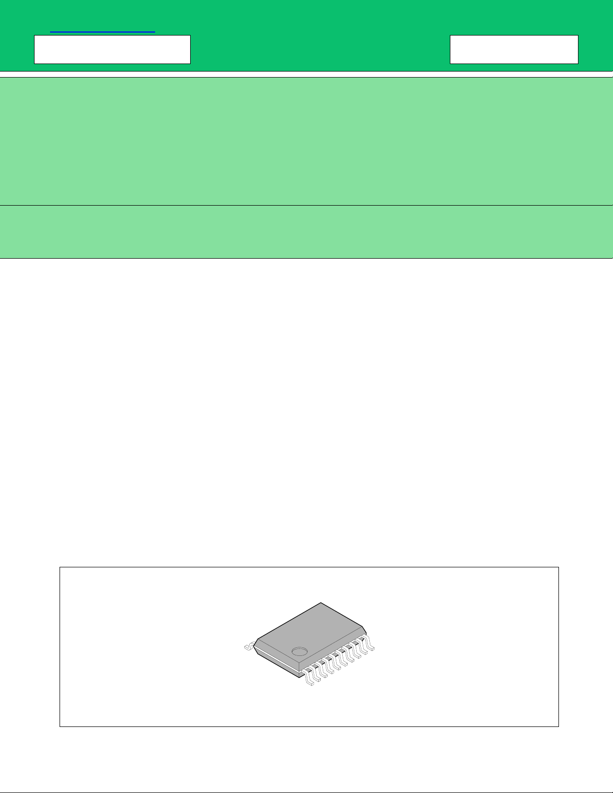
PACKAGE
■
20-pin Plastic SSOP
(FPT-20P-M03)

MB90097
(Continued)
• Font configuration: 12 × 18 dots (font ROM configuration)
Capable of specifying the horizontal and vertical sizes of characters to be displayed.
• One of the following three horizontal sizes (S, M, L) can be set for each character:
S size : 6 dots
M size : 9 dots
L size : 12 dots
• Either of the following two vertical sizes (HA, HB) can be set for each line.
HA : 18 dots
HB : 12 dots
• Display modes: Character trimming Enabled/Disabled (Set for each line)
Character background None/Solid-fill/Shaded background (concaved)/Shaded
background (convexed) (Set for each line)
Horizontal character merge/independent display with
shaded background (Set for each character)
Vertical line merge/independent display with shaded
background (Set for each line)
Character background extended display ON/OFF for line
spacings (Set for each line)
Line background None/Solid-fill/Shaded background (concaved)/Shaded
background (convexed) (Set for each line)
(Display extended to the left and right margins of the screen
and to the line spacing)
Character enlargement: Four types supported: Normal, Double width, Double height,
Enlarged display dot interpolation function (Set for each line)
• Character screen display position control:
Horizontal display position Control in 2-dot units (movable through the entire screen)
Vertical display position Control in 2-dot units (movable through the entire screen)
Line spacing control Control in 1-dot units (Set between 0 to 7 dots for each
line; Displayed simultaneously at two areas above and
below the line.)
• Sprite character control:
Sprite character display OFF/ON
Sprite character types 256 types (character codes: 000
Sprite character trimming Enabled/Disabled
Sprite character configuration Two types: 1 character/Stack of 2 characters
Sprite character horizontal display position Control in 1-dot units (movable through the entire screen)
Sprite character vertical display position Control in 1-dot units (movable through the entire screen)
Double width × double height
(Set for each line)
H to 0FFH)
(Continued)
2

(Continued)
• Screen background control: Screen background color OFF/ON
Display colors Character color: 16 colors (Set for each character)
Character trimming color: 16 colors (Set for each line)
Character background color: 16 colors (Set for each character) *
Line background color: 16 colors (Set for each line)
Screen background color: 16 colors
Sprite character color: 16 colors
Sprite character trimming color: 16 colors
Shaded background frame highlight color: 16 colors
Shaded background frame shadow color: 16 colors
*: Transparent (Displaying the lower-layer color) when the character
background color (color code) = “0”
• Display signal output: Color signal output: 4 bits (Supporting 16 colors)
Display period signals: 3 channels (Output selector circuit provid ed)
• External interface: 16-bit serial inputs
• Chip select
• Serial clock
• Serial data
•Package: SSOP-20
• Supply voltage: 3.3 V
MB90097
3
MB90097
PIN ASSIGNMENT
■
(Top view)
SCLK
CS
SIN
RESET
V
SDR
XD
EXD
TEST
GND
1
2
3
4
5
DD
6
7
8
9
10
(FPT-20P-M03)
20
19
18
17
16
15
14
13
12
11
HSYNC
VSYNC
VC0
VC1
VC2
BLKA
VC3
BLKB
TESTO
BLKC
4
PIN DESCRIPTIONS
■
Pin no. Pin name I/O Function
1 SCLK I Shift clock input pin for serial transfer
This pin has an internal pull-up resistor.
MB90097
2CS
3 SIN I Serial data input pin
4 RESET
5V
6 SDR I Data input direction select pin for serial transfer
7
8
9 TEST I LSI test input pin
10 GND — Ground pin
20 HSYNC
19 VSYNC I Vertical sync signal input pin
18
17
16
14
DD — + 3 V power supply pin
XD
EXD
VC0
VC1
VC2
VC3
I Chip select pin
This pin inputs a Low level signal for serial transfer.
The pin has an internal pull-up resistor.
This pin has an internal pull-up resistor.
I Reset input pin
This pin inputs a Low level signal when turning the power on.
This pin inputs the Low level signal in the LSB-first transfer mode for data
input; it inputs the High level signal in the MSB-first transfer mode.
OIExternal circuit pins for display dot clock generator
Connect these pins to external “L” and “C” to form an LC oscillator circuit.
For external input of a display dot clock, input the clock signal to the EXD
pin and leave the XD pin open.
Input the Low level signal during normal use.
I Horizontal sync signal input pin
O
O
Color code signal output pin
O
O
15 BLKA O Display period signal output pin for output channel A
13 BLKB O Display period signal output pin for output channel B
11 BLKC O Display period signal output pin for output channel C
12 TESTO O LSI test output pin
Leave this pin open (unconnected) during normal use.
5
MB90097
ABSOLUTE MAXIMUM RATINGS
■
Parameter Symbol
(VGND = 0 V)
Rating
Unit Remarks
Min. Max.
Power supply voltage V
DD VGND – 0.3 VGND + 4.5 V
Input voltage VIN VGND – 0.3 VDD + 0.3 V
Output voltage V
OUT VGND – 0.3 VDD + 0.3 V
Power consumption Pd — 100 mW
Operating temperature Ta – 40 + 85 °C
Storage temperature Tstg – 55 + 150 °C
WARNING: Semiconductor devices can be permanently damaged by application of stress (voltage, current,
temperature, etc.) in excess of absolute maximum ratings. Do not exceed these ratings.
RECOMMENDED OPERATING CONDITIONS
■
(VGND = 0 V)
Value
Parameter Symbol
Unit Remarks
Min. Max.
Power supply voltage V
“H” level input voltage V
“L” level input voltage V
DD 3.0 3.6 V
IHS 0.8 × VDD VDD + 0.3 V
ILS VGND 0.2 × VDD V
Operating temperature Ta – 40 + 85 °C
WARNING: The recommended operating conditions are required in order to ensure the normal operation of the
semiconductor device. All of the device's electrical characteristics are warranted when the device is
operated within these ranges.
Always use semiconductor devices within their recommended operating condition ranges. Operation
outside these ranges may adversely affect reliability and could result in device failure.
No warranty is made with respect to uses, operating conditions, or combinations not represented on
the data sheet. Users considering application outside the listed conditions are advised to contact their
FUJITSU representatives beforehand.
6
ELECTRICAL CHARACTERISTICS
■
1. DC Characteristics
Parameter Symbol Pin name Conditions
MB90097
(VGND = 0 V, Ta = – 40°C to + 85°C)
Value
Unit
Min. Typ. Max.
“H” level output voltage 1
“L” level output voltage 1 V
“H” level output voltage 2 V
“L” level output voltage 2 V
“H” level input current
“L” level input current I
PULL-UP resistance R
Power supply current I
Input capacitance C
VC3
VOH1
VC2
VC1
VC0
BLKC
OL1
BLKB
BLKA
OH2
XD
OL2
SDR
IIH
HSYNC
VSYNC
EXD
IL
TEST
RESET
SIN
PULL
SCLK
CS
CC VDD
except V
GND
V
DD = 3.0 V
IOH = – 4.0 mA
VDD = 3.0 V
I
OL = 4.0 mA
V
DD = 3.0 V
IOH = – 0.5 mA
VDD = 3.0 V
I
OL = 0.5 mA
VDD = 3.3 V
V
IH = VDD
VDD = 3.3 V
V
IL = 0 V
DD – 0.5 — — V
V
——0.4V
DD – 0.5 — — V
V
——0.4V
——– 10µA
——10µA
VDD = 3.3 V 20 — 110 kΩ
VDD = 3.0 V
fDC = 8 MHZ
V
f
DD,
DD = 3.6 V
DC = 8 MHZ
—4 6mA
—5 7mA
—10—pF
7
MB90097
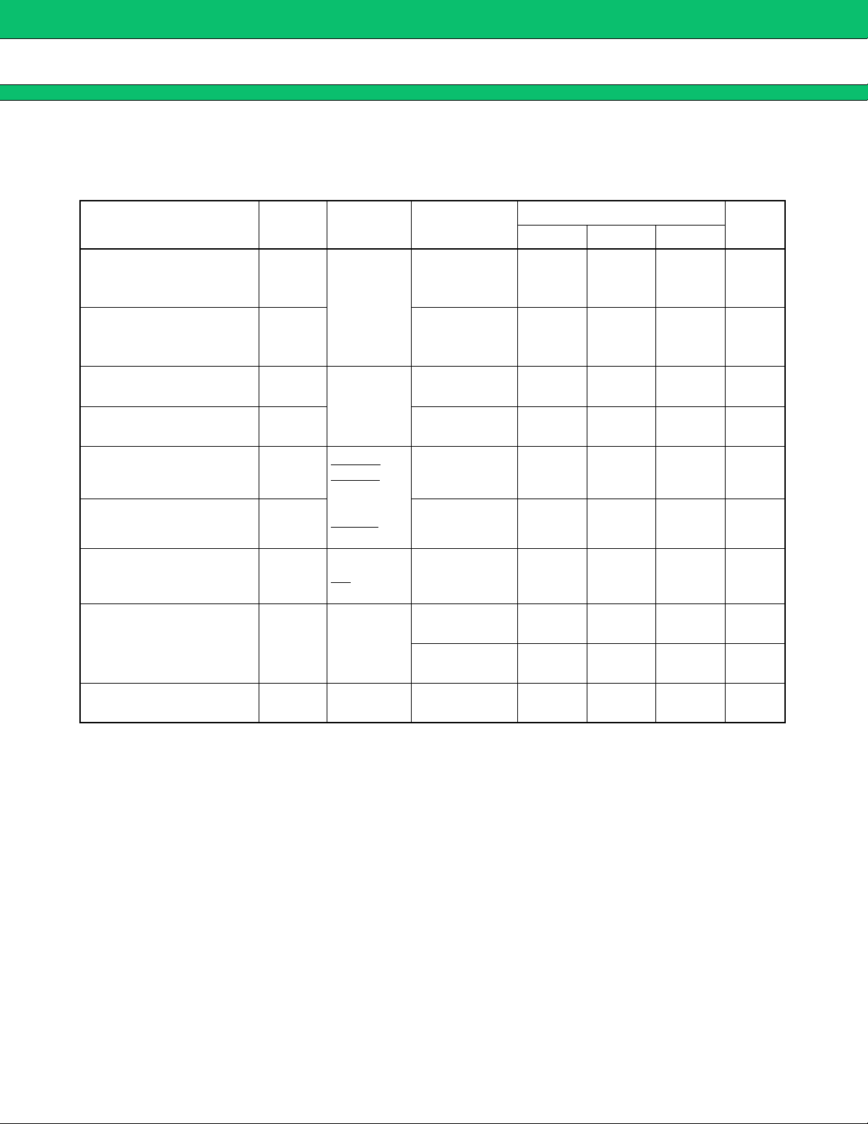
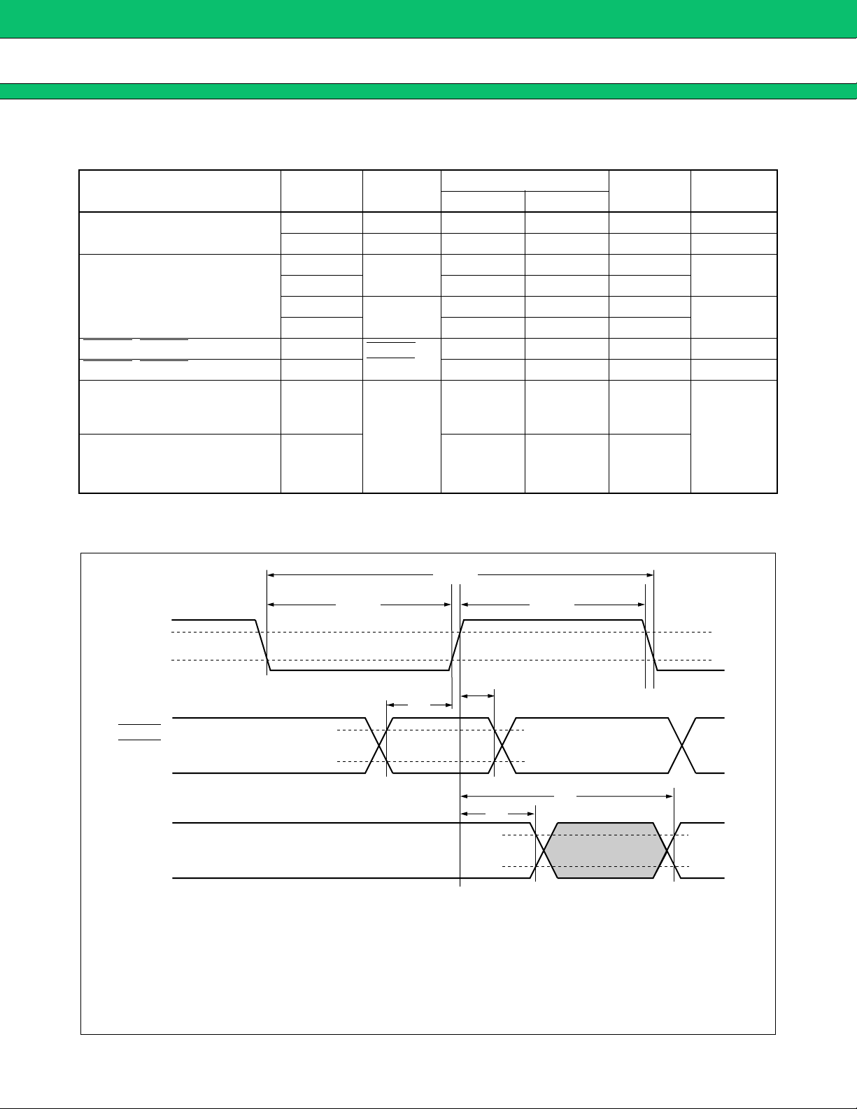
2. AC Characteristics
(1) Serial input timings
(V
DD = 3.0 V to 3.6 V, VGND = 0 V, Ta = – 40°C to + 85°C)
Parameter Symbol Pin name
Unit
Min. Max.
Value
Shift clock cycle time t
Shift clock pulse width
Shift clock signal rise/fall time
CYC SCLK 250 — ns
WCH
t
100 — ns
SCLK
WCL 100 — ns
t
CR
t
—200ns
SCLK
CF —200ns
t
Shift clock start time tSS SCLK 100 — ns
Data setup time t
Data hold time t
SU SIN 100 — ns
H SIN 50 — ns
Chip select end time tEC CS 100 — ns
Chip select signal rise/fall time
CS
0.8 VDD
0.2 VDD
CRC
t
CS
t
CFC —200ns
—200ns
0.8 VDD
0.2 VDD
SCLK
SIN
tCFC
tSS
tCR tCR
tSU
tWCH
tH
tCYC
tWCL
tCF
0.8 VDD
0.2 VDD
tCRC
tEC
0.8 VDD
0.2 VDD
8
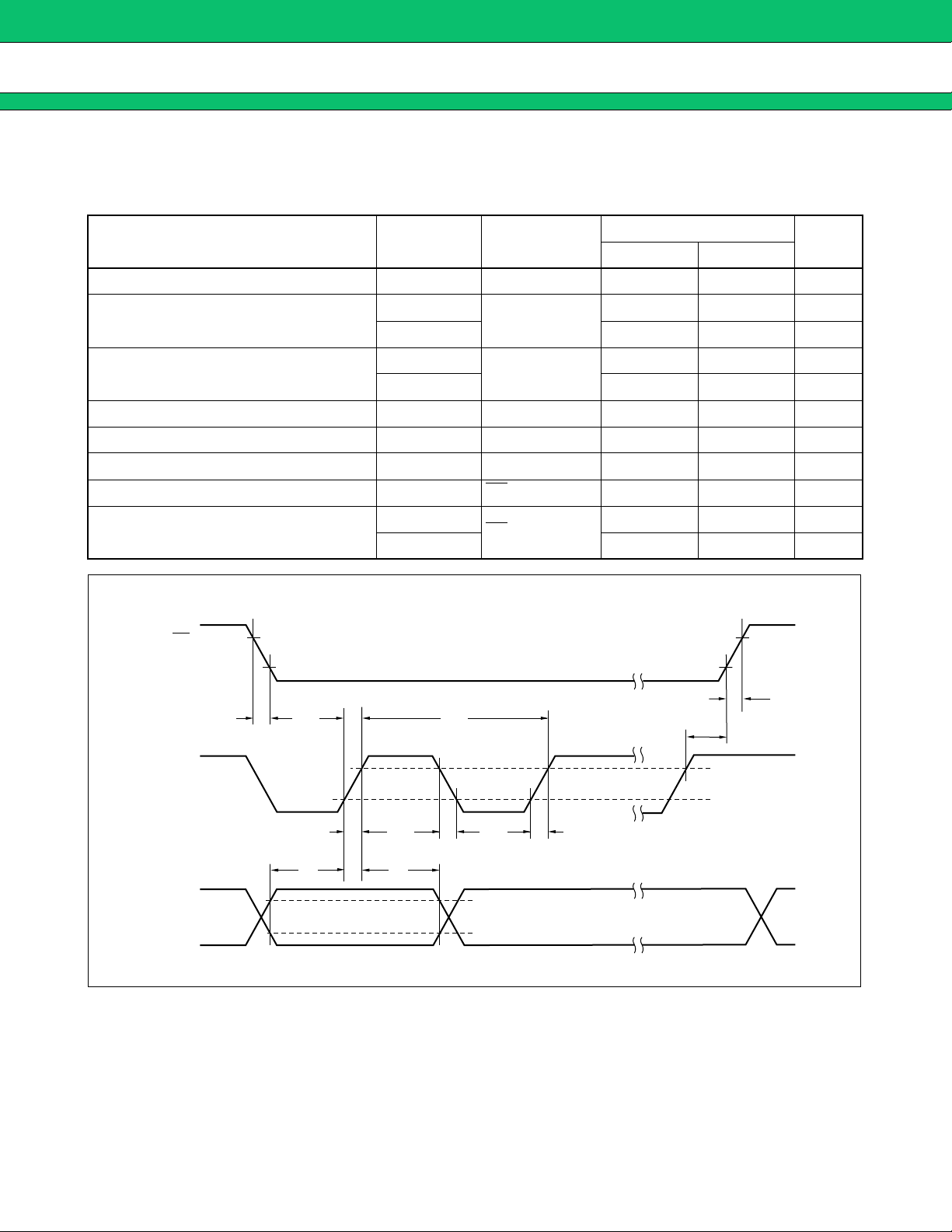
(2) Vertical and horizontal sync signal input timings
MB90097
(V
DD = 3.0 V to 3.6 V, VGND = 0 V, Ta = – 40°C to + 85°C)
Parameter Symbol Pin name
Unit
Min. Max.
Value
Horizontal sync signal rise time t
HR
— 200 ns
HSYNC
Horizontal sync signal fall time tHF — 200 ns
Vertical sync signal rise time t
VR
— 200 ns
VSYNC
Vertical sync signal fall time t
Horizontal sync signal pulse width
*1
VF — 200 ns
18 — Dot clock
tWH HSYNC
—6µs
*2
Vertical sync signal detection setup time
Vertical sync signal detection hold time t
tVS VSYNC 4 1H – 4 Dot clock
VH VSYNC 220H
*1: During the horizontal sync signal pulse period, the MB90097 stops its internal operation, disabling writing to
the internal VRAM. Therefore, set the horizontal sync signal pulse width and VRAM write cycle (command 2 or
command 4 issuance cycle) to ensure that: horizontal sync signal pulse width < VRAM write cycle.
*2: Do not change the vertical sync signal (detection edge) in the vicinity of the horizontal sync signal edge of
vertical sync signal detection. Otherwise, it results in a deflection in the display when the sync signal fluctuates.
(1) VSYNC: Leading-edge operation
HSYNC: VSYNC detection at the trailing edge
VSYNC
HSYNC
0.8 VDD
0.8 VDD
tVF
tVS
0.2 VDD
tHF tHR
tWH
0.2 VDD
0.2 VDD
tVH
0.8 VDD
tVR
0.8 VDD
0.2 VDD
Note: The above diagrams assume that sync signal input control (SIX bit) of I/O pin control (command 13-0) has
been set to negative logic (0). The H and L levels are inverted if it has been set to positive logic.
(Continued)
9
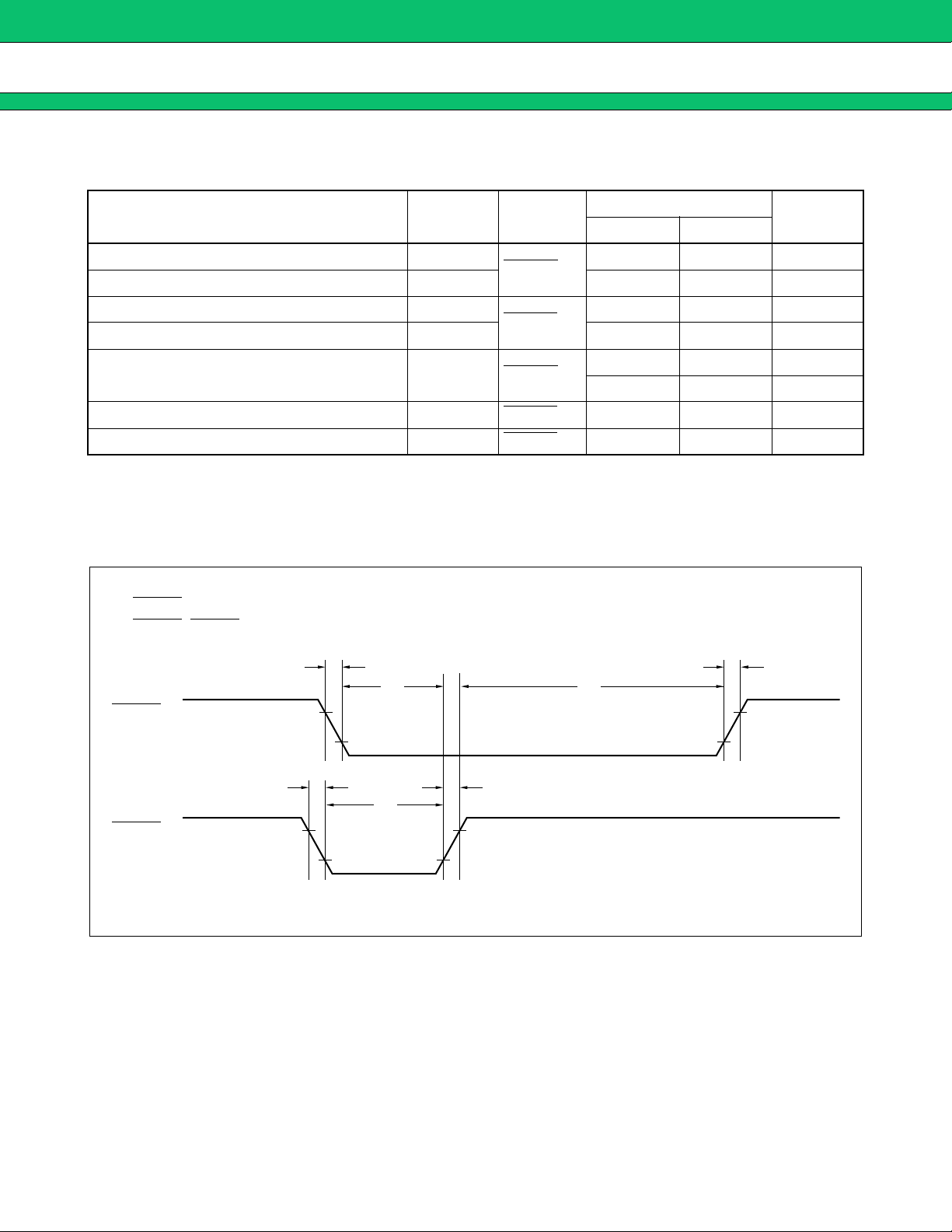
MB90097
(Continued)
(2) VSYNC: Trailing-edge operation
HSYNC: VSYNC detection at the trailing edge
VSYNC
HSYNC
0.2 VDD
0.8 VDD
0.8 VDD
tHF tHR
0.2 VDD
(3) VSYNC: Leading-edge operation
HSYNC: VSYNC detection at the leading edge
VSYNC
0.8 VDD
0.2 VDD
tVR
tVF
tWH
tVS
tVS
tVF
tVH
0.8 VDD
0.2 VDD
0.8 VDD
0.2 VDD
tVR
tVH
0.8 VDD
0.2 VDD
tHF tHR
tWH
HSYNC
(4) VSYNC: Trailing-edge operation
HSYNC: VSYNC detection at the leading edge
VSYNC
HSYNC
10
0.2 VDD
tVR
0.8 VDD
0.8 VDD
tVS
0.8 VDD
0.2 VDD
tVH
tHF tHR
tWH
0.2 VDD
0.8 VDD
0.2 VDD
tVF
0.8 VDD
0.2 VDD
0.8 V DD
0.2 VDD
(3) Dot clock input timing
Parameter Symbol Pin name
Dot clock cycle time
Dot clock pulse time
HSYNC
HSYNC
, VSYNC setup time tDS
, VSYNC hold time tDH 0—ns*3
Data output delay time 1
Data output delay time 2 t
MB90097
(V
DD = 3.0 V to 3.6 V, VGND = 0 V, Ta = – 40°C to + 85°C)
Value
Min. Max.
DCYC1 EXD 112 166 ns *1
t
t
DCYC2 EXD 56 83 ns *2
t
DWH1
DWL1 48 — ns
t
t
DWH2
t
DWL2 24 — ns
EXD
EXD
HSYNC
48 — ns
24 — ns
13 — ns *3
VSYNC
VC3,
tDD1
VC2,
7t
DD2 ns
VC1,
VC0,
BLKA,
DD2 tDD1 45 ns
BLKB,
BLKC
Unit Remarks
*1
*2
*3
*1: Assumes a dot clock LC oscillator circuit or external dot clock input.
*2: Assumes frequency-doubled external dot clock input.
*3: Assumes dot clock external input.
tDCYC1, 2
tDWL1, 2
EXD input
tDH
tDS
HSYNC
VSYNC
Inputs
tDD1
Data output
AC measurement conditions
C = 70 pF
t
r = 5 ns
tf = 5 ns
V
OH = 0.8 VDD
VOL = 0.2 VDD
VIH = 0.8 VDD
VIL = 0.2 VDD
Note: Applicable only when the MB90097 is operating with external dot clock input (not applicable with the LC oscillator circuit).
Previous
data
tDWH1, 2
0.8 VDD
0.2 VDD
tDD2
Undefined period Valid data
0.8 VDD
0.2 VDD
0.8 VDD
0.2 VDD
11
MB90097
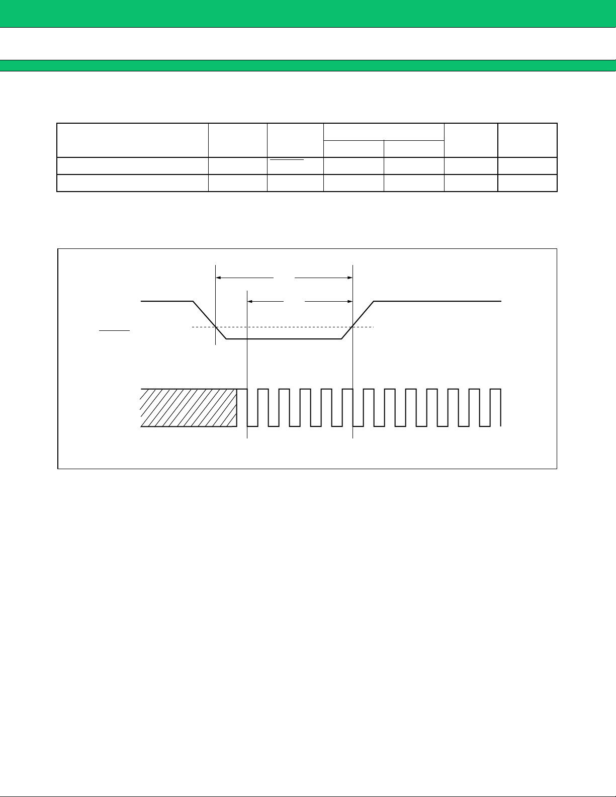
(4) Reset input timing
(V
DD = 3.0 V to 3.6 V, VGND = 0 V, Ta = – 40°C to + 85°C)
Parameter Symbol Pin name
Unit Remarks
Min. Max.
Value
Reset pulse width t
WRST RESET 1—µs
Clock input time tWRSD EXD 5 — Dot clock Note
Note: To feed the EXD pin with the dot clock, it is necessary to input the clock during RESEST. Configuring LC
oscillator circuit using the external L and C will eliminate this need because it will automatically oscillate.
t WRST
t WRSD
0.2 V DD
RESET
EXD
12
MB90097
COMMAND LIST
■
1. Display Control Commands
Command
no.
0
1
2
3
4
5-00
5-01
5-02
5-2
5-3
6-1
7-3
8-0
8-1
9-0
9-1
11-0
11-2 Dot clock control 1 1011 100000000DC2DC1DC0
13-0 I/O pin control 1101 0 0 VVE VHE HE 0 SIX 0 0 0 DBX DCX
13-1
13-2
Function
VRAM write
address setting
Character data
setting 1
Character data
setting 2
Line control data
setting 1
Line control data
setting 2
Screen output
control 1A
Screen output
control 1B
Screen output
control 1C
Vertical display
position control
Horizontal display
position control
Shaded
background frame
color control
Screen
background
control
Sprite character
control 1
Sprite character
control 2
Sprite character
control 4
Sprite character
control 5
Screen extension
control
Horizontal
blanking control 1
Horizontal
blanking control 2
15 to 1211109876543210
0000 AY3 AY2 AY1 AY0 FL 0 0 AX4 AX3 AX2 AX1 AX0
0001 MS1 MS0 MM1 MM0 MB3 MB2 MB1 MB0 MC3 MC2 MC1 MC0
0010 MR MO1 MO0 M8 M7 M6 M5 M4 M3 M2 M1 M0
0011 LHS LW2 LW1 LW0 LFD LFC LFB LFA LF3 LF2 LF1 LF0
0100 LDS LGS LG1 LG0 LD LE LM1 LM0 L3 L2 L1 L0
0101 0000SDSUDS0DSP0OA2OA1OA0
0101 0001SOBBGBBLB00OB2OB1OB0
0101 0010SOCBGCBLC00OC2OC1OC0
0101 1 0 0 Y8 Y7 Y6 Y5 Y4 Y3 Y2 Y1 Y0
0101 1 1 0 X8 X7 X6 X5 X4 X3 X2 X1 X0
0110 0100BH3BH2BH1BH0BS3BS2BS1BS0
0111 11000000U3U2U1U0
1000 0 0 SFB SFA SF3 SF2 SF1 SF0 SC3 SC2 SC1 SC0
1000 0 1 SD1 SD0 SM7 SM6 SM5 SM4 SM3 SM2 SM1 SM0
1001 0 0 SY9 SY8 SY7 SY6 SY5 SY4 SY3 SY2 SY1 SY0
1001 1 0 SX9 SX8 SX7 SX6 SX5 SX4 SX3 SX2 SX1 SX0
1011 00000EG0000000
1101 010000BB5BB4BB3BB2BB1BB0
1101 1 0 0 BF8 BF7 BF6 BF5 BF4 BF3 BF2 BF1 BF0
Command code/data
13
MB90097
g
2. Command Description
• Command 0 (VRAM write address setting)
Command 0 sets the write address in VRAM and controls execution of “VRAM fill.”
The sets the write address by specifying the row and column addresses.
VRAM fill is activated by executing command 2 (character data setting 2).
15
14 13 12 11 10 9 8 7 6 5 4 3 2 1 0
0
0 0 0 AY3 AY2 AY1 AY0 FL 0 0 AX4 AX3 AX2 AX1 AX0
AY3 to AY0: Row address
(0 to B
H)
AX4 to AX0: Column address
(0 to 1BH)
FL: VRAM fill control
(0: OFF, 1: ON)
• Command 1 (Character data setting 1)
Command 1 sets character data.
Executing command 2 (character data setting 2) sets VRAM to reflect it on the screen.
15
14 13 12 11 10 9 8 7 6 5 4 3 2 1 0
0
0 0 1 MS1 MS0 MM1 MM0 MB3 MB2 MB1 MB0 MC3 MC2 MC1 MC0
MC3 to MC0: Character color
(From among 16 colors)
MB3 to MB0: Character background color
(From among 16 colors)
MM1, MM0: Character background control
(0, 0: OFF)
(0, 1: Solid-fill display)
(1, 0: Concaved, shaded background)
(1, 1: Convexed, shaded back
round)
MS1, MS0: Character horizontal size control
(0, 0: S size, 6 dots)
(0, 1: M size, 9 dots)
(1, 0: L size, 12 dots)
(1, 1: Setting prohibited)
• Command 2 (Character data setting 2)
Command 2 writes additional character data to the location in VRAM specified by command 0 (VRAM write
address setting 1), along with the character data set by command 1 (character data setting 1).
The VRAM write address is incremented automatically after execution of command 2.
14
15
14 13 12 11 10 9 8 7 6 5 4 3 2 1 0
0
0 1 0 MR MO1 MO0 M8 M7 M6 M5 M4 M3 M2 M1 M0
MR: Shaded background succeeding character merge control
(0: Disables succeeding character merge display.)
(1: Enables succeeding character merge display.)
M8 to M0: Character code
MO1, MO0: Character output control
• Command 3 (Line control data setting 1)
)
g
Command 3 sets line control data.
Executing command 4 (line control data setting 2) sets VRAM to reflect it on the screen.
MB90097
15
LHS: Line character vertical size type control
(0: Character vertical size A)
(1: Character vertical size B)
LW2 to LW0: Line spacing control
(0 to 7 dots in 1-dot units)
LF3 to LF0: Trimming color
(From among 16 colors)
14 13 12 11 10 9 8 7 6 5 4 3 2 1 0
0
0 1 1 LHS LW2 LW1 LW0 LFD LFC LFB LFA LF3 LF2 LF1 LF0
LFD, LFC: Trimming output control
(0, 0: All OFF)
(0, 1: Trimming ON for character with no character background)
(1, 0: Trimming ON for solid-filled character with no character background
(1, 1: All ON)
LFB, LFA: Trimming control
(0, 0: Trimming OFF)
(0, 1: Reserved (Setting prohibited))
(1, 0: Reserved (Setting prohibited))
(1, 1: Eight-direction trimming)
• Command 4 (Line control data setting 2)
Command 4 writes additional line control data to the row address in line RAM specified by command 0
(VRAM write address setting), along with the line control data set by command 3 (line control data setting1).
Executing this command will not alter the VRAM write address.
15
14 13 12 11 10 9 8 7 6 5 4 3 2 1 0
0
1 0 0 LDS LGS LG1 LG0 LD LE LM1 LM0 L3 L2 L1 L0
LDS: Line character output control
(Control of character + trimming + character background)
(0: OFF, 1: ON)
LGS: Line enlargement interpolation control
(0: OFF, 1: ON)
LG1, LG0: Line enlargement control
(0, 0: Normal)
(0, 1: Double width)
(1, 0: Double height)
(1, 1: Double width × double height)
LE: Character background extension control
(0: Normal, 1: Extended)
LD: Shaded background succeeding line merge control
(0: Independent, 1: Merge with the next line)
LM1, LM0: Line background control
(0, 0: OFF)
(0, 1: Solid-fill display)
(1, 0: Concaved, shaded display)
(1, 1: Convexed, shaded display)
L3 to L0: Line background color
(From amon
16 colors)
• Command 5-00 (Screen output control 1A)
Command 5-00 controls screen display output.
15
14 13 12 11 10 9 8 7 6 5 4 3 2 1 0
0
1 0 1 0 0 0 0 SDS UDS 0 DSP 0 OA2 OA1 OA0
SDS: Sprite character output control
(0: OFF, 1: ON)*
UDS: Screen background output control
(0: OFF, 1: ON)*
DSP: Display output control
(Control of character + trimming + character background +
line background)
(0: OFF, 1: ON)*
*: The low level input to the RESET pin initializes the SDS, UDS, and DSP bits to 0.
OA2 to OA0: Output-A character control
(From among eight types)
15

MB90097
• Command 5-01 (Screen output control 1B)
Command 5-01 controls output-B screen display output.
15
14 13 12 11 10 9 8 7 6 5 4 3 2 1 0
0
1 0 1 0 0 0 1 SOB BGB BLB 0 0 OB2 OB1 OB0
SOB: Output-B sprite character output control
(0: OFF, 1: ON)
BGB: Output-B screen background output control
(0: OFF, 1: ON)
BLB : Output-B line background output control
(0: OFF, 1: ON)
OB2 to OB0: Output-B character control
(From among eight types)
• Command 5-02 (Screen output control 1C)
Command 5-02 controls output-C screen display output.
15
14 13 12 11 10 9 8 7 6 5 4 3 2 1 0
0
1 0 1 0 0 1 0 SOC BGC BLC 0 0 OC2 OC1 OC0
SOC: Output-C sprite character output control
(0: OFF, 1: ON)
BGC: Output-C screen background output control
(0: OFF, 1: ON)
BLC : Output-C line background output control
(0: OFF, 1: ON)
OC2 to OC0: Output-C character control
(From among eight types)
• Command 5-2 (Vertical display position control)
This command controls the vertical display position of the screen.
15
14131211109 876543210
16
0
1 0 1 1 0 0 Y8 Y7 Y6 Y5 Y4 Y3 Y2 Y1 Y0
Y8 to Y0: Vertical display position control
(0 to 1022 in 2-dot units)
• Command 5-3 (Horizontal display position control)
This command controls the horizontal display position of the screen.
15
14131211109 876543210
0
1 0 1 1 1 0 X8 X7 X6 X5 X4 X3 X2 X1 X0
X8 to X0: Horizontal display position control
(0 to 1022 in 2-dot units)
• Command 6-1 (Shaded background frame color control)
Command 6-1 controls the frame color of a shaded background.
15
14131211109 876543210
0
1 1 0 0 1 0 0 BH3 BH2 BH1 BH0 BS3 BS2 BS1 BS0
BH3 to BH0: Shaded background frame highlight color
(From among 16 colors)
BS3 to BS0: Shaded background frame shadow color
(From among 16 colors)
• Command 7-3 (Screen background control)
Command 7-3 controls the screen background color.
15
14131211109 876543210
0
11111000000U3U2U1U0
U3 to U0: Screen background color
(From among 16 colors)
MB90097
• Command 8-0 (Sprite character control 1)
This command controls sprite characters.
15
14131211109 876543210
1
0 0 0 0 0 SFB SFA SF3 SF2 SF1 SF0 SC3 SC2 SC1 SC0
SFB, SFA: Sprite character trimming control
(0, 0: Trimming OFF)
(0, 1: Reserved)
(1, 0: Reserved)
(1, 1: Eight-direction trimming)
• Command 8-1 (Sprite character control 2)
Command 8-1 controls sprite characters.
15
14131211109 876543210
1
0 0 0 0 1 SD1 SD0 SM7 SM6 SM5 SM4 SM3 SM2 SM1 SM0
SD1, SD0: Sprite character configuration control
(0, 0: 1 character)
(0, 1: Reserved (Setting prohibited))
(1, 0: Stack of 2 characters)
(1, 1: Reserved (Setting prohibited))
SF3 to SF0 : Sprite character trimming color
(From among 16 colors)
SC3 to SC0: Sprite character color
(From among 16 colors)
SM7 to SM0: Sprite character code
(000
H to 0FFH for 256 different characters)
17
MB90097
• Command 9-0 (Sprite character control 4)
Command 9-0 controls sprite characters.
15
14131211109 876543210
1
0 0 1 0 0 SY9 SY8 SY7 SY6 SY5 SY4 SY3 SY2 SY1 SY0
• Command 9-1 (Sprite character control 5)
This command controls sprite characters.
15
14131211109 876543210
1
0 0 1 1 0 SX9 SX8 SX7 SX6 SX5 SX4 SX3 SX2 SX1 SX0
SY9 to SY0: Sprite character vertical display position control
(0 to 1023 in 1-dot units)
SX9 to SX0: Sprite character horizontal display position control
(0 to 1023 in 1-dot units)
• Command 11-0 (Screen extension control)
(Reserved)
15
141312111098 76543210
1
01100 000EG0000000
• Command 11-2 (Dot clock control 1)
Command 11-2 controls the dot clock.
15
14131211109 876543210
1
0 1 1 1 0 0 0 0 0 0 0 0 DC2 DC1 DC0
EG0: (Reserved)
(0: Normal)
(1: Reserved (Setting prohibited))
*
: Set the EG0 bit to “0”.
DC2 to DC0: Dot clock selection control
(0, 0, 0: LC oscillation)
(0, 1, 0: External dot clock input)
(0, 1, 1: Frequency-doubled external dot clock input)
*
18
• Command 13-0 (I/O pin control)
Command 13-0 controls input/output pins.
15
14131211109 876543210
1
1 0 1 0 0 VVE VHE HE 0 SIX 0 0 0 DBX DCX
MB90097
VVE: Edge selection for vertical synchronization detection
(0: Leading edge, 1: Trailing edge)
VHE: HSYNC edge selection for vertical synchronization detection
(0: Leading edge, 1: Trailing edge)
HE: Edge selection for horizontal synchronization operation
(0: Trailing edge, 1: Leading edge)
*: The low level input to the RESET pin initializes the DCX and DBX bits to 0.
SIX : Logic control for sync signal input
(0: Negative logic, 1: Positive logic)
DCX: Logic control for display color signal output
(0: Positive logic, 1: Negative logic)*
DBX: Logic control for display output period signal output
(0: Positive logic, 1: Negative logic)*
• Command 13-1 (Horizontal blanking control 1)
Command 13-1 controls horizontal blanking (back porch).
15
14131211109 876543210
1
1 0 1 0 1 0 0 0 0 BB5 BB4 BB3 BB2 BB1 BB0
BB5 to BB0: Back porch control
(0 to 126 in 2-dot units)
• Command 13-2 (Horizontal blanking control 2)
Command 13-2 controls horizontal blanking (front porch).
15
14131211109 876543210
1
1 0 1 1 0 0 BF8 BF7 BF6 BF5 BF4 BF3 BF2 BF1 BF0
BF8 to BF0: Front porch control
(0 to 1022 in 2-dot units)
19

MB90097
3. Notes on Issuing Commands
This section summarizes notes on issuing commands.
(1) Initialization
The MB90097 enters the display-off state (*1) upon reset input (input of a LOW-level signal to the RESET pin).
The contents of VRAM (character RAM and line RAM) are not initialized then (undefined immediately after the
power supply is turned on).
When the MB90097 is released from the reset input, issue the following commands to initialize control
operation:
• Dot clock control 1 (Command 11-2)
• I/O pin control (Command 13-0)
After that, set all of other command data and the contents of VRAM.
(VRAM setting requires normal dot clock and sync signal inputs.)
*1: The reset input initializes control bits to 0 as shown below
Screen output control 1A (command 5-00) SDS = 0 Sprite OFF
UDS = 0 Screen background OFF
DSP = 0 Character, character background, line
background OFF
I/O pin control (command 13-0) DCX = 0 Sets the VC0, VC1, VC2, and VC3 pins to
positive logic output.
DBX = 0 Sets the BLKA, BLKB, and BLKC pins to positive
logic output.
(2) Command refresh
Command data to the MB90097 and the contents of internal VRAM remain held as long as the MB90097 is
powered. If the serial control, sync, and dot clock signals are affected by external noise, however, they may
become abnormal signals, preventing the internal registers and VRAM from being set normally. You should
therefore refresh all of command data and VRAM data periodically to restore them from the abnormal state.
(3) Command issuance timing
When a VRAM write command, such as a character data setting or line control data setting command, or any
other control command is issued, the command is executed immediately, reflecting the result (command setting)
on the screen. When such a command is issued during a display period, the display in the relevant field may
involve transient distortion. To prevent this, you should issue the command during the vertical blanking interval.
Also, a restriction on the internal circuit configuration may cause deviation of the display position in the first
display field when the DSP, SDS, or UDS control bit of command 5-00 (screen output control 1A) is set from
OFF to ON. To prevent this, you should issue command 5-00 within the 2H period after the leading edge of the
V sync signal.
20

DISPLAY FUNCTIONS
■
1. Screen Configuration
1. 1 Screen Elements
The display screen provided by the MB90097 consists of a pile of display screen elements.
Display screen element name Display configuration Display position control
Top layer
Sprite character (+ trimming)
Character (+ trimming) 28 characters × 12 lines Horizontal/vertical: 2-dot units
1 (Maximum of 2 × 2
characters)
Horizontal/vertical: 1-dot units
MB90097
Character background 28 characters × 12 lines
Line background 12 lines
Bottom layer
Screen background
• Screen configuration drawing
Input image
Screen background (Screen background color)
Line 0 Line background (Line background color)
Line 1
Line 2
Line 3
Line 4
Line 5
Line 6
Line 7
Line 8
Line 9
Line 10
Line 11
Full screen display in single
color
Character background
(Character background color)
Character + trimming
← Sprite character + trimming
(Controlled simultaneously with
the character)
(Controlled simultaneously with
the character)
(None)
Note: When a character is displayed on a line, the display of the shaded background shadow frame
for the line background overrides the character display.
The display of the shaded background shadow frame for the character background overrides
the character display and the shaded background shadow frame for the line background.
21

MB90097
y
1. 2 Screen Display Modes
Display screen
element name
Screen
background
Line
background
Character
background
Display mode
Undisplay
Display
Undisplay
Solid-fill display
Shaded background concaved display
Shaded background convexed display Merge
Undisplay
Solid-fill display
Shaded
background
concaved
display
Shaded
background
convexed
display
Undisplay (blank character (Arbitrarily set))
Shaded
background
succeeding
character
merge
Independent
Merge Merge Extended
Shaded
background
succeeding
line merge
Shaded
background
succeeding
line merge
Independent
Independent
Line spacing (0 to 7
dots)
Character
background
extended
(enabled
with line
spacing)
Normal
Character
Sprite
character
Display
Undisplay
Display
Undisplay
Display for characters with no character
background
Trimming output
control
Consisting of a single character
Consisting of a stack of characters
Display for characters with no character
background or with solid-filled
character background
Display for all characters
Trimming
type
Undispla
Trimming
type
Undisplay
Eight-direction
trimming display
Eightdirection
trimming
display
22

MB90097
1. 3 Screen Output Control
The screen output control commands can control three channels of outputs A, B, and C independently.
Their output enable period signals are output to the BLKA, BLKB, and BLKC pins, respectively.
The output-A, -B, and -C control commands can set the character attribute display to OFF, line background
display, and screen background display arbitrarily based on the basic display screen, allowing three independent
screens to be configured and output.
The layer structure of the output screens exists only on the basic display screen. If the output-A, -B, or -C
control command sets the display of an arbitrary area to OFF, the lower layer cannot be displayed but appears
transparent.
The table below shows the relationships between screen output controls and control command bits.
Basic display screen control Three-channel output controls
Elements to be controlled/Control bit name
(Unit of control)
Output-A control Output-B control Output-C control
Character + trimming + character background +
line background
←←←
DSP (per screen)
Character + trimming + character
background LDS (per line)
Character M8-M0 (per character)
Character trimming
LFD-LFA (per line)
Character background
MM1, MM0 (per character)
Line background LM1, LM0 (per line) ←
Screen background color UDS (per screen) ←
Sprite character SDS (per screen) ←
Sprite character trimming
SFB, SFA (per screen)
←←←
OA2-OA0
(per screen)
×
MO1, MO0
*1
(per character)
←
OB2-OB0
(per screen)
×
MO1, MO0
*1
(per character)
*2
BLB
(per screen)
BGB
(per screen)
*3
SOB
(per screen)
OC2-OC0
(per screen)
×
MO1, MO0
(per character)
*2
BLC
(per screen)
BGC
(per screen)
*3
SOC
(per screen)
*1
*1: If character display is set to OFF with the character/trimming/character background overlapping the line
background or screen background, the corresponding area of the lower layer is not displayed but appears
transparent.
*2: If line background display is set to OFF with the line background overlapping the screen background, the
corresponding area of the screen background is not displayed but appears transparent.
*3: If sprite display is set to OFF with the sprite character/trimming overlapping a character, character background,
line background, or screen background, the corresponding area of the lower layer is not displayed but appears
transparent.
Note: Three-channel output control for each character serves as output control within the character area. When
trimming dots for a character are displayed in part of the area for an adjacent character, the output of the
trimming dots is controlled by the output control of that adjacent character. If there are trimming dots to the
left of the leftmost character on a line, they cannot be controlled by three-channel output control for each
character. In this case, set a blank character at the left end of the line.
When trimming dots are displayed to the right of the rightmost character on a line, they are controlled with
the three-channel output attribute of the rightmost character.
23

MB90097
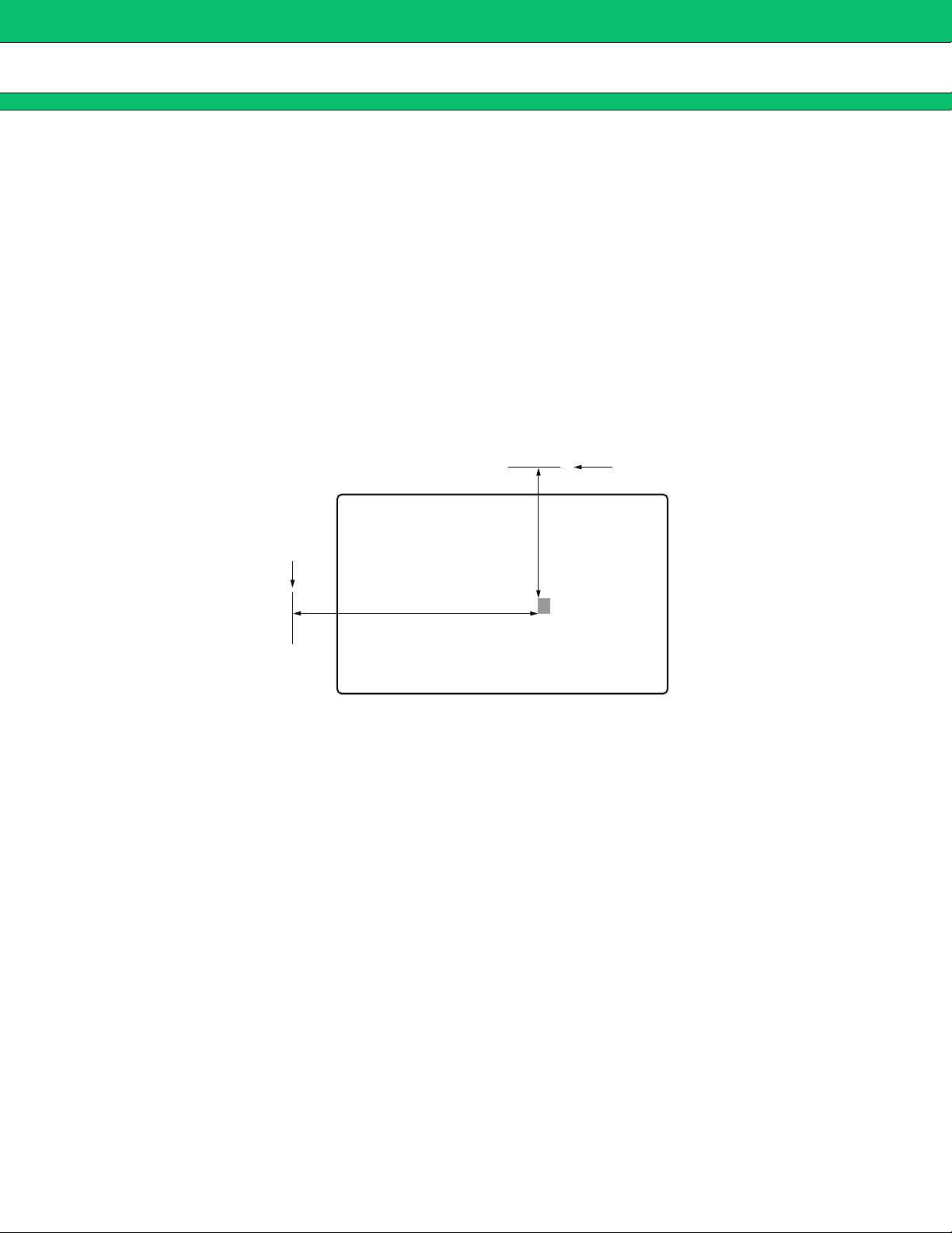
1. 4 Screen Display Position Control
(1) Display position control on the character screen
The MB90097 can simultaneously control the display start positions of a character (or a line of characters),
character trimming, character background, and line background.
• Vertical display position: Vertical display position control (command 5-2), Bits Y8 to Y0
Set the vertical display start position*
The position can be set between 0 and 1022 dots in 2-dot units.
(*1: The actual display position is offset from the set value by several tens of dots
in the positive direction.)
• Horizontal display position: Horizontal display position control (command 5-3), Bits X8 to X0
Set the vertical display start position
The position ca
*
n be set between 0 and 1022 dots in 2-dot units.
(*2: The actual display position is offset from the set value b y sev eral tens of dots
in the positive direction.)
• Line spacing: Line control data setting 1 (command 3), Bits LW2 to LW0
Set the number of dots to specify the height of the areas to be kept above and
below the characters on each line.
The spacing specified by the set value will be kept both above and below the
characters.
The line spacing can be set between 0 and 7 dots in 1-dot units for each line.
(Note: When line double-height display is on, the line spacing is doubled as well.)
VSYNC position*
1
relative to the VSYNC position.
*2
relative to the HSYNC position.
3
HSYNC position*
Line 0
Line 1
Line 2
3
Line spacing
Horizontal
display position
Line spacing
Line spacing
Vertical display position
Character Character Character Character Character Character Character Character Character
Character Character Character Character Character Character Character Character Character
Character Character Character Character Character Character Character Character Character
• • •
• • •
• • •
• • •
• • •
• • •
• • •
• • •
• • •
• • •
• • •
• • •
• • •
• • •
• • •
*3: For the VSYNC position, you can select the leading or trailing edge of the vertical sync signal pulse.
For the HSYNC position, you can select the leading or trailing edge of the horizontal sync signal pulse.
(For details, see Section 3 “Sync Signal Input” of “■ CONTROL FUNCTIONS.”)
24
MB90097
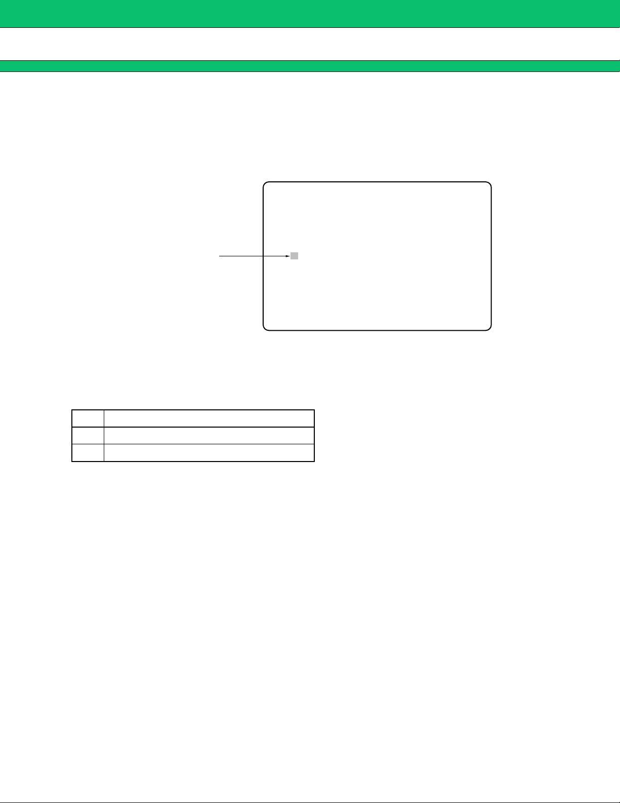
(2) Display position control of sprite characters
The MB90097 can control the display start positions of a sprite character and its trimming.
• Sprite character vertical display position: Sprite character control 4 (command 9-0), Bits SY9 to SY0
Set the vertical display start position*
position.
The position can be set between 0 and 1023 dots in 1-dot units.
(*1: The actual display position is offset from the set value by
several tens of dots in the positive direction.)
• Sprite character horizontal display position: Sprite character control 5 (command 9-1), Bits SX9 to SX0
Set the vertical display start position*
position.
The position can be set between 0 and 1023 dots in 1-dot units.
(*2: The actual display position is offset from the set value by
several tens of dots in the positive direction.)
1
relative to the VSYNC
2
relative to the HSYNC
3
HSYNC position*
3
Sprite character horizontal
display position
VSYNC position*
Sprite character
vertical display
position*
1
Sprite character
*3: For the VSYNC position, you can select the leading or trailing edge of the vertical sync signal pulse.
For the HSYNC position, you can select the leading or trailing edge of the horizontal sync signal pulse.
(For details, see Section 3 “Sync Signal Input” of “■ CONTROL FUNCTIONS.”)
25

MB90097
2. Font ROM Configuration
The font ROM can incorporate 512 characters each made up of 12 × 18 dots.
• All of 512 characters can be set freely by the user.
(Note, however, that the blank character must be set as an arbitrar y character code because even it is not
set by default.)
• The user areas available to sprite characters are from 000
Font ROM
H to 0FFH.
000 H
001 H
002 H
0FE H
0FF H
100 H
101 H
102 H
1FE H
(User area)
(User area)
(User area)
(User area)
(User area)
(User area)
(User area)
(User area)
(User area)
Areas available
to sprite characters
12 dots
18 dots
26
1FF H
↑
Character code
(User area)
(Character configuration example)

MB90097
3. Display Memory (VRAM) Configuration
The display memory (VRAM) consists of the character RAM for setting individual characters and the line RAM
for setting individual lines.
• Character RAM: 28 characters × 12 lines (336 characters in total)
• Line RAM: 12 lines
3. 1 Display Memory and Display Screen
Areas of character RAM and those of line RAM correspond to displayed characters and lines on a one-to-one
basis, respectively.
• Display memory configuration
Character RAM
0
1
2
3
4
5
6
7
Row addresses
8
9
10
11
0123456789012345678901234567
111111111122222222
Column addresses
• Example of display screen configuration (with all characters in normal size)
VRAM row address
0
1
2
3
4
5
6
7
8
9
10
11
Line RAM
VRAM column address
0123456789012345678901234567
111111111122222222
27

MB90097
3. 2 Writing to Display Memory
(1) Writing characters to character RAM
a) Writing a single character
Use the following commands to write data on an arbitrary character to an arbitrary address in character
RAM:
1
*
VRAM write address setting
Character data setting 1
(Command 0)
(Command 1)
Set the row and column addresses.
2
*
Character data setting 2
(Command 2)
Write the character data to character RAM.
(The VRAM write address is incremented after writing to VRAM.)
*1: When writing to consecutive addresses continuously, you can omit this command for the latter character RAM
write.
*2: You can also omit this command if the current character data is the same as the one set by the preceding
“character data setting 1” command.
Note: Normal writing to VRAM requires input of a normal horizontal sync signal. Input of an invalid horizontal sync
signal may cause VRAM write to fail.
Also, you must set the horizontal sync signal pulse width and VRAM write cycle (command 2 or command
4 issuance cycle) such that: horizontal sync signal pulse width < VRAM write cycle.
b) Writing multiple characters collectively (VRAM fill)
Use the following commands to write data on an arbitrary character to an area of character RAM from an
arbitrary address to the last address, filling the area with that data:
VRAM write address setting
Character data setting 1
Character data setting 2
(Command 0)
(Command 1)
(Command 2)
Set the row and column addresses and specify “VRAM fill”.
3
The character RAM write executes VRAM fill.
*
*3: The VRAM fill execution time is about 2 ms for the entire screen.
During execution of VRAM fill, do not issue command 0 to 4.
Issuing command 0 (FL = 0) during execution of VRAM fill will abort the VRAM fill.
(To write to VRAM after VRAM fill has aborted, issue command 0 again to set the VRAM write address.)
Note: Normal execution of VRAM fill requires input of a normal horizontal sync signal. Input of an invalid horizontal
sync signal may cause VRAM fill to fail.
28

(2) Writing to line RAM
Use the following commands to write data on an arbitrary line to an arbitrary address in line RAM:
4
*
VRAM write address setting
Line control data setting 1
(Command 0)
(Command 3)
Set the row address.
*
5
MB90097
Line control data setting 2
(Command 4)
Write the line data to line RAM.
(The VRAM write address remains unchanged.)
*4: The line RAM fill function is not available. (It is prohibited to specify “Line RAM fill”.)
*5: You can omit this command if the current line control data is the same as the one set by the preceding “line
control data setting 1” command.
Note: Normal writing to VRAM requires input of a normal horizontal sync signal. Input of an invalid horizontal sync
signal may cause VRAM write to fail.
Also, you must set the horizontal sync signal pulse width and VRAM write cycle (command 2 or command
4 issuance cycle) such that: horizontal sync signal pulse width < VRAM write cycle.
29

MB90097
4. Character Display
4. 1 Displayed Character Configuration
For each character to be displayed, you can set the vertical and horizontal sizes.
Each character is displayed by clipping the specified size of the specified character data from font ROM, starting
at the upper leftmost dot.
• Character horizontal size control (Setting for each character)
Character data setting 1 (Command 1): Bits MS1 and MS0
MS1
• Line character vertical size type control (Setting for each line)
Line control data setting 1 (Command 3): Bit LHS
LHS
MS0 Character horizontal size
00S size: 6 dots
0 1 M size: 9 dots
1 0 L size: 12 dots
1 1 (Setting prohibited)
Line character vertical size type
0 Line character vertical size A: 18 dots
1 Line character vertical size B: 12 dots
30

Display examples
•
• A character stored in font ROM
(12 horizontal dots × 18 vertical dots)
• Display example 1 (character vertical size A: 18 dots)
MB90097
L size M size S size M size
• Display example 2 (character vertical size B: 12 dots)
L size M size S size M size
31
MB90097
4. 2 Character Trimming
(1) Trimming output control
Trimming output control turns ON or OFF the trimming of characters depending on their character background
type. One of the four character background types can be set for each line.
• Trimming output control (Setting for each line)
Line control data setting 1 (Command 3): Bits LFD and LFC
Trimming output control
(Setting for each line)
LFD LFC MM1 MM0 Background display
0000Undisplay ×
0 1 Solid-filled background ×
10
11
01
10
00
0 1 Solid-filled background ×
10
11
00
01
10
11
Character background type
(Setting for each character)
Concaved, shaded
background
Convexed, shaded
background
Undisplay
Concaved, shaded
background
Convexed, shaded
background
Undisplay
Solid-filled background
Concaved, shaded
background
Convexed, shaded
background
Trimming output
×
×
×
×
×
×
32
11
00
01
10
11
Undisplay
Solid-filled background
Concaved, shaded
background
Convexed, shaded
background
× : Undisplay
: display

(2) Trimming type control
As the type of trimming, you can select “eight-direction trimming” or “undisplay”.
• Trimming type control (Setting for each screen)
Line control data
setting 1 (Command 3): Bits LFB and LFA
Trimming
output control
LFB LFA
00Undisplay
0 1 Reserved (Setting prohibited)
1 0 Reserved (Setting prohibited)
1 1 Eight-direction trimming
(3) Trimming colors
The trimming color can be set to one of 16 different colors for each line.
Trimming output
MB90097
• Trimming color (Setting for each line, selected from among 16 colors)
Line control data setting 1 (Command 1): Bits LF3 to LF0
(4) Trimming display rules
The following display rules apply to trimming display:
• Trimming dots for a character can be displayed in the right or left adjacent character area only when the
character background types of the two characters are the same.
• Trimming dots for the char acter at the left or right end of a line can be displayed beyond the character area
only when the character background type is “no character background”.
(When three-channel output control for each character is used, however, do not attempt to display trimming
dots outside the character area at the left end of a line. Trimming dots for that area cannot be controlled in
character units. Note also that trimming dot display outside the character area at the right end of a line
depends on the character output control setting for the rightmost character on the line.)
• Trimming display f or a character does not apply to the areas abo v e and below the character (the area f or the
character on the line above , the area for the character on the line below , the upper line spacing, and the lo wer
line spacing).
• When a line is displayed enlarged, trimming dots on the line are not enlarged but those in the normal dot
size are displayed around the enlarged character dots.
Note: For output control of each character using three-channel output control, design the display and font taking
account of trimming dot display protruding to the area for the adjacent character to the right or left.
Three-channel output control for each character is display output control of the character area. Turning on
or off the display of trimming dots protruding to the right or left adjacent character area depends on the
character output control setting for that adjacent character.
33

MB90097
4. 3 Line Enlarged Display
Line enlarged display control is used to control the display size of each line including the characters, character
backgrounds, and line background on that line (as well as the line spacing portions). This also controls
enlargement of the shadow frames of shaded backgrounds. It does not however control the enlargement of the
trimming dot width.
Note that the lines and characters following the line for which line enlarged display has been specified are shifted
down accordingly.
• Line enlargement control (Setting for each line)
Line control data setting 2 (Command 4): Bits LG1 and LG0
LG1
LG0
Display size
00Normal size
0 1 Double-width size
1 0 Double-height size
1 1 Double-width/height size
(1) Line enlarged display examples
•Normal size
Displayed line
• Double-width size
Line spacing
Line spacing
Line spacing
Line spacing
• Double-height size
34
Line spacing
Line spacing

MB90097
• Double-width/height size
Line spacing
Line spacing
(2) Dot interpolation for enlarged display
Dot interpolation display is enabled only when the line enlargement control is in the double-width size display.
You can designate the display in line units.
Dot interpolation is performed in character units; dots are not interpolated between the neighboring characters.
Outline display is generated and displayed in the character dots and interpolation dots. Outline dot width is not
displayed enlarged.
• Line enlargement interpolation control (Setting for each line)
Line control data setting 2 (Command 4): Bit LGS
LGS
Interpolation control
0 Interpolation OFF
1 Interpolation ON
• Interpolated display examples (Basic type)
Normal size
Character dot
Arbitrary dot*
Double-width height size
Interpolating dot Character dot
Arbitrary dot*Character dot
*: Blank dot or character dot
Character dot Interpolating dot
35

MB90097
5. Character Background Display
5. 1 Character Background Display
For each character, you can set the character background selected from among four types and the character
background color from among 16 colors.
• Character background control • Character background color
(Setting for each character) (Setting for each character, selected from among 16 colors)
Character data setting 1 (Command 1) : Character data setting 1 (Command 1) :
Bits MM1 and MM0 Bits MB3 to MB0
Note: The character background color is transparent when all of
MM1 MM0 Character background
00
NO background
(undisplay)
0 1 Solid-filled background
10
11
Concaved, shaded
background
Convexed, shaded
background
• Display examples
(a) No background
Lower-layer
output (Line
background
color, screen
background color,
or no output)
MB3 to MB0 have been set to 0.
(If character background display has been set for a character
with the above settings, the corresponding portion of the
lower layer will be displayed.)
• Shaded background highlight color
(Setting for each screen, selected from among 16 colors)
Shaded background frame color control (Command 6-1) :
Bits BH3 to BH0
• Shaded background shadow color
(Setting for each screen, selected from among 16 colors)
Shaded background frame color control (Command 6-1) :
Bits BS3 to BS0
(b) Solid-filled background
Character
background color
36
Character display
(c) Concaved, shaded background (d) Convexed, shaded background
Shaded
background
shadow color
Shaded
background
highlight color
Character
background color
* The shaded background frame for a character is
displayed inside the circumference of the character area.
Shaded
background
highlight color
Shaded
background
shadow color
Character
background color

MB90097
5. 2 Shaded Background Succeeding Character Merge Display
Specifying “shaded background character display” and “shaded background succeeding character merge
display” for a character undisplays the right line of the shadow frame of the character and the left line of the
shadow frame of the next (right adjacent) character. This enables two or more characters with shaded
backgrounds to be joined horizontally.
• Shaded background succeeding character merge control (Setting for each character)
Character data setting 2 (Command 2) : Bit MR
MR
Shaded background succeeding
character merge control
0OFF
1ON
• Display examples of independent characters with shaded backgrounds
(Succeeding character merge = OFF)
(Succeeding character merge = OFF)
(Succeeding character merge = OFF)
• Display examples of merged characters with shaded backgrounds
(Succeeding character merge = ON) (Succeeding character merge = ON)
(Succeeding character merge = OFF)
37

MB90097
5. 3 Shaded Background Succeeding Line Merge Display
Specifying “shaded background character display" for characters on a line and both of “character background
extended display” and “shaded background succeeding line merge display” for the line undisplays the lower
lines of the shadow frames of the characters on that line and the upper lines of the shadow frames of the
characters on the next line. (Specify both of “shaded background succeeding line merge display” and “character
background extended display” for the current line and “character background extended display” for the next line.)
• Shaded background succeeding line merge control • Character background extended display control
(Setting for each line) (Setting for each line)
Line control data setting 2 (Command 4) : Line control data setting 2 (Command 4) :
Bit LD Bit LE
LD
Shaded background
succeeding line merge control
0OFF
1ON
LE
0 OFF (Normal display)
1 ON (Extended display)
Character background
extended display control
• Display examples of merged lines of characters with shaded backgrounds
Succeeding line merge = ON
and
Extended display = ON
Succeeding line merge = OFF
and
Extended display = ON
(Succeeding character merge = ON) (Succeeding character merge = OFF) (Succeeding character merge = OFF)
Note: If character background extended display is not specified, shaded background succeeding line merge
display is disabled for character backgrounds. (The setting of shaded background succeeding line merge
display applies only to the line background shadow frame.)
38

MB90097
5. 4 Character Background Extended Display
Character background extended display extends character backgrounds to line spacing portions.
(Note that this setting is required to apply shaded background succeeding line merge display to character
backgrounds.)
• Character background extended display (Setting for each line)
Line control data setting 2 (Command 4): Bit LE
LE Character background extended display
0 OFF (Normal display)
1 ON (Extended display)
• Display example with character background extended display = OFF
(Line spacing = 2)
(No character background) (Solid-filled background) (Concaved, shaded background) Line spacing
• Display example with character background extended display = ON
(Line spacing = 2)
(No character background) (Solid-filled background) (
Concaved
, shaded background) Line spacing
39

MB90097
6. Line Background Display
6. 1 Line Background Display
Line background display for a line displays the line background in the line area of the characters on the line, the
areas to the right and left of that area, and the line spacing areas above and below it.
There are four types of line backgrounds are available (None, Solid fill, Concaved shaded background, and
Convexed shaded background), one of which can be set for each line.
Shaded line background display is used to display the shaded background frame highlight color and shaded
background frame shadow color above and below the line background area, respectively, along with the line
background color display.
• Line background control • Line background color
(Setting for each line) (Setting for each line, selected from among 16 colors)
Line control data setting 2 (Command 4) : Line control data setting 2 (Command 4) :
Bits LM1 and LM0 Bits L3 to L0
• Shaded background highlight color
LM1 LM0 Line background
0 0 No background (undisplay)
0 1 Solid-filled background
10
11
Concaved, shaded
background
Convexed, shaded
background
(Setting for each screen, selected from among 16 colors)
Shaded background frame color control (Command 6-1) :
Bits BH3 to BH0
• Shaded background shadow color
(Setting for each screen, selected from among 16 colors)
Shaded background frame color control (Command 6-1) :
Bits BS3 to BS0
• Line background display examples
0 1 2 3 4 5 6 7 8 9 - A B C D E F G H I J
0 1 2 3 4 5 6 7 8 9 - A B C D E F G H I J
0 1 2 3 4 5 6 7 8 9 - A B C D E F G H I J
0 1 2 3 4 5 6 7 8 9 - A B C D E F G H I J
Character display area
No line background
Solid-filled background
(Shaded background frame highlight color)
Convexed, shaded background
(Shaded background frame shadow color)
(Shaded background frame shadow color)
Concaved, shaded background
(Shaded background frame highlight color)
40

MB90097
6. 2 Shaded Background Succeeding Line Merge Display
Specifying “shaded background succeeding line merge display” for a line enables the line to be displayed with
the line background merged with that of the next line.
This undisplays the lower line of the line background shadow frame of the current line and the upper line of the
line background shadow frame of the next line, allowing two or more lines to be displayed with shaded line
backgrounds.
• Shaded background succeeding line merge control (Setting for each line)
Line control data setting 2 (Command 4): Bit LD
LD
Shaded background succeeding line
merge control
0OFF
1ON
• Examples of shaded background succeeding line merge display
0 1 2 3 4 5 6 7 8 9 - A B C D E F G H I J
0 1 2 3 4 5 6 7 8 9 - A B C D E F G H I J
0 1 2 3 4 5 6 7 8 9 - A B C D E F G H I J
0 1 2 3 4 5 6 7 8 9 - A B C D E F G H I J
Character display area
(Shaded background frame highlight color)
Convexed, shaded background with
succeeding line merge ON
Convexed, shaded background with
succeeding line merge OFF
(Shaded background frame shadow color)
(Shaded background frame shadow color)
Concaved, shaded background with
succeeding line merge ON
Convexed, shaded background with
succeeding line merge OFF
(Shaded background frame shadow color)
Note: Specifying shaded background succeeding line merge display applies merge control to the character and
line backgrounds at the same time. If character background extended display is off for a line, however,
merge control ignores the shaded background characters on that line.
41

MB90097
7. Screen Background Display
7. 1 Screen Background Color Display
The screen background color can be output to the bottom layer of display output.
• Screen background output control
Screen output control 1A (Command 5-00): Bit UDS
UDS Screen background color display
0OFF
1ON
• Screen background color code
Screen background control 4 (Command 7-3): Bits U3 to U0
One of 16 colors can be set.
• Three-channel output control
When screen background color output is ON (UDS = 1), the screen background outputs to output B and output
C can be controlled independently. (Output A is controlled only with the UDS bit.)
• Output-B screen background color output control
Screen output control 1B (Command 5-01): Bit BGB
UDS Output-B screen background color output
0OFF
1ON*
• Output-C screen background color output control
Screen output control 1C (Command 5-02): Bit BGC
UDS Output-C screen background color output
0OFF
1ON*
* :Enabled only when screen background color output is ON (UDS = 1).
42
8. Sprite Character Display
Sprite characters are displayed on the top layer of the display screen.
(1) Sprite character configuration
• Sprite character display example
AAAAAAAAAAAAAAAAAAAAA
AAAAAAAAAAAAAAAAAAAAA
AAAAAAAAAAAAAAAAAAAAA
AAAAAAAAAAAAAAAAAAAAA
Sprite character
(displayed in the L size)
AAAAAAAAAAAAAAAAAAAAA
AAS AAAAAAAAAAAAAAAAAA
AAAAAAAAAAAAAAAAAAAAA
AAAAAAAAAAAAAAAAAAAAA
AAAAAAAAAAAAAAAAAAAAA
AAAAAAAAAAAAAAAAAAAAA
AAAAAAAAAAAAAAAAAAAAA
MB90097
(2) Sprite character display control
• Sprite character output control
Screen output control 1A (Command 5-00): Bit SDS
SDS Sprite character output
0OFF
1ON
• Sprite character code
Sprite character control 2 (Command 8-1): Bits SM7 to SM0
A sprite character code can be selected from among character codes 00
H to FFH for 256 types of characters.
When the sprite character consists of two characters, only an even-numbered character code can be set.
• Sprite character color
Sprite character control 1 (Command 8-0): Bits SC3 to SC0
One of 16 colors can be set.
• Sprite character trimming color
Sprite character control 1 (Command 8-0): Bits SF3 to SF0
One of 16 colors can be set.
43

MB90097
• Sprite character trimming control
Sprite character control 1 (Command 8-0): Bits SFB and SFA
SFB SFA Trimming output
00Undisplay
0 1 Reserved (Setting prohibited)
1 0 Reserved (Setting prohibited)
1 1 Eight-direction trimming
• Sprite character vertical display position control
Sprite character control 4 (Command 9-0): Bits SY9 to SY0
Settable between 0 and 1023 dots in 1-dot units.
• Sprite character horizontal display position control
Sprite character control 5 (Command 9-1): Bits SX9 to SX0
Settable between 0 and 1023 dots in 1-dot units.
• Sprite character configuration control
Sprite character control 2 (Command 8-1): Bits SD1 and SD0
SD1 SD2 Configuration
0 0 1 character
0 1 Reserved (Setting prohibited)
1 0 Stack of 2 characters
1 1 Reserved (Setting prohibited)
• Sprite character configuration example
• Sprite character code = n
Character code
n
A
n+1
B
Example of a 1-character sprite character (SD1, SD0) = (0, 0)
n
A
Example of a 2-character sprite character (SD1, SD0) = (1, 0)
n
A
44
B
n+1

MB90097
(3) Three-channel output control for sprite ch aracters
When sprite character output is ON (SDS = 1), the sprite character outputs to output B and output C can be
controlled independently. (Output A is controlled only with the SDS bit.)
• Output-B sprite character output control
Screen output control 1B (Command 5-01): Bit SOB
SOB Output-B sprite character output
OFF
ON
OFF
ON
*1
*2
*1
*2
0
1
• Output-C sprite character output control
Screen output control 1C (Command 5-02): Bit SOC
SOC Output-C sprite character output
0
1
*1: When the lower layer has display output, that portion appear transparent.
(The lower layer cannot be displayed.)
*2: Enabled only when screen background color output is ON (SDS = 1).
45

MB90097
CONTROL FUNCTIONS
■
1. Serial Command Control
The MB90097 executes serial command/data transfer using the chip select (CS), serial clock (SCLK), and serial
data input (SIN) pins. The data transfer direction (MSB-first or LSB-first transfer) is selected under control of the
serial data input direction select (SDR) pin. The data length is 16 bits. If the CS
with data less than 16 bits, command transfer is not guaranteed. Keeping the CS
of command data to be transferred continuously. (It is however recommended to set the CS
level at intervals of tens of words for word synchronization.)
The SCLK clock frequency is 4 MHz at maximum. Set it such that: VRAM write cycle (a minimum of 16 clock
pulses) > input horizontal sync pulse width. If this condition is not satisfied, VRAM write may fail.)
(1) MSB-first signal input timing
SDR (Fixed at High)
CS
pin goes HIGH during transfer
pin LOW allows multiple items
pin to the HIGH
SCLK
SIN
(2) LSB-first signal input timing
SDR (Fixed at Low)
CS
SCLK
DF DE DD DC DB DA D9 D8 D7 D6 D5 D4 D3 D2 D1 D0 DF
46
SIN
D0 D1 D2 D3 D4 D5 D6 D7 D8 D9 DA DB DC DD DE DF D0

MB90097
2. Dot Clock Control
For the dot clock, you can select internal generation by the LC oscillator circuit or external input.
For the external input, you can select dot clock frequency direct input or frequency-doubled input.
Set bits DC2 to DC0 of command 11-2 (dot clock control 1) to select dot clock control.
• Dot clock selection control
Dot clock control 1 (Command 11-2: Bits DC2 to DC0)
DC2 DC1 DC0 Dot clock control
0 0 0 LC oscillation
0 1 0 External input (dot clock)
0 1 1 External input (2 × dot clock)
Else Setting prohibited
(1) Dot clock LC oscillation
Connect the relevant pins to external “L” and “C” to form an LC oscillator circuit.
External input of a horizontal sync signal is used to internally perform oscillation stop control, enabling horizontal
display synchronization.
Note: The horizontal synchronization operation edge must be the trailing edge.
Set the horizontal synchronization operation edge (bit HE) of I/O pin control (command 13-0) to 0.)
MB90097
XD EXD
L
C
C
47

MB90097
(2) External dot clock input
The MB90097 inputs a dot clock signal to the EXD pin.
Note: The input horizontal cycle must be synchronized in integer multiples of the input clock cycle.
The input clock signal must be a continuous signal without being intermitted.
MB90097
XD EXD
Open Dot clock
(3) External “2 ×” (frequency-doubled) dot clock input
Input the 2 × (frequency-doubled) dot clock signal to the EXD pin.
Note: The input horizontal cycle must be synchronized in integer multiples of the input clock cycle.
The horizontal synchronization operation edge must be the trailing edge.
(Set the horizontal synchronization operation edge (bit HE) of I/O pin control (command 13-0) to 0.)
The input clock signal must be a continuous signal without being intermitted.
MB90097
XD EXD
Open 2 ×
Dot clock
48

MB90097
3. Sync Signal Input
3. 1 Vertical Synchronization Detection
Vertical synchronization is detected by sensing the level of the vertical sync signal at the leading or trailing edge
of the horizontal sync pulse to detect the transition. The vertical display position on the screen depends on the
vertical synchronization detection position.
Use I/O pin control (command 13-0) to select operation control.
• Selecting a vertical synchronization detection edge • Selecting a vertical synchronization detection
HSYNC edge
VVE
0 Detect the leading edge of VSYNC.
1 Detect the trailing edge of VSYNC.
• Sync signal input logic control
SIX Sync signal input logic
0 The HSYNC
1 The HSYNC
• Principle of operation of detecting vertical synchronization
(Example with sync signal input logic SIX = 0)
(1) Detecting the leading edge of the vertical sync pulse at the leading edge of the horizontal sync pulse
(VVE = 0, VHE = 0)
VSYNC input
Vertical synchronization
detection edge
and VSYNC pins are active low inputs.
and VSYNC pins are active high inputs.
VHE
Vertical synchronization detection
HSYNC edge
Detect vertical synchronization at the
0
leading edge of HSYNC.
Detect vertical synchronization at the
1
trailing edge of HSYNC.
HSYNC input
Internally detected VSYNC
1H pulse generated
Synchronization detected position
49

MB90097
(2) Detecting the leading edge of the vertical sync pulse at the trailing edge of the horizontal sync pulse
(VVE = 0, VHE = 1)
VSYNC input
HSYNC input
Internally detected VSYNC
1H pulse generated
Synchronization detected position
(3) Detecting the trailing edge of the vertical sync pulse at the leading edge of the horizontal sync pulse
(VVE = 1, VHE = 0)
VSYNC input
HSYNC input
Internally detected VSYNC
Synchronization detected position
(4) Detecting the trailing edge of the vertical sync pulse at the trailing edge of the horizontal sync pulse
(VVE = 1, VHE = 1)
VSYNC input
HSYNC input
Internally detected VSYNC
50
Synchronization detected position

MB90097
3. 2 Operation in Horizontal Synchronization
(1) Operation with dot clock LC oscillation
The sync pulse of the input horizontal sync signal is used to control the oscillation and stop of the dot clock,
enabling display horizontal synchronization.
Bit HE (horizontal synchronization operation edge) of I/O pin control (command 13-0) must be set to “0”.
• Operation example of horizontal synchronization
LC oscillation
dot clock input
(EXD pin)
HSYNC input
Internal HSYNC
Internal dot clock
Clock stop period
8 to 12 clock
Horizontal synchronization position
(Reference display position)
51

MB90097
(2) Operation with external dot clock input
You can select horizontal sync leading-edge or trailing-edge operation.
• Horizontal synchronization operation edge selection
I/O pin control (Command 13-0): Bit HE
HE Horizontal synchronization operation edge
0 Trailing-edge operation
1 Leading-edge operation
• Examples of horizontal synchronization operations
(a) Horizontal syznc trailing-edge operation (HE = 0)
Dot clock input
HSYNC input
Internal HSYNC
Internal dot clock
8 to 12 clock
(b) Horizontal sync leading-edge operation (HE = 1)
Dot clock input
HSYNC input
Internal HSYNC
Internal dot clock
Clock stop period
Horizontal synchronization position
(Reference display position)
52
8 to 12 clock
About 16 clock
Clock stop period
Horizontal synchronization position
(Reference display position)

MB90097
3. 3 Vertical Blanking Control
Vertical blanking control is used to internally generate the vertical blanking interval for display signal output
control.
Display singnal output is stopped during the vertical blanking interval.
Vertical blanking control results in either of the following two operations depending on the setting of bit VVE
(vertical synchronization detection edge selection control) of I/O pin control (command 13-0).
(1) Operation of vertical sync leading-edge detection
VSYNC input
About 17H
Vertical blanking interval
(2) Operation of vertical sync trailing-edge detection
VSYNC input
Vertical blanking interval
About 14H
53

MB90097
3. 4 Horizontal Blanking Control
Horizontal blanking control is used to generate the horizontal blanking interval for display signal output control.
Display signal output is stopped during the horizontal blanking interval.
Horizontal blanking control can be set for the back porch or front porch by command control.
Horizontal blanking control results in either of the following two operations depending on the setting of bit HE
(horizontal synchronization operation edge selection control) of I/O pin control (command 13-0).
(1) When the horizontal synchronization operation edge is the trailing edge (bit HE = 0)
HSYNC input
Front porch
Back porch
Horizontal blanking interval
(2) When the horizontal synchronization operation edge is the leading edge (bit HE = 1)
HSYNC input
Front porch
Back porch
Horizontal blanking interval
• Horizontal blanking (back porch) control
Horizontal blanking control 1 (Command 13-1): Bits BB5 to BB0
Setting between 0 and 126 dots in 2-dot units.
• Horizontal blanking (front porch) control
Horizontal blanking control 2 (Command 13-2): Bits BF8 to BF0
Setting between 0 and 1022 dots in 2-dot units.
Notes: 1. The back porch must be shorter than the front porch. Do not make any other setting.
2. The actual horizontal blanking interval is offset from the set value by several tens of dots in the positive
direction.
54

MB90097
4. Display Signal Output
4. 1 Three-Channel Output Control
(1) Display control bits and control ranges
The following chart summarizes the relationships among display control and three-channel output control bits.
A-channel output B-channel output C-channel output
Display output control
Line character output control
DSP
LDS
OA2 to OA0,
MO1, MO0
Character
OB2 to OB0,
MO1, MO0
OC2 to OC0,
MO1, MO0
Character background control
Line background control
Screen background output control
Sprite character output control
MM1, MM0
LM1, LM0
UDS
SDS
Character
background
Line background
Screen background
Sprite character
BLB BLC
BGCBGB
SOB SOC
• If character display of a character is turned OFF by bits OA2-OA0, OB2-OB0, OC2-OC0, or MO1, MO0, the
character (including its trimming and character background) is displayed transparent, including the
corresponding portion of the lower layer (line and screen backgrounds).
• If line background display is turned OFF by bit BLB, the line background and the corresponding portion of the
screen background display layer are displayed transparent.
• If line background display is turned OFF by bit BLC, the line background and the corresponding portion of the
screen background display layer are displayed transparent.
• If screen background display is turned OFF by bit BGB, the screen background display layer is displayed
transparent.
• If screen background display is turned OFF by bit BGC, the screen background display layer is displayed
transparent.
• If sprite character display is turned OFF by bit SCB, the sprite character (including its trimming) and the
corresponding portions of all lower layers are displayed transparent.
• If sprite character display is turned OFF by bit SCC, the sprite character (including its trimming) and the
corresponding portions of all lower layers are displayed transparent.
55

MB90097
(2) Output-A/B/C control
The character attributes (character, trimming, and character background) of each character can be displayed
by three-channel (A/B/C) output control.
Commands 5-00 to 5-02 are used for output control for each screen; command 2 is used for output control for
each character.
When trimming dots for a character are displayed protruding to the area for an adjacent character, the output
of the trimming dots is controlled by the character output control of that adjacent character. Three-channel output
control for each character serves as output control within the character area (12 × 18 dots for normal-sized
characters).
If there are trimming dots to the left of the leftmost character on a line, they cannot be controlled by three-channel
output control. In this case, place a blank character at the left end of the line and set characters to be displayed
to the right.
When trimming dots are displayed to the right of the rightmost character on a line, the three-channel output
control of the trimming dots depends on the character output control of the rightmost character.
• Output-A character control
Screen output control 1A (Command 5-00):Bits OA2 to OA0
Settable, selected from among eight types.
• Output-B character control
Screen output control 1B (Command 5-01): Bits OB2 to OB0
Settable, selected from among eight types.
• Output-C character control
Screen output control 1C (Command 5-02): Bits OC2 to OC0
Settable, selected from among eight types.
• Character output control
Character data setting 2 (Command 2): Bits MO1 and MO0
Settable, selected from among four types for each character.
Output-A/B/C character control Character output control Output (Pin output)
OA2
/
OB2
/
OC2
000
001
OA1
/
OB1
/
OC1
OA0
/
OB0
/
OC0
MO1 MO0 Output-A (BLKA pin output)
/
Output-B (BLKB pin output)
/
Output-C (BLKC pin output)
00
01
10
11
00
01
10
11
× All display OFF
×
×
×
All display ON
56
: Display ON
× : Display OFF
(Continued)

MB90097
(Continued)
Output-A/B/C character control Character output control Output (Pin output)
OA2
/
OB2
/
OC2
010
OA1
/
OB1
/
OC1
OA0
/
OB0
/
OC0
MO1 MO0 Output-A (BLKA pin output)
/
Output-B (BLKB pin output)
/
Output-C (BLKC pin output)
00
01
10
11
× Display ON for only characters with
MO0 = 1
×
011
100
101
110
111
00
01
10
11
00
01
10
11
00
01
10
11
00
01
10
11
00
01
10
11
× Display ON for only characters with
×
× Display ON for only characters with
×
×
×
×
×
×
×
MO1 = 1
MO0 = 1 or MO1 = 1
Display ON for only characters with
MO0 = 0
Display ON for only characters with
MO1 = 0
Display ON for only characters with
MO0 = 0 or MO1 = 0
: Display ON
× : Display OFF
57

MB90097
4. 2 Display Signal Output Timings
Display signals are output as shown below.
• Output channel-A display period signal: BLKA pin
• Output channel-B display period signal: BLKB pin
• Output channel-C display period signal: BLKC pin
• Color code signals: VC3 to VC0 pin
• Display signal output example
Displayed character
Display line
Trimming color Trimming color
Display color
VC3-0 output
(Color code)
BLKA output
BLKB output
BLKC output
Screen
background
color
(4) (4)(3) (3)(2) (2)(1)
HIGH level
LOW level
Character
background
color
Character
color
Notes: The settings for the above display are as follows:
• Output A: All items are output (with screen background output).
• Output B: Only character attributes are output.
• Output C: Output OFF
Character
background
color
Screen
background
color
58
• Color settings: Character color code: 1
Trimming color code: 2
Character background color code: 3
Screen background color code: 4

CONTENTS OF MB90097-001 (STANDARD PRODUCT) FRONT ROM
■
MB90097
59

MB90097
60

ORDERING INFORMATION
■
Part number Package Remarks
MB90097
MB90097-PFV
20-pin plastic SSOP
(FPT-20P-M03)
61

MB90097
PACKAGE DIMENSION
■
20-pin plastic SSOP
(FPT-20P-M03)
*
6.50±0.10(.256±.004)
INDEX
0.65±0.12
(.0256±.0047)
* : These dimensions do not include resin protrusion.
*
4.40±0.10 5.40(.213)
(.173±.004) (.252±.008) NOM
+0.10
–0.05
0.22
+.004
–.002
.009
6.40±0.20
"A"
0.15
.006
1.25
.049
+0.20
–0.10
+.008
–.004
0.10(.004)
+0.05
–0.02
+.002
–.001
(Mounting height)
Details of "A" part
0.10±0.10(.004±.004)
(STAND OFF)
5.85(.230)REF
C
1994 FUJITSU LIMITED F20012S-2C-4
0 10°
0.50±0.20
(.020±.008)
Dimensions in mm (inches).
62

MB90097
FUJITSU LIMITED
For further information please contact:
Japan
FUJITSU LIMITED
Corporate Global Business Support Division
Electronic Devices
KAWASAKI PLANT, 4-1-1, Kamikodanaka
Nakahara-ku, Kawasaki-shi
Kanagawa 211-8588, Japan
Tel: (044) 754-3763
Fax: (044) 754-3329
All Rights Reserved.
The contents of this document are subject to change without
notice. Customers are advised to consult with FUJITSU sales
representatives before ordering.
http://www.fujitsu.co.jp/
North and South America
FUJITSU MICROELECTRONICS, INC.
Semiconductor Division
3545 North First Street
San Jose, CA 95134-1804, USA
Tel: (408) 922-9000
Fax: (408) 922-9179
Customer Response Center
Mon. - Fri.: 7 am - 5 pm (PST)
Tel: (800) 866-8608
Fax: (408) 922-9179
http://www.fujitsumicro.com/
Europe
FUJITSU MIKROELEKTRONIK GmbH
Am Siebenstein 6-10
D-63303 Dreieich-Buchschlag
Germany
Tel: (06103) 690-0
Fax: (06103) 690-122
http://www.fujitsu-ede.com/
Asia Pacific
FUJITSU MICROELECTRONICS ASIA PTE LTD
#05-08, 151 Lorong Chuan
New Tech Park
Singapore 556741
Tel: (65) 281-0770
Fax: (65) 281-0220
http://www.fmap.com.sg/
The information and circuit diagrams in this document are
presented as examples of semiconductor device applications,
and are not intended to be incorporated in devices for actual use.
Also, FUJITSU is unable to assume responsibility for
infringement of any patent rights or other rights of third parties
arising from the use of this information or circuit diagrams.
FUJITSU semiconductor devices are intended for use in
standard applications (computers, office automation and other
office equipment, industrial, communications, and measurement
equipment, personal or household devices, etc.).
CAUTION:
Customers considering the use of our products in special
applications where failure or abnormal operation may directly
affect human lives or cause physical injury or property damage,
or where extremely high levels of reliability are demanded (such
as aerospace systems, atomic energy controls, sea floor
repeaters, vehicle operating controls, medical devices for life
support, etc.) are requested to consult with FUJITSU sales
representatives before such use. The company will not be
responsible for damages arising from such use without prior
approval.
Any semiconductor devices have an inherent chance of
failure. You must protect against injury, damage or loss from
such failures by incorporating safety design measures into your
facility and equipment such as redundancy, fire protection, and
prevention of over-current levels and other abnormal operating
conditions.
If any products described in this document represent goods or
technologies subject to certain restrictions on export under the
Foreign Exchange and Foreign Trade Law of Japan, the prior
authorization by Japanese government will be required for
export of those products from Japan.
F9906
FUJITSU LIMITED Printed in Japan
 Loading...