


查询MB90092PF 供应商
FUJITSU SEMICONDUCTOR
DATA SHEET
ASSP for Screen Display Control
CMOS
ON-Screen Display Controller
MB90092
DESCRIPTION
■■■■
The MB90092 is the display controller for displaying text and graphics on the TV screen.
The MB90092 incorporates display memory (VRAM), a font memory interface, and a video signal generator,
allowing text and graphics to be displayed in conjunction with a small number of external components.
The MB90092 can provide two screens, called the main screen and the sub-screen, either independently or
overlayed one on top of the other.
The main screen consists of 24 characters by 12 lines and allows data to be set for each character. The subscreen consists of 32 characters by 12 lines or up to 32 characters by 16 lines. Data can be set either for each
line in the former configuration or collectively for the entire screen in the latter configuration.
For output of video signals, the MB90092 has the composite video signal, Y/C-separated video signal, and RGB
digital output pins. The MB90092 also has video signal input pins, allowing superimpose display over either
composite video signals and Y/C-separated video signals.
DS04-28824-3E
PACKAGE
■■■■
80-pin Plastic QFP
(FPT-80P-M06)

MB90092
FEATURES
■
• Main Screen Display
• Screen display capacity:24 characters × 12 lines (up to 288 characters)
• Character dot configuration:24 × 32 dots (per character)
• Character types: 16384 different characters (when using a 16 M bit external clock)
• Character sizes: Standard, double width, double height, double width × double height,
quadruple width × double height (Setting possible for each line)
• Display position control :Horizontal display position :Set in 1/3-character units
Vertical display position :Set in raster units
Line spacing control :Set in raster units (0 to 15 rasters)
• Display priority control:Capable of controlling display priority over the sub-screen (for each line)
• Sub-Screen Display
Screen display position: Settable horizontally and vertically in 2-dot units
• Normal screen mode:Screen capacity:32 characters × 12 lines (up to 384 characters)
256 horizontal dots × 384 vertical dots (graphics characters only) (The
actual display screen depends on the television system and dot clock
frequency.) Normal character/graphic character display selectable for
each line (Header display character code is specified for each line.)
Character string length:Selectable from among 1, 2, 4, 8, 16, 24, and 32 digits
• Full-screen mode
Screen capacity:32 characters × 16 lines (up to 512 characters)
256 horizontal dots × 512 vertical dots
(The actual display screen depends on the television
system and dot clock frequency.)
Virtual screen capacity:Mode A:32 characters × 16 lines (× 32 screens)
256 horizontal dots × 512 vertical dots
Mode B:512 characters × 32 lines
4096 horizontal dots × 1024 vertical dots
Screen Background Display
Screen background color: 8 colors (set for the entire screen)
Analog Inputs
• Composite video signal input
• Y/C-separated inputs
Analog Outputs
• Composite video signal output
• Y/C-separated outputs
Digital Outputs
• G (Green), R (Red), and B (Blue) output
• VOC (character) output, VOB (character + background) output
• Characters, character backg round, line backg round, and screen backg round each capable of being displa y ed
in eight colors
Internal Synchronization Control (Video Signal Generator)
• Internal video signal generator supporting the NTSC and PAL systems
• Interlaced/noninterlaced display selectable
2
(Continued)

(Continued)
External Synchronization Control
• Separated sync signal input/composite sync signal input selectable
External Interface
• 8-bit serial inputs (3 signal input pins)
Chip select: CS
Serial clock: SCLK
Serial data: SIN
Package
•QFP-80
Miscellaneous
• Internal power-on reset circuit
MB90092
3

MB90092
PIN ASSIGNMENT
■■■■
(TOP VIEW)
TESTI
VOC
VOB
V
CS
SCLK
SIN
V
EXHSYN
EXVSYN
HSYNC
VSYNC
VBLNK
EXS
XS
TEST1
FSCO
CBCK
PDS
V
AVSS
XD
EXD
TEST
TSC
VCCADR20
ADR19
ADR18
ADR17
ADR16
ADR15
ADR14
807978777675747372717069686766
1
2
3
SS
B
R
G
4
5
6
7
8
9
10
CC
11
12
13
14
15
16
17
18
19
20
21
22
SS
23
24
252627282930313233343536373839
ADR13
ADR12
SS
ADR11
V
65
64
63
62
61
60
59
58
57
56
55
54
53
52
51
50
49
48
47
46
45
44
43
42
41
40
ADR10
ADR9
V
CC
ADR8
ADR7
ADR6
ADR5
ADR4
ADR3
ADR2
ADR1
ADR0
V
SS
DA7
DA6
DA5
DA4
DA3
DA2
DA1
DA0
READ
V
CC
AVCC1
TEST2
TEST3
TEST4
TEST5
SS
AV
AVSS
YIN
YOUT
AVCC2
CIN
COUT
SS
AV
VKIN
VOUT
VIN
VKOUT
(FPT-80P-M06)
4

PIN DESCRIPTION
■■■■
MB90092
Pin no. Pin name I/O
1 TESTI
2VOC O C
3VOB O C
5
6
7
8CS
9SCLK I B
10 SIN I B
12 EXHSYN
B
R
G
Circuit
type
IB
OC
IB
IB
Function
Test signal input pin. Input High level signal during normal operation.
This pin also can be used as a reset signal input pin by Low-level input
to the TEST pin. That is effective only after release of power-on reset.
This pin is a hysteresis input with an internal pull-up resistor.
Character interval signal output pin.
The output signal represents the character dot output interval.
Character/background internal signal output pin.
During internal synchronization control operation, the output signal represents the character, character background, line background, or screen
background output interval.
Color signal output pins.
These pins output the character, character background, line background, and screen background color signals.
Chip select pin.
For serial transfer, set this pin to the Low level.
This pin is also used to release a power-on reset.
The pin is a hysteresis input with an internal pull-up resistor.
Shift clock input pin for serial transfer.
This pin is a hysteresis input with an internal pull-up resistor.
Serial data input pin.
The pin is a hysteresis input with an internal pull-up resistor.
External horizontal sync signal input pin.
Input negative logic signal.
This pin can also serve as a composite sync signal input pin depending
on the internal register setting.
The pin is a hysteresis input with an internal pull-up resistor.
13 EXVSYN
14 HSYNC
15 VSYNC
16 VBLNK
IB
OC
OC
OC
External vertical sync signal input pin.
Input negative logic signal.
Input to this pin is disabled when composite sync signal input has been
selected by setting the internal register. The pin is a hysteresis input with
an internal pull-up resistor.
Horizontal sync signal output pin.
This pin can also output composite sync signals depending on the internal register setting.
The pin outputs the signal (FSC) resulting from dividing the 4FSC clock
frequency by setting the TEST
Vertical sync signal output pin.
This pin is fixed at the High level when composite sync signal output has
been selected by setting the internal register.
The pin outputs the dot clock oscillator signal when the TEST
into Low.
Vertical blanking interval signal output pin.
This pin outputs the Low-level signal in the vertical blanking interval.
pin to the Low level.
pin goes
(Continued)
5

MB90092
Pin no. Pin name I/O
Circuit
type
Function
External circuit pins for color burst clock generator.
17
18
EXS
XS
I
O
H
Connect an external crystal oscillator (14.31818 MHz for NTSC or
17.734475 MHz for PAL) and load capacitance (C) to these pins to form
a crystal oscillator circuit.
Internal color burst clock output pin.
20 FSCO O C
This pin controls internal color burst clock output depending on the FO
bit of command 7.
21 CBCK I G External color burst clock input pin
22 PDS O D Pin for output of the result of color burst clock phase comparison
Luminance signal output pin.
31 YOUT O F
This pin outputs a signal of 2 V
P-P (pedestal level 1.57 V, sync tip level 1
V).
Luminance signal input pin for superimpose display.
32 YIN I E
This pin inputs a DC-reproduced (DC-clamped) signal of 2 V
level 1.57 V, sync tip level 1 V).
Saturation signal output pin.
34 COUT O F
This pin outputs a signal at 1.57 VDC and a color burst signal amplitude
of 0.57 V
P-P.
Saturation signal input pin for superimpose display.
35 CIN I E
This pin inputs a signal at 1.57 VDC and a color burst signal amplitude
of 0.57 V
P-P.
P-P (pedestal
37 VOUT O F
38 VKIN I E
39 VKOUT O F
40 VIN I E
43 READ
OD
Composite video signal output pin.
This pin outputs a signal of 2 V
P-P (pedestal level 1.57 V, sync tip level
1 V).
Background level control input pin for halftone background display of ex-
ternal input composite video signals (input to the VIN pin and output
from the VOUT pin).
Halftone background display is controlled by setting the KID bit of com-
mand 5 to “1”.
Background level control output pin for halftone background display of
external input composite video signals (input to the VIN pin and output
from the VOUT pin).
Halftone background display is controlled by setting the KID bit of com-
mand 5 to “1”.
Composite video signal input pin for superimpose display.
This pin inputs a DC-reproduced (DC-clamped) signal of 2 V
P-P (pedestal
level 1.57 V, sync tip level 1 V).
External font memory read control pin.
This pin outputs the Low-level signal in the font memory read period.
The pin enters the high impedance state when the TSC pin inputs a
Low-level signal.
(Continued)
6

MB90092
Pin no. Pin name I/O
44
45
46
47
48
49
50
51
53
54
55
56
57
58
59
60
61
63
64
66
67
68
69
70
71
72
73
74
75
DA0
DA1
DA2
DA3
DA4
DA5
DA6
DA7
ADR0
ADR1
ADR2
ADR3
ADR4
ADR5
ADR6
ADR7
ADR8
ADR9
ADR10
ADR11
ADR12
ADR13
ADR14
ADR15
ADR16
ADR17
ADR18
ADR19
ADR20
OD
Circuit
type
IA
Function
External font memory data input pins.
These pins are inputs with an internal pull-up resistor.
External font memory address output pins.
These pins enter the high impedance state when the TSC
Low-level signal.
ADR0
ADR1
ADR2 Raster address
ADR3
ADR4
1
∗
2
∗
ADR5 M0, SM0
ADR6 M1, SM1
ADR7 M2, SM2
ADR8 M3, SM3 Character code (Lower bits)
ADR9 M4, SM4
ADR10 M5, SM5
ADR11 M6, SM6
ADR12 Data distinction bits
ADR13 (12,13 = 00: Left, 10: Center, 01: Right)
ADR14 M7, SM7
ADR15 M8, SM8
ADR16 M9, SM9
ADR17 MA, SMA Character code (Higher bits)
ADR18 MB, SMB
ADR19 MC, SMC
ADR20 MD, SMD
*1: M0 to MD are control bits for main screen character
control data setting (the commands 1-1 and 2-1)
*2: SM0 to SMD are control bits for sub-screen character
control data setting (the commands 1-2 and 2-2)
pin inputs a
77 TSC
78 TEST
79
80
EXD
XD
IB
IB
I
O
I
Tristate control input pin for external font memory control bus.
When this pin inputs a Low-level signal, the ADR0 to ADR20 pins and
the READ pin enter the high impedance state.
The pin is a hysteresis input with an internal pull-up resistor.
Test signal input pin.
This pin usually inputs a High-level (fixed) signal.
External circuit pins for display dot clock generator.
Connect these pins to external “L” and “C” to form an LC oscillator cir-
cuit.
(Continued)
7

MB90092
(Continued)
Pin no. Pin name I/O
19
25
26
27
28
11
42
62
76
4
23
52
65
TEST1
TEST2
TEST3
TEST4
TEST5
V
CC — — Power-supply pins (+5 V)
V
SS — — Ground pins
Circuit
type
O — Leave these pins unconnected.
Function
41 AV
33 AVCC2——
CC1 — — Analog power pin for composite video signals (VIN-VOUT)
Analog power pin for luminance (YIN-YOUT) and chroma (CIN-COUT)
signals
24
29
30
AV
SS ——
Analog circuit ground pins.
Set these pins to the same level as the VSS pin.
36
8

I / O CIRCUIT TYPE
■■■■
Type Circuit Remarks
CMOS level input
A
B
With pull-up resistor: approximately 50 kΩ
CMOS level, hysteresis input
With pull-up resistor: approximately 50 kΩ
MB90092
CCMOS output
D CMOS three state output
(Continued)
9

MB90092
(Continued)
Control signal
E
Analog input
Control signal
F
Analog output
Control signal
G CMOS level, hysteresis input
Analog input
CMOS analog SW
Analog output
CMOS analog SW
10
XS
H Crystal oscillation circuit
I LC oscillation circuit
EXS
XD
EXD
Control signal
Control signal
Inside
clock signal

BLOCK DIAGRAM
■
MB90092
SIN
SCLK
CS
TEST
VIN VOUT
YIN
CIN
VKIN
EXHSYN
EXVSYN
HSYNC
VSYNC
VBLNK
Serial input
control
H/V separation
circuit
NTSC/PAL
signal
generator
Display memory
control
Display memory
(
VRAM)
Each control and data
Analog
SW
Video signal
generator
Output
control
Font
memory
control
YOUT
COUT
VKOUT
B
R
G
VOB
VOC
ADR0 ~ ADR20
READ
DA0 ~ DA7
TSC
XS
EXS
XD
EXD
4FSC clock
oscillator
Dot clock
oscillator
Each block
Each block
Phase
comparator
(color burst)
CBCK
PDS
FSCO
11

MB90092
DISPLAY CONTROL COMMANDS
■■■■
Command
no.
0
1-1
2-1
1-2
2-2
1-3
2-3
3
Function
VRAM address setting
Main screen
character control
data setting 1*
Main screen
character control
data setting 2
Sub-screen line
control data setting
1
Sub-screen line
control data setting
2
Main screen line
control data setting
1
Main screen line
control data setting
2
VRAM write
control
76543 2 1 0 7 6 5 4 3 2 1 0
10000 VSL RA8 RA7 0 RA6 RA5 CA4 CA3 CA2 CA1 CA0
10001 MA MB AT 0 CG CR CB MC
10010 M9 M8 M7 0 M6 M5 M4 M3 M2 M1 M0
10001 SMA SMB 0 0 SCG SCR SCB SMC SGR SDC SMD
10010 SM9 SM8 SM7 0 SM6 SM5 SM4 SM3 SM2 SM1 SM0
10001 OF1 OF0 0 0 0 0 0 PC PG PR PB
10010 G2 G1 G0 0 SOC VD DG KC KG KR KB
10011 FIL 0 0 0 0 0 0 0 0 0 0
First byte Second byte
Command code/data Data
BG
(GR)*BR(BS)*BB(MD)*
4 Screen control 1 10100 IE IN EB 0 EO CM ZM NP P2 P0 DC
5 Screen control 2 10101 KID APC GYZ 0 BH2 BH1 BH0 W3 W2 W1 W0
6
7
8
Main screen line
control
Main screen vertical
display position
control
Main screen horizontal
display position control
10110 G2 G1 G0 0 SOC VD DG N3 N2 N1 N0
10111 EC LP FO 0 0 Y5 Y4 Y3 Y2 Y1 Y0
11000 SC 0 FC 0 0 X5 X4 X3 X2 X1 X0
Main screen
9
display mode
11001 0 0 GRM 0 RP1 RP0 S16 SF1 DW4 RM1 RM0
control
10 Color control 11010 0 0 RB 0 BK CC BC UC UG UR UB
11
12
13
Sub-screen
control
Sub-screen vertical
display position
control
Sub-screen horizontal
display position control
11011 SG2 SG1 SG0 0 0 SCC SBC SGC SBG SBR SBB
11100 SGA 0 SY7 0 SY6 SY5 SY4 SY3 SY2 SY1 SY0
11101 0 SX8 SX7 0 SX6 SX5 SX4 SX3 SX2 SX1 SX0
14 (Reserved) 11110 — — — 0 — — — — — — —
15 (Reserved) 11111 — — — 0 — — — — — — —
*: Parenthesized bit names are used for extended graphics mode.
Note: DC bit of screen control 1 (command 4) is initialized at “0” and display is off b y reset. All command data and
all VRAM are needed to set after release of power-on reset.
12
COMMAND
■■■■
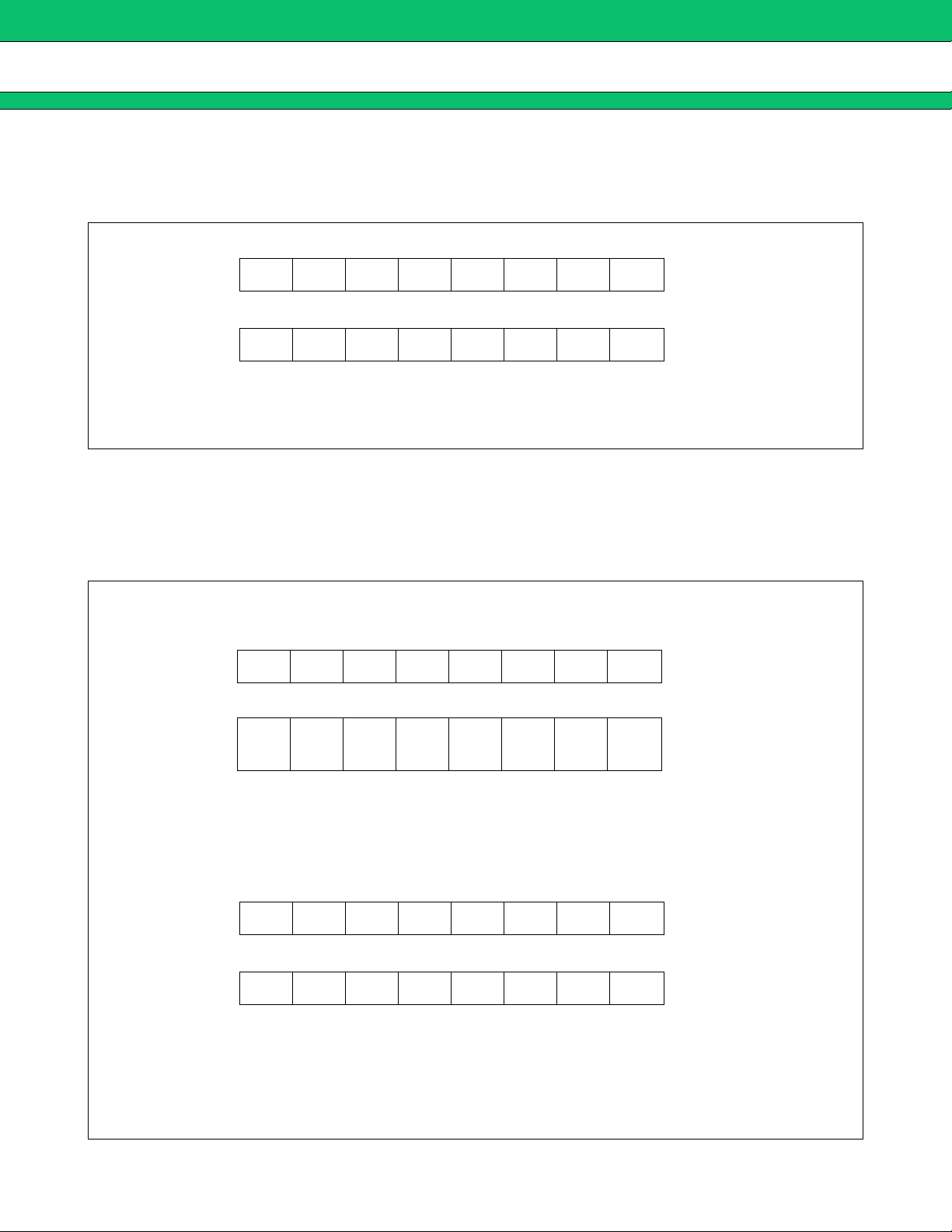
1. VRAM Address Setting (Command 0)
MSB LSB
MB90092
First byte
Second byte
1
MSB
0
RA6 RA5 CA4 CA3 CA2 CA1 CA0
VSL : VRAM write control
RA8 to RA5 : VRAM row address setting (0
CA4 to CA0 : VRAM column address setting (00
0000VSLRA8RA7
H to BH)
H to 17H)
2. VRAM Data Settings 1 and 2 (Commands 1 and 2)
(1) Writing main screen character control data (when command 0: VSL = 0)
• Command 1-1 (Main screen character control data setting 1)
MSB LSB
First byte
MSB
1
1000MAMBAT
LSB
LSB
Second byte
• Command 2-1 (Main screen character control data setting 2)
First byte
Second byte
0
CG CR CB MC
*: Parenthesized bit names are used for extended graphics mode.
MSB LSB
1
MSB
0
(MD), MC to M0 : Character code
AT : Specify character attribute display.
CG, CR, CB : Character colors
BG, BR, BB : Character background colors
(GR) : Specify normal character/graphic character display.
(BS) : Specify shaded background display.
M6 M5 M4 M3 M2 M1 M0
BG BR BB
(GR) (BS) (MD)
0010
*
M9 M8 M7
LSB
13

MB90092
(2) Writing sub-screen line control data (when command 0: VSL = 1, CA0 = 0)
• Command 1-2 (Sub-screen line control data setting 1)
MSB LSB
First byte
Second byte
• Command 2-2 (Sub-screen line control data setting 2)
First byte
Second byte
1
MSB
SCG SCR SCB SMC SGR SDC SMD
0
MSB LSB
1
MSB
SM6 SM5 SM4 SM3 SM2 SM1 SM0
0
SMD to SM0 : Sub-screen line first character code
SDC : Sub-screen line output control
SGR : Sub-screen line character display control
SCG to SCB : Sub-screen line character colors (when SGR = 0)
SCG : Sub-screen line graphic color transparency control (when SGR = 1)
SCR, SCB : Sub-screen line graphic color phase control (when SGR = 1)
SMA SMB 0
1000
SM9 SM8 SM7
0010
LSB
LSB
14

(3) Writing main screen control data (when command 0: VSL = 1, CA0 = 1)
• Command 1-3 (Main screen line control data setting 1)
MSB LSB
MB90092
First byte
Second byte
• Command 2-3 (Main screen line control data setting 2)
First byte
Second byte
1
MSB
0
MSB LSB
1
MSB
0
OF1, OF0 : Character color phase control
PC : Shaded pattern background color/monochrome control
PG, PR, PB : Shaded pattern background color
G2, G1, G0 : Character size control
SOC : Output priority control
VD : Video signal output control
DG : Digital signal output control
KC : Line background color/monochrome control
KG, KR, KB : Line background color
000PCPGPRPB
SOC VD DG KC KG KR KB
1000OF1OF0
0010G2G1G0
0
LSB
LSB
3. VRAM Write Control (Command 3)
MSB LSB
First byte
Second byte
1
MSB
0
FIL: VRAM fill control
0000000
1010FIL00
LSB
15

MB90092
4. Screen Control 1 (Command 4)
MSB LSB
First byte
Second byte
1
MSB
0
IE : Internal/external synchronization control
IN : Interlaced/noninterlaced display control
EB : Screen background display control
EO : Field control
CM : Color/monochrome display control
ZM : Zoom-in control
NP : NTSC/PAL control
P2, P0 : Pattern background control
DC : Display control
EO CM ZM NP P2 P0 DC
5. Screen Control 2 (Command 5)
MSB LSB
First byte
1
0001IEINEB
LSB
1001KIDAPCGYZ
Second byte
MSB
0
BH2 BH1 BH0 W3 W2 W1 W0
KID : Halftone control
APC : Reserve*
GYZ : Main screen line enlargement control
BH2 to BH0 : Reserve*
W3 to W0 : Main screen line spacing control
*: Reserve must be set at “ 0 ”.
LSB
16

6. Main Screen Line Control (Command 6)
MSB LSB
MB90092
First byte
Second byte
1
MSB
0
SOC VD DG N3 N2 N1 N0
G2 to G0 : Character size control
SOC : Output priority control
VD : Video signal output control
DG : Digital signal output control
N3 to N0 : Line specification
0011G2G1G0
7. Main Screen Vertical Display Position Control (Command 7)
MSB LSB
First byte
Second byte
MSB
1
0
0Y5Y4Y3Y2Y1Y0
1011ECLPFO
LSB
LSB
EC : Sync signal output control
LP : Simple NTSC/PAL control
FO : Color phase signal output control
Y5 to Y0 : Main screen vertical display position control
8. Main Screen Horizontal Display Position Control (Command 8)
MSB LSB
First byte
Second byte
1
MSB
0
SC : Sync signal input control
FC : Sync signal input 3 µs filter control
X5 to X0 : Main screen horizontal display position control
0X5X4X3X2X1X0
0100SC0FC
LSB
17

MB90092
9. Main Screen Display Mode Control (Command 9)
MSB LSB
First byte
Second byte
1
MSB
0
RP1
GRM: Main screen display mode control
RP1, RPO : Reserve 4*
S16 : Reserve 3*
SF1 : Reserve 2*
DW4 : Reserve 1*
RM1, RM0 : Reserve 0*
*: Reserve 0 to reserve 4 must be set at “0”.
10. Color Control (Command 10)
MSB LSB
First byte
1
MSB
RP0 S16
110000GRM
LSB
SF1
DW4
011000RB
RM1 RM0
LSB
Second byte
0
BK CC BC UC UG UR UB
RB : Main screen solid-fill background display control
BK : Main screen blink display control
CC : Main screen character color/monochrome control
BC : Main screen character background color/monochrome control
(Main screen graphic color/monochrome control)
UC : Screen background color/monochrome control
UG, UR, UB : Screen background color
18

11. Sub-Screen Control (Command 11)
MSB LSB
MB90092
First byte
Second byte
1
MSB
0
SG2 to SG0 : Sub-screen configuration control
SCC : Sub-screen character color/monochrome control
SBC : Sub-screen character background color/monochrome control
SGC : Sub-screen graphic color/monochrome control
SBG, SBR, SBB : Sub-screen pattern background color
0SCCSBC
1110 SG2 SG1 SG0
SGC
SBG SBR SBB
12. Sub-Screen Vertical Display Position Control (Command 12)
MSB LSB
First byte
Second byte
MSB
1
0
SY6 SY5 SY4 SY3 SY2 SY1 SY0
0101 SGA 0 SY7
LSB
LSB
SGA : Sub-screen full-screen mode control
SY7 to SY0 : Sub-screen vertical display position
13. Sub-Screen Horizontal Display Position Control (Command 13)
MSB LSB
First byte
Second byte
SX8 to SX0 : Sub-screen horizontal display position
MSB
1
0
SX6 SX5 SX4 SX3 SX2 SX1 SX0
1101 0 SX8 SX7
LSB
19

MB90092
ABSOLUTE MAXIMUM RATINGS
■■■■
Parameter Symbol
Unit Remarks
Min. Max.
VCC VSS – 0.3 VSS + 7.0 V *1
Rating
Supply voltage
AV
CC1VSS – 0.3 VSS + 7.0 V *1
AV
CC2VSS – 0.3 VSS + 7.0 V *1
Input voltage VIN VSS – 0.3 VSS + 7.0 V *2
Output voltage V
OUT VSS – 0.3 VSS + 7.0 V *2
Power consumption Pd — 600 mW
Operating temperature Ta –40 +85 °C
Storage temperature Tstg –55 +150 °C
*1: AVSS and VSS must have equal potential.
*2: Neither V
WARNING:
IN nor VOUT must exceed “VCC + 0.3 V.”
Semiconductor devices can be permanently damaged by application of stress (voltage, current,
temperature, etc.) in excess of absolute maximum ratings. Do not exceed these ratings.
RECOMMENDED OPERATING CONDITIONS
■■■■
(VSS = AVSS = 0 V)
Value
Parameter Symbol
Unit Remarks
Min. Max.
Specification guarantee
range
Supply voltage
V
CC 4.5 5.5 V
AV
CC1 4.5 5.5 V *1, *2
AV
CC2 4.5 5.5 V *1, *3
VIHS1 2.2 VCC + 0.3 V DA0 to DA7
“H” level input voltage
V
IHS2 0.8 × VCC VCC + 0.3 V Except DA0 to DA7
ILS1 –0.3 + 0.8 V DA0 to DA7
V
“L” level input voltage
VILS2 –0.3 0.2 × VCC V Except DA0 to DA7
Operating temperature Ta –40 +85 °C
Analog input voltage AV
*1: AV
SS and VSS must have equal potential.
*2: “AV
*3: “AV
WARNING:
CC1 = AVSS” is allowed if composite video signals (VIN-VOUT pins) are not used.
CC2 = AVSS” is allowed if Y/C-separated video signals (YIN-YOUT and CIN-COUT pins) are not used.
The recommended operating conditions are required in order to ensure the normal operation of the
IN 0VCC V
semiconductor device. All of the device’s electrical characteristics are warranted when the device is
operated within these ranges.
Always use semiconductor devices within their recommended operating condition ranges. Operation
outside these ranges may adversely affect reliability and could result in device failure.
No warranty is made with respect to uses, operating conditions, or combinations not represented on
the data sheet. Users considering application outside the listed conditions are advised to contact their
FUJITSU representatives beforehand.
20

ELECTRICAL CHARACTERISTICS
■■■■
1. DC Characteristics
Parameter
“H” level
output
voltage
“L” level
output
voltage
Input
current
Sym-
bol
V
OH
V
OL
I
IL
Pin Conditions
VOC, VOB, B,
R, G, HSYNC
VSYNC
VBLNK
READ
,
,
,
, FSCO,
ADR0 to ADR20
TESTI, CS,
SCLK, SIN,
EXHSYN
EXVSYN
,
,
CBCK,
DA0 to DA7,
TSC
, TEST
V
CC = 4.5 V
I
OH = –2 mA
VCC = 4.5 V
I
OL = 4.0 mA
VCC = 5.5 V
V
IL = 0.0 V
MB90092
(Ta = –40°C to +85°C, VSS = AVSS = 0 V)
Value
Min. Typ. Max.
4.0 — — V
——0.4V
–200 — –50 µA
Unit Remarks
Supply
current
Analog
supply
current
ON
resistance
Off
leakage
current
Output
resistance
VCC, AVCC1,
I
CC
AV
CC2
I
A AVCC1, AVCC2
VIN-VOUT,
YIN-YOUT,
R
ON
CIN-COUT,
VIN-VKOUT,
VKIN-VOUT
I
R
VIN, YIN, CIN,
OFF
VKIN
VOUT, YOUT,
OUT
COUT, VKOUT
CC = AVCC1 = AVCC2 = 5.5 V
V
4fsc = 17.734475 MHz
f
DC = 16.0 MHz
No load
CC = AVCC1 = AVCC2 = 5.5 V
V
4fsc = f
AV
DC = 0 MHz
IN = 1.65 V
No load
V
CC = AVCC1 = AVCC2 = 4.5 V
IOL = 100 µA
VCC = AVCC1 = AVCC2 = 5.5 V
AV
IN = 5.5 V
VCC = AVCC1 = AVCC2 = 4.5 V
IOL = 100 µA
——50mA
——30mA
—100320Ω
—0.110µA
100 — 1800 Ω
(Continued)
21

MB90092
Parameter
Yellow
High level
Sym-
bol
VYELH
Pin Conditions
(Ta = –40°C to +85°C, VSS = AVSS = 0 V)
Value
Min. Typ. Max.
Unit Remarks
2.89 3.00 3.11 V
Yellow
Low level
Cyan
High level
Cyan
Low level
Green
High level
Green
Low level
Magenta
High level
Magenta
Low level
Red
High level
Red
Low level
Blue
High level
V
YELL 2.03 2.14 2.25 V
VCYAH 2.89 3.00 3.11 V
V
CYAL 1.63 1.74 1.85 V
V
GREH 2.66 2.77 2.88 V
VGREL 1.63 1.74 1.85 V
V
MAGH 2.49 2.60 2.71 V
VOUT VCC = AVCC1 = AVCC2 = 5.0 V
V
MAGL 1.46 1.57 1.68 V
VREDH 2.49 2.60 2.71 V
V
REDL 1.23 1.34 1.45 V
V
BLUH 2.15 2.26 2.37 V
See Figure
“VOUT output”
Blue
Low level
Color burst
High level
Color burst
Low level
V
BLUL 1.23 1.34 1.45 V
VBSTH 1.80 1.91 2.02 V
V
BSTL 1.12 1.23 1.34 V
(Continued)
22

MB90092
Parameter
White level 3
φ = – 270°
White level 2
φ = – 180°
White level 1
φ = – 90°
White level 0
φ = 0°
Gray
level 6
Gray
level 5
Gray
level 4
Gray
level 3
Gray
level 2
Gray
level 1
Black
level 3
φ = – 270°
Sym-
bol
VWHT3
YWHT3
V
WHT2
YWHT2
VWHT1
YWHT1
V
WHT0
YWHT0
V
GRY6
YGRY6
VGRY5
YGRY5
V
GRY4
YGRY4
V
GRY3
YGRY3
VGRY2
YGRY2
V
GRY1
YGRY1
V
BLK3
YBLK3
Pin Conditions
VOUT,
YOUT
VCC = AVCC1 = AVCC2 = 5.0 V
(Ta = –40°C to +85°C, V
Values
Min. Typ. Max.
Unit Remarks
2.83 2.94 3.05 V
2.72 2.83 2.94 V
2.60 2.71 2.82 V
2.49 2.60 2.71 V
2.43 2.54 2.65 V
2.26 2.37 2.48 V
2.15 2.26 2.37 V
1.98 2.09 2.20 V
1.86 1.97 2.08 V
1.69 1.80 1.91 V
1.92 2.03 2.14 V
SS = AVSS = 0 V)
See
Figures
“VOUT
Output” and
“YOUT
Output”.
Black
level 2
φ = – 180°
Black
level 1
φ = – 90°
Black
level 0
φ = 0°
Pedestal
level
SYNC level
V
BLK2
YBLK2
V
BLK1
YBLK1
V
BLK0
YBLK0
V
PDS
YPDS
VTIP
YTIP
1.80 1.91 2.02 V
1.69 1.80 1.91 V
1.57 1.68 1.79 V
1.46 1.57 1.68 V
0.84 1.00 1.16 V
(Continued)
23

MB90092
(Continued)
Parameter
Sym-
bol
Pin Conditions
(Ta = –40°C to +85°C, VSS = AVSS = 0 V)
Value
Unit Remarks
Min. Typ. Max.
Yellow
High level
Yellow
Low level
Cyan
High level
Cyan
Low level
Green
High level
Green
Low level
Magenta
High level
Magenta
Low level
Red
High level
Red
Low level
YELH
C
YELL 1.00 1.11 1.22 V
C
C
CYAH 2.09 2.20 2.31 V
C
CYAL 0.89 1.00 1.11 V
1.92 2.03 2.14 V
CGREH 1.98 2.09 2.20 V
C
GREL 0.95 1.06 1.17 V
C
MAGH 1.98 2.09 2.20 V
CMAGL 0.95 1.06 1.17 V
C
REDH 2.09 2.20 2.31 V
C
REDL 0.89 1.00 1.11 V
COUT VCC = AVCC1 = AVCC2 = 5.0 V
See
Figure
“COUT
Output”
Blue
High level
Blue
Low level
Color burst
High level
Color burst
Low level
Pedestal
level
C
BLUH 1.92 2.03 2.14 V
CBLUL 1.00 1.11 1.22 V
C
BSTH 1.80 1.91 2.02 V
C
BSTL 1.12 1.23 1.34 V
CPDSC 1.46 1.57 1.68 V
24

• VOUT Output
MB90092
VWHT0 − 3
VGRY6
VGRY5
VGRY4
VBSTH
VPDS
VBSTL
VTIP
•
YOUT Output
YWHT0 − 3
YGRY6
YGRY5
YGRY4
YPDS
VYELH
VYELL
VCYAH
VCYAL
VGREH
VGREL
VMAGH
VMAGL
VREDH
VREDL
VBLUH
VBLUL
VGRY3
VGRY2
VGRY1
VBLK0 − 3
VPDS
YGRY3
YGRY2
YGRY1
YBLK0 − 3
YPDS
YTIP
•
COUT Output
CBSTH
CPDS
CBSTL
CYELH
CYELL
CCYAH
CCYAL
CGREH
CGREL
CMAGH
CMAGL
CREDH
CBLUH
CBLUL
CREDL
25

MB90092
2. AC Characteristics
(Ta = –40°C to +85°C, VCC = 5.0 V±10%, VSS = 0 V)
Parameter
Sym-
bol
Pin
Shift clock cycle time tCYC SCLK 1000 — ns
t
Shift clock pulse width
Shift clock signal rise/fall time
Shift clock start time t
Data setup time t
Data hold time t
Chip select end time t
Chip select signal rise/fall time
Horizontal sync signal rise time t
Horizontal sync signal fall time t
Vertical sync signal rise time t
Vertical sync signal fall time t
Horizontal sync signal pulse width*1 t
Vertical sync signal pulse width *1 t
Horizontal sync detection pulse width *2 t
Vertical sync detection pulse width*2 t
Reset input pulse width t
WCH
SCLK
t
WCL 450 — ns
t
CR
SCLK
t
CF — 200 ns
SS SCLK 200 — ns
SU SIN 200 — ns
H SIN 100 — ns
EC CS 500 — ns
t
CRC
CS
t
CFC — 200 ns
HR EXHSYN — 200 ns
HF EXHSYN — 200 ns
VR EXVSYN — 200 ns
VF EXVSYN — 200 ns
WH EXHSYN 4.0 8.0 µs
WV EXVSYN 15H
WCSH EXHSYN 4.0 8.0 µs
WCSV EXHSYN 13 28 µs
TESTI
WR
(TEST = Low)*3
Value
Min. Max.
450 — ns
— 200 ns
— 200 ns
10 — µs
Unit Remarks
See Figure “Serial Input
Timings”.
See Figure
“Vertical and Horizontal Sync
Signal Input Timings”.
See Figure “Composite Sync
Signal input Timings”.
See Figure “Reset Signal In-
put Timing”.
ROM read cycle *4 t
Address valid delay t
READ
active delay tra READ —38ns
Read data setup time t
Read data hold time t
Address invalid delay t
READ
inactive delay tri READ 0—ns
Tristate address delay t
Tristate READ
delay ttrd READ — 100 ns
rcyc — 250 500 ns
ab ADR0 to ADR20 — 60 ns
ds DA0 to DA7 30 — ns
dh DA0 to DA7 30 — ns
ai ADR0 to ADR20 0 — ns
tad ADR0 to ADR20 — 100 ns
*1: The values assume H/V-separated sync signal input.
*2: The values assume composite sync signal input.
*3: When the TEST
pin is a Low-lev el input, the TESTI pin serves as a reset pin input. (The TESTI and TEST pins
can be Low level at the same time.)
*4: Depends on the dot clock oscillation frequency. (t
26
rcyc = 4/fDC)
See Figure “Address Data
Hold Timings”.
See Figure “Address and
READ
Signal Delays at TSC
Signal Input”

•
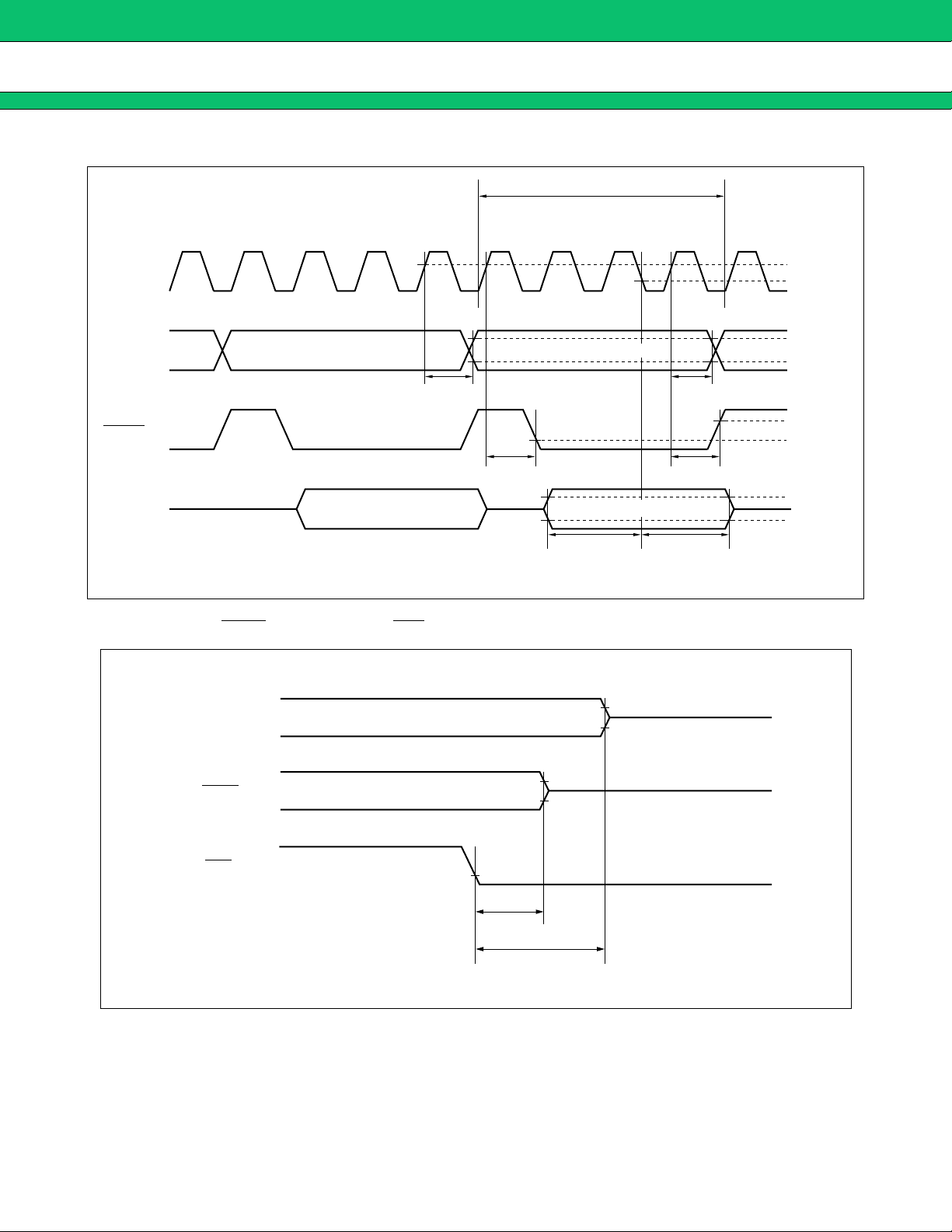
Serial Input Timings
MB90092
CS
0.8 VCC
tCFC
0.2 VCC
tSS
tCYC
SCLK
tCR tCF
tWCLtWCH
tSU
SIN
•
Vertical and Horizontal Sync Signal Input Timings
EXHSYN
0.8 VCC
0.2 VCC
0.8 VCC
0.2 VCC
tCRC
tEC
0.8 VCC
0.2 VCC
tH
0.8 VCC
0.2 VCC
0.8 VCC
0.2 VCC
EXVSYN
tHF
tVF
0.8 VCC
0.2 VCC
tWH
tWV
tHR
0.8 VCC
0.2 VCC
tVR
27

MB90092
•
Composite Sync Signal Input Timings
EXHSYN
EXHSYN
EXHSYN
tHF
0.8 V CC
0.2 V CC
tWCSH
0.8 V CC
0.2 V CC
tWCSV
H H
tWCSV
Vertical sync signal interval
(3H)
0.8 V CC
0.2 V CC
tHR
0.8 V CC
0.2 V CC
•
Reset Signal Input Timing
TESTI
0.2 VCC0.2 VCC
tWR
28
•
Address Data Hold Timings
4123412341
EXD
MB90092
trcyc
0.8 VCC
0.2 VCC
ADR0
to
ADR20
READ
DA0
to
DA7
•
Address and READ
ADR0 to ADR20
READ
Main screen data address *
tab
Main screen data *
*: The main screen and sub-screen have the same address data timings.
Signal Delays at TSC Signal Input
Sub-screen data address *
tra tri
Sub-screen data *
tds tdh
0.8 VCC
0.2 VCC
0.8 VCC
0.2 VCC
0.8 V
CC
0.2 VCC
tai
0.8 VCC
0.2 VCC
0.8 VCC
0.2 VCC
TSC
0.2 VCC
ttrd
ttad
29

MB90092
3. Clock Timing Specifications
Parameter Symbol Pin
Display dot clock* f
Color burst clock (NTSC)*
Min. Typ. Max.
DC EXD, XD 8 — 16 MHz
— 14.318185 — MHz
4 f
SC EXS, XS
Unit Remarks
Color burst clock (PAL)* — 17.734475 — MHz
* :Input the signal with a duty cycle of 50%.
4. Power -on Reset Specifications
(Ta = –40°C to +85°C)
Value
Parameter Symbol Pin
Power-supply rise time t
Power-supply off time t
Time after power-supply rise t
t
Reset cancel pulse width
tWRL 450 —
r
VCC
off 1—ms
WIT
WRH 450 —
CS
Value
Min. Max.
Unit Remarks
0.05 50 ms
450 — ns
ns
Conditions which activate
the power-on reset circuit
(See Figure “Power ON/
OFF Timing”).
Conditions in which the circuit repeatedly operate
normally (See Figure
“Power ON/OFF Timing”).
Power-on reset cancel timing (See Figure “Power-on
Reset Cancel Timing”).
30

•
Power ON/OFF Timing
MB90092
4.5 V
0.2 V 0.2 V
VCC
Note: The power supply must be activ a ted smoothly.
•
Power-on Reset Cancel Timing
VCC
Internal reset
CS
0.2 V
tr
toff
4.5 V
CS
tWIT
tWRL
tCRC* tCFC*
tWRH
*: See Section 2, “AC Characteristics”.
0.8 V CC
0.2 V CC
31

MB90092
5. Recommended Input Timings
(1) Composite sync signal input timing
Parameter NTSC PAL Unit Remarks
Number of frame scan lines 525 625 Lines
Field frequency 60 (59.94) 50 Hz *1
Line frequency 15750 (15734.264) 15625 Hz *1
Vertical retrace blanking interval 19 to 21 25 H *2
First equalizing pulse interval 3 2.5 H *2
Vertical sync pulse interval 3 2.5 H *2
Second equalizing pulse interval 3 2.5 H *2
Equalizing pulse width 2.29 to 2.54 2.34 to 2.36 µs
Equalizing pulse cycle 0.5 0.5 H *2
Cut-in pulse width 3.81 to 5.34 4.5 to 4.9 µs
Cut-in pulse cycle 0.5 0.5 H *2
Horizontal sync signal cycle 63.492 (63.5555) 64 µs
Horizontal sync signal pulse width 4.19 to 5.71 (4.7±0.1) 4.5 to 4.9 µs*1
Horizontal retrace blanking interval 10.2 to 11.4 (10.5 to 11.4) 11.7 to 12.3 µs*1
*1: Parenthesized values are specifications for color information display.
*2: 1 H is assumed to be one horizontal sync signal period.
(2) H/V-separated sync signal input timing
Parameter NTSC PAL Unit Remarks
Vertical sync signal frequency 60 (59.94) 50 Hz *1
Vertical sync signal pulse width 1 to 5 1 to 4 H *2
Horizontal sync signal cycle 63.492 (63.5555) 64 µs*1
Horizontal sync signal pulse width 4.19 to 5.71 (4.7±0.1) 4.5 to 4.9 µs*1
*1: Parenthesized values are specifications for color information display.
*2: 1 H is assumed to be one horizontal sync signal period.
32

6. Output Timings
(1) Horizontal timing
Symbol NTSC PAL Remarks
HPS 0 0
EQP1E 34 42
HPE 68 84
BSTS 76 100
BSTE 112 140
HBLKE 143 186
SEP1S 388 484
EQP2S 455 568
EQP2E 489 610
SEP2S 842 1050
HBLKS 888 1106
MB90092
See Figure “NTSC/PAL Horizontal Timings”.
IHCLR 910
*: Parenthesized values assume the last raster in each V cycle (field).
Note: The values in the above list are 4f
(2) Vertical timing
NTSC PAL
Symbol
Interlaced Noninterlaced Interlaced Noninterlaced
VPS0000
VPE6655
EQPE 12 12 10 10
VBLKE36364545
VBLKS 519 519 620 620
VPS 525 526 625 624
Note: The values in the above list are 1/2H count values.
SC count values.
1135
(1137)*
See Figures
“NTSC Vertical
Timings” and
“PAL Vertical
Timings”.
Remarks
33

MB90092
•
NTSC/PAL Horizontal Timings
Video signal
Horizontal sync signal
Horizontal retrace
blanking interval
Burst flag
Equalizing pulse
Cut-in pulse
HBLKE
BSTE
BSTS
HPE
EQP1E
HPS
HBLKS
EQP2E
EQP2S
SEP1S
IHCLR
HBLKS
SEP2S
34

•
NTSC Vertical Timings
MB90092
263
262261259258~2019~718654321525524523522521
260
1525524523522521~282~270 280268267265264262261259
281269263260 266
Composite video signal
Horizontal scanning line No.
Vertical sync interval
Even-numbered field
Vertical retrace blanking interval
VBLKS VPS VPE EQPE VBLKE VBLKS VPS
Equalizing pulse interval
Odd-numbered field
Composite video signal
VBLKS EQPE VBLKE VBLKS VPSVPS VPE
Horizontal scanning line No.
Vertical sync interval
Vertical retrace blanking interval
Equalizing pulse interval
35

MB90092
•
PAL Vertical Timings
Note 2
313
312311310309308~24~722654321625624622621
23
VPS
VBLKS
1625624622621~337336~320 335319317316315314312311310309
623
318
VPS
EQPE VBLKSBSTE VPE
313
312311310309308~24~722654321625624622621
23
VPS
1625624622621~337336~320 335319317316315314312311310309
623
318
VPS
EQPE VBLKSVPE
36
Note1
623
First field
Color burst phase
Composite video signal
Horizontal scanning line No.
Vertical sync interval
313
VBLKS VPS VPE BSTS VBLKE BSTE
BSTE EQPE
Second field
Color burst phase
Composite video signal
Horizontal scanning line No.
Vertical sync interval
Vertical retrace blanking interval
Burst blanking interval
Equalizing pulse interval
Vertical retrace blanking interval
623
VBLKS VPS BSTS VBLKE BSTE
Burst blanking interval
Third field
Equalizing pulse interval
Color burst phase
Composite video signal
Horizontal scanning line No.
313
VBLKS VPS VPE VBLKE
BSTE EQPE, BSTS BSTS, VBLKS
Color burst phase
Composite video signal
Vertical sync interval
Vertical retrace blanking interval
Burst blanking interval
Equalizing pulse interval
Horizontal scanning line No.
Forth field
BSTE, VBLKS VPS BSTS VBLKE BSTE
2: The arrows marks indicate the phase of color subcarrier. (↑: +135°, ↓: –135°)
Notes 1: indicates the HSYNC positions in the equalizing pulse intervals.
Vertical sync interval
Vertical retrace blanking interval
Burst blanking interval
Equalizing pulse interval

MB90092
SAMPLE CIRCUIT
■■■■
This is a standard example of the circuit to synthesize the character to input video signal or input internal
generation video signal from the outside. Note that composition is different according to the system and parts
used.
Composite
Y/C IN
IN
Video amplifer &
clamp circuit
Video amplifer &
clamp circuit
Sync separation
circuit
Control
microcontroller
+5 V
+
VIN
YIN
CIN
EXHSYN
CS
SCLK
SIN
CC1
AV
CC2
AV
MB90092
Composite OUT
VOUT
YOUT
COUT
D0
∼
D7
ADR0
∼
ADR20
READ OE CE
∼
∼
Buffer circuit
Buffer circuit
D0
∼
D7
A0
∼
A20
(16M − ROM)
Y/C OUT
+5 V
+
3.3 µH
20 pF 20 pF
(Approx. 14 MHz)
AV
VCC
VSS
XD
EXD
SS
EXS
XS
NTSC : 14.31818 MHz
PAL : 17.734475 MHz
37

MB90092
ORDERING INFORMATION
■■■■
Part number Package Remarks
MB90092PF
80-pin, plastic QFP
(QFP-80P-M06)
38

PACKAGE DIMENSION
■■■■
MB90092
80-pin plastic QFP
(FPT-80P-M06)
65
80
1 24
"A"
23.90±0.40(.941±.016)
20.00±0.20(.787±.008)
INDEX
0.80(.031)
0.37±0.05
(.015±.002)
Note : Pins width and pins thickness include plating thickness.
4164
40
0.10(.004)
17.90±0.40
(.705±.016)
14.00±0.20
(.551±.008)
Details of "A" part
0.20(.008)
25
3.05
.120 –.008
(Mounting height)
M
0.17±0.06
(.007±.002)
0.80±0.20
(.031±.008)
0.88±0.15
(.035±.006)
+0.30
–0.20
+.012
0.25(.010)
0~8°
0.30
.012
(Stand off)
+0.10
–0.25
+.004
–.010
C
2001 FUJITSU LIMITED F80010S-c-4-4
Dimensions in mm (inches).
39

MB90092
FUJITSU LIMITED
For further information please contact:
Japan
FUJITSU LIMITED
Marketing Division
Electronic Devices
Shinjuku Dai-Ichi Seimei Bldg. 7-1,
Nishishinjuku 2-chome, Shinjuku-ku,
Tokyo 163-0721, Japan
Tel: +81-3-5322-3353
Fax: +81-3-5322-3386
http://edevice.fujitsu.com/
North and South America
FUJITSU MICROELECTRONICS, INC.
3545 North First Street,
San Jose, CA 95134-1804, U.S.A.
Tel: +1-408-922-9000
Fax: +1-408-922-9179
Customer Response Center
Mon. - Fri.: 7 am - 5 pm (PST)
Tel: +1-800-866-8608
Fax: +1-408-922-9179
http://www.fujitsumicro.com/
Europe
FUJITSU MICROELECTRONICS EUR OPE GmbH
Am Siebenstein 6-10,
D-63303 Dreieich-Buchschlag,
Germany
Tel: +49-6103-690-0
Fax: +49-6103-690-122
http://www.fujitsu-fme.com/
Asia Pacific
FUJITSU MICROELECTRONICS ASIA PTE. LTD.
#05-08, 151 Lorong Chuan,
New Tech Park,
Singapore 556741
Tel: +65-281-0770
Fax: +65-281-0220
http://www.fmal.fujitsu.com/
Korea
FUJITSU MICROELECTRONICS K OREA LTD.
1702 KOSMO TOWER, 1002 Daechi-Dong,
Kangnam-Gu,Seoul 135-280
Korea
Tel: +82-2-3484-7100
Fax: +82-2-3484-7111
All Rights Reserved.
The contents of this document are subject to change without notice.
Customers are advised to consult with FUJITSU sales
representatives before ordering.
The information and circuit diagrams in this document are
presented as examples of semiconductor device applications, and
are not intended to be incorporated in devices for actual use. Also,
FUJITSU is unable to assume responsibility for infringement of
any patent rights or other rights of third parties arising from the use
of this information or circuit diagrams.
The products described in this document are designed, and
manufactured as contemplated for general use, including without
limitation, ordinary industrial use, general office use, personal use,
and household use, but are not designed, developed and
manufactured as contemplated (1) for use accompanying fatal risks
or dangers that, unless extremely high safety is secured, could have
a serious effect to the public, and could lead directly to death,
personal injury, severe physical damage or other loss (i.e., nuclear
reaction control in nuclear facility, aircraft flight control, air traffic
control, mass transport control, medical life support system, missile
launch control in weapon system), or (2) for use requiring
extremely high reliability (i.e., submersible repeater and artificial
satellite).
Please note that Fujitsu will not be liable against you and/or any
third party for any claims or damages arising in connection with
above-mentioned uses of the products.
Any semiconductor devices have inherently a certain rate of failure.
You must protect against injury, damage or loss from such failures
by incorporating safety design measures into your facility and
equipment such as redundancy, fire protection, and prevention of
over-current levels and other abnormal operating conditions.
If any products described in this document represent goods or
technologies subject to certain restrictions on export under the
Foreign Exchange and Foreign Trade Control Law of Japan, the
prior authorization by Japanese government should be required for
export of those products from Japan.
40
F0108
FUJITSU LIMITED Printed in Japan
 Loading...