


查询MB90050供应商
FUJITSU SEMICONDUCTOR
DATA SHEET
ASSP For Screen Display Control
CMOS
On-Screen Display Controller
MB90050
DESCRIPTION
■
The MB90050 is an on-screen display controller for displaying text and graphics on the TV screen.
The MB90050 controls a display area of 35 characters b y 16 lines, and provides each char acter composed of 24
× 32 dots at most. The display functions include a wealth of characters with qualifying functions such as char acter
background shading (shadow casting) , sprite character functions and graphic character functions, contr ibuting
to the use of control GUI displays. The MB90050 incorporates display memory (VRAM) , character font ROM,
and sync signal generation circuit and video signal generation circuit supporting the NTSC and PAL systems,
allowing text and graphics to be displayed in conjunction with a small number of external components.
DS04-28829-2E
FEATURES
■
• Main screen display capacity
35 characters × 16 lines (maximum 560 characters)
• Character configuration
Normal characters : 24 × 32 dots
Graphic characters : 12 × 16 dots* (colorable per 1 dot)
PACKAGE
■
48-pin plastic QFP
(FPT-48P-M15)
(Continued)

MB90050
• Font display configuration
Three horizontal width settings (selectable setting L/M/S for each character) per character.
L size : 24 dots
M size : 18 dots
S size : 12 dots
Two vertical height settings (selectable A/B for each line) per line.
A : 18 to 32 dots (setting per 2 dots)
B : 18 to 32 dots (setting per 2 dots)
(These sizes are dot sizes of typical character. Each size of graphic characters uses half the number of dots
of typical characters. Note, ho we ver, that both of the typical and graphic characters are the same in character
area size.)
• Character types
Usable all 512 character types (font ROM+, font RAM)
Font ROM : 512 character types (all area user setting)
Font RAM : 8 character types (all area user command setting)
Capable of setting a specific eight-character area in font ROM so that the area is replaced with font RAM.
•Display modes
Character : Normal character/graphic character (set for each character)
Character trimming : Side trimming 1/side trimming 2/patern background 1/patern background 2
(set for each screen)
Character background : None/Solid-fill/Shaded background (concave) /Shaded background (convex)
(set for each character)
Line background : None/Solid-fill/Shaded background (concave) /Shaded background (convex)
(set for each line)
Character enlargement : Normal, Double width, Double height, Double width × doub le height (set for each line)
Brink : OFF/ON (set for each character)
• Main screen display position control
Horizontal display position : Control in 2-dot units (movable through the entire screen)
Vertical display position : Control in 2-dot units (movable through the entire screen)
Line spacing control : 0 to 14 dots, 2-dot units (set for each line)
Sprite character display control
Capable of displaying one block for an arbitrary character on the topmost layer on the screen.
Sprite character display : OFF/ON (graphic character display)
Sprite character types : 256 types (character codes 000
Sprite character configuration : 1 character/2 characters horizontal/2 characters vertical/
2×2 characters
Sprite character horizontal display position : Control in 1-dot units
Sprite character vertical display position : Control in 1-dot units
Screen background color display control
Capable of displaying an arbitrary color on the entire bottommost layer on the screen.
Screen background color display : OFF/ON
• Display colors
Digital output : 16 colors selectable from among 64 colors (built in palette circuit)
Video output : Any 16 colors selectable (Command setting enable)
to 0FFH)
H
(Continued)
2

(Continued)
• Display colors and setting units
Character color : 16 colors (set for each character)
Character background color : 16 colors (set for each character)
Character trimming color : 16 colors (set for each line)
Line background color : 16 colors (set for each line)
Graphic character color : 16 colors (set for each dot)
Sprite character color : 16 colors (set for each dot)
Screen background character color : 16 colors (set for each dot)
Screen background color : 16 colors (set for all screen)
Shaded background frame highlight color : 16 colors (set for all screen)
Shaded background frame shadow color : 16 colors (set for all screen)
• Digital display signal output
Color signal output : DCOL5 to DCOL0 pins (6 bits)
Display period signal output : DB pin
Translucent display period signal output : DH pin
• Analog (video) signal input/output
Composit video input/output : VIN, VOUT pins
Y/C video input/output : YIN, YOUT pins, CIN, COUT pins
• Internal sync control
Internal sync signal generator and video signal generator supporting the NTSC and PAL systems.
• External interface
16-bit serial input (3-signal input)
Chip select signal
Serial clock signal
Serial data signal
• Package
QFP-48P (FPT-48P-M15)
• Supply voltage
+5 V±10%
MB90050
* : 1 dot of graphic characters is the same size as 2 × 2 dots of normal characters.
3

MB90050
PIN ASSIGNMENT
■
(TOP VIEW)
FLDI
VSYNCI
HSYNCI
V
CC
VSS
EXS
XS
FSC4O
VSYNCO
HSYNCO
CSYNCO
VBLKO
1
2
3
4
5
6
7
8
9
10
11
12
YOUT
48
TESTI2
47
YIN
46
SS2
AV
45
CC2
CIN
AV
44
43
MB90050
COUT
42
SS1
AV
41
VOUT
40
CC1
AV
39
VIN
38
TESTI1
37
36
35
34
33
32
31
30
29
28
27
26
25
PO3
PO2
DCOL5
DCOL4
DCOL3
DCOL2
DCOL1
DCOL0
DCLKO
DB
DH
RESET
13
14
15
16
17
18
19
20
21
22
23
24
FLDO
CS
SYNCST
SCLK
SIN
XD
BUSY
EXD
SS
V
VCC
PO0
PO1
(FPT-48P-M15)
4

PIN DESCRIPTIONS
■
MB90050
Pin
Pin name I/O
no.
6,
7
20,
19
15 CS
16 SCLK I C
17 SIN I C
18 BUSY O F
2 VSYNCI
3 HSYNCI
1FLDIID
EXS,
XS
EXD,
XD
Circuit
type
I/O A
I/O B
IC
ID
ID
Function
Crystal oscillation circuit pins for color burst clock generator.
Connect an external crystal oscillator (14.31818 MHz for NTSC or 17.734475
MHz for PAL) and load capacitance (C) to these pins to form a crystal oscillation
circuit.
LC oscillation circuit pins for display dot clock generator.
Connect these pins to external “L” and “C” to from an LC oscillation circuit.
Chip select signal input pin.
For serial command transfer, set this pin to the Low level.
Serial clock signal input pin.
This pin feeds a clock signal upon transfer of a serial command. It feeds serial
data at the rising edge.
Serial data signal input pin.
Input data during serial command transfer.
Busy signal output pin.
This pin outputs a significant level signal during VRAM filling. Do not input a
serial command while the pin outputs the significant level signal.
Supplying a low level signal to the CS
put period terminates the VRAM fill operation and causes this pin to output an
insignificant level signal.
The pin enables output (ON/OFF) control, output logic control, and internal pullup ON/OFF control depending on the command setting.
When the RESET
turns off the internal pull-up resistor, and sets the output to OFF (output tied to
the low).
Vertical sync signal input pin.
Active low signal or active high signal input is command-selectable for the pin.
When the RESET pin inputs the low level signal, this pin inputs the active low
signal.
Horizontal sync signal input pin.
Active low signal or active high signal input is command-selectable for the pin.
When the RESET pin inputs the low level signal, this pin inputs the active low,
horizontal sync signal.
Field signal input pin.
The internal field signal identically detected from among input sync signals or the
input signal to this pin is command-selectable for field control.
During operation under external synchronization control, the input signal is used
to control the least significant bit of the font ROM/RAM raster address.
The input signal to this pin is disabled during operation under internal synchronization control.
pin inputs a low level signal, this pin outputs the busy signal,
pin during the significant level signal out-
(Continued)
5

MB90050
Pin
no.
9VSYNCO
10 HSYNCO
11 CSYNCO
12 VBLKO O F
13 FLDO O F
14 SYNCST O F
Pin
name
Circuit
I/O
type
OF
OF
OF
Function
Vertical sync signal output pin.
The pin enables output (ON/OFF) control, output logic control, and internal pullup ON/OFF control depending on the command setting.
When the RESET
pull-up resistor and sets the output to OFF (output tied to the high).
Horizontal sync signal output pin.
The pin enables output (ON/OFF) control, output logic control, and internal pullup ON/OFF control depending on the command setting.
When the RESET
pull-up resistor and sets the output to OFF (output tied to the high).
Composite sync signal output pin.
The pin enables output (ON/OFF) control, output logic control, and internal pullup ON/OFF control depending on the command setting.
When the RESET
pull-up resistor and sets the output to OFF (output tied to the high).
Vertical blanking interval (VBI) output pin.
The pin enables output (ON/OFF) control, output logic control, and internal pullup ON/OFF control depending on the command setting.
When the RESET
pull-up resistor and sets the output to OFF (output tied to the low).
Field signal output pin.
During operation under internal synchronization control, this pin outputs the internally generated field signal.
During operation under external synchronization control, the pin outputs the
field signal (internally detected field signal or external input field signal) used for
internal operations.
The pin enables output (ON/OFF) control, output logic control, and internal pullup ON/OFF control depending on the command setting.
When the RESET
pull-up resistor and sets the output to OFF (output tied to the low).
Synchronization detection signal output pin.
This pin outputs a significant level signal with a sync signal detected and an insignificant level signal with no sync signal detected.
The pin enables output (ON/OFF) control, output logic control, and internal pullup ON/OFF control depending on the command setting.
When the RESET
pull-up resistor and sets the output to OFF (output tied to the low).
pin inputs the low level signal, this pin turns off the internal
pin inputs the low level signal, this pin turns off the internal
pin inputs the low level signal, this pin turns off the internal
pin inputs the low level signal, this pin turns off the internal
pin inputs the low level signal, this pin turns off the internal
pin inputs the low level signal, this pin turns off the internal
(Continued)
6

MB90050
Pin
no.
28 DCLKO O G
8FSC4OO G
26 DH O (I) H
27 DB O (I) H
34,
33,
32,
31,
30,
29
36,
35,
24,
23
Pin
name
DCOL5,
DCOL4,
DCOL3,
DCOL2,
DCOL1,
DCOL0
PO3,
PO2,
PO1,
PO0
Circuit
I/O
type
O (I) H
O (I) H
Function
Dot clock signal output pin.
This pin outputs an LC oscillation clock signal.
The pin enables output (ON/OFF) control depending on the command setting.
The normal clock (that stops oscillation during horizontal synchronization) or continuous clock (that does not stop oscillation during horizontal synchronization*)
can be command-selected for the output using the command setting for output selection control (CKS).
When the TESTI2
clock signal that does not stop oscillation during horizontal synchronization
(where the output selection control (CKS) setting is disabled).
When the RESET
* : For continuous clock, this pin is used for frequency measurement. To measure
the dot clock, the pin sets display signal output that is not the standard and
cannot display correctly.
Crystal oscillator 4FSC clock signal output pin.
This pin enables output (ON/OFF) control depending on the command setting.
The crystal oscillation clock (4FSC) or its 1/4 frequency clock (FSC) can be command-selected for the output using the command setting for output selection control (FSS).
When the TESTI2
signal (where the output selection control (FSS) setting is disabled).
When the RESET
signal.
Halftone display period signal output pin.
This pin enables output (ON/OFF) control and output logic control depending on
the command setting.
When the RESET
(output tied to the low).
(The input feature of the pin is a test function. Use the pin usually only for output.)
Display period signal output pin.
This pin enables output (ON/OFF) control and output logic control depending on
the command setting. When the RESET
sets the output to OFF (entering the low level signal fixed output state).
(The input feature of the pin is a test function. Use the pin usually only for output.)
Display color signal output pin.
This pin enables output (ON/OFF) control and output logic control depending on
the command setting. When the RESET
sets the output to OFF (entering the low level signal fixed output state).
(The input feature of the pin is a test function. Use the pin usually only for output.)
Port signal output pin.
This pin enables output level (High/Low) control depending on the command setting. When the RESET
OFF (entering the low level signal fixed output state).
(The input feature of the pin is a test function. Use the pin usually only for output.)
pin inputs a low level signal, this pin outputs the continuous
pin inputs the low level signal, the pin outputs a dot clock signal.
pin inputs the low level signal, this pin outputs the 4FSC clock
pin inputs the low level signal, this pin outputs the 4FSC clock
pin inputs the low level signal, this pin sets the output to OFF
pin inputs the low level signal, this pin
pin inputs the low level signal, this pin
pin inputs the low level signal, this pin sets the output to
(Continued)
7

MB90050
(Continued)
Pin
no.
25 RESET
37 TESTI1
47 TESTI2
Pin
name
I/O
Circuit
IC
IE
I E Test signal input pin. Input High level signal during normal operation.
38 VIN I I
46 YIN I I
44 CIN I I
40 VOUT O I
type
Function
Reset signal input pin.
Upon input of the low level signal, this pin causes an internal reset.
After the power supply is inserted, the reset input is required for normal operation.
During regular operation, the pin inputs the high level signal.
Test signal input pin. Input High level signal during normal operation.
(Input of the Low level signal activates test mode operation.)
Composite video signal input pin. This pin inputs a DC-reproduced signal of
2 V
(pedestal level 1.57 V, sync tip level 1 V) .
P-P
Luminance video signal (Y video signal) input pin.
This pin inputs a DC-reproduced signal of 2 V
(pedestal level 1.57 V, sync
P-P
tip level 1 V) .
Saturation video signal (C video signal) input pin.
This pin inputs a signal at 1.57 VDC and a color burst signal amplitude of 0.57
V
.
P-P
Composite video signal output pin.
This pin outputs a signal of 2 V
When the RESET
signal inputs the low level signal, this pin outputs the black
(pedestal level 1.57 V, sync tip level 1 V) .
P-P
video (pedestal level without color burst) signal.
48 YOUT O I
42 COUT O I
4,
22
5,
21
39 AV
43 AV
41,45AV
V
V
AV
CC
SS
CC1
CC2
SS1
SS2
⎯⎯
⎯⎯
⎯⎯
⎯⎯
,
⎯⎯
Luminance video signal (Y video signal) output pin.
This pin outputs a signal of 2 V
When the RESET
pin inputs the low level signal, this pin outputs the black
(pedestal level 1.57 V, sync tip level 1 V) .
P-P
video (pedestal level) signal.
Saturation video signal (C video signal) output pin.
This pin outputs a signal at 1.57 VDC and a color burst signal amplitude of
0.57 V
When the RESET
P-P
.
pin inputs the low level signal, this pin outputs the black
video signal (a DC voltage of 1.57 V without color burst).
Power supply pin for digital circuit. These pins supply
5 V and make all VCC
+
pins same potential.
Digital ground pins. These pins make all V
pins and AV
SS
SS1
/AV
pins same
SS2
potential.
Power supply pin for analog circuit and composite video signal Input/Output
(VIN-VOUT) circuit. This pin supplies +5 V. Input analog ground level when
not using this analog circuit.
Power supply pin for analog circuit, luminance video signal Input/Output
(YIN-YOUT) circuit, and saturation video signal Input/Output (CIN-COUT)
circuit. This pin supplies +5 V. Input analog ground level when not using this
analog circuit.
Analog ground pins. AV
V
pins make these pins same potential.
SS
pin makes AV
SS1
pin same potential.
SS2
8

I/O CIRCUIT TYPES
■
Type Circuit Remarks
• Crystal oscillation
Oscillator feedback resistor
EXS
(approx. 1MΩ)
MB90050
A
XS
TEST signal
• LC oscillation
EXD
B
XD
STOP signal
• TTL level, Hysteresis input
C
TTL
• CMOS level, Hysteresis input
D
CMOS
• CMOS level, Hysteresis input
5 V
with pull-up resistor (approx. 50 kΩ)
E
CMOS
(Continued)
9

MB90050
l
(Continued)
Type Circuit Remarks
• Nch open-drain output
5 V
Pch
F
Nch
5 V
Pch
Pull-up
control signal
G
Nch
with pull-up resistor SW
(approx. 50 kΩ)
• CMOS output
•CMOS I/O
5 V
Pch
Input is for test.
H
Nch
TEST signal
Input
(TEST)
• Analog I/O
CMOS analog SW
I
Control signa
10

■ BLOCK DIAGRAM
SIN
SCLK
CS
Serial input
control
MB90050
Each block
VIN
YIN
CIN
HSYNCI
VSYNCI
FLDI
SYNCST
HSYNCO
VSYNCO
CSYNCO
FLDO
VBLKO
BUSY
Sync control
NTSC/PAL
signal
generator
circuit
Video signal
generator circuit
Palette
(4 bits→6 bits)
Display Memory control
Analog
switch
Output control
VOUT
YOUT
COUT
DCOL5 to DCOL0
DB
DH
EXS
XS
FSC4O
EXD
XD
DCLKO
RESET
VRAM
(35 characters
× 16 lines)
4FSC clock
oscillation
circuit
Dot clock
oscillation
circuit
Font ROM
(512 characters)
Each block
Each block
All reset
Font RAM
(8 characters)
Port control
PO3
PO2
PO1
PO0
11

MB90050
ABSOLUTE MAXIMUM RATINGS
■
Parameter Symbol
Unit Remarks
Min Max
Rating
V
Power supply voltage*
1
AV
AV
Input voltage*
Output voltage*
1
1
V
V
“L” level maximum output current I
“H” level maximum output current I
Power consumption P
CC
CC1
CC2
IN
OUT
OL
OH
d
VSS − 0.5 VSS + 7.0 V *2
VSS − 0.5 VSS + 7.0 V *2
VSS − 0.5 VSS + 7.0 V *2
VSS − 0.5 VCC + 0.5 V
VSS − 0.5 VCC + 0.5 V
⎯ 15 mA
⎯−15 mA
⎯ 500 mW
Operating temperature Ta −40 +85 °C
Storage temperature Tstg −55 +125 °C
*1 : The parameter is based on VSS = AV
*2 : Do not make a potential difference between AV
SS1
= AV
SS2
= 0 V.
(AV
SS
SS1
/AV
) pins and VSS pin.
SS2
WARNING: Semiconductor devices can be permanently damaged by application of stress (voltage, current,
temperature, etc.) in excess of absolute maximum ratings. Do not exceed these ratings.
12

RECOMMENDED OPERATING CONDITIONS
■
MB90050
(VSS = AV
SS1
= AV
SS2
= 0 V)
Parameter Symbol
Unit
Min Max
Value
Power supply voltage
“H” level input voltage
“L” level input voltage
AV
AV
V
V
V
V
A
V
V
V
CC
CC1
CC2
IH1
IH1S
IH2S
IL1
IL1S
IL2S
VIN1
4.5 5.5 V
4.5 5.5 V *1, *2
4.5 5.5 V *1, *3
0.7 × V
0.8 × V
0.6 × V
CC
CC
CC
VSS − 0.3 0.3 × V
VSS − 0.3 0.2 × V
VCC + 0.3 V (H)
VCC + 0.3 V (D, E)
VCC + 0.3 V (C)
CC
CC
VSS − 0.3 0.6 V (C)
0AV
CC1
Analog input voltage
A
VIN2
0AV
CC2
Operating temperature Ta −40 +85 °C
*1 : Do not make a potential difference between AV
*2 : It is possible to set AV
*3 : It is possible to set A V
= AVSS (AV
CC1
= AVSS (A V
CC2
SS1
SS1
/AV
/AV
SS2
(AV
/AV
SS
SS1
) when not using composite video signal (VIN pin, VOUT pin) .
SS2
) pins and VSS pin.
SS2
) when not using Y/C separated video signals (YIN pin, Y OUT pin,
CIN pin and COUT pin) .
Remarks
(circuit type)
V(H)
V(D, E)
V VIN pin
V YIN pin, CIN pin
WARNING: The recommended operating conditions are required in order to ensure the normal operation of the
semiconductor device. All of the device’s electrical characteristics are warranted when the device is
operated within these ranges.
Always use semiconductor devices within their recommended operating condition ranges. Operation
outside these ranges may adversely affect reliability and could result in device failure.
No warranty is made with respect to uses, operating conditions, or combinations not represented on
the data sheet. Users considering application outside the listed conditions are advised to contact their
FUJITSU representatives beforehand.
13

MB90050
ELECTRICAL CHARACTERISTICS
■
1. DC Characteristics
(VSS = AV
SS1
= AV
= 0 V, Ta = −40 °C to +85 °C)
SS2
Parameter
Sym-
bol
“H” level output voltage V
“L” level output voltage V
Pull-up resistor R
Power supply current I
Analog power supply
current
ON resistor R
OFF leak current I
Output resistor R
OH
OL
CC
I
A
ON
OFF
OUT
P
Pin name Conditions
Value
Min Typ Max
All output
pins
All output
pins
VCC = 4.5 V,
I
= −4.0 mA
OH
VCC = 4.5 V,
I
= 4.0 mA
OL
4.0 ⎯⎯V
⎯⎯0.4 V
E, F VCC = 5.5 V 25 50 200 kΩ
VCC = 5.5 V,
4FSC = 20 MHz,
f
= 20 MHz
DC
VCC = AV
4FSC = 0 MHz,
,
AV
= AV
IN1
= AV
CC1
= 1.65 V,
IN2
= 5.5 V,
CC2
⎯ 35 45 mA
⎯ 22 40 mA
AV
AV
V
CC
CC1
CC2
No load
VIN-VOUT,
YIN-YOUT,
CIN-COUT
VIN,
YIN,
CIN
VOUT,
YOUT,
COUT
V
= AV
CC
I
= 100 µA
OL
V
= AV
CC
AV
= AV
IN1
V
= AV
CC
I
= 100 µA
OL
CC1
CC1
IN2
CC1
= AV
= AV
= 5.5 V
= AV
= 4.5 V,
CC2
= 5.5 V,
CC2
= 4.5 V,
CC2
⎯ 215 310 Ω
⎯ 0.1 10 µA
100 ⎯ 1800 Ω
Unit
14

MB90050
Analog Ladder Voltage
(V
= AV
CC
Symbol Parameter
Min Typ Max
Value
VOHR0 Resistance ladder voltage 00 (−40 IRE) 930 1000 1040 mV
VOHR1 Resistance ladder voltage 01 (−36 IRE) 988 1057 1098 mV
VOHR2 Resistance ladder voltage 02 (−32 IRE) 1046 1114 1156 mV
VOHR3 Resistance ladder voltage 03 (−28 IRE) 1104 1171 1214 mV
VOHR4 Resistance ladder voltage 04 (−24 IRE) 1162 1229 1272 mV
VOHR5 Resistance ladder voltage 05 (−20 IRE) 1220 1286 1330 mV
VOHR6 Resistance ladder voltage 06 (−16 IRE) 1278 1343 1388 mV
VOHR7 Resistance ladder voltage 07 (−12 IRE) 1336 1400 1446 mV
VOHR8 Resistance ladder voltage 08 (−8 IRE) 1394 1457 1504 mV
VOHR9 Resistance ladder voltage 09 (−4 IRE) 1452 1514 1562 mV
VOHR10 Resistance ladder voltage 10 (0 IRE) 1510 1571 1620 mV
VOHR11 Resistance ladder voltage 11 (4 IRE) 1568 1629 1678 mV
VOHR12 Resistance ladder voltage 12 (8 IRE) 1626 1686 1736 mV
VOHR13 Resistance ladder voltage 13 (12 IRE) 1684 1743 1794 mV
VOHR14 Resistance ladder voltage 14 (16 IRE) 1742 1800 1852 mV
VOHR15 Resistance ladder voltage 15 (20 IRE) 1800 1857 1910 mV
VOHR16 Resistance ladder voltage 16 (24 IRE) 1858 1914 1968 mV
VOHR17 Resistance ladder voltage 17 (28 IRE) 1916 1971 2026 mV
VOHR18 Resistance ladder voltage 18 (32 IRE) 1974 2029 2084 mV
VOHR19 Resistance ladder voltage 19 (36 IRE) 2032 2086 2142 mV
VOHR20 Resistance ladder voltage 20 (40 IRE) 2090 2143 2200 mV
VOHR21 Resistance ladder voltage 21 (44 IRE) 2148 2200 2258 mV
VOHR22 Resistance ladder voltage 22 (48 IRE) 2206 2257 2316 mV
VOHR23 Resistance ladder voltage 23 (52 IRE) 2264 2314 2374 mV
VOHR24 Resistance ladder voltage 24 (56 IRE) 2322 2371 2432 mV
VOHR25 Resistance ladder voltage 25 (60 IRE) 2380 2429 2490 mV
VOHR26 Resistance ladder voltage 26 (64 IRE) 2438 2486 2548 mV
VOHR27 Resistance ladder voltage 27 (68 IRE) 2496 2543 2606 mV
VOHR28 Resistance ladder voltage 28 (72 IRE) 2554 2600 2664 mV
VOHR29 Resistance ladder voltage 29 (76 IRE) 2612 2657 2722 mV
VOHR30 Resistance ladder voltage 30 (80 IRE) 2670 2714 2780 mV
VOHR31 Resistance ladder voltage 31 (84 IRE) 2728 2771 2838 mV
VOHR32 Resistance ladder voltage 32 (88 IRE) 2786 2829 2896 mV
VOHR33 Resistance ladder voltage 33 (92 IRE) 2844 2886 2954 mV
VOHR34 Resistance ladder voltage 34 (96 IRE) 2902 2943 3012 mV
VOHR35 Resistance ladder voltage 35 (100 IRE) 2960 3000 3070 mV
CC1
= AV
= 5.0 V)
CC2
Unit
15

MB90050
MB90050 Palette Initial Value
• Pedestal level
Color code Comment
⎯ Pedestal 0 40 0A
• Sink chip level
Color code Comment
⎯ Sink chip −40 0 00
• Translucence level
Color code Comment
⎯ translucence 32 72 12
Relative value Absolute value Register setting value
PED (IRE) PED (IRE) PED (HEX)
Relative value Absolute value Register setting value
SYN (IRE) SYN (IRE) SYN (HEX)
Relative value Absolute value Register setting value
HAN (IRE) HAN (IRE) HAN (HEX)
• Color burst level
Relative value Absolute value Register setting value
Color code Comment
BST0
(IRE)
BST1
(IRE)
BST2
(IRE)
BST3
(IRE)
BST0
(IRE)
BST1
(IRE)
BST2
(IRE)
BST3
(IRE)
BST0
(HEX)
BST1
(HEX)
BST2
(HEX)
⎯ Burst 0 −240 24401640640A040A10
• Y (COLOR)
Relative value Absolute value Register setting value
Color code Comment
Luminance (IRE) YD (IRE) YD (HEX)
15 White-1 100 140 23
14 Yellow-1 72 112 1C
13 Cyan-1 64 104 1A
12 Green-1 56 96 18
11 Magenta-1 40 80 14
10 Red-1 32 72 12
9 Blue-1 24 64 10
8 Black-1 16 56 0E
7 White-0 92 132 21
6 Yellow-0 64 104 1A
5Cyan-0 56 96 18
BST3
(HEX)
16
4 Green-0 48 88 16
3 Magenta-0 32 72 12
2 Red-0 24 64 10
1 Blue-0 16 56 0E
0Black-0 8 48 0C

MB90050
• C (COLOR)
Relative value Absolute value Register setting value
Color code Comment
15 White-1 0 0 40404040 0A 0A 0A 0A
14 Yellow-1 195 20 35 21 45 59 09 05 0B 0F
13 Cyan-1 284 36 5 49 75 31 01 0C 13 08
12 Green-1 241 30 14 25 66 55 03 06 11 0E
11 Magenta-1 61 30 66 55 14 25 11 0E 03 06
10 Red-1 104 36 75 31 5 49 13 08 01 0C
9 Blue-1 15 20 455935210B 0F 09 05
8 Black-1 0 0 40 40 40 40 0A 0A 0A 0A
7 White-0 0 0 40 40 40 40 0A 0A 0A 0A
6 Yellow-0 195 20 35 21 45 59 09 05 0B 0F
5 Cyan-0 284 36 5 49 75 31 01 0C 13 08
4 Green-0 241 30 14 25 66 55 03 06 11 0E
3 Magenta-0 61 30 66 55 14 25 11 0E 03 06
2 Red-0 104 36 75315491308010C
1 Blue-0 15 20 455935210B 0F 09 05
0 Black-0 0 0 40 40 40 40 0A 0A 0A 0A
Phase
(degrees)
Amplitude
(IRE)
0 90 180 270
CD0
(HEX)
CD1
(HEX)
CD2
(HEX)
CD3
(HEX)
• V (COLOR)
Absolute value Register setting value
Color code Comment
0 90 180 270
15 White-1 140 140 140 140 23 23 23 23
14 Yellow-1 107 93 117 131 1B 17 1D 21
13 Cyan-1 69 113 139 95 11 1C 23 18
12 Green-1 70 81 122 111 11 14 1F 1C
11 Magenta-1 106 95 54 65 1B 18 0D 10
10 Red-1 107 63 37 81 1B 10 09 14
9 Blue-1 6983594511150F0B
8 Black-1 56 56 56 56 0E 0E 0E 0E
7 White-0 132 132 132 132 21 21 21 21
6 Yellow-0 99 85 109 123 19 15 1B 1F
5 Cyan-0 61 105 131 87 0F 1A 21 16
4 Green-0 62 73 114 103 0F 12 1D 1A
3 Magenta-0 98 87 46 57 19 16 0B 0E
2 Red-0 99552973190E0712
1 Blue-0 617551370F130D09
0 Black-0 48 48 48 48 0C 0C 0C 0C
VD0
(HEX)
VD1
(HEX)
VD2
(HEX)
VD3
(HEX)
17

MB90050
•M (MONO)
Color code Comment
15 Level-17 100 140 23
14 Level-16 80 120 1E
13 Level-15 68 108 1B
12 Level-14 60 100 19
11 Level-13 44 84 15
10 Level-12 36 76 13
9 Level-11 24 64 10
8 Level-10 16 56 0E
7 Level-07 92 132 21
6 Level-06 72 112 1C
5 Level-05 60 100 19
4 Level-04 52 92 17
3 Level-03 36 76 13
2 Level-02 28 68 11
1 Level-01 16 56 0E
0 Level-00 8 48 0C
Relative value Absolute value Register setting value
Luminance (IRE) MD (IRE) MD (HEX)
Note : Minimum value for absolute value of IRE is 0.
Maximum value for absolute value of IRE is 140.
Relative value is the value when the pedestal level is 0IRE.
• D (DIGITAL)
Color code Comment
15 Level-15 0 0 1 1 1 1 0F
14 Level-14 0 0 1 1 1 0 0E
13 Level-13 0 0 1 1 0 1 0D
12 Level-12 0 0 1 1 0 0 0C
11 Level-11 0 0 1 0 1 1 0B
10 Level-10 0 0 1 0 1 0 0A
9Level-09001001 09
8Level-08001000 08
7Level-07000111 07
6Level-06000110 06
5Level-05000101 05
4Level-04000100 04
3Level-03000011 03
2Level-02000010 02
1Level-01000001 01
0Level-00000000 00
DCOL5 DCOL4 DCOL3 DCOL2 DCOL1 DCOL0 DD (HEX)
Display color signal output pin Register setting value
18
•
VOUT Output
•
YOUT Output
MB90050
•
COUT Output
Note : Voltage of each output depends on palette setting value.
19

MB90050
2. AC Characteristics
Parameter
Sym-
bol
(Ta = −40 °C to +85 °C, VCC = 5.0 V±10 %, VSS = 0 V)
Value
Pin name
Unit Remarks
Min Max
Shift clock cycle time t
t
Shift clock pulse width
Shift clock signal rise/fall time
Shift clock start time t
Data setup time t
Data hold time t
Chip select end time t
Chip select signal rise/fall time
Horizontal sync signal rise time t
Horizontal sync signal fall time t
Vertical sync signal rise time t
Vertical sync signal fall time t
Horizontal sync signal pulse width t
Vertical sync signal pulse width t
Field signal pulse width
CYC
WCH
t
WCL
t
t
CRC
t
t
CFC
t
WFH
t
WFL
CR
CF
SS
SU
EC
HR
HF
VR
VF
WH
WV
SCLK 250 ⎯ ns
100 ⎯ ns
SCLK
100 ⎯ ns
⎯ 200 ns
SCLK
⎯ 200 ns
SCLK 100 ⎯ ns
SIN 100 ⎯ ns
H
SIN 50 ⎯ ns
Refer to
“Serial Input
Timing”
CS 100 ⎯ ns
⎯ 200 ns
CS
⎯ 200 ns
HSYNCI
HSYNCI
VSYNCI
VSYNCI
HSYNCI 4.0 8.0 µs
⎯ 200 ns
⎯ 200 ns
⎯ 200 ns
⎯ 200 ns
Refer to
“Vertical•
Horizontal
Sync Signal
Input
Timing”
VSYNCI 15H*
1 ⎯ H*
FLDI
1 ⎯ H*
Refer to
“Field
Signal Input
Timing”
Reset input pulse width t
WR
* : 1 H is assumed to be one horizontal sync signal period.
20
RESET 10 ⎯µs
Refer to
“Reset
Signal Input
Timing”

•
Serial Input Timing
MB90050
CS
t
CFC
0.8 V
t
SS
CC
0.2 V
CC
t
CYC
SCLK
t
t
WCH
CR
t
CF
SIN
•
Vertical•Horizontal Sync Signal Input Timing
0.8 V
CC
0.2 V
CC
t
CRC
t
EC
0.8 V
CC
0.2 V
CC
t
WCL
t
t
SU
H
0.8 V
CC
0.2 V
CC
HSYNCI
VSYNCI
tHF
tVF
0.8 VCC
0.2 VCC
0.8 VCC
0.2 VCC
tWH
tWV
0.8 VCC
0.2 VCC
tHR
0.8 VCC
0.2 VCC
tVR
21

MB90050
F
•
Field Signal Input Timing
LDI
•
Reset Signal Input Timing
RESET
0.2
VCC
tWFL
0.2
VCC
tWR
0.8
VCC
tWFH
0.2 VCC0.2 VCC
0.8
VCC
22
MB90050
3. Recommended Input Timings
H/V-separated sync signal input timing
Parameter NTSC PAL Unit Remaeks
Vertical sync signal frequency 60 (59.94) 30 Hz *1
Vertical sync signal pulse width 1 to 5 1 to 4 H *2
Horizontal sync signal period 63.492 (63.5555) 64 µs*1
Horizontal sync signal pulse width 4.19 to 5.71 (4.7 ± 0.1) 4.5 to 4.9 µs*1
*1 : Parenthesized values are specifications for color information display.
*2 : 1 H is assumed to be one horizontal sync signal period.
4. Clock Timing
Parameter Symbol Pin
Min Typ Max
Value
Unit Remarks
Dot clock for display* f
Clock for color burst
(NTSC) *
Clock for color burst
(PAL) *
* : Input the signal with a duty cycle of 50%.
DC
4FSC
EXD
XD
EXS
XS
8 ⎯ 20 MHz
⎯ 14.318185 ⎯ MHz
⎯ 17.734475 ⎯ MHz
23

MB90050
5. Output Timings
(1) Horizontal timing
Symbol NTSC (or simple PAL) PAL (or simple NTSC) Remarks
HPS 0 0
EQP1E 34 42
HPE 68 84
BSTS 76 100
BSTE 112 140
HBLKE 143 186
SEP1S 388 484
EQP2S 455 568
EQP2E 489 610
SEP2S 842 1050
HBLKS 888 1106
Refer to
“NTSC/PAL
Horizontal
Timing”.
IHCLR 910
* : Parenthesized values assume the last raster in each V cycle (field) .
Note : The values in the above list are 4FSC count values.
(2) Verticl timing
NTSC (or simple NTSC) PAL (or simple PAL)
Symbol
Interlaced Non interlaced Interlaced Non interlaced
VPS 0 0 0 0
VPE 6 6 5 5
EQPE 12 12 10 10
VBLKE 36364545
VBLKS 519 519 620 620
VPS 525 526 625 624
Note : The values in the about list are 1/2 H count values . (1 H is assumed to be one horizontal sync signal period.)
1135
(1137) *
Remarks
Refer to
“NTSC
Vertical
Timing”
and
“PAL
Vertical
Timing”.
24

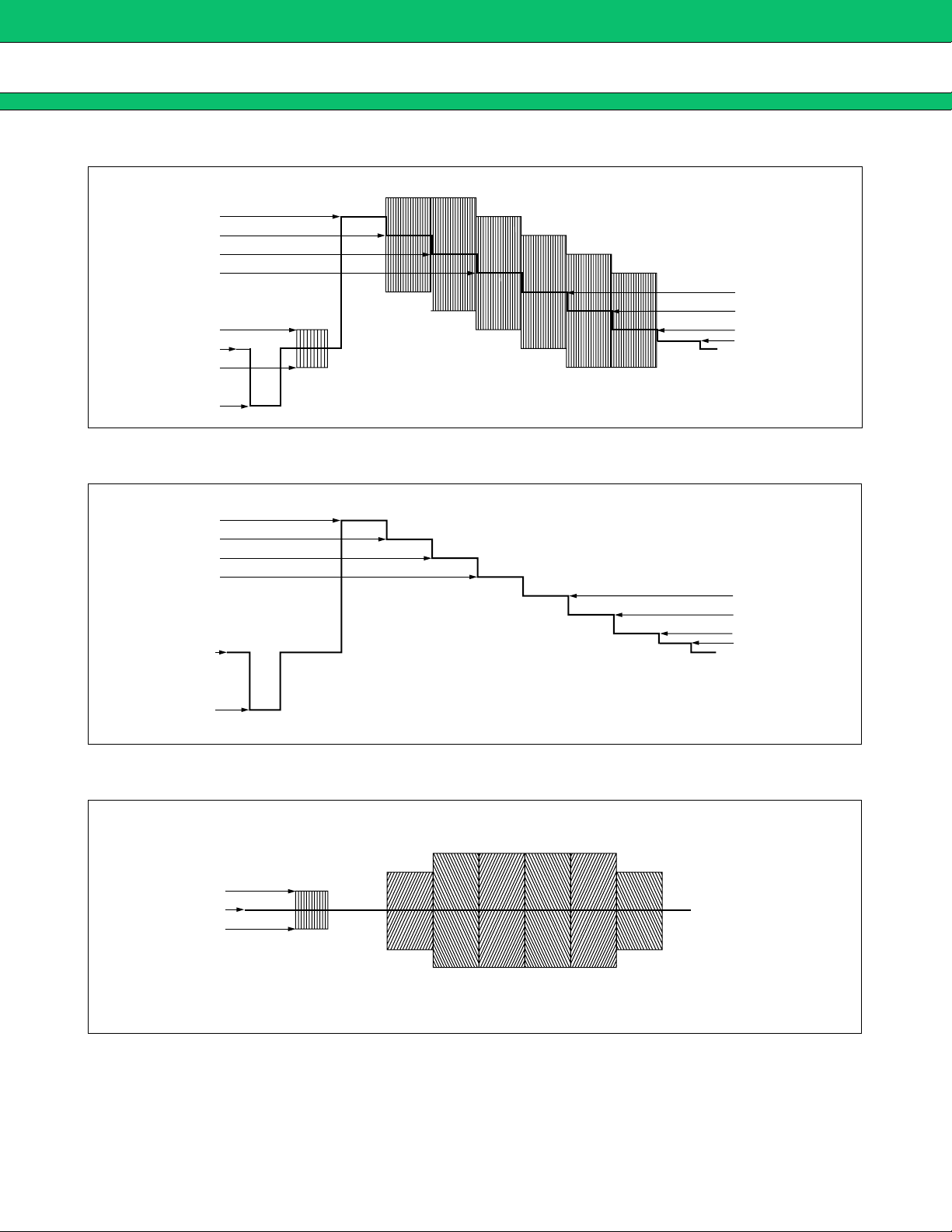
•
NTSC/PAL Horizontal Timing
Video signal
Horizontal sync signal
Horizontal retrace blanking
interval
MB90050
Burst flag
Equalizing pulse
Cut-in pulse
HBLKE
BSTE
BSTS
HPE
EQP1E
HPS
HBLKS
EQP2E
EQP2S
SEP1S
IHCLR
HBLKS
SEP2S
25

MB90050
•
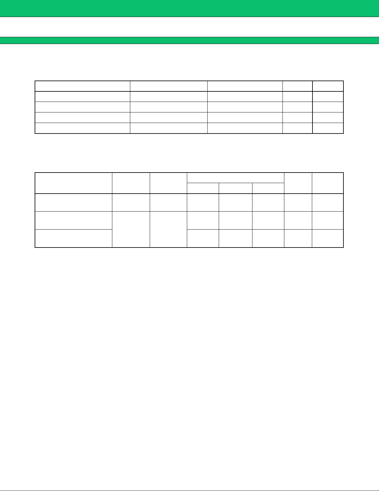
NTSC Vertical Timing
263
· · 18 19 20 · · 258 259 262261260
521 522 523 524 525 123 4567
· · 280 281 282 · · 521 522 525524523 1
VBLKS VPS VPE EQPE VBLKE VBLKS VPS
VBLKS EQPE VBLKE VBLKS VPSVPS VPE
259 260 261 262 263 264 265 266 267 268 269 270
26
Composite video signal
Horizontal scanning line No.
Vertical sync interval
Vertical retrace blanking interval
Even-numbered field
Equalizing pulse interval
numbered field
Composite video signal
Horizontal scanning line No.
Vertical sync interval
Vertical retrace blanking interval
Odd
Equalizing pulse interval

•
PAL Vertical Timing
MB90050
· · 22 23 24 · · 308 309 312311310 313
VPS
VBLKS
· · 335 336 337 · · 621 622 625624623 1
318
VPS
EQPE VBLKSBSTE VPE
· · 22 23 24 · · 308 309 312311310 313
VPS
· · 335 336 337 · · 621 622 625624623 1
318
VPS
EQPE VBLKSVPE
621 622 623 624 625 123 4567
Color burst phase
Composite video signal
Horizontal scanning line No.
Vertical sync interval
First field
Vertical retrace blanking interval
VBLKS VPS VPE BSTS VBLKE BSTE
BSTE EQPE
309 310 311 312 313 314 315 316 317 319 320
Color burst phase
Composite video signal
Horizontal scanning line No.
Equalizing pulse interval
Second field
Vertical sync interval
VBLKS VPS BSTS VBLKE BSTE
621 622 623 624 625 123 4567
Vertical retrace blanking interval
Equalizing pulse interval
Color burst phase
Composite video signal
Horizontal scanning line No.
Vertical sync interval
Third field
Vertical retrace blanking interval
Equalizing pulse interval
VBLKS VPS VPE VBLKE
BSTE EQPE, BSTS BSTE, VBLKS
309 310 311 312 313 314 315 316 317 319 320
Color burst phase
Composite video signal
Fourth field
• The arrows marks indicate the phase of color subcarrier. (↑ : +135°, ↓ : −135°)
BSTE, VBLKS VPS BSTS VBLKE BSTE
Notes : • ◆ indicates the HSYNC positions in the equalizing pulse intends.
Horizontal scanning line No.
Vertical sync interval
Vertical retrace blanking interval
Equalizing pulse interval
27

MB90050
COMMAND LIST
■
Com-
mand
15 to 1211109876543210
no.
0 0000 AY3 AY2 AY1 AY0 FL 0 AX5 AX4 AX3 AX2 AX1 AX0
1 0001 MS1 MS0 MM1 MM0 MB3 MB2 MB1 MB0 MC3 MC2 MC1 MC0
2 0010 MR MG MBL M8 M7 M6 M5 M4 M3 M2 M1 M0
3 0011 LHS LW2 LW1 LW0 LFD LFC LFB LFA LF3 LF2 LF1 LF0
4 0100LDS0LG1LG0LDLELM1LM0L3L2L1L0
5-001010000SDSUDS0DSP0000
5-1010101FM1FM0BT1BT0BD1BD00000
5-2 0101 1 0 0 Y8 Y7 Y6 Y5 Y4 Y3 Y2 Y1 Y0
5-3 0101 1 1 0 X8 X7 X6 X5 X4 X3 X2 X1 X0
Command code/data
Function
VRAM write
address setting
Character data setting 1
Character data setting 2
Line control data
setting 1
Line control data
setting 2
Screen output
control 1
Screen output
control 1
Vertical display
position control
Horizontal display
position control
6-0011000000HB2HB1HB00HA2HA1HA
6-101100100BH3BH2BH1BH0BS3BS2BS1BS0
6-2 0110 1 0 TC HC TC3 TC2 TC1 TC0 HC3 HC2 HC1 HC0
6-3 0110 1 1 GF GC GF3 GF2 GF1 GF0 GC3 GC2 GC1 GC0
7-3011111100000U3U2U1U0
8-1 1000 0 1 SD1 SD0 SM7 SM6 SM5 SM4 SM3 SM2 SM1 SM0
8-21000101SBL0SH2SH1SH00000
9-0 1001 0 0 SY9 SY8 SY7 SY6 SY5 SY4 SY3 SY2 SY1 SY0
9-1 1001 1 0 SX9 SX8 SX7 SX6 SX5 SX4 SX3 SX2 SX1 SX0
Character vertical
size control
Shaded
background frame
color control
Transparent/semitransparent colors
control
Graphic color
control
Screen background
control
Sprite character
control 1
Sprite character
control 2
Sprite character
control 3
Sprite character
control 4
(Continued)
28

MB90050
(Continued)
Command
15 to 1211109876543210
no.
11-0 1011 0 0 FDS FDC MC NP2 NP1 NP0 IN1 IN0 IE1 IE0 Sync control 1
11-1 1011 0 1 0 0 VIX HIX 0 0 VHE HE 0 0 Sync control 2
11-3 1011 1 1 0 0 0 H2 H1 H0 0 F2 F1 F0 Sync detection control
12-0 1100 0 0 STO BUO VSO HSO CSO VBO FDO DHO DBO DCO Output pin control 1
12-1 1100 0 1 STX BUX VOX HOX COX VBX FDX DHX DBX DCX Output pin control 2
12-2 1100 1 0 STU BUU VSU HSU CSU VBU FDU 0 0 0 Output pin control 3
12-3 1100 1 1 CKO FSO CKS FSS 0 0 PO3 PO2 PO1 PO0 Output pin control 4
13-0 1101 0 0 0 PLV PLY PLC PLM PLD PL3 PL2 PL1 PL0 Color palette setting
13-1 1101 1 AA2 AA1 AA0 0 0 AD5 AD4 AD3 AD2 AD1 AD0 Analog level control
14-0 1110 0 0 0 0 0 0 0 FRS 0 0 FA1 FA0 Font RAM setting 1
14-11110010000000FR2FR1FR0Font RAM setting 2
Command code/data
Function
Note : When a reset signal is input (L level signal input to RESET
to command 0) bits (SDS, UDS and DSP) and the output pin control 1 to 4 (command 12-0 to command 12-
3) bits are initialized to “0”.The color palette setting (command 13-0) and analog level control (command
13-1) bits are internally set to their predetermined initial values.The contents of other register bits, VRAM
and font RAM are undefined. After reset input (release) is completed, set all command and f ont RAM settings.
pin) , the screen output control 1 (command 5
29
MB90050
SAMPLE CIRCUIT
■
Composite IN
Video amplifier
clamp circuit
YIN/CIN
Video amplifier
clamp circuit
MB90050
Composite OUT
&
&
VIN
YIN
CIN
VOUT
YOUT
COUT
Buffer circuit
YOUT/COUT
Buffer circuit
Sync
separation
circuit
Control
microcontroller
+ 5 V
+
+ 5 V
+
VSYNCI
HSYNCI
CS
SCLK
SIN
BUSY
AV
CC1
AV
CC2
AV
SS1
AV
SS2
CC
V
V
SS
30
3.3 µH
20 pF
(Approx. 14 MHz)
20 pF
XD
EXD
EXS
XS
NTSC: 14.31818 MHz
PAL : 17.734475 MHz

MB90050-001 FONT DATA (MB90050-001 is typical product. )
■
000 006004003002001 007005
008 00E00C00B00A009 00F00D
010 016014013012011 017015
MB90050
018 01E01C01B01A019 01F01D
020 026024023022021 027025
028 02E02C02B02A029 02F02D
030 036034033032031 037035
038 03E03C03B03A039 03F03D
(Continued)
31

MB90050
040 046044043042041 047045
048 04E04C04B04A049 04F04D
050 056054053052051 057055
058 05E05C05B05A059 05F05D
060 066064063062061 067065
068 06E06C06B06A069 06F06D
070 076074073072071 077075
32
078 07E07C07B07A079 07F07D
(Continued)

080 086084083082081 087085
088 08E08C08B08A089 08F08D
090 096094093092091 097095
MB90050
098 09E09C09B09A099 09F09D
0A0 0A60A40A30A20A1 0A70A5
0A8 0AE0AC0AB0AA0A9 0AF0AD
0B0 0B60B40B30B20B1 0B70B5
0B8 0BE0BC0BB0BA0B9 0BF0BD
(Continued)
33

MB90050
0C0 0C60C40C30C20C1 0C70C5
0C8 0CE0CC0CB0CA0C9 0CF0CD
0D0 0D60D40D30D20D1 0D70D5
0D8 0DE0DC0DB0DA0D9 0DF0DD
0E0 0E60E40E30E20E1 0E70E5
0E8 0EE0EC0EB0EA0E9 0EF0ED
0F0 0F60F40F30F20F1 0F70F5
34
0F8 0FE0FC0FB0FA0F9 0FF0FD
(Continued)

100 106104103102101 107105
108 10E10C10B10A109 10F10D
110 116114113112111 117115
MB90050
118 11E11C11B11A119 11F11D
120 126124123122121 127125
128 12E12C12B12A129 12F12D
130 136134133132131 137135
138 13E13C13B13A139 13F13D
(Continued)
35

MB90050
140 146144143142141 147145
148 14E14C14B14A149 14F14D
150 156154153152151 157155
158 15E15C15B15A159 15F15D
160 166164163162161 167165
168 16E16C16B16A169 16F16D
170 176174173172171 177175
36
178 17E17C17B17A179 17F17D
(Continued)

180 186184183182181 187185
188 18E18C18B18A189 18F18D
190 196194193192191 197195
MB90050
198 19E19C19B19A199 19F19D
1A0 1A61A41A31A21A1 1A71A5
1A8 1AE1AC1AB1AA1A9 1AF1AD
1B0 1B61B41B31B21B1 1B71B5
1B8 1BE1BC1BB1BA1B9 1BF1BD
(Continued)
37

MB90050
(Continued)
1C0 1C61C41C31C21C1 1C71C5
1C8 1CE1CC1CB1CA1C9 1CF1CD
1D0 1D61D41D31D21D1 1D71D5
1D8 1DE1DC1DB1DA1D9 1DF1DD
1E0 1E61E41E31E21E1 1E71E5
1E8 1EE1EC1EB1EA1E9 1EF1ED
1F0 1F61F41F31F21F1 1F71F5
38
1F8 1FE1FC1FB1FA1F9 1FF1FD

ORDERING INFORMATION
■
Part number Package Remarks
MB90050PF
MB90050
48-pin, plastic QFP
(FPT-48P-M15)
39

MB90050
PACKAGE DIMENSION
■
48-pin, plastic QFP
(FPT-48P-M15)
15.30±0.40(.602±.016)SQ
12.00±0.10(.472±.004)SQ
*
37
48
112
0.80(.031)
INDEX
2536
0.32±0.05
(.013±.002)
Note 1) * : These dimensions do not include resin protrusion.
Note 2) Pins width and pins thickness include plating thickness.
Note 3) Pins width do not include tie bar cutting remainder.
0.17±0.06
(.007±.002)
24
13
0.20(.008)
0.10(.004)
0.10(.004)
"A"
M
Details of "A" part
+0.30
2.40
–0.20
(Mounting height)
+.012
.094
–.008
0~8˚
0.85±0.30
(.033±.012)
+0.10
–0.20
0.25
+.004
.010
–.008
(Stand off)
C
2003 FUJITSU LIMITED F48025S-c-3-4
Dimensions in mm (inches)
Note : The values in parentheses are reference values.
40

MB90050
FUJITSU LIMITED
All Rights Reserved.
The contents of this document are subject to change without notice.
Customers are advised to consult with FUJITSU sales
representatives before ordering.
The information, such as descriptions of function and application
circuit examples, in this document are presented solely for the
purpose of reference to show examples of operations and uses of
Fujitsu semiconductor device; Fujitsu does not warrant proper
operation of the device with respect to use based on such
information. When you develop equipment incorporating the
device based on such information, you must assume any
responsibility arising out of such use of the information. Fujitsu
assumes no liability for any damages whatsoever arising out of
the use of the information.
Any information in this document, including descriptions of
function and schematic diagrams, shall not be construed as license
of the use or exercise of any intellectual property right, such as
patent right or copyright, or any other right of Fujitsu or any third
party or does Fujitsu warrant non-infringement of any third-party’s
intellectual property right or other right by using such information.
Fujitsu assumes no liability for any infringement of the intellectual
property rights or other rights of third parties which would result
from the use of information contained herein.
The products described in this document are designed, developed
and manufactured as contemplated for general use, including
without limitation, ordinary industrial use, general office use,
personal use, and household use, but are not designed, developed
and manufactured as contemplated (1) for use accompanying fatal
risks or dangers that, unless extremely high safety is secured, could
have a serious effect to the public, and could lead directly to death,
personal injury, severe physical damage or other loss (i.e., nuclear
reaction control in nuclear facility, aircraft flight control, air traffic
control, mass transport control, medical life support system, missile
launch control in weapon system), or (2) for use requiring
extremely high reliability (i.e., submersible repeater and artificial
satellite).
Please note that Fujitsu will not be liable against you and/or any
third party for any claims or damages arising in connection with
above-mentioned uses of the products.
Any semiconductor devices have an inherent chance of failure. You
must protect against injury, damage or loss from such failures by
incorporating safety design measures into your facility and
equipment such as redundancy, fire protection, and prevention of
over-current levels and other abnormal operating conditions.
If any products described in this document represent goods or
technologies subject to certain restrictions on export under the
Foreign Exchange and Foreign Trade Law of Japan, the prior
authorization by Japanese government will be required for export
of those products from Japan.
F0412
© 2004 FUJITSU LIMITED Printed in Japan
 Loading...