

Page 1

FUJITSU SEMICONDUCTOR
MICROCONTROLLER MANUAL
MICROCONTROLLERS
CM25–10113–1E
F2MC-8L FAMILY
MB89140 SERIES
HARDWARE MANUAL
Page 2

All Rights Reserved.
F2MC-8L FAMILY
MICROCONTROLLERS
MB89140 SERIES
HARDWARE MANUAL
Edition 1.0 February 1995
1995 FUJITSU DEVICES Inc.
Circuit diagrams utilizing Fujitsu products are included as a means of illustrating typical
semiconductor applications. Complete information sufficient for construction purposes
is not necessarily given.
The information contained in this document has been carefully checked and is believed
to be reliable. However, Fujitsu assumes no responsibility for inaccuracies.
The information contained in this document does not convey any license under the
copyrights, patent rights or trademarks claimed and owned by Fujitsu.
Fujitsu reserves the right to change products or specifications without notice.
No part of this publication may be copied or reproduced in any form or by any means, or
transferred to any third party without prior written consent of Fujitsu.
Page 3

PREFACE
The terms in this manual are defined as follows:
(1) A clock cycle is one clock cycle of the oscillation frequency.
(2) A system clock cycle is the clock frequency divided by the gear function (see 2.2). One cycle time of the
system clock varies with the settings of the CS1 and CS0 bits of the SYCC register. With some internal
resources, the gear change will cause changes in operating speed. See 3.4 for details.
iii
Page 4

Table of Contents
1. GENERAL 1-1. . . . . . . . . . . . . . . . . . . . . . . . . . . . . . . . . . . . . . . . . . . . . . . . . . . . . . . . . . . .
1.1 FEA TURES 1-3. . . . . . . . . . . . . . . . . . . . . . . . . . . . . . . . . . . . . . . . . . . . . . . . . . . . . . .
1.2 PRODUCT SERIES 1-5. . . . . . . . . . . . . . . . . . . . . . . . . . . . . . . . . . . . . . . . . . . . . . . .
1.3 BLOCK DIAGRAM 1-7. . . . . . . . . . . . . . . . . . . . . . . . . . . . . . . . . . . . . . . . . . . . . . . . .
1.4 PIN ASSIGNMENT 1-8. . . . . . . . . . . . . . . . . . . . . . . . . . . . . . . . . . . . . . . . . . . . . . . .
1.5 PIN FUNCTION DESCRIPTION 1-10. . . . . . . . . . . . . . . . . . . . . . . . . . . . . . . . . . . .
1.6 HANDLING DEVICES 1-16. . . . . . . . . . . . . . . . . . . . . . . . . . . . . . . . . . . . . . . . . . . . .
2. HARDWARE CONFIGURATION 2-1. . . . . . . . . . . . . . . . . . . . . . . . . . . . . . . . . . . . . . . . .
2.1 CPU 2-3. . . . . . . . . . . . . . . . . . . . . . . . . . . . . . . . . . . . . . . . . . . . . . . . . . . . . . . . . . . .
2.2 MAIN/SUB CLOCK CONTROL BLOCK 2-11. . . . . . . . . . . . . . . . . . . . . . . . . . . . . .
2.3 INTERRUPT CONTROLLER 2-22. . . . . . . . . . . . . . . . . . . . . . . . . . . . . . . . . . . . . .
2.4 I/O PORTS 2-25. . . . . . . . . . . . . . . . . . . . . . . . . . . . . . . . . . . . . . . . . . . . . . . . . . . . . .
2.5 WATCH PRESCALER 2-34. . . . . . . . . . . . . . . . . . . . . . . . . . . . . . . . . . . . . . . . . . . .
2.6 WATCHDOG TIMER RESET 2-36. . . . . . . . . . . . . . . . . . . . . . . . . . . . . . . . . . . . . .
2.7 TIME-BASE TIMER 2-41. . . . . . . . . . . . . . . . . . . . . . . . . . . . . . . . . . . . . . . . . . . . . .
2.8 8-BIT PWM TIMER (TIMER 1) 2-43. . . . . . . . . . . . . . . . . . . . . . . . . . . . . . . . . . . . .
2.9 8/16-BIT TIMER (TIMER 2 AND TIMER 3) 2-48. . . . . . . . . . . . . . . . . . . . . . . . . .
2.10 12-BIT MULTIPUL GENERATOR (MPG, TIMER 4) 2-55. . . . . . . . . . . . . . . . . . .
2.11 8-BIT SERIAL I/O 2-70. . . . . . . . . . . . . . . . . . . . . . . . . . . . . . . . . . . . . . . . . . . . . . . .
2.12 A/D CONVERTER 2-76. . . . . . . . . . . . . . . . . . . . . . . . . . . . . . . . . . . . . . . . . . . . . . .
2.13 BUZZER OUTPUT CIRCUIT 2-83. . . . . . . . . . . . . . . . . . . . . . . . . . . . . . . . . . . . . .
2.14 EXTERNAL INTERRUPT CIRCUIT 2-85. . . . . . . . . . . . . . . . . . . . . . . . . . . . . . . .
3. OPERA TION 3-1. . . . . . . . . . . . . . . . . . . . . . . . . . . . . . . . . . . . . . . . . . . . . . . . . . . . . . . . . .
3.1 CLOCK PULSE GENERATOR 3-3. . . . . . . . . . . . . . . . . . . . . . . . . . . . . . . . . . . . . .
3.2 RESET 3-4. . . . . . . . . . . . . . . . . . . . . . . . . . . . . . . . . . . . . . . . . . . . . . . . . . . . . . . . . .
3.2.1 Reset Operation 3-4. . . . . . . . . . . . . . . . . . . . . . . . . . . . . . . . . . . . . . . . . . . . . . . . . . . . . . . . . . .
3.2.2 Reset Sources 3-5. . . . . . . . . . . . . . . . . . . . . . . . . . . . . . . . . . . . . . . . . . . . . . . . . . . . . . . . . . . .
3.3 INTERRUPT 3-6. . . . . . . . . . . . . . . . . . . . . . . . . . . . . . . . . . . . . . . . . . . . . . . . . . . . .
3.4 LOW-POWER CONSUMPTION MODES 3-8. . . . . . . . . . . . . . . . . . . . . . . . . . . .
3.5 PIN STATES FOR SLEEP, STOP AND RESET 3-9. . . . . . . . . . . . . . . . . . . . . . .
4. INSTRUCTIONS 4-1. . . . . . . . . . . . . . . . . . . . . . . . . . . . . . . . . . . . . . . . . . . . . . . . . . . . . . .
4.1 TRANSFER INSTRUCTIONS 4-3. . . . . . . . . . . . . . . . . . . . . . . . . . . . . . . . . . . . . .
4.2 OPERATION INSTRUCTIONS 4-4. . . . . . . . . . . . . . . . . . . . . . . . . . . . . . . . . . . . .
4.3 BRANCH INSTRUCTIONS 4-5. . . . . . . . . . . . . . . . . . . . . . . . . . . . . . . . . . . . . . . . .
4.4 OTHER INSTRUCTIONS 4-6. . . . . . . . . . . . . . . . . . . . . . . . . . . . . . . . . . . . . . . . . .
4.5 F
2
MC-8L FAMILY INSTRUCTION MAP 4-7. . . . . . . . . . . . . . . . . . . . . . . . . . . . . .
5. MASK OPTIONS 5-1. . . . . . . . . . . . . . . . . . . . . . . . . . . . . . . . . . . . . . . . . . . . . . . . . . . . . . .
APPENDIX App. 1. . . . . . . . . . . . . . . . . . . . . . . . . . . . . . . . . . . . . . . . . . . . . . . . . . . . . . . . . . . .
APPENDIX A I/O MAP App.- 3. . . . . . . . . . . . . . . . . . . . . . . . . . . . . . . . . . . . . . . . . . . . . .
APPENDIX B EPROM SETTING FOR MB89P147 App.- 5. . . . . . . . . . . . . . . . . . . . .
APPENDIX C LIST OF SYSTEM CLOCK CYCLE TIMES WHEN GEAR
CHANGED (SOURCE CLOCK: 8 MHz, 4 MHz) App.- 7. . . . . . . . . .
iv
Page 5

Tables
Table 1-1 Types and Functions of MB89140 Series of Microcontrollers 1-5. . . . . . . . . . . . . . . . . . . . . . . . . . .
Table 1-1 Types and Functions of MB89140 Series of Microcontrollers (Continued) 1-6. . . . . . . . . . . . . . . .
Table 1-2 Pin Function Description 1-10. . . . . . . . . . . . . . . . . . . . . . . . . . . . . . . . . . . . . . . . . . . . . . . . . . . . . . . . .
Table 1-3 Pin for External-ROM 1-13. . . . . . . . . . . . . . . . . . . . . . . . . . . . . . . . . . . . . . . . . . . . . . . . . . . . . . . . . . . .
Table 2-1 Table of Reset and Interrupt Vectors 2-4. . . . . . . . . . . . . . . . . . . . . . . . . . . . . . . . . . . . . . . . . . . . . . .
Table 2-2 Operating State of Low-power Consumption Modes 2-15. . . . . . . . . . . . . . . . . . . . . . . . . . . . . . . .
Table 2-3 Sources of Reset 2-20. . . . . . . . . . . . . . . . . . . . . . . . . . . . . . . . . . . . . . . . . . . . . . . . . . . . . . . . . . . . . . .
Table 2-4 List of Port Functions 2-25. . . . . . . . . . . . . . . . . . . . . . . . . . . . . . . . . . . . . . . . . . . . . . . . . . . . . . . . . . .
Table 2-5 Port register 2-26. . . . . . . . . . . . . . . . . . . . . . . . . . . . . . . . . . . . . . . . . . . . . . . . . . . . . . . . . . . . . . . . . . .
Table 2-6 Relationship between value Set at OUTCR and Duty 2-65. . . . . . . . . . . . . . . . . . . . . . . . . . . . . . .
Table 2-7 Buzzer Output Frequencies
Table 3-1 Interrupt Sources and Interrupt Vectors 3-7. . . . . . . . . . . . . . . . . . . . . . . . . . . . . . . . . . . . . . . . . . . .
Table 3-2 Low-power Consumption Mode at Each Clock Mode 3-8. . . . . . . . . . . . . . . . . . . . . . . . . . . . . . . . .
Table 3-3 Pin State of MB89140 3-9. . . . . . . . . . . . . . . . . . . . . . . . . . . . . . . . . . . . . . . . . . . . . . . . . . . . . . . . . . .
Table 5-1 Mask Options 5-3. . . . . . . . . . . . . . . . . . . . . . . . . . . . . . . . . . . . . . . . . . . . . . . . . . . . . . . . . . . . . . . . . . .
Table 5-2 Model Specifications 5-3. . . . . . . . . . . . . . . . . . . . . . . . . . . . . . . . . . . . . . . . . . . . . . . . . . . . . . . . . . . . .
(at 8.0 MHz of oscillation frequency) 2-84. . . . . . . . . . . . . . . . . . . . . . . . . . . . . . . . . . . . . . . . . . . . . .
v
Page 6

Figures
Fig. 1.1 MB89140 series 1-4. . . . . . . . . . . . . . . . . . . . . . . . . . . . . . . . . . . . . . . . . . . . . . . . . . . . . . . . . . . . . . . . .
Fig. 1.2 Block Diagram 1-7. . . . . . . . . . . . . . . . . . . . . . . . . . . . . . . . . . . . . . . . . . . . . . . . . . . . . . . . . . . . . . . . . . .
Fig. 1.3 Pin Assignment (DIP-64P-M01, MDP-64C-P02) 1-8. . . . . . . . . . . . . . . . . . . . . . . . . . . . . . . . . . . . . .
Fig. 1.4 Pin Assignment (FPT-64P-M06, MDP-64C-P01) 1-9. . . . . . . . . . . . . . . . . . . . . . . . . . . . . . . . . . . . .
Fig. 1.5 Input/Output Circuit Configurations 1-14. . . . . . . . . . . . . . . . . . . . . . . . . . . . . . . . . . . . . . . . . . . . . . . .
Fig. 2.1 Memory Space of MB89140 Series of Microcontrollers 2-3. . . . . . . . . . . . . . . . . . . . . . . . . . . . . . . .
Fig. 2.2 Arrangement of 16-bit Data in Memory 2-5. . . . . . . . . . . . . . . . . . . . . . . . . . . . . . . . . . . . . . . . . . . . . .
Fig. 2.3 Arrangement of 16-bit Data during Execution of Instruction 2-5. . . . . . . . . . . . . . . . . . . . . . . . . . . .
Fig. 2.4 Structure of Processor Status 2-6. . . . . . . . . . . . . . . . . . . . . . . . . . . . . . . . . . . . . . . . . . . . . . . . . . . . .
Fig. 2.5 Rule for Translating Real Addresses at General-purpose Register Area 2-7. . . . . . . . . . . . . . . . .
Fig. 2.6 Register Bank Configuration 2-8. . . . . . . . . . . . . . . . . . . . . . . . . . . . . . . . . . . . . . . . . . . . . . . . . . . . . . .
Fig. 2.7 Memory Map in Various Modes 2-9. . . . . . . . . . . . . . . . . . . . . . . . . . . . . . . . . . . . . . . . . . . . . . . . . . . .
Fig. 2.8 Machine Clock Control Block Diagram 2-11. . . . . . . . . . . . . . . . . . . . . . . . . . . . . . . . . . . . . . . . . . . . .
Fig. 2.9 Interrupt Controller Block Diagram 2-22. . . . . . . . . . . . . . . . . . . . . . . . . . . . . . . . . . . . . . . . . . . . . . . .
Fig. 2.10 Interrupt-processing Flowchart 2-24. . . . . . . . . . . . . . . . . . . . . . . . . . . . . . . . . . . . . . . . . . . . . . . . . . . .
Fig. 2.11 Ports 00 to 07 and 10 to 13 2-28. . . . . . . . . . . . . . . . . . . . . . . . . . . . . . . . . . . . . . . . . . . . . . . . . . . . . .
Fig. 2.12 Ports 14 to 16 2-29. . . . . . . . . . . . . . . . . . . . . . . . . . . . . . . . . . . . . . . . . . . . . . . . . . . . . . . . . . . . . . . . . .
Fig. 2.13 Ports 20 to 23 2-29. . . . . . . . . . . . . . . . . . . . . . . . . . . . . . . . . . . . . . . . . . . . . . . . . . . . . . . . . . . . . . . . . .
Fig. 2.14 Ports 70 and 71 2-30. . . . . . . . . . . . . . . . . . . . . . . . . . . . . . . . . . . . . . . . . . . . . . . . . . . . . . . . . . . . . . . .
Fig. 2.15 Ports 35 to 32, 30 and 17 2-31. . . . . . . . . . . . . . . . . . . . . . . . . . . . . . . . . . . . . . . . . . . . . . . . . . . . . . . .
Fig. 2.16 Port 31 2-32. . . . . . . . . . . . . . . . . . . . . . . . . . . . . . . . . . . . . . . . . . . . . . . . . . . . . . . . . . . . . . . . . . . . . . . .
Fig. 2.17 Ports 40 to 47, 50 to 57 and 60 to 67 2-33. . . . . . . . . . . . . . . . . . . . . . . . . . . . . . . . . . . . . . . . . . . . . .
Fig. 2.18 BZ 2-33. . . . . . . . . . . . . . . . . . . . . . . . . . . . . . . . . . . . . . . . . . . . . . . . . . . . . . . . . . . . . . . . . . . . . . . . . . . .
Fig. 2.19 Watch Prescaler Block Diagram 2-34. . . . . . . . . . . . . . . . . . . . . . . . . . . . . . . . . . . . . . . . . . . . . . . . . .
Fig. 2.20 Watchdog Timer Reset Block Diagram 2-36. . . . . . . . . . . . . . . . . . . . . . . . . . . . . . . . . . . . . . . . . . . . .
Fig. 2.21 Time-base Timer Block Diagram 2-41. . . . . . . . . . . . . . . . . . . . . . . . . . . . . . . . . . . . . . . . . . . . . . . . . .
Fig. 2.22 8-bit PWM Timer (Timer 1) Block Diagram 2-43. . . . . . . . . . . . . . . . . . . . . . . . . . . . . . . . . . . . . . . . .
Fig. 2.23 Timer Operation 2-46. . . . . . . . . . . . . . . . . . . . . . . . . . . . . . . . . . . . . . . . . . . . . . . . . . . . . . . . . . . . . . . .
Fig. 2.24 PWM Pulse Output 2-47. . . . . . . . . . . . . . . . . . . . . . . . . . . . . . . . . . . . . . . . . . . . . . . . . . . . . . . . . . . . . .
Fig. 2.25 8/16-bit Timer Block Diagram 2-48. . . . . . . . . . . . . . . . . . . . . . . . . . . . . . . . . . . . . . . . . . . . . . . . . . . . .
Fig. 2.26 Description Diagram for Internal Clock Mode Operation 2-52. . . . . . . . . . . . . . . . . . . . . . . . . . . . . .
Fig. 2.27 Flow Diagram for Timer Setting 2-52. . . . . . . . . . . . . . . . . . . . . . . . . . . . . . . . . . . . . . . . . . . . . . . . . . .
Fig. 2.28 External Cock Mode Operation Description Diagram 2-53. . . . . . . . . . . . . . . . . . . . . . . . . . . . . . . . .
Fig. 2.29 Operation Diagram when Timer Stop Bit is Used 2-53. . . . . . . . . . . . . . . . . . . . . . . . . . . . . . . . . . . .
Fig. 2.30 MPG Block Diagram 2-56. . . . . . . . . . . . . . . . . . . . . . . . . . . . . . . . . . . . . . . . . . . . . . . . . . . . . . . . . . . .
Fig. 2.31 Transition of DTTI Input 2-59. . . . . . . . . . . . . . . . . . . . . . . . . . . . . . . . . . . . . . . . . . . . . . . . . . . . . . . . . .
Fig. 2.32 Outline of PWM Output 2-63. . . . . . . . . . . . . . . . . . . . . . . . . . . . . . . . . . . . . . . . . . . . . . . . . . . . . . . . . .
Fig. 2.33 Description of PWM Output Operation 2-63. . . . . . . . . . . . . . . . . . . . . . . . . . . . . . . . . . . . . . . . . . . . .
Fig. 2.34 Flowchart of PWM Operation 2-64. . . . . . . . . . . . . . . . . . . . . . . . . . . . . . . . . . . . . . . . . . . . . . . . . . . . .
Fig. 2.35 Outline of MPG Output 2-67. . . . . . . . . . . . . . . . . . . . . . . . . . . . . . . . . . . . . . . . . . . . . . . . . . . . . . . . . .
Fig. 2.36 Description of PPG Output Operation 2-67. . . . . . . . . . . . . . . . . . . . . . . . . . . . . . . . . . . . . . . . . . . . . .
Fig. 2.37 Flowchart of PPG Operation 2-68. . . . . . . . . . . . . . . . . . . . . . . . . . . . . . . . . . . . . . . . . . . . . . . . . . . . . .
Fig. 2.38 8-bit Serial I/O Block Diagram 2-70. . . . . . . . . . . . . . . . . . . . . . . . . . . . . . . . . . . . . . . . . . . . . . . . . . . .
Fig. 2.39 Shift Start/Stop Timing 2-74. . . . . . . . . . . . . . . . . . . . . . . . . . . . . . . . . . . . . . . . . . . . . . . . . . . . . . . . . . .
Fig. 2.40 Input/Output Shift Timing 2-75. . . . . . . . . . . . . . . . . . . . . . . . . . . . . . . . . . . . . . . . . . . . . . . . . . . . . . . . .
Fig. 2.41 A/D Comverter Block Diagram 2-76. . . . . . . . . . . . . . . . . . . . . . . . . . . . . . . . . . . . . . . . . . . . . . . . . . . .
Fig. 2.42 Buzzer Output Circuit Block Diagram 2-83. . . . . . . . . . . . . . . . . . . . . . . . . . . . . . . . . . . . . . . . . . . . . .
Fig. 2.43 External Interrupt Circuit Block Diagram 2-85. . . . . . . . . . . . . . . . . . . . . . . . . . . . . . . . . . . . . . . . . . .
Fig. 3.1 Clock Pulse Generator 3-3. . . . . . . . . . . . . . . . . . . . . . . . . . . . . . . . . . . . . . . . . . . . . . . . . . . . . . . . . . .
Fig. 3.2 Outline of Reset Operation 3-4. . . . . . . . . . . . . . . . . . . . . . . . . . . . . . . . . . . . . . . . . . . . . . . . . . . . . . . .
Fig. 3.3 Reset Vector Structure 3-4. . . . . . . . . . . . . . . . . . . . . . . . . . . . . . . . . . . . . . . . . . . . . . . . . . . . . . . . . . .
Fig. 3.4 Interrupt-processing Flowchart 3-6. . . . . . . . . . . . . . . . . . . . . . . . . . . . . . . . . . . . . . . . . . . . . . . . . . . . .
vi
Page 7

1. GENERAL
1.1 FEATURES 1-3. . . . . . . . . . . . . . . . . . . . . . . . . . . . . . . . . . . . .
1.2 PRODUCT SERIES 1-5. . . . . . . . . . . . . . . . . . . . . . . . . . . . .
1.3 BLOCK DIAGRAM 1-7. . . . . . . . . . . . . . . . . . . . . . . . . . . . . .
1.4 PIN ASSIGNMENT 1-8. . . . . . . . . . . . . . . . . . . . . . . . . . . . . .
1.5 PIN FUNCTION DESCRIPTION 1-10. . . . . . . . . . . . . . . . .
1.6 HANDLING DEVICES 1-16. . . . . . . . . . . . . . . . . . . . . . . . .
Page 8

GENERAL
The MB89140 series of single-chip microcontrollers use the F2MC-8L CPU core to enable high-speed processing at low voltages, and features a 25 segment VFD (V acuum Fluorescent Display) driver . They contain resources such as timers, a serial interface, an A/D converter and an external interrupt input to provide a wide
variety of applications for commercial and industrial equipment, including portable equipment.
The MB89140 series of single-chip microcontrollers has twenty-five V
which makes it suitable for VFD display application such as microwave oven, fan heater, room air conditioner ,
dashboard controller, and so on.
-40VP-channel high voltage ports
CC
1.1 FEATURES
• Minimum instruction execution time: 0.5 µs (at oscillation frequency of 8 MHz)
• CPU core as commonly used for MB89860 series
Multiplication and division instructions
–Instruction system best for controller
• Operation at low voltage (A/D converter unused)
• 25 segment VFD (Vacuum Fluorescent Display) driver.
• Low current dissipation (applicable to dual-circuit clock)
• Internal high-withstand-voltage ports
• 5 timers
–8-bit PWM timer (available as reload timer)
–12-bit MPG timer (available as PPG output, PWM output and reload timer)
–8/16-bit timer/counter (available as two 8-bit timers)
–21-bit time-base counter
16-bit operation
Instruction test and branch instruction
Bit handling instruction, etc.
• Single serial interface
–Transfer direction selected for communication with various equipment
• A/D converter
–Successive approximation type with 10-bit resolution
• 2-channel external interrupt input
–Two channels can be selected independently to cancel the low-power consumption modes (selectable
from rising edge, falling edge, or both edges).
–The INT1 can be applied from –0.7 V to 7.0 V (N-channel open drain).
• Low-power consumption modes
–Stop mode (The oscillation stops to minimize current consumption.)
–Sleep mode (The CPU stops to cut current consumption to about 30% of normal.)
• Reset output or power-on reset available option can be selected.
• Packages
–SDIP-64 and QFP-64 packages
1-3
Page 9

(Planned)
MB89144
ROM 12K
RAM 256
(Under development)
MB89145
ROM 16K
RAM 512
Fig. 1.1 MB89140 series
GENERAL
(Planned)
MB89146
Memory capacity
Small Large
ROM 24K
RAM 768
(Under development)
MB89147
ROM 32K
RAM 1K
1-4
Page 10
GENERAL
1.2 PRODUCT SERIES
Table 1-1 lists the types and functions of the MB89140 series of microcontrollers.
Table 1-1 Types and Functions of MB89140 Series of Microcontrollers
Model Name MB89144 MB89145 MB89146 MB89147
Classification
ROM capacity 12K × 8 bit 16K × 8 bit 24K × 8 bit 32K × 8 bit
RAM capacity 256 × 8 bit 512 × 8 bit 768 × 8 bit 1K × 8 bit
Number of basic instructions 136
Instruction bit length 8 bits
Instruction length 1 to 3 bytes
CPU functions Data bit length 1, 8, 16 bits
Minimum instruction execution time 0.5 µs/8 MHz to 8.0 µs/8 MHz and 61 µs/32.768 kHz
Interrupt processing time 4.5 µs/8 MHz to 72.0 µs/8 MHz and 562.5 µs/32.768 kHz
High-withstand-voltage output port 8 (P60 to P67 for large current)
(P-channel open drain) 16 (P40 to P47, P50 to P57 for small current)
Buzzer output 1 (Large current)
(P-channel open drain, high-withstand-voltage)
Output port (CMOS) 4 (P20 to P23)
Port Input port (CMOS) 2 (P70 to P71; serve as X0A and X1A pins when two
I/O port (CMOS) 23 (P00 to P07, P10 to P17, P30, P32 to P37)
I/O port (N-channel open drain) 1 (P31)
Total 55
Mass-produced product
(Mask ROM product)
Note: The above times vary with gear function.
clocks used)
MB89P147
MB89W147
OTPROM/
EPROM product
Internal
32K × 8 bits
Internal
1K × 8 bits
MB89PV140
Piggyback/evaluation
product for evaluation
and development
External 32K × 8
bits (Piggyback)
Internal
1024 × 8 bits
VFD 25 segment
Time-base timer
8-bit PWM timer
(Timer 1)
12-bit MPB timer 12-bit resolution reload timer operation (toggle output possible)
(Timer 4) 12-bit resolution PPG operation (minimum resolution: 0.5 µs at oscillation frequency of 8.0 MHz and
8/16-bit timer/counter 8/16-bit timer operation (operating clock, internal clock and external trigger). See 2.2 for details.
(Timers 2 and 3) 8/16-bit event counter operation (selectable from rising edge, falling edge, or both edges)
Capable of generating four internal pulses of 0.26 ms, 0.51 ms, 1.02 ms and 0.524 s
(at oscillation frequency of 8.0 MHz)
8-bit timer operation (toggle output possible, 1, 2, 8 or 16 system clock cycles of operating clock)
8-bit resolution PWM operation (conversion cycle: 128 µs to 2.0 ms at oscillation frequency of 8.0 MHz
and maximum gear speed)
12-bit resolution PWM operation (maximum conversion cycle: 2048.4 µs to 16.4 ms
maximum gear speed)
1-5
Page 11
GENERAL
Table 1-1 Types and Functions of MB89140 Series of Microcontrollers (Continued)
Model Name MB89144 MB89145 MB89146 MB89147
Serial I/O
A/D converter
External interrupt Interrupt mode selectable from rising edge, falling edge, or both edge. Analog noise filter built in
Standby mode Sleep, Stop and Watch mode
Process CMOS
Package DIP-64P-M01 (SDIP-64)/FPT-64P-M06 (QFP64)
Operating voltage 2.7 V to 6.0 V* 2.7 V to 6.0 V
8-bit length 1 channel
Transfer clock (external, 4, 8 or 16 system clock cycles)
10-bit resolution, 12 channels
A/D conversion mode (conversion time: 16.5 µs at 8 MHz and maximum gear speed)
Sense mode (conversion time: 9.0 µs at 8 MHz and maximum gear speed)
Continuous start by external activation or internal timer
2 independent channels (edge selection, interrupt vector, interrupt source flag)
For releasing Stop/Sleep modes (edge detection possible in Stop mode)
MB89P147
MB89W147
MB89PV140
MDP-64C-P02/
MQP-64C-P01
* Operating voltage varies depending to the condition such as frequency or others.
1-6
Page 12
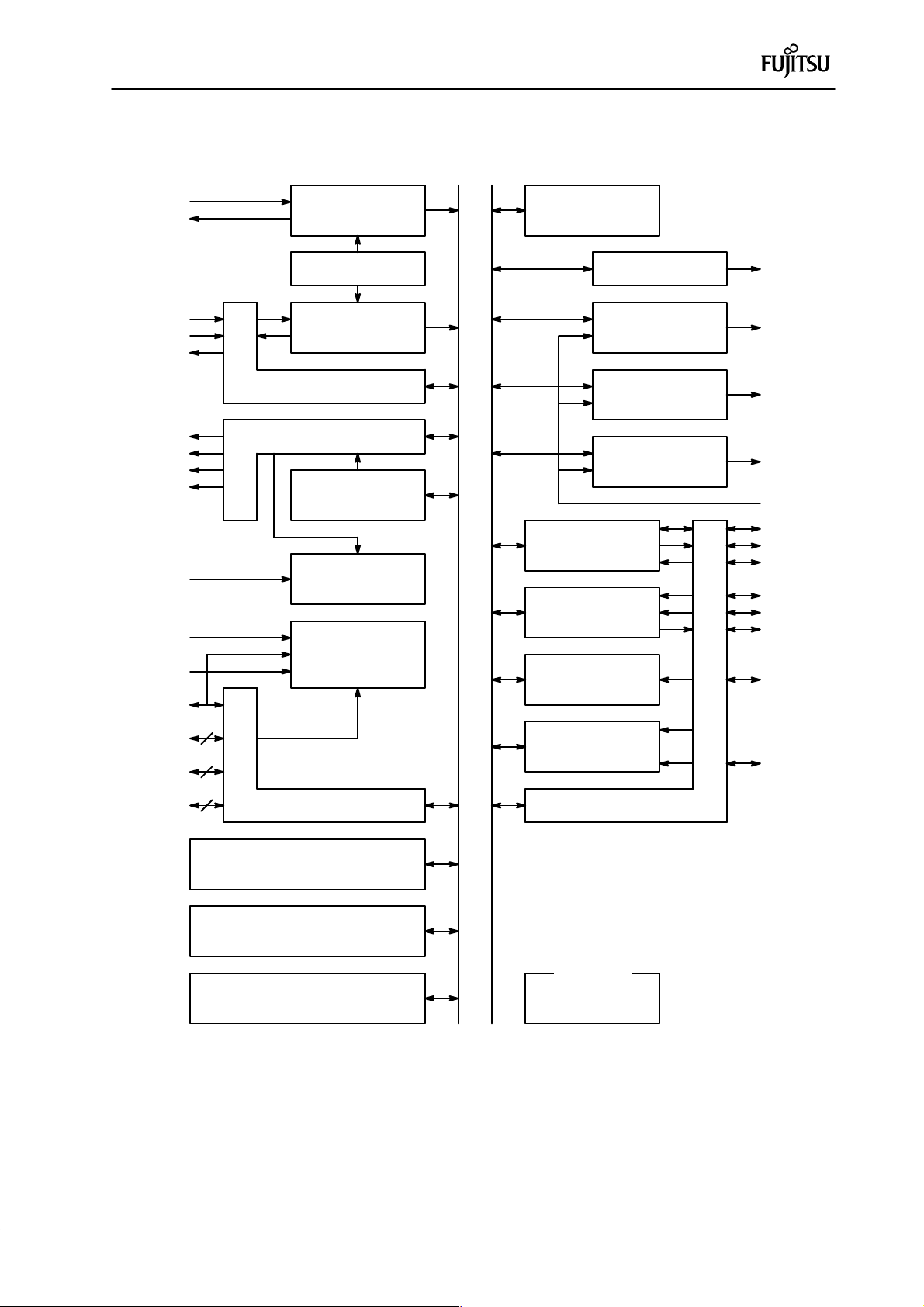
1.3 BLOCK DIAGRAM
GENERAL
Internal bus
X0
X1
P70, P71
X0A
X1A
P23/WDG
P22
P21/PWO0
P20
MODA
AV
CC
AV
SS
Port
7
Port
2
Main clock oscillator
(Max. 8 MHz)
Clock control
Sub clock oscillator
(32.768 kHz)
CMOS input port
CMOS output port
8-bit PWM timer
Mode control
10-bit A/D converter
Time-base timer
High-withstand-voltage
High-withstand-voltage
High-withstand-voltage
8-bit serial
12-bit MPG
8/16-bit timer/counter
Buzzer
port 6
port 5
port 4
Port
3
BZ
P60 to P67
P50 to P57
P40 to P47
VFD
P32/SCK
P33/SO
P34/SI
P30/TRG/INT0
P37/DTTI
P3/PWO1
P35/EC
P17/ADST
P14 to P16
P13/ANB to
P10/AN8
P07/AN7 to
P00/AN0
4
Port
4
0/1
8
CMOS output port
(Max. 512 × 8 bit )
F
(Max. 16 K × 8 bit)
RAM
2
MC-8L
CPU
ROM
External interrupt
Fig. 1.2 Block Diagram
input
CMOS I/O port
Other pins
VCC, V
SS
P31/INT1
1-7
Page 13
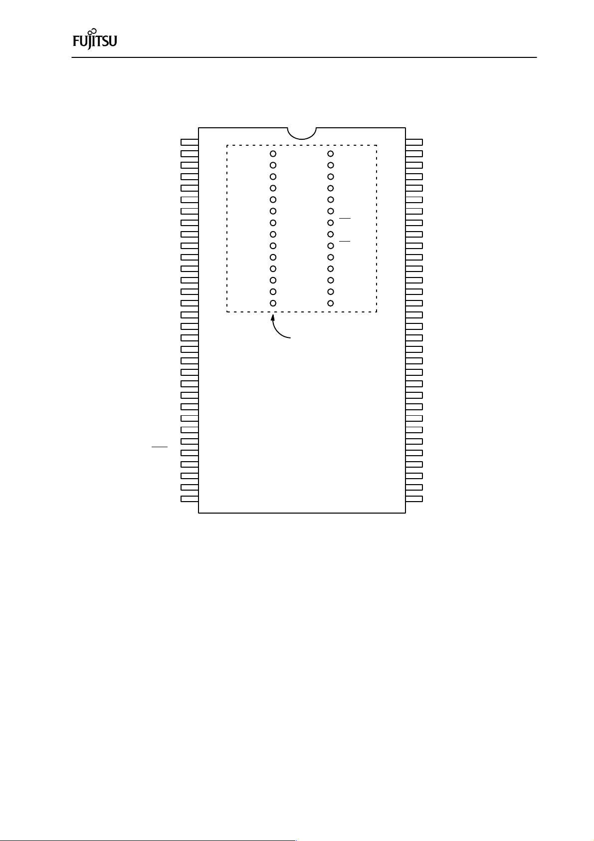
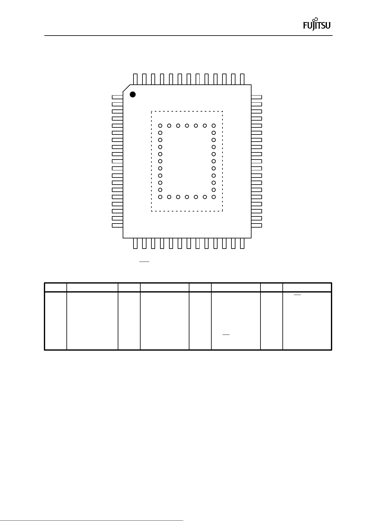
1.4 PIN ASSIGNMENT
GENERAL
TOP VIEW
BZ ←
P67 ←
P66 ←
P65 ←
P64 ←
P63 ←
P62 ←
P61 ←
P60 ←
VFD →
P57 ←
P56 ←
P55 ←
P54 ←
P53 ←
P52 ←
P51 ←
P50 ←
P47 ←
P46 ←
P45 ←
P44 ←
P43 ←
P42 ←
P41 ←
P40 ←
P23/WDG ←
RST
↔
MODA →
X0 →
X1 ←
V
←
SS
1
2
3
4
5
6
7
8
9
10
11
12
13
14
15
16
17
18
19
20
21
22
23
24
25
26
27
28
29
30
31
32
A15/VAA
A12
A7
A6
A5
A4
A3
A2
A1
A0
O1
O2
O3
V
SS
65
66
67
68
69
70
71
72
73
74
75
76
77
78
92
91
90
89
88
87
86
85
84
83
82
81
80
79
Items in dotted lines
are only available for
the MB89PV140.
V
CC
A14
A13
A8
A9
A11
OE
A10
CE
O8
O7
O6
O5
O4
64
63
62
61
60
59
58
57
56
55
54
53
52
51
50
49
48
47
46
45
44
43
42
41
40
39
38
37
36
35
34
33
← V
CC
← AV
CC
← AV
SS
↔ P00/AN0
↔ P01/AN1
↔ P02/AN2
↔ P03/AN3
↔ P04/AN4
↔ P05/AN5
↔ P06/AN6
↔ P07/AN7
↔ P10/AN8
↔ P11/AN9
↔ P12/ANA
↔ P13/ANB
↔ P14
↔ P15
↔ P16
↔ P17/ADST
↔ P30/INT0/TRG
↔ P31/INT1
↔ P32/SCK
↔ P33/SO
↔ P34/SI
↔ P35/EC
↔ P36/PWO1
↔ P37/DTTI
→ P20
→ P21/PWO0
→ P22
← P70/X0A
↔ P71/X1A
The SH-DIP64 cautions are as follows:
• Pins 33 and 34 serve as input-only ports when used as general-purpose ports.
• Pin 28 serves as an output pin when the reset output option is selected.
• P07 to P00 and P13 to P10 serve as analog input ports after reset. When using them as port inputs, registers
PCR0 and PCR1 must be set.
Fig. 1.3 Pin Assignment (DIP-64P-M01, MDP-64C-P02)
1-8
Page 14
GENERAL
P61
P60
VFD
P57
P56
P55
P54
P53
P52
P51
P50
P47
P46
P45
P44
P43
P42
P41
P40
P63 P65 P67 V
CC
AV
SS
P00/ P02/
P62 P64 P66 BZ AV
CC
AN0 AN2
64 63 62 61 60 59 58 57 56 55 54 53 52
1
TOP VIEW
2
3
4
84 83 82 81 80 79 78
5
6
7
8
9
10
11
12
13
14
85
86
87
88
89
90
91
92
93
77
76
75
74
73
72
71
70
69
15
16
17
18
19
94 95 96 65 66 67 68
Items in dotted lines are only
available for the MB89PV140.
20 21 22 23 24 25 26 27 28 29 30 31 32
P01
/AN1
51
50
49
48
47
46
45
44
43
42
41
40
39
38
37
36
35
34
33
P03/AN3
P04/AN4
P05/AN5
P06/AN6
P07/AN7
P10/AN8
P11/AN9
P12/ANA
P13/ANB
P14
P15
P16
P17/ADST
P30/INT0/TRG
P31/INT1
P32/SCK
P33/SO
P34/SI
P35/EC
P23 MODA X1 P71/ P22 P20 P36/
/WDG X1A PWO1
RST
X0 V
P70/ P21/ P37/
SS
X0A PWO0 DTTI
Pin Symbol Pin Symbol Pin Symbol Pin Symbol
65 N.C. 73 A2 81 N.C. 89 OE
66 A15/V
PP
74 A1 82 O4 90 N.C.
67 A12 75 A0 83 O5 91 A11
68 A7 76 N.C. 84 O6 92 A9
69 A6 77 O1 85 O7 93 A8
70 A5 78 O2 86 O8 94 A13
71 A4 79 O3 87 CE
72 A3 80 V
SS
88 A10 96 V
95 A14
CC
Fig. 1.4 Pin Assignment (FPT-64P-M06, MDP-64C-P01)
1-9
Page 15
GENERAL
1.5 PIN FUNCTION DESCRIPTION
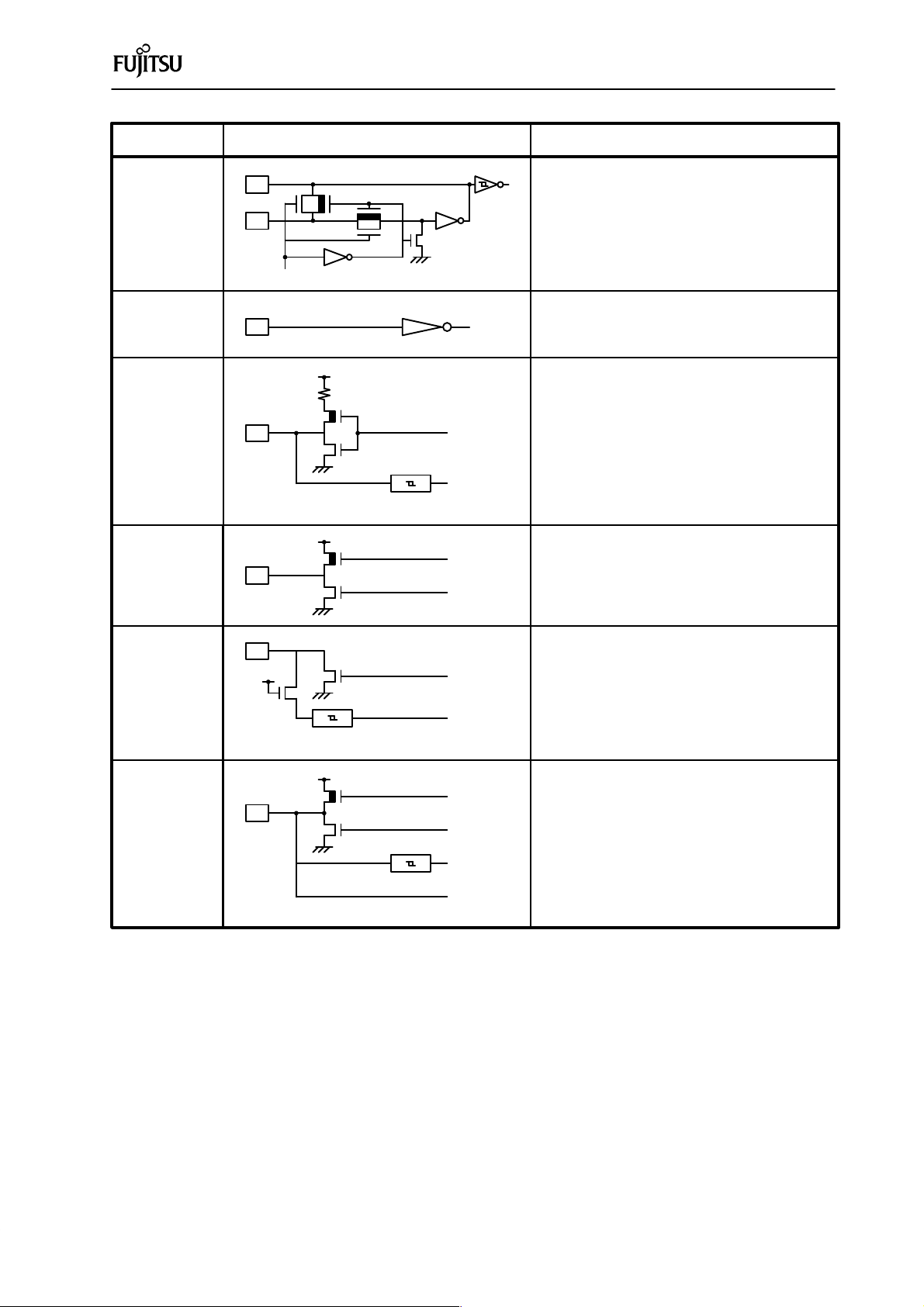
Table 1-2 and NO TAG lists the pin function and Figure 1.3 shows the input/output circuit configurations.
Table 1-2 Pin Function Description
Pin No.
SDIP
30 23 X0 Used for main clock oscillation
31 24 X1
29 22 MODA B Usually connected to V
28 21 RST
54 to 61 47 to 54 to F
46 39 P17/ADST I Input is hysteresis type containing a noise filter. This port also serves as an
47 to 49 40 to 42 P16 to P14 I
QFP
from this pin according to the internal source. The internal circuit is initial-
Pin Name
P07/AN7
P00/AN0
Circuit
type
A A crystal resonator should be used.
Used for input of operation mode select signals
. This pin serves as the VPP pin for EPROM-
mounted models.
Used for input/output of reset signals
Consists of an N-channel open-drain output with a pull-up resistor and
C hysteresis input. When the reset on option is selected, a Low level is output
ized at input of a Low level. A noise canceler is built in.
General-purpose I/O ports
Input is hysteresis type containing a noise filter. Although these ports also
serves as analog input pins, analog input does not pass through the noise
filter for hysteresis input.
General-purpose I/O port
external start pin for the A/D converter.
General-purpose I/O ports
Input is hysteresis type containing a noise filter.
SS
Function
P13/ANB
50 to 53 43 to 46 to F
P10/AN8
34 27 X0A/P70 A/J pin by the mask option. When using as a general-purpose input pin, input
33 26 X1A/P71 A/J pin by the mask option. When using as a general-purpose input pin, input
35 28 P22 D General-purpose output port
27 20 P23/WDG D
36 29 P21/PWO0 D
37 30 P20 D General-purpose output port
General-purpose I/O ports
Input is hysteresis type containing a noise filter. Although these ports serve
as analog input pins, analog input does not pass through the noise filter for
hysteresis input.
Can be selected as a general-purpose input port or sub-clock generating
is hysteresis type containing a noise filter.
Can be selected as a general-purpose input port or sub-clock generating
is hysteresis type containing a noise filter.
General-purpose output port
This port also serves as a watchdog output pin
General-purpose output port
This port also serves as a PWM output pin for the 8-bit PWM timer.
(see 2.2 for watch dog timer).
1-10
Page 16
GENERAL
Table 1-2 Pin Function Description (Continued)
Pin No.
SDIP
38 31 P37/DTTI I
39 32 P36/PWO1 I Input is hysteresis type containing a noise filter. This port also serves as a
40 33 P35/EC I Input is hysteresis type containing a noise filter . This port also serves as an
41 34 P34/SI I Input is hysteresis type containing a noise filter. This port also serves as an
42 35 P33/SO I Input is hysteresis type containing a noise filter. This port also serves as a
43 36 P32/SCK I Input is hysteresis type containing a noise filter . This port also serves as a
QFP
Pin Name
Circuit
type
Function
General-purpose I/O port
Input is hysteresis type containing a noise filter. When overcurrent is
detected, the external rising or falling edge can be input to inactivate the
12-bit MPG output.
General-purpose I/O port
12-bit MPG output pin.
General-purpose I/O port
external clock input pin for the 8/16-bit timer/counter.
General-purpose I/O port
external clock input pin for the 8-bit timer/counter.
General-purpose I/O port
serial data output pin for the 8-bit serial interface.
General-purpose I/O port
serial transfer clock pin for the 8-bit serial interface.
General-purpose I/O port
44 37 P31/INT1 E
45 38 P30/INT0/TRG I
1 58 BZ H This pin also serves as a P-channel high-withstand-voltage open-drain
19 to 26 12 to 19 P47 to P40 G Two types of microcontrollers are provided: one has a pull-down resistor
11 to 18 4 to 11 P57 to P50 G Two types of microcontrollers are provided: one has a pull-down resistor
2 to 9 59 to 2 P67 to P60 G Two types of microcontrollers are provided: one has a pull-down resistor
10 3 VFD — This pin serves as an NC pin for microcontrollers without a pull-down resistor
Consists of an N-channel open-drain output and hysteresis input containing
a noise filter. This port also serves as an external interrupt pin. Interrupt
input is also hysteresis type containing a noise filter.
General-purpose I/O port
Input is hysteresis type containing a noise filter. This port can also be used
as an external interrupt pin or MPG trigger input pin. Interrupt input is also
hysteresis type containing a noise filter.
Used for buzzer output only
output port.
P-channel high-withstand-voltage open drain output ports for small current
between these ports and the VFD pin, and the other does not.
P-channel high-withstanding-voltage open drain output ports for small current
between these ports and the VFD pin, and the other does not.
P-channel high-withstand-voltage open-drain output ports for large current
between these ports and the VFD pin, and the other does not.
Used for voltage supply connected to pull-down resistors for ports 4, 5 and 6
and the MB89PV140 microcontroller.
1-11
Page 17

GENERAL
Table 1-2 Pin Function Description (Continued)
Pin No.
SDIP
SDIP
64 57 V
32 25 V
63 56 AV
62 55 AV
Pin Name
CC
SS
CC
SS
Circuit
type
Function
— Used for power supply
— Used for power supply (GND)
— Used for power supply for A/D converter
Used for power supply for A/D converter
—
Must be used at same potential as V
SS
pin
1-12
Page 18
GENERAL
Table 1-3 Pin for External-ROM
Pin No.
SDIP QFP
65 66 V
66 67 A12
67 68 A7
68 69 A6
69 70 A5
70 71 A4 Output Address-output pins
71 72 A3
72 73 A2
73 74 A1
74 75 A0
75 77 01
76 78 02 Input Data-input pins
77 79 03
78 80 V
79 82 04
80 83 05
81 84 06 Input Data-input pins
82 85 07
83 86 08
Pin Name
PP
SS
Circuit
type
Output High-level output pin
Output Power (GND) pin
Function
84 87 CE
85 88 A10 Output Address-output pin
86 89 OE
87 91 A11
88 92 A9 Output Address-output pins
89 93 A8
90 94 A13 Output Address-output pin
91 95 A14 Output Address-output pin
92 96 V
CC
Output Chip-enable pin for ROM
A High level is output in the standby mode.
Output Output-enable pin for ROM
A Low level is always output.
Output Power pin for EPROM
1-13
Page 19
GENERAL
Classification Circuit Remarks
X1
• Feedback resistor: About 2 MΩ
X0
A
Standby control signal
B
R
Pch
• CMOS input
• Output pull-up resistor (Pch): About 50 kΩ (5 V)
• CMOS hysteresis input (with noise filter)
C
Nch
Hysteresis input (with noise filter)
Pch
D
Nch
• CMOS output
• N-ch open drain output
• CMOS hysteresis input (with noise filter)
E
Nch
Hysteresis input (with noise filter)
Pch
Nch
• CMOS output
• CMOS hysteresis input (with noise filter; analog
input excluded)
F
Port
Hysteresis input (with noise filter)
Analog input
Fig. 1.5 Input/Output Circuit Configurations
1-14
Page 20
GENERAL
Classification Circuit Remarks
R
Pch
G
VFD
Pch
H
Pch
Nch
I
Port
Hysteresis input (with noise filter)
J
Hysteresis input (with noise filter)
Port
• P-channel high-withstand-voltage open-drain
output
• Microcontrollers with and without pull-down resis
tor provided (excluding MB89V140
microcontroller)
• P-channel high-withstand-voltage open-drain
output
• CMOS output
• CMOS hysteresis input (with noise filter)
• The pull-up resistor is optional.
• CMOS hysteresis input (with noise filter)
Fig. 1.5 Input/Output Circuit Configurations (Continued)
1-15
Page 21
1.6 HANDLING DEVICES
(1) Preventing latch-up
GENERAL
Latch-up may occur if a voltage higher than V
than port 40 to 47, or if voltage exceeding the rated value is applied between V
of up to 7 V can be applied to the P31/INT1 pin irrespective of V
or lower than VSS is applied to the input or output pins other
CC
and VSS. However, voltages
CC
.
CC
When latch-up occurs, the supply current increases rapidly , sometimes resulting in overheating and destruction. Therefore, no voltage exceeding the maximum ratings should be used.
(2) Handling unused input pins
Leaving unused input pins open may cause a malfunction. Therefore, these pins should be set to pull-up or
pull-down.
(3) Setting internal connection (IC) pin
Always set IC (internal connections) open.
(4) Variations in supply voltage
Although the specified V
supply voltage operating range is assured, a sudden change in the supply voltage
CC
within the specified range may cause a malfunction. Therefore, the voltage supply to the IC should be kept as
constant as possible. The V
10% of the typical V
value, or the coefficient of excessive variation should be less than 0.1 V/ms. instanta-
CC
ripple (P-P value) at the supply frequency (50 to 60 Hz) should be less than
CC
neous change when the power supply is switched.
(5) Precautions for external clocks
It takes some time for oscillation to stabilize after changing the mode to power-on reset (option selection) and
stop. Consequently, an external clock must be input.
(6) Recommended screening conditions
High-temperature aging is recommended for screening before OPTROM-mounted microcontrollers are
mounted.
Program, verify
High-temperature aging
150C°, 48H
Read Mount
• Writing yield
The test for writing all bits cannot be executed for microcontrollers where the OPTROM microcomputer program is not written. Therefore, the 100% writing yield may not be always assured.
(7) Sequence for application of power and analog inputs to A/D converter
Power supplies (A V
and A VSS) and analog inputs (AN0 to ANB) to the A/D converter should be turned on
CC
after or at the same time the digital power supply (VCC) is turned on.
When the power supplies is turned off, the digital power supply (V
plies (AV
and AVSS) and analog inputs (AN0 to ANB) to the A/D converter are turned off.
CC
) should be turned off and the power sup-
CC
1-16
Page 22

2. HARDWARE CONFIGURATION
2.1 CPU 2-3. . . . . . . . . . . . . . . . . . . . . . . . . . . . . . . . . . . . . . . . . .
2.2 MAIN/SUB CLOCK CONTROL BLOCK 2-11. . . . . . . . . .
2.3 INTERRUPT CONTROLLER 2-22. . . . . . . . . . . . . . . . . .
2.4 I/O PORTS 2-25. . . . . . . . . . . . . . . . . . . . . . . . . . . . . . . . . .
2.5 WATCH PRESCALER 2-34. . . . . . . . . . . . . . . . . . . . . . . .
2.6 WATCHDOG TIMER RESET 2-36. . . . . . . . . . . . . . . . . .
2.7 TIME-BASE TIMER 2-41. . . . . . . . . . . . . . . . . . . . . . . . . .
2.8 8-BIT PWM TIMER (TIMER 1) 2-43. . . . . . . . . . . . . . . . .
2.9 8/16-BIT TIMER (TIMER 2 AND TIMER 3) 2-48. . . . . . .
2.10 12-BIT MULTIPUL GENERATOR (MPG, TIMER 4) 2-55
2.11 8-BIT SERIAL I/O 2-70. . . . . . . . . . . . . . . . . . . . . . . . . . . .
2.12 A/D CONVERTER 2-76. . . . . . . . . . . . . . . . . . . . . . . . . . . .
2.13 BUZZER OUTPUT CIRCUIT 2-83. . . . . . . . . . . . . . . . . . .
2.14 EXTERNAL INTERRUPT CIRCUIT 2-85. . . . . . . . . . . . .
Page 23
HARDW ARE CONFIGURATION
CPU
2.1 CPU
This section describes the memory space and register composing CPU
hardware.
Memory Space
The MB89140 series of microcontrollers have a memory area of 64K bytes.
All I/O, data, and program areas are located in this space. The I/O area is
near the lowest address and the data area is immediately above it. The data
area may be divided into register, stack, and direct-address areas according
to the applications. The program area is located near the highest address
and the tables of interrupt and reset vectors and vector-call instructions are
at the highest address. Figure 2.1 shows the structure of the memory space
for the MB89140 series of microcontrollers.
MB89P147
FFFF
8007
8000
MB89W147
MB89PV140
H
ROM
(External ROM
for MB89PV140
H
H
Note
FFFF
A000
H
H
MB89146
ROM
(24 K)
FFFF
C000
H
H
MB89145
ROM
(16 K)
0480
0200
0100
0080
0000
H
H
Register
H
RAM (1024)
H
I/O
H
0380
0200
0100
0080
0000
H
H
H
H
H
Register
RAM (768)
I/O
0280
0200
0100
0080
0000
H
H
Register
H
RAM (512)
H
I/O
H
Note: To make the user program available between the EPROM-mounted
and mask-ROM-mounted microcontrollers, no user program should
be written at the option EPROM area between 8000
to 8006H (see
H
APPENDIX 2 for details).
Fig. 2.1 Memory Space of MB89140 Series of Microcontrollers
2-3
Page 24
HARDW ARE CONFIGURATION
CPU
• I/O area
This area is where various resources such as control and data registers are
located. The memory map for the I/O area is given in APPENDIX A.
• RAM area
This area is where the static RAM is located. Addresses from 0100
are also used as the general-purpose register area.
01FF
H
to
H
• ROM area
This area is where the internal ROM is located. Addresses from FFC0
are also used for the table of reset and vector-call instructions.
FFFF
H
to
H
T able 2-1 shows the correspondence between each interrupt number or reset and the table addresses to be referenced for the MB89145 series of microcontrollers.
Table 2-1 Table of Reset and Interrupt Vectors
CALLV #0
CALLV #1
CALLV #2
CALLV #3
CALLV #4
CALLV #5
CALLV #6
CALLV #7
Table address
Upper data Lower data
FFC0
FFC2
FFC4
FFC6
FFC8
FFCA
FFCC
FFCE
H
H
H
H
H
FFC1
H
FFC3
H
FFC5
H
FFC7
H
FFC9
H
FFCB
H
H
H
FFCD
FFCF
H
H
H
Interrupt #11
Interrupt #10
Interrupt #9
Interrupt #8
Interrupt #7
Interrupt #6
Interrupt #5
Interrupt #4
Interrupt #3
Interrupt #2
Interrupt #1
Interrupt #0
Reset mode
Reset vector
Note: FFFCH is already reserved.
Table address
Upper data Lower data
FFE4
FFE6
FFE8
FFEA
FFEC
FFEE
FFF0
FFF2
FFF4
FFF6
FFF8
FFFA
–––––
FFFE
H
H
H
H
H
H
H
H
H
H
H
H
H
FFE5
FFE7
FFE9
FFEB
FFED
FFEF
FFF1
FFF3
FFF5
FFF7
FFF9
FFFB
FFFD
FFFF
H
H
H
H
H
H
H
H
H
H
H
H
H
H
2-4
Page 25
HARDW ARE CONFIGURATION
CPU
Before execution
A
1234
H
Memory
Arrangement of 16-bit Data in Memory
When the MB89140 series of microcontrollers handle 16-bit data, the data
written at the lower address is treated as the upper data and that written at
the next address is treated as the lower data as shown in Figure 2.2.
After execution
Memory
34
H
12
H
ABCF
ABCE
ABCD
ABCC
H
H
H
H
ABCF
ABCE
ABCD
ABCC
MOVW ABCDH, A
H
H
H
H
1234
A
H
Fig. 2.2 Arrangement of 16-bit Data in Memory
This is the same as when 16-bits are specified by the operand during execution of an instruction. Bits closer to the OP code are treated as the upper
byte and those next to it are treated as the lower byte. This is also the same
when the memory address or 16-bit immediate data is specified by the operand.
[Example]
MOV A, 5678
MOV A, #1234
H
H
; Extended address
; 16-bit immediate data
Assemble
XXXXH XX XX
60 56 78 ; Extended address
XXXX
H
XXXX
E4 12 34 ; 16-bit immediate data
H
XXXXH XX
Fig. 2.3 Arrangement of 16-bit Data during Execution of Instruction
Data saved in the stack by an interrupt is also treated in the same manner.
2-5
Page 26
HARDW ARE CONFIGURATION
CPU
Internal Registers in CPU
The MB89140 series of microcontrollers have dedicated registers in the
CPU and general-purpose registers in memory.
• Program counter (PC) 16-bit long register indicating location
where instructions stored
• Accumulator (A) 16-bit long register where results of opera-
tions stored temporarily; the lower byte is
used to execute 8-bit data processing
instructions.
• T emporary accumulator (T) 16-bit long register; the operations are per-
formed between this register and the accumulator. The lower one byte is used to
execute 8-bit data processing instructions
• Stack pointer (SP) 16-bit long register indicating stack area
• Processor status (PS) 16-bit long register where register pointers
and condition codes stored
• Index register (IX) 16-bit long register for index modification
• Extra pointer (EP) 16-bit long register for memory addressing
16 bits
P C
A
T
IX
EP
SP
PS
Program counter
Accumulator
Temporary accumulator
Index register
Extra pointer
Stack pointer
Processor status
The 16 bits of the processor status (PS) can be divided into 8 upper bits for a
register bank pointer (RP) and 8 lower bits for a condition code register
(CCR). (See Figure 2.4.)
1514131211109876543210
PS RP
Vacant Vacant Vacant H I N Z V C
IL1, 0
RP CCR
Fig. 2.4 Structure of Processor Status
2-6
Page 27
HARDW ARE CONFIGURATION
CPU
The RP indicates the address of the current register bank and the contents
of the RP; the real addresses are translated as shown in Figure 2.5.
Lower bits of OP code
Source
address
R P
’0’ ’0’ ’0’ ’0’ ’0’ ’0’ ’0’ ’1’ R4 R3 R2 R1 R0 b2 b1 b0
↓↓↓↓↓↓↓↓↓↓↓↓↓↓↓↓
A15 A14 A13 A12 A11 A10 A9 A8 A7 A6 A5 A4 A3 A2 A1 A0
Fig. 2.5 Rule for Translating Real Addresses at
General-purpose Register Area
The CCR has bits indicating the results of operations and transfer data contents, and bits controlling the CPU operation when an interrupt occurs.
• H-flag H-flag is set when a carry or a borrow out of bit 3 into bit 4
is generated as a result of operations; it is cleared in other
cases. This flag is used for decimal-correction instructions.
• I-flag An interrupt is enabled when this flag is 1 and is disabled
when it is 0. The I-flag is 0 at reset.
• IL1 and IL0 These bits indicate the level of the currently-enabled inter-
rupt. The CPU executes interrupt processing only when
an interrupt with a value smaller than the value indicated
by this bit is requested.
IL1 IL0 Interrupt level High and low
0
0
High
1
0
1
1
1
0
1
2
3
Low = No interrupt
• N-flag The N-flag is set when the most significant bit is 1 as a
result of operations; it is cleared when the MSB is 0.
• Z-flag Z-flag is set when the bit is 0 as a result of operations; it is
cleared in other cases.
• V-flag V-flag is set when a two’ s complement overflow occurs as
a result of operations; it is reset when an overflow does
not occur.
• C-flag C-flag is set when a carry or a borrow out of bit 7 is gener-
ated as a result of operations; it is cleared in other cases.
When the shift instruction is executed, the value of the
C-flag is shifted out.
2-7
Page 28
HARDW ARE CONFIGURATION
CPU
• General-purpose registers
General-purpose registers are 8-bit long registers for storing data.
The 8-bit long general-purpose registers are in the register banks in
memory . One bank has eight registers and up to 32 banks are available for
the MB89140 series of microcontrollers, respectively. The register bank
pointer (RP) indicates the currently-used bank.
Address = 0100H + 8 (RP)
*
Memory area
Fig. 2.6 Register Bank Configuration
R0
R1
R2
R3
R4
R5
R6
R7
32 banks
2-8
Page 29
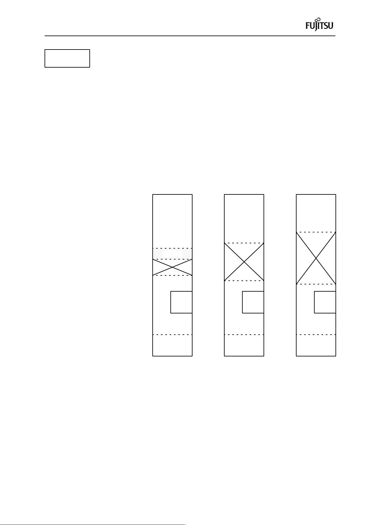
HARDW ARE CONFIGURATION
CPU
Operation Modes
The MB89140 series of microcontrollers is used in the single-chip mode.
The memory map for each mode is as follows:
→
H
→
H
→
H
→
H
→
H
MB89PV140
Internal I/O
RAM
Inhibited
Internal ROM
Address
0000
H
0080
H
0380
H
A000
H
FFFF
H
→
→
→
→
→
MB89146
Internal I/O
RAM
Inhibited
Internal ROM
Address
0000
H
0080
H
0280
H
C000
H
FFFF
H
→
→
→
→
→
MB89145
Internal I/O
RAM
Inhibited
Internal ROM
Address
0000
0080
0480
8000
FFFF
Fig. 2.7 Memory Map in Various Modes
The mode that the device enters depends on the states of the device-mode
pins and the contents of the mode data fetched during the reset sequence.
The relationship between the states and operations of the device-mode pins
is shown below.
MODA Description
0
1
Reset vectors are read from the internal ROM.
Write mode for products containing EPROM.
The mode data should be set as follows:
T2 T1 T0
Mode bits
T2 T1 Operation
0
0
Other than above
T0
0
Select single-chip mode.
Reserved. Do not set.
: Reserved; Specify 0.
2-9
Page 30
HARDW ARE CONFIGURATION
CPU
As shown in the flowchart below, the single-chip mode is set according to the
status of the device mode pins and the mode data fetched during the reset
sequence.
Setting
procedure
Fetch programs from internal ROM.
Mode selected Mode pin Mode data
Single-chip mode(1)→(2) 0 XXXXX000
Power-on
Device mode pin
No
Reset cancel?
Ye s
User ROM
(1) Set 0 at the MODA pin.
(2) All pin ports fetch internal
mode data and reset vectors.
2-10
Page 31

HARDW ARE CONFIGURATION
MAIN/SUBCLOCK
CONTROL BLOCK
Main clock
pulse generator
Subclock
pulse generator
WT1
WT0
2.2 MAIN/SUB CLOCK CONTROL BLOCK
This block controls the standby operation, oscillation stabilization time,
software reset, and clock switching.
Block Diagram
CS0 CS1 SCS STP SLP TMD SPLSCM
Prescaler
1/2
1/4
1/8
1/32
Selector
Selector
Clock
control
CPU operation clock
Resource operation clock
Clock for time-base timer
Clock for watch prescaler
Pin state
Clock
specification
Watch
Sleep
Stop
HC1
From timebase timer
HC2
HC3
Selector
HC4
LC from watch
Ready signal
Hold request signal
Hold acknowledge signal
Stop release signal
Fig. 2.8 Machine Clock Control Block Diagram
Register List
Main/sub clock control block consists of standby control register (STBC)
and system clock control register (SYCC).
8 bit
Address: 0007
Address: 0008
H
H
SYCC
STBC
R/W System clock control register
R/W Standby control register
2-1 1
Page 32

HARDW ARE CONFIGURATION
MAIN/SUBCLOCK
CONTROL BLOCK
Address: 0007
Address: 0008
H
H
SYCC
STBC
Description of Registers
The detail of each register is described below.
(1) Standby-control register (STBC)
Bit 7 Bit 6 Bit 5 Bit 4 Bit 3 Bit 2 Bit 1 Bit 0
Address: 0008
STP SLP SPL RST TMD — — —
H
(W) (W) (R/W) (W) (W)
Initial value
00010XXX
B
[Bit 7] STP: Stop bit
This bit is used to specify switching CPU to the stop mode.
0
1
No operation
Stop mode
This bit is cleared at reset or stop cancellation.
0 is always read when this bit is read.
[Bit 6] SLP: Sleep bit
This bit is used to specify switching the CPU and resources to the sleep
mode.
0
1
No operation
Sleep mode
This bit is cleared at reset, sleep or stop cancellation.
0 is always read when this bit is read.
[Bit 5] SPL: Pin state specifying bit
This bit is used to specify the external pin state in the stop mode.
0
1
Holds state and level immediately before stop mode
High impedance
This bit is cleared at resetting.
[Bit 4] RST: Software reset bit
This bit is used to specify the software reset.
0
1
Generates 16-cycle reset signal
No operation
1 is always read when this bit is read.
Note: If a software reset is performed during operation in a submode, an
oscillation stabilization period is required to switch to the main mode.
Therefore, a reset signal is output during the oscillation stabilization
period.
2-12
Page 33

HARDW ARE CONFIGURATION
MAIN/SUBCLOCK
CONTROL BLOCK
Address: 0007
Address: 0008
H
H
SYCC
STBC
[Bit 3] TMD: Watch bit
This bit is used to specify switching to the watch mode.
0
1
No operation
Watch mode
Writing at this bit is possible only in the submode (SCS = 0). 0 is always read
when this bit is read. This bit is cleared at an interrupt request or reset.
(2) System clock control register (SYCC)
This register controls the clock for operating the CPU and resources.
Bit 7 Bit 6 Bit 5 Bit 4 Bit 3 Bit 2 Bit 1 Bit 0
Address: 0007
SCM — — WT1 WT0 SCS CS1 CS0
H
(R) (R/W) (R/W) (R/W) (R/W) (R/W)
Initial value
X--MM100
B
[Bit 7] SCM: System clock monitor bit
This bit is used to check whether the current system clock is the main clock
or subclock.
Subclock (Main clock is stopping or oscillation of main clock stablizing)
0
Main clock
1
[Bits 4 and Bit 3] WT1 and WT0: Oscillation stabilization time select bits
These bit are used to select the oscillation stabilization wait time of the main
clock.
WT1 WT0 Oscillation stabilization time
1
1
0
0
1
0
1
0
Approximate 218/f
Approximate 217/f
Approximate 214/f
Approximate 24/f
CH
CH
CH
CH
If the main mode is specified by the system clock select bit (SCS), the mode
switches to main mode after the selected wait time has elapsed.
The oscillation stabilization time after resetting is determined by the initial
value.
This bit should not be rewritten during oscillation stabilization or concurrently with switching of the sub-clock to the main clock.
Oscillation stabilization time
with 8 MHz source clock
32.8 ms
16.4 ms
2.0 ms
0ms
f
: Oscillation frequency of main clock
CH
The oscillation stabilization time for the main clock is generated by dividing
the frequency of the main clock. Since the oscillation cycle is unstable immediately after oscillation starts, the above times should be used as the
standard.
2-13
Page 34

HARDW ARE CONFIGURATION
MAIN/SUBCLOCK
CONTROL BLOCK
[Bit 2] SCS: System clock select bit
This bit is used to select the system clock mode.
Selects subclock (32.768 kHz) mode
0
Selects main clock (8 MHz) mode
1
[Bits 1 and 0] CS1 and CS0: System clock select bits (Gear function)
If the main mode is specified by the system clock select bit (SCS), the system clock is as given in the table below.
CS1 CS0 Instruction cycle
0
0
1
1
0
1
0
1
64/f
16/f
8/f
4/f
CH
CH
CH
CH
Instruction execution time
at 8 MHz source clock
8.0 µs
2.0 µs
1.0 µs
0.5 µs
f
: frequency of main clock
CH
2-14
Page 35

HARDW ARE CONFIGURATION
MAIN/SUBCLOCK
CONTROL BLOCK
Clock
mode of
CPU
Main mode
(CS1,
CS0)
(1, 1) SLEEP Oscillates 32.768 kHz
(1, 0) SLEEP Oscillates 32.768 kHz
(0, 1) SLEEP Oscillates 32.768 kHz
Description of Operation
Main/sub clock block has normal and low-power consumption mode. The
low-power consumption mode are described below.
(1) Low-power consumption mode
This chip has three operation modes. The sleep mode, and stop mode in the
table below reduce the power consumption. In the main mode, four system
clocks can be selected according to the system condition to minimize power
consumption.
Table 2-2 Operating State of Low-power Consumption Modes
State
Clock pulse
mode
Main Sub
RUN 4 MHz
Oscillates 4 MHz 4 MHz
STOP Stops Stops Stops External interrupt
RUN 2.0 MHz
Oscillates 4 MHz 2.0 MHz
STOP Stops Stops Stops External interrupt
RUN 1.0 MHz
Oscillates 4 MHz 1.0 MHz
STOP Stops Stops Stops External interrupt
Each operating clock pulse
(3 MHz main clock)
CPU
Stops
Stops
Stops
Time-base
timer
Each
resource
Wake-up source
in each mode
Clock
Various interrupt
requests
Various interrupt
requests
Various interrupt
requests
RUN 250 kHz
Oscillates 4 MHz 250 kHz
(0, 0) SLEEP Oscillates 32.768 kHz
Stops
STOP Stops Stops Stops External interrupt
RUN 32.768 kHz
Oscillates 32.768 kHz 32.768 kHz
Submode — SLEEP Stops Stops
Stops
STOP Stops Stops Stops External interrupt
Watch Stops Oscillates Stops Stops Stops 32.768 kHz Watch external
mode interrupt
Various interrupt
requests
Various interrupt
requests
• The submode stops oscillation of the main clock.
• The SLEEP mode stops only the operating clock pulse of the CPU; other
operations are continued.
• The W ATCH mode stops the functions of all chips other than the special
resources.
• The STOP state stops the oscillation. Data can be held with the lowest
power consumption in this mode.
2-15
Page 36

HARDW ARE CONFIGURATION
MAIN/SUBCLOCK
CONTROL BLOCK
(a) WATCH mode
• Switching to WATCH mode
– Writing 1 at the TMD bit of the STBC register switches the mode to
WATCH mode. Writing is invalid if 1 is set at the SCS bit (bit 2) of the
SYCC register.
– The WA TCH mode stops all chip functions except the watch prescaler ,
external interrupt, and wake-up functions. Therefore, data can be held
with the lowest power consumption.
– The input/output pins and output pins during the WATCH mode can be
controlled by the SPL bit of the STBC register so that they are held in
the state immediately before entering the WA TCH mode or so that they
enter the high-impedance state.
– If an interrupt is requested when 1 is written at the TMD bit , instruction
execution continues without switching to the WATCH mode.
– In the WA TCH mode, the values of registers and RAM immediately be-
fore entering the WATCH mode are held.
• Canceling WATCH mode
– The WATCH mode is canceled by inputting the reset signal and re-
questing an interrupt.
– When the reset signal is input during the WATCH mode, the CPU is
switched to the reset state and the WATCH mode is canceled.
– When an interrupt higher than level 11 is requested from a resource
during the WATCH mode, the WATCH mode is canceled.
– When the I flag and IL bit are enabled like an ordinary interrupt after
canceling, the CPU executes the interrupt processing. When they are
disabled, the CPU executes the interrupt processing from the instruction next to the one before entering the WATCH mode.
– If the WATCH mode is canceled by inputting the reset signal, the CPU
is switched to the oscillation stabilization wait state. Therefore, the reset sequence is not executed unless the oscillation stabilization time is
elapsed. The oscillation stabilization time will be that of the main clock
selected by the WT1 and WT0 bits. However, when Power-on Reset is
not specified by the mask option, the CPU is not switched to the oscillation stabilization wait state, even if the WATCH mode is canceled by
inputting the reset signal.
(b) SLEEP mode
• Switching to Sleep mode
– Writing 1 at the SLP bit (bit 6) of the STBC register switches the mode to
SLEEP mode.
– The SLEEP mode is the mode to stop clock pulse operating the CPU;
only the CPU stops and the resources continue to operate.
– If an interrupt is requested when 1 is written at the SLP bit (bit 6),
instruction execution continues without switching to the SLEEP mode.
– In the SLEEP mode, the values of registers and RAM immediately be-
fore entering the SLEEP mode are held.
2-16
Page 37

HARDW ARE CONFIGURATION
MAIN/SUBCLOCK
CONTROL BLOCK
• Canceling SLEEP mode
– The SLEEP mode is canceled by inputting the reset signal and re-
questing an interrupt.
– When the reset signal is input during the SLEEP mode, the CPU is
switched to the reset state and the SLEEP mode is canceled.
– When an interrupt level higher than 11 is requested from a resource
during the SLEEP mode, the SLEEP mode is canceled.
– When the I flag and IL bit are enabled like an ordinary interrupt after
canceling, the CPU executes the interrupt processing. When they are
disabled, the CPU executes the interrupt processing from the instruction next to the one before entering the SLEEP mode.
(c) STOP mode
• Switching to STOP mode
– Writing 1 at the STP bit (bit 7) of the STBC register switches the mode
to STOP mode.
– The STOP mode varies when the main clock is operating and when the
subclock is operating.
When the main clock is operating: The main clock stops but the sub-
clock does not stop. All chip functions except the watch function stop.
However, no watch interrupt can be accepted.
When subclock is operating: Both the main clock and subclock stop. All
chip functions stop.
– The input/output pins and output pins during the STOP mode can be
controlled by the SPL bit (bit 5) of the STBC register so that they are
held in the mode immediately before entering the STOP mode, or so
that they enter in the high-impedance state.
– If an interrupt is requested when 1 is written at the STP bit (bit 7),
instruction execution continues without switching to the STOP mode.
– In the STOP mode, the values of registers and RAM immediately be-
fore entering the STOP mode are held.
• Canceling STOP mode
– The STOP mode is canceled either by inputting the reset signal or by
requesting an interrupt.
– When the reset signal is input during the STOP mode, the CPU is
switched to the reset state and the STOP mode is canceled.
– When an interrupt higher than level 11 is requested from the external
interrupt circuit during the STOP mode, the STOP mode is canceled.
– When the I flag and IL bit are enabled like an ordinary interrupt after
canceling, the CPU executes the interrupt processing. When they are
disabled, the CPU executes the interrupt processing from the instruction next to the one before entering the STOP mode.
– Four oscillation stabilization times of the main clock can be selected by
the WT1 and WT0 bits. The oscillation stabilization time of the subclock is fixed (at 215/fCH — fCH: frequency of subclock).
2-17
Page 38

HARDW ARE CONFIGURATION
MAIN/SUBCLOCK
CONTROL BLOCK
– If the STOP mode is canceled by inputting the reset signal, the CPU is
switched to the oscillation stabilization wait state. Therefore, the reset
sequence is not executed unless the oscillation stabilization time is
elapsed. The oscillation stabilization time corresponds to the oscillation
stabilization time of the main clock selected by the WT1 and WT0 bits.
However, when Power-on Reset is not specified by the mask option, the
CPU is not switched to the oscillation stabilization wait state even if the
STOP mode is canceled by inputting the reset signal.
(2) Setting low power consumption mode
STBC Register
STP (Bit 7)
0 0 0 Normal
001 WATCH
0 1 0 SLEEP
1 0 0 STOP
1 ×× Disable
Note: When the mode is switched from the subclock mode to the main clock
mode, do not set the Stop, Sleep, and Watch modes. If the SCS bit of
the SYCC register is rewritten from 0 to 1, set the above modes after
the SCM bit of the SYCC register has been set to 1.
SLP (Bit 6) TMD (Bit 3)
Mode
2-18
Page 39

HARDW ARE CONFIGURATION
MAIN/SUBCLOCK
CONTROL BLOCK
Main STOP
Main stop
Sub oscillate
(8)
Oscillation stabilization
waiting of main clock
(1) (2)
(3)
(3) State transition diagram at low power consumption mode
(27)
(7)
(18)
Main SLEEP
Main oscillate
Sub oscillate
(5)
(4)
Main RUN
Main oscillate
Sub oscillate
(17)
Sub RUN
Oscillation stabilization
waiting of main clock
(9)
(6)
(10)
Sub SLEEP
Main stop
Sub oscillate
(28)
(29)
(16)
(15)
Sub RUN
Main stop
Sub oscillate
(11)
(12)
(19)
Oscillation stabilization
waiting of subclock
(20)
(14)
(24)
WATCH
Main stop
Sub oscillate
(25)
Sub STOP
Main stop
Sub stop
(21)
(13)
(26)
(23)
(22)
Power-on
(1) When power-on reset option is selected
(2) When power-on reset option is not selected
(3) After oscillation stabilized
(4) Set STP bit to 1.
(5) Set SLP bit to 1.
(6) Set SCS bit to 0.
(7) External reset when power-on reset option not selected
(8) External reset or interrupt when power-on reset option se-
lected
(9) External reset or interrupt
(10) External reset when power-on reset option not selected
(11) External reset or other reset when power-on reset option
selected
(12) Set SCS bit to 1.
(13) After oscillation stabilized
(14) Set STP bit to 1.
(15) Set TMD bit to 1.
(16) Set SLP bit to 1.
(17) External reset after oscillation stabilized or when power-on
reset option not selected
(18) External reset or other reset when power-on reset option
selected
(19) External reset after oscillation is stabilized or when power-on
reset option not selected
(20) External reset when power-on reset option selected
(21) External reset when power-on reset
option not selected
(22) Interrupt
(23) External reset
when power-on reset
option selected
(24) External reset
when power-on reset
option selected
(25) External reset
when power-on reset
option not selected
(26) Interrupt
(27) External reset
when power-on reset
option selected
(28) External reset
when power-on reset
option not selected
(29) Interrupt
2-19
Page 40

HARDW ARE CONFIGURATION
MAIN/SUBCLOCK
CONTROL BLOCK
Power-on reset
Watchdog timer reset
External reset
Software reset
Reset Control Section
Reset control Internal reset signal
• Reset
There are four types of resets as shown in Table 2-3.
Table 2-3 Sources of Reset
Reset name Description
Power-on reset Turns power on
Watchdog reset Overflows watchdog timer
External-pin reset Sets external-reset pin to Low
Software reset Writes 0 at RST (bit 4) of STBC
When the power-on reset and reset during the stop state are used, the oscillation stabilization time is needed after the oscillator operates. The timebase timer or watch prescaler controls this stabilization time. Consequently ,
the operation does not start immediately even after canceling the reset.
However if Power-on Reset Disabled is selected by the mask option, no oscillation stabilization time is required in any state after external pins have
been released from the reset.
Note: If the Power-on Reset unavailable option is selected, keep the RST
pin Low until the oscillation stabilization time selected in the option
has elapsed after power-on.
2-20
Page 41

HARDW ARE CONFIGURATION
MAIN/SUBCLOCK
CONTROL BLOCK
Single Clock
The single clock can be selected by the mask option. In the single clock operation, the functions are the same as those of the double clock module except that the subclock mode cannot be set. In the single-circuit clock operation, the P71/X1A and P70/X0A function as input ports.
• State transition diagram
Main SLEEP
Main oscillate
(8)
Main STOP
Main stop
(7)
(6)
(5)
(4)
Main RUN
Main oscillate
(3)
Oscillation stabilization
waiting of main clock
(1) (2)
Power-on
(1) When power-on reset
option selected
(2) When power-on reset
option not selected
(3) After oscillation stabilized
(4) Set STP bit to 1.
(5) Set SLP bit to 1.
(6) External reset when power-on reset option not selected
(7) External reset or interrupt when power-on reset option selected
(8) External reset or interrupt
2-21
Page 42

HARDW ARE CONFIGURATION
INTERRUPT
CONTROLLER
Resource #2
•
•
•
Resource #n
F2MC-8L bus
Test
register
G L
G
•
•
•
•
•
•
G
2.3 INTERRUPT CONTROLLER
The interrupt controller for the F2MC-8L family is located between the
2
MC-8L CPU and each resource. This controller receives interrupt re-
F
quests from the resources, assigns priority to them, and transfers the
priority to the CPU; it also decides the priority of same-level interrupts.
Block Diagram
CPU
2
Address decorder
LevelResource #1
L
•
•
•
L
Level
•
•
•
Level
Level
deciding
block
•
•
•
G
•
•
•
Interrupt
vector
generation
block
G
•
•
•
Same level
priority order
deciding
block
G
Fig. 2.9 Interrupt Controller Block Diagram
Register List
Interrupt controller consists of interrupt-level registers (ILR1, 2, and 3).
8 bit
Address: 007C
Address: 007D
Address: 007E
H
H
H
ILR1
ILR2
ILR3
W Interrupt level register #1
W Interrupt level register #2
W Interrupt level register #3
2-22
Page 43

HARDW ARE CONFIGURATION
INTERRUPT
CONTROLLER
Address: 007C
Address: 007D
Address: 007E
[Example]
Interrupt requests
from resources
Description of Registers
The detail of each register is described below.
ILR1
H
ILR2
H
ILR3
H
• Interrupt level register (ILRX: Interrupt Level Register X)
Bit 7 Bit 6 Bit 5 Bit 4 Bit 3 Bit 2 Bit 1 Bit 0
Address: 007C
Address: 007D
Address: 007E
L31 L30 L21 L20 L11 L10 L01 L00
H
L71 L70 L61 L60 L51 L50 L41 L40
H
LB1 LB0 LA1 LA0 L91 L90 L81 L80
H
(W) (W) (W) (W) (W) (W) (W) (W)
Initial value
11111111
B
The ILRX sets the interrupt level of each resource. The digits in the center of
each bit correspond to the interrupt numbers.
MB89140 hardware manual
L3X
Interrupt control module
IR0
IR1
IR2
IR3
IRB
Interrupt
number
#0
#1
#2
#3
#11
Table address
Upper Lower
FFFB
FFFA
FFF9
FFF8
FFF7
FFF6
FFF5
FFF4
FFE5
FFE4
When an interrupt is requested from a resource, the interrupt controller
transfers the interrupt level based on the value set at the 2-bits of the ILRX
corresponding to the interrupt to the CPU. The relationship between the 2
bits of the ILRX and the required interrupt levels is as follows:
Lx1 Lx0 Required interrupt level
0 × 1
10 2
1 1 3 (None)
2-23
Page 44

HARDW ARE CONFIGURATION
INTERRUPT
CONTROLLER
Description of Operation
The functions of interrupt controllers are described below.
• Interrupt functions
The MB89140 series of microcontrollers have 12 inputs for interrupt re-
quests from each resource. The interrupt level is set by 2-bit registers corresponding to each input. When an interrupt is requested from a resource, the
interrupt controller receives it and transfers the contents of the corresponding level register to the CPU. The interrupt to the device is processed as
follows:
(a)An interrupt source is generated inside each resource.
(b) If an interrupt is enabled, an interrupt request is output from each re-
source to the interrupt controller by referring to the interrupt-enable bit
inside each resource.
(c)After receiving this interrupt request, the interrupt controller determines
the priority of simultaneously-requested interrupts and then transfers the
interrupt level for the applicable interrupt to the CPU.
(d)The CPU compares the interrupt level requested from the interrupt con-
troller with the IL bit in the processor status register.
(e)As a result of the comparison, if the priority of the interrupt level is higher
than that of the current interrupt processing level, the contents of the Iflag in the same processor status register are checked.
(f) As a result of the check in step (e), if the I-flag is enabled for an interrupt,
the contents of the IL bit are set to the required level. As soon as the currently-executing instruction is terminated, the CPU performs the interrupt
processing and transfers control to the interrupt-processing routine.
(g) When an interrupt source is cleared by software in the user ’s interrupt
processing routine, the CPU terminates the interrupt processing.
Figure 2.10 outlines the interrupt operation for the MB89140 series of microcontrollers.
Internal bus
PS I IL
Check Comparator
(f)
Level
comparator
(b)
(e) (d)
(c)
Interrupt controller
(g)
MB89140 CPU
Enable FF
Source FF
Register file
AND
(a)
IPLA IR
Resource
Resource
Fig. 2.10 Interrupt-processing Flowchart
2-24
Page 45

HARDW ARE CONFIGURATION
I/O PORTS
P00 to P07*
P10 to P17*
Input
type
CMOS
1
(Hysteresis)
CMOS
1
(Hysteresis)
Output
type
CMOS
push-pull
CMOS
push-pull
2.4 I/O PORTS
The MB89140 series of microcontrollers have eight parallel ports (55
pins, including a buzzer pin). Ports 0, 1 and 3 serve as CMOS I/O ports;
port 2 serves as a CMOS output-only port; ports 4, 5 and 6 serve as Pchannel open-drain high-withstand-voltage ports; port 7 serves as an input-only port. Ports 0 and 1 are also used as analog input ports.
Ports 0, 1, 2 and 3 are also used as resources.
The BZ pin serves as a P-channel open-drain high-withstand-voltage pin
only for buzzer output.
List of port functions
Table 2-4 List of Port Functions
Function
Parallel ports 00 to 07 P07 P06 P05 P04 P03 P02 P01 P00
Resource AN7 AN6 AN5 AN4 AN3 AN2 AN1 AN0
Parallel ports 10 to 17 P17 P16 P15 P14 P13 P12 P11 P10
Resource ADST — — — ANB ANA AN9 AN8
Bit7 Bit6 Bit5 Bit4 Bit3 Bit2 Bit1 Bit0Pin name
P20 to P23 —
P30 to P37
P40 to P47 — Parallel ports 40 to 47 P47 P46 P45 P44 P43 P42 P41 P40
P50 to P57 — Parallel ports 50 to 57 P57 P56 P55 P54 P53 P52 P51 P50
P60 to P67 — Parallel ports 60 to 67 P67 P66 P65 P64 P63 P62 P61 P60
P70 to P71 — Parallel ports 70 and 71 — — ————P71*
CMOS
(Hysteresis)
CMOS
(Hysteresis)
CMOS
push-pull
CMOS
push-pull*
P-channel
open-drain
high-withstand
voltage
P-channel
open-drain
high-withstand
voltage
P-channel
open-drain
high-withstand
voltage
Parallel ports 20 to 23 — — — — P23 P22 P21 P20
Resource — — — — WDG — PWO0 —
Parallel ports 30 to 37 P37 P36 P35 P34 P33 P32 P31 P30
2
Resource DTTI PWO1 EC SI SO SCK INT1
INT0/
TRG
3
P70*
Notes:
*1 To use P07 to P00 and P13 to P10 as input ports, they must be declared for use as general-purpose input
ports at the PCR0 and PCR1 registers after resetting.
*2 P31 serves as an N-channel open-drain pin.
*3 P70 and P71 serve as X0A and X1A pins when the dual-circuit is selected by the mask option.
3
2-25
Page 46

HARDW ARE CONFIGURATION
I/O PORTS
Register list
I/O port consists of the following registers.
Table 2-5 Port register
Register name
Ports 00 to 07 data register (PDR0) R/W 0000
Ports 00 to 07 data direction register(DDR0) W 0001
Ports 10 to 17 data register (PDR1) R/W 0002
Ports 10 to 17 data direction register(DDR1) W 0003
Ports 20 to 27 data register (PDR2) R/W 0004
Reserve 0005
Ports 30 to 37 data register (PDR3) R/W 000C
Ports 30 to 37 data direction register(DDR3) W 000D
Ports 40 to 47 data register (PDR4) R/W 0010
Ports 50 to 57 data register (PDR5) R/W 0011
read/
write
Address
Initial val-
ue
H
H
H
H
H
H
H
H
H
H
XXXXXXXX
00000000
XXXXXXXX
00000000
----0000
XXXXXXXX
00000000
00000000
00000000
B
B
B
B
B
B
B
B
B
Address: 0022
Address: 0023
Ports 60 to 67 data register (PDR6) R/W 0012
Ports 70 to 77 data register (PDR7) R 0013
H
H
00000000
------XX
B
B
Port control register (PCR0, PCR1)
8 bit
Address: 0022
Address: 0023
PCR0
H
PCR1
H
• Port control register (PCR0, PCR1)
Address: 0022
H
H
Bit 7 Bit 6 Bit 5 Bit 4 Bit 3 Bit 2 Bit 1 Bit 0
P07 P06 P05 P04 P03 P02 P01 P00
H
PCR0
PCR1
(W) (W) (W) (W) (W) (W) (W) (W)
Address: 0023
————P13P12P11P10
H
W Port control register 1
W Port control register 2
(W) (W) (W) (W)
Initial value
00000000
Initial value
----0000
B
B
2-26
Page 47

HARDW ARE CONFIGURATION
I/O PORTS
These registers enable P07 to P00 and P13 to P10 to be used as generalpurpose port inputs after resetting. Write 1 at bits corresponding to each pin.
Register value
Status
Used as analog input port. Inhibited for use as general-
0
1
purpose port input. 0 is read when PDR is read.
Used as general-purpose input port (DDR register
must be to 0). Inhibited for use as analog input port.
Description of functions
The function of each port is described below.
(1) P00 to P07: CMOS-type I/O ports (used as analog input)
P10 to P13: CMOS-type I/O ports (used as analog input)
• Switching input and output
These ports have a data-direction register (DDR) and port-data register
(PDR) for each bit. Input and output can be set independently for each
bit. The pin with the DDR set to 1 is set to output, and the pin with the DDR
set to 0 is set to input.
• Operation for output port (DDR = 1)
The value written at the PDR is output to the pin when the DDR is set to 1.
When the PDR is read, usually , the value of the pin is read instead of the
contents of the output latch. However, when the Read Modify Write
instruction is executed, the contents of the output latch are read irrespective of the DDR setting conditions. Therefore, the bit-processing instruction can be used even if input and output are mixed with each other. When
data is written to the PDR, the written data is held in the output latch irrespective of the DDR setting conditions.
• Operation for input port (DDR = 0)
When settings the input, the output impedance goes High. Therefore,
when the PDR is read, the value of the pin is read. When 1 is written at the
PCR0 and PCR1 registers, the values of corresponding pins are read as 0
(see Figure 2.11).
• State when reset
The DDR is initialized to 0 by resetting and the output impedance goes
High at all bits. The PDR is not initialized by resetting. Therefore, set the
PDR value before setting the DDR to output. After resetting, each port is
inhibited for use as an input port, which is fixed to Low (see Figure 2.1 1).
When using as an input port, each port must be declared for use as an
input port by writing 0 at the corresponding bits of the PCR0 and PCR1
registers.
• State in stop modes
With the SPL bit of the standby-control register set to 1, in the stop mode,
the output impedance goes High irrespective of the value of the DDR.
2-27
Page 48

HARDW ARE CONFIGURATION
I/O PORTS
Internal data bus
• Analog input
When using as an analog input, set 0 at the DDR to turn off the output transistor. If the bits of the PCR0 and PCR1 registers corresponding to the
ports to be used as analog inputs are 1, write 0 at these registers to inhibit
use as general-purpose input ports. At this time, 0 is always read even if
the value of each port is read (input ports cannot be read).
PDR
PDR read
PDR read
(when Read Modify Write instruction executed)
Output latch
PDR write
A/D converter
DDR
DDR write
Stop mode (SPL = 1)
Input buffer (hysteresis)
Output buffer
A/D channel select
(sampling only)
Set values of PCR0
and PCR1 registers
(default: 0)
Pin
Fig. 2.11 Ports 00 to 07 and 10 to 13
(2) P14 to P16: CMOS-type I/O ports
• Switching input and output
These ports have a data-direction register (DDR) and port-data register
(PDR) for each bit. Input and output can be set independently for each
bit. The pin with the DDR set to 1 is set to output, and the pin with the DDR
set to 0 is set to input.
• Operation for output port (DDR = 1)
The value written at the PDR is output to the pin when the DDR is set to 1.
When the PDR is read, usually , the value of the pin is read instead of the
contents of the output latch. However, when the Read Modify Write
instruction is executed, the contents of the output latch are read irrespective of the DDR setting conditions. Therefore, the bit-processing instruction can be used even if input and output are mixed with each other. When
data is written to the PDR, the written data is held in the output latch irrespective of the DDR setting conditions.
• Operation for input port (DDR = 0)
When settings the input, the output impedance goes High. Therefore,
when the PDR is read, the value of the pin is read.
• State when reset
The DDR is initialized to 0 by resetting and the output impedance goes
High at all bits. The PDR is not initialized by resetting. Therefore, set the
value of the PDR before setting the DDR to output.
2-28
Page 49

HARDW ARE CONFIGURATION
I/O PORTS
Internal data bus
• State in stop modes
With the SPL bit of the standby-control register set to 1, in the stop mode,
the output impedance goes High irrespective of the value of the DDR.
PDR
PDR read
PDR read
(when Read Modify Write instruction executed)
Output latch
PDR write
DDR
DDR write
Stop mode (SPL = 1)
Fig. 2.12 Ports 14 to 16
(3) P20 to P23: CMOS-type output ports
(used as resource output, excluding P20 and P22)
Input buffer (hysteresis)
Output buffer
Pull-up resistor
(option)
Pin
Internal data bus
PDR
PDR read
PDR write
• Operation for output port
The value written at the PDR is output to the pin. Since the content of the
output latch is always read when the PDR is read, the bit-processing
instruction can be used even if the output level varies with load.
• Resource output operation (P23 and P21)
When using as the resource output, setting is performed by the resource
output enable bit. (See the description of each resource.)
• State when reset
At reset, all pins are set to High impedance. When a vector is fetched, the
output from each port is enabled and all pins start serving as output ports.
At reset, the PRD is initialized to 0 and Low level is output at all pins.
• State in stop modes
With the SPL bit of the standby-control register set to 1, in the stop mode,
the output impedance goes High irrespective of the value of the DDR.
Resource output
Resource
output enabled
Output latch
P20 and P22 excluded
Pin
Stop mode (SPL = 1)
Fig. 2.13 Ports 20 to 23
2-29
Page 50

HARDW ARE CONFIGURATION
I/O PORTS
(4) P70 and P71: CMOS-type input ports
• Input port operation
The PDR can only be read and the value of the pin is always read.
Note: When the dual-circuit clock option is selected, P71 and P70 serve as
X1A and X0A pins.
• State when reset
The PDR cannot be initialized by reset.
Internal data bus
PDR
Option
Pin
PDR read
Oscillation circuit
Fig. 2.14 Ports 70 and 71
(5) P30 and P32 to P35 and P17: CMOS type I/O ports
(also used as resource I/O)
• Switching input and output
This port has a data-direction register (DDR) and a port-data register
(PDR) for each bit. Input and output can be set independently for each bit.
The pin with the DDR set to 1 is set to output, and the pin with the DDR set
to 0 is set to input.
• Operation for output port (DDR = 1)
The value written at the PDR is output to the pin when the DDR is set to 1.
When the PDR is read, usually , the value of the pin is read instead of the
contents of the output latch. However, when the Read Modify Write
instruction is executed, the contents of the output latch are read irrespective of the DDR setting conditions. Therefore, the bit-processing instruction can be used even if input and output are mixed with each other. When
data is written to the PDR, the written data is held in the output latch irrespective of the DDR setting conditions.
• Operation for input port (DDR = 0)
When used as the input port, the output impedance goes High. Therefore, when the PDR is read, the value of the pin is read.
• Resource output operation
When using as the resource output, setting is performed by the resource
output enable bit. (See the description of each resource.) Since the resource output enable bit has priority in switching input and output, even if
the DDR is set to 0, any bit is set as the resource output when output is
enabled at each resource. Even if the output from each resource is enabled, the read value of the port is effective, so the resource output value
can be checked.
2-30
Page 51

HARDW ARE CONFIGURATION
I/O PORTS
Internal data bus
• Resource input operation
The pin value at a port with the resource input function is always input for
the resource input irrespective of the setting of the DDR and resource.
Set the DDR to input when using an external signal for the resource input.
• State when reset
When reset, the DDR is initialized to 0 and the output impedance goes
High at all bits. When reset, the PDR is not initialized. Therefore, set the
value of the PDR before setting the DDR to output.
• State in stop modes
With the SPL bit of the standby-control register set to 1, in the stop mode,
the output impedance goes High irrespective of the value of the DDR.
PDR
PDR read
PDR read
(when Read Modify Write instruction executed)
Output latch
Resource
output
Resource
output
enable
Resource
input
Input buffer
Output buffer
Pull-up resistor
option
(Except for P30)
Pin
PDR write
DDR write
DDR
Stop mode (SPL = 1)
Fig. 2.15 Ports 35 to 32, 30 and 17
(6) P31: N-ch open-drain-type ports (also used as resource input)
• Switching input and output
This port has a data-direction register (DDR) and a port-data register
(PDR) for each bit. Input and output can be set independently for each bit.
The pin with the DDR set to 1 is set to output, and the pin with the DDR set
to 0 is set to input.
• Operation for output port (DDR = 1)
The value written at the PDR is output to the pin when the DDR is set to 1.
When the PDR is read, usually , the value of the pin is read instead of the
contents of the output latch. However, when the Read Modify Write
instruction is executed, the contents of the output latch are read irrespective of the DDR setting conditions. Therefore, the bit-processing instruction can be used even if input and output are mixed with each other. When
data is written to the PDR, the written data is held in the output latch irrespective of the DDR setting conditions.
2-31
Page 52

HARDW ARE CONFIGURATION
I/O PORTS
Internal data bus
PDR
PDR read
• Operation for input port (DDR = 0)
When used as the input port, the output impedance goes High. Therefore, when the PDR is read, the value of the pin is read.
• Resource input operation
This pin is used both as a resource input and as a port. The value of the
pin is always input to the port serving as the resource input (irrespective of
the setting conditions of the PDR and resource). When using an external
signal at the resource, set the DDR to 0.
• State when reset
When reset, the DDR is initialized to 0 and the output impedance goes
High at all bits. When reset, the PDR is not initialized. Therefore, set the
value of the PDR before setting the DDR to output.
• State in stop modes
With the SPL bit of the standby-control register set to 1, in the stop mode,
the output impedance goes High irrespective of the value of the DDR.
Resource
input
Input buffer
PDR read
(when Read Modify Write instruction executed)
Output latch
PDR write
DDR
DDR write
Stop mode (SPL = 1)
Fig. 2.16 Port 31
(8) P40 to P47: P-ch open-drain high-withstand-voltage output ports
P50 to P57: P-ch open-drain high-withstand-voltage output ports
P60 to P67: P-ch open-drain high-withstand-voltage output ports
• Operation for output port
The value written at the PDR is output to the pin. When the PDR is read in
this port, usually , the contents of the output latch is read instead of the value of the pin.
• State when reset
The PDR is initialized to 0 at reset, so the output register is turned off at all
bits.
Pin
2-32
Page 53

HARDW ARE CONFIGURATION
I/O PORTS
Internal data bus
PDR
PDR read
PDR write
Stop mode (SPL = 1)
Fig. 2.17 Ports 40 to 47, 50 to 57 and 60 to 67
• State in watch mode
When the SPL bit of the standby-control register is set to 1, in the stop
mode, the output impedance goes High irrespective of the value of the
PDR.
Pch
Output latch
VFDP
Pin
Pull-down resistor
(Option)
(9) BZ: P-ch open-drain high-withstand-voltage output
• Buzzer output
A waveform at the frequency set by the buzzer register (BUZR) is output
to the pin.
Buzzer circuit
Stop mode (SPL = 1)
• State when reset
When reset, the buzzer register (BUZR) is initialized to 0 and the output
impedance goes High.
• State in Stop mode
With the SPL bit of the standby control register is set to 1, the output impedance goes High irrespective of the BUZR value.
Pch
Pin
Fig. 2.18 BZ
2-33
Page 54

HARDW ARE CONFIGURATION
WATCH
PRESCALER
Subclock (L0)
2.5 WATCH PRESCALER
This prescaler has a 15-bit binary counter
Four interval times and three clock pulses can be selected.
This function cannot be used when the single clock module is selected by
the mask option.
Block Diagram
01234567891011121314
31.25 ms
0.25 s
MPX
0.5 s
1.0 s
Address: 000B
Interrupt request
IRQB
WPCR
H
2
WPCR
WIF WIE — — — WS1 WS0 WCLR
Fig. 2.19 Watch Prescaler Block Diagram
Register list
8 bit
Address: 000B
H
WPCR
R/W Watch prescaler control register
Description of Registers
The detail of watch prescaler is described below.
• Watch prescaler control register (WPCR)
Bit 7 Bit 6 Bit 5 Bit 4 Bit 3 Bit 2 Bit 1 Bit 0
Address: 0017
WIF WIE — — — WS1 WS0 WCLR
H
(R/W) (R/W) (R/W) (R/W) (R/W)
Initial value
2-34
00---000
B
Page 55

HARDW ARE CONFIGURATION
WATCH
PRESCALER
[Bit 7] WIF: Watch interrupt flag
When writing, this bit is used to clear the watch interrupt flag.
0
1
Clears watch interrupt flag
No operation
When reading, this bit indicates that the watch interrupt has occurred.
0
1
Watch interrupt not occurred
Watch interrupt occurred
1 is read when the Read Modify Write instruction is read. If the WIF bit is set
to 1 when the WIE bit is 1, an interrupt request is output. This bit is cleared
upon reset.
[Bit 6] WIE: Watch interrupt enable bit
This bit is used to enable an interrupt by the watch.
0
1
Interrupt by watch disabled
Interrupt by watch enabled
[Bit 1 and 0] WS1, WS0: Interrupt interval time specification bit by watch
These bits are used to specify the interrupt cycles.
WS1 WS0 Interrupt cycle
0
0
1
1
0
1
0
1
210/f
213/f
214/f
215/f
CL
CL
CL
CL
fCL: Subclock oscillation frequency
[Bit 0] WCLR: Bit clearing watch prescaler
This bit is used to clear the watch prescaler.
0
1
Watch prescaler cleared
No operation
1 is always read when this bit is read.
Value at fCL = 32.768 kHz
31.25 ms
0.25 s
0.50 s
1.00 s
2-35
Page 56

HARDW ARE CONFIGURATION
WATCHDOG TIMER
RESET
WTE3 to WTE0
CS
Time-base timer
Watch prescaler
2.6 WATCHDOG TIMER RESET
Either of a signal output from the time-base timer for counting with the
main clock or a signal output from the watch prescaler for counting with
the subclock can be selected as a clock. It is possible to select whether or
not a watchdog time-out detect signal is output (only when power-on reset
available option selected).
Block Diagram
Start
CLR
Selector 2-bit counter RSTReset control
OF
WDOS
WDGF
Fig. 2.20 Watchdog Timer Reset Block Diagram
Watchdog
output control
WDG
Address: 0009
Registers
The watchdog timer reset has watchdog timer control register (WDTE).
8 bit
Address: 0009
H
WDTE
R/W Watchdog timer control register
Description of Register
The detail of the watchdog timer control register (WDTE) is described below.
WDTE
H
• Watchdog timer control register (WDTE)
Bit 7 Bit 6 Bit 5 Bit 4 Bit 3 Bit 2 Bit 1 Bit 0
Address: 0009
CS WDOS WDGF — WTE3 WTE2 WTE1 WTE0
H
(R/W) (R/W) (R/W) (W) (W) (W) (W)
Only for power-on
Initial value
000
-XXXX
B
2-36
Page 57

HARDW ARE CONFIGURATION
WATCHDOG TIMER
RESET
[Bit 7] CS: Clock source switching bit
This bit is used to select a count clock from either the watch prescaler or
time-base timer.
22
0
1
Time-base timer cycle = 1/2
Watch prescaler cycle = 1/214 /f
/f
CH
CL
fCH: Main clock frequency
: Subclock frequency
f
CL
Note: Set this bit as soon as the watchdog timer is started. Do not change
the bit after the timer is started. When using the submode, always
select the watch prescaler. Do not select the watchdog prescaler for
the single-circuit clock.
[Bit 6] WDOS: Watchdog output select bit
Bit 6 is used to select output from the pin when the watchdog timer causes a
time-out. (This function cannot be used when the power-on reset unavailable option is selected, write 0 in this case.)
0
1
Output from RST pin (P23 as general-purpose output pin; reset occurs)
Output from P23/WDG pin (reset does not occur)
Note: This bit is not cleared by the reset conditions. This register is cleared
only by a power-on reset.
[Bit 5] WDGF: Watchdog output set bit
Bit 5 is set to 1 when a time-out of the watchdog timer is detected. In this
case, the WDG signal is output when the WDOE is 1. Clearing this bit stops
output of the WDG signal. (This function cannot be used when the power-on
reset unavailable option is selected, write 0 in this case).
The meaning of each bit to be read is as follows:
0
1
No operation
Time-out detected by watchdog timer (WDG output)
1 is always read when the Read Modify instruction is read.
The meaning of each bit to be written is as follows:
0
1
This bit is cleared.
This bit does not change or affect other bits.
Note: This bit is not cleared by the reset conditions. This register is cleared
only by a power-on reset.
2-37
Page 58

HARDW ARE CONFIGURATION
WATCHDOG TIMER
RESET
[Bits 3 to 0] WTE3 to WTE0: Watchdog timer control bit
These bits are used to control the watchdog timer.
First write only after reset
0101
Other than the above
Second and later write
0101
Other than the above
The watchdog timer can be stopped only by reset. 1111 is read when these
bit are read.
Description of operation
The watchdog timer enables detection of a program malfunction.
(1) Starting watchdog timer
The watchdog timer starts when 0101 is written at the watchdog timer control bits.
Watchdog timer started
No operation
Watchdog timer counter cleared
No operation
(2) Clearing watchdog timer
When 0101 is written at the watchdog timer control bits after start, the watch-
dog timer is cleared. The counter of the watchdog timer is cleared when
changing to the standby mode (STOP, SLEEP, WATCH).
(3) Watchdog timer reset
If the watchdog timer is not cleared within the time given in the table below, a
watchdog timer reset occurs to reset the chip internally.
Clock source
Time-base timer Watch prescaler
Minimum time
Maximum time
Approx. 524.3 ms
Approx. 1049 ms
Main clock: 8 MHz clock
Subclock: 32.768 kHz clock
Approx. 512 ms
Approx. 1024 ms
2-38
Page 59

HARDW ARE CONFIGURATION
WATCHDOG TIMER
RESET
CASE 1
Time-base timer output
(Clock prescaler)
Watchdog reset
CASE 2
Time-base timer output
(Clock prescaler)
Watchdog reset
The relationship between the 2-bit counter of the watchdog timer and the
time-base timer (clock prescaler) is as follows:
524.3 (512) ms
Watchdog clear
01 2Watchdog counter
1049 (1024) ms
Watchdog clear
012Watchdog counter
As shown above, the interval time of the watchdog timer changes as shown
in the above table according to the watchdog reset timing.
(4) Stopping watchdog timer
Once started, the watchdog timer cannot be stopped until a reset occurs.
(5) WDG signal operation
(WDOS bit 1 with power-on reset available option selected)
P23/WDG
Watchdog time-out WDGF bit clear
Notes:
1. The WDOS and WDGF bits are cleared only by a power-on reset. There-
fore, if the power-on reset unavailable option is selected, this WDG output cannot be used.
2. With the power-on reset available option selected and the WDGF bit set
to 1, reset does not occur even if the watchdog timer causes a time-out.
3. If the power-on reset unavailable option is selected, the initial values of
the WDGS and WDGF bits become disabled.
4. Reset occurs with the power-on reset unavailable option selected and
the watchdog timer at time-out. At this time, the reset signal will be output
if the reset output available option is selected.
5. The WDG signal continues to output a High level even when an external
or software reset occurs.
2-39
Page 60

HARDW ARE CONFIGURATION
WATCHDOG TIMER
RESET
Set the WDTE register as follows:
First, set the WDOS bit.
(Set WTE3 to WTE0 to a value other
than 0101. Do not set the CS bit.)
Set the CS bit concurrently with
starting the watchdog timer.
(Write 0101 at WTE3 to WTE0.)
Watchdog time-out?
YES
Clear the WDGF flag.
Set WTE3 to WTE0 to a value other than 0101.
Do not rewrite the CS bit.
Do not perform this
operation at a time-out.
NO
2-40
Page 61

HARDW ARE CONFIGURATION
TIME-BASE TIMER
TBTC*
Submode control signal
2.7 TIME-BASE TIMER
This timer has a 21-bit binary counter and uses a clock pulse with 1/2 os-
cillation of the main clock.
Four interval times can be selected.
This function cannot be used when the main clock is stopped.
The clock source of this timer does not change even with a gear change
(1/2 oscillation frequency).
Block Diagram
0123456789
1/2
21-bit counter
10 11 12 13 14 15 16 17 18 19 20
1/2
TBC0
MPX
TBC1
TBR
TBIE
TBIF
Interrupt request
IRQA
* TBTC is a clock pulse with 1/2 oscillation of the original oscillation.
Fig. 2.21 Time-base Timer Block Diagram
Register list
The time-base timer has time-base timer control register (TBCR).
8 bit
Address: 000A
H
TBCR
R/W Time-base timer control register
2-41
Page 62

HARDW ARE CONFIGURATION
TIME-BASE TIMER
Address: 000A
H
TBCR
Description of Registers
The detail of time-base timer control register (TBCR) is described below.
(1) Time-base timer control register (TBCR)
Bit 7 Bit 6 Bit 5 Bit 4 Bit 3 Bit 2 Bit 1 Bit 0
Address: 000A
TBOF TBIE — — — TBC1 TBC0 TBR
H
(R/W) (R/W) (R/W) (R/W) (W)
Initial value
00---000
B
[Bit 7] TBOF: Interval timer overflow bit
When writing, this bit is used to clear the interval timer overflow flag.
0
1
Interval timer overflow flag cleared
No operation
When reading, this bit indicates that an interval timer overflow has occurred.
0
1
Interval timer overflow not occurred
Interval timer overflow occurred
1 is read when the Read Modify Write instruction is read. If the TBIF bit is set
to 1 when the TBIE bit is 1, an interrupt request is output. This bit is cleared
upon reset.
[Bit 6] TBIE: Interval-timer interrupt enable bit
This bit is used to enable an interrupt by the interval timer.
0
1
Interval interrupt disabled
Interval interrupt enabled
[Bit 2 and 1] TBC1, TBC2: Interval time specification bit
These bits are used to specify interval timer cycle.
TBC1 TBC0 Interval time
0
0
1
1
0
1
0
1
0.26 ms
0.51 ms
1.02 ms
0.524 s
[Bit 0] TBR: Time-base timer clear bit
This bit is used to clear time-base timer.
0
1
Time-base timer cleared
No operation
8 MHz source clock
211/f
CH
212/f
CH
213/f
CH
222/f
CH
fCH: main clock frequency
1 is always read when this bit is read.
2-42
Page 63

HARDW ARE CONFIGURATION
8-Bit PWM TIMER
(TIMER 1)
P/TX — P1 P0 TPE TIR OE TIE
IRQ2
System clock
2.8 8-BIT PWM TIMER (TIMER 1)
This timer can be used as an 8-bit timer or PWM controller with 8-bit reso-
lution.
Four clock pulses can be selected.
Block Diagram
Internal data bus
CMRCNTR
Compare register
Selector
1
/
1
1
/
2
1
/
8
1
/
16
Timer/
PWM
Start
CLK
CLEAR
OVER FLOW
8-bit
counter
8
Comparator
PWM generator
and
output control
8
P21/PWO0
Fig. 2.22 8-bit PWM Timer (Timer 1) Block Diagram
Register list
8-bit PWM timer consists of control registers (CNTR) and compare registers
(COMR).
8 bit
Address: 0016
Address: 0017
H
H
COMR
CNTR
W Compare register
R/W Control register
Output
Output
enable
signal
2-43
Page 64

HARDW ARE CONFIGURATION
8-Bit PWM TIMER
(TIMER 1)
Address: 0016
Address: 0017
H
H
COMR
CNTR
Description of Register
The detail of watch prescaler is described below.
(1) Control register (CNTR)
Bit 7 Bit 6 Bit 5 Bit 4 Bit 3 Bit 2 Bit 1 Bit 0
Address: 0017
P/TX — P1 P0 TPE TIR OE TIE
H
(R/W) (R/W) (R/W) (R/W) (R/W) (R/W) (R/W)
Initial value
0-000000
B
[Bit 7] P/TX: Timer/PWM operation switching bit
The operation is performed as the timer when this bit is set to 0, and as the
PWM controller when bit 7 is set to 1.
0
1
Timer
PWM controller
The timer/PWM operation mode should be switched when the counter operation is stopped (TPE = 0), the interrupt is enabled (TIE =0), and the interrupt request flag is cleared (TIR = 0).
[Bits 5 and 4] P1, P0: Clock select bit
The following four system clock cycles can be selected by P1 and P0.
P1 P0
System clock cycle
of PWM timer
At 8 MHz and
Maximum gear speed
0 0 1 system clock cycle 0.5 µs
0 1 2 system clock cycles 1.0 µs
1 0 8 system clock cycles 4.0 µs
1 1 16 system clock cycles 8.0 µs
(One system clock is 500 ns at 8.0 MHz and maximum gear speed.)
These bits must not be rewritten during counting (TPE = 1).
[Bit 3] TPE: Counter operation enable bit
When Bit 3 is set to 1, the timer or PWM control circuit starts operation.
0
1
Counting stop
Counting start
[Bit 2] TIR: Interrupt request flag bit
When an interrupt source occurs, Bit 2 goes to 1. To clear the generated
interrupt source, write 0 at this bit.
The meaning of each bit to be read is as follows:
0
Counter and CMR values do not agree
1
Counter and CMR values agree
2-44
Page 65

HARDW ARE CONFIGURATION
8-Bit PWM TIMER
(TIMER 1)
1 is always read when the Read Modify Write instruction is read.
The meaning of each bit to be written is as follows:
0
1
This bit is cleared.
This bit does not change or affect other bits.
Note: In the PWM operation mode, neither the read nor write values of this
bit have any meaning.
[Bit 1] OE: Output signal control bit
When Bit 1 is 1, the port serves as the timer/PWM output. In the timer operation mode, a signal that is reversed each time the values of the counter and
compare register agree, is output. In the PWM operation mode, a PWM signal is output.
0
1
General-purpose port pin (P21)
Counter/PWM output pin (PWO0)
When this bit is 1, the port functions as the timer/PWM output pin even after
the DDR of P21 is set to input (bit 2 of DDR2).
[Bit 0] TIE: Interrupt enable bit (timer mode)
When this bit is set to 1, an interrupt occurs when the values of the counter
and compare register agree.
Address: 0016
Address: 0017
0
1
Counter interrupt generation disabled
Counter interrupt generation enabled
In the PWM operation mode, an interrupt does not occur irrespective of the
value of this bit.
COMR
H
(2) Compare register (COMR)
In the timer operation mode, this register is used to set the value to be
CNTR
H
compared with the value of the counter, and to clear the counter when the
values of the counter and this register agree. In the PWM operation mode,
the High pulse width can be specified by the value of this register.
Bit 7 Bit 6 Bit 5 Bit 4 Bit 3 Bit 2 Bit 1 Bit 0
Address: 0016
H
(W) (W) (W) (W) (W) (W) (W) (W)
Initial value
XXXXXXXX-
B
2-45
Page 66

HARDW ARE CONFIGURATION
8-Bit PWM TIMER
(TIMER 1)
Count-clock pulse
TPE
Output
TIR bit setting
Value of COMR
Operation description
(1) Timer operation
Setting the P/TX bit of the CNTR to 1, gives the timer operation mode is per-
formed. When the TPE bit of the CNTR is set to 1, the counter starts incrementing from 00H. When the value of the counter agrees with that of the
COMR, the counter is cleared on the next count clock pulse and starts incrementing. Therefore, the TIR bit is set and the output pin is reversed (when
the TPE bit is 0, the output pin is fixed to Low level) in cycles of the count
clock pulses when 00
than those of the count clock pulses when FF
is written at the COMR, or in cycles 256 times longer
H
is written.
H
If the value of the COMR is rewritten in the timer operation mode, it becomes
effective from the next cycle. When the value of the counter is 00
of the COMR is transferred to the comparator latch.
00
00 00 00 00 01 FF 00
FF00
, the value
H
Fig. 2.23 Timer Operation
If the TIE bit of the CNTR is set to 1, an interrupt occurs when the values of
the counter and COMR agree. During interrupt processing, the TIR bit is
used as the interrupt flag. The TIR bit is set irrespective of the value of the
TIE bit. However, if the values of the counter and the COMR agree, the TIR
bit is set to 1 even after an interrupt is disabled.
Writing 0 at the TIR bit permits clearing of the interrupt source or the TIR bit.
When the Read Modify Write instruction is read, the TIR bit is set so that 1 is
always read to prevent erroneous clearing.
The count clock pulse can be selected from four clock pulses from the prescaler by the clock pulse select bits P0 and P1 of the CNTR.
(2) PWM operation
Setting the P/TX bit of the CNTR to 1, gives the PWM operation mode. The
COMR specifies the duty of the output pulse. Pulses can be output with
1/256 resolution and a duty of 0% to 99.6%. When 0 (00
COMR, the duty of the PWM output pulse is 0%; when 128 (80
the duty is 50%, and when 255 (FF
) is written, the duty is 99.6%.
H
) is written at the
H
) is written,
H
The value of the COMR is transferred to the comparator latch when the value of the counter is 00
. If the value of the COMR is rewritten in the PWM
H
operation mode, it becomes effective from the next cycle.
2-46
Page 67

HARDW ARE CONFIGURATION
8-Bit PWM TIMER
(TIMER 1)
• When COMR 00
Counter value 00H⋅⋅⋅⋅⋅⋅→→→→→→→ ⋅⋅⋅⋅⋅⋅ FFH 00
PWM pulse output
• When COMR 80
Counter value 00
PWM pulse output
• When COMR FF
Counter value
PWM pulse output
H
H
⋅⋅ →⋅⋅⋅ 80H⋅⋅⋅ →⋅⋅⋅ FFH 00H⋅⋅ →⋅⋅⋅ 80
H
H
00H⋅ ⋅ ⋅→→→⋅ ⋅ ⋅ 80H⋅⋅⋅⋅→⋅⋅⋅ FFH 00
H
H
H
Fig. 2.24 PWM Pulse Output
The TIR bit of the CNTR in the PWM operation mode has no meaning. No
interrupt occurs irrespective of TIE bit.
The cycle and frequency of the PWM pulse can be changed by switching the
count clock pulse. The count clock pulse can be selected from four clock
pulses from the prescaler (PWM timer channel 1 output) by the clock pulse
select pits P0 and P1 of the CNTR.
2-47
Page 68

HARDW ARE CONFIGURATION
8/16-BIT TIMER
(TIMER 2 AND TIMER 3)
T2STR T2STP T2CS0 T2CS1 — — T2IE T2IF
Rising edge
Falling edge
Both edges
MPX
4.0 µs
2.9 8/16-BIT TIMER (TIMER 2 AND TIMER 3)
Three internal clock pulses and one external clock pulse can be selected.
External input can be selected from the rising edge, falling edge, or both
edges.
Operable in 8-bit 2-ch mode or 16-bit 1-ch mode
Block Diagram
2
CK
8-bit counter
CLR
Comparator
LOAD
Compare data latch
CD
EQ
Interrupt request
IRQ3
0.8 µs
1.6 µs
3.2 µs
Data register
Data register
LOAD
Compare data latch
Comparator
CLR
8-bit counter
MPX
2
CK
T3STR T3STP T3CS0 T3CS1 — — T3IE T3IF
Fig. 2.25 8/16-bit Timer Block Diagram
Internal data bus
EQ
Interrupt request
IRQ4
2-48
Page 69

HARDW ARE CONFIGURATION
8/16-BIT TIMER
(TIMER 2 AND TIMER 3)
Address: 0018
Address: 0019
Address: 001A
Address: 001B
T3CR
H
T2CR
H
T3DR
H
T2DR
H
Register List
8 bit
Address: 0018
Address: 0019
Address: 001A
Address: 001B
H
H
H
H
T3CR
T2CR
T3DR
T2DR
Description of Register Details
The detail of each register is described below.
(1) Timer 2 control register (T2CR)
Bit 7 Bit 6 Bit 5 Bit 4 Bit 3 Bit 2 Bit 1 Bit 0
Address: 0019
T2IF T2IE — — T2CS1 T2CS0 T2STP T2STR
H
(R/W) (R/W) — — (R/W) (R/W) (R/W) (R/W)
[Bit 7] T2IF: Interrupt request flag bit
(When write)
R/W Timer-3 control register
R/W Timer-2 control register
R/W Timer-3 data register
R/W Timer-2 data register
Initial value
X000XXX0
B
T2CS1 T2CS0
0
0
0
1
0
1
Interrupt request flag clearing
No operation
(When read)
0
1
No interrupt request
Interval interrupt request
[Bit 6] T2IE: Interrupt-enable bit
0
1
Interrupt disabled
Interrupt enabled
[Bit 5]: Reserved; write 0 when writing.
[Bit 4]: Reserved; write 0 when writing.
[Bit 3 and 2] T2CS1, T2CS0: Clock source select bit
Time cycle at 8 MHz and
Maximum gear speed
System clock cycle
Rising edge of external clock pulse
Falling edge of external clock pulse
1
1
Both edges of external clock pulse
0
1
4.00 µs
8 system clock cycle
Note: One system clock cycle is 500 ns at 8 MHz and maximum gear speed.
2-49
Page 70

HARDW ARE CONFIGURATION
8/16-BIT TIMER
(TIMER 2 AND TIMER 3)
Address: 0018
Address: 0019
Address: 001A
Address: 001B
T3CR
H
T2CR
H
T3DR
H
T2DR
H
[Bit 1] T2STP: Timer-stop bit
0
1
Counting continued without clearing counter
Counting suspended
[Bit 0] T2STR: Timer-start bit
0
1
Terminates operation
Clears counter and starts operation
(2) Timer 3 control register (T3CR)
Bit 7 Bit 6 Bit 5 Bit 4 Bit 3 Bit 2 Bit 1 Bit 0
Address: 0018
T3IF T3IE — — T3CS1 T3CS0 T3STP T3STR
H
(R/W) (R/W) (R/W) (R/W) (R/W) (R/W) (R/W) (R/W)
[Bit 7] T3IF: Interrupt request flag bit
(When write)
0
1
Interrupt request flag clearing
No operation
Initial value
X000XXX0
B
(When read)
0
1
No interrupt request
Interval interrupt request
[Bit 6] T31E: Interrupt-enable bit
0
1
Interrupt disabled
Interrupt enabled
[Bit 5]: Reserved; write 0 when writing.
[Bit 4]: Reserved; write 0 when writing.
[Bit 3 and 2]: T3CS1, T3CS0: Clock source select bit
T2CS1 T2CS0
0
0
1
1
0
1
0
1
Time cycle at 8 MHz and
Maximum gear speed
1.0 µs
2.0 µs
4.0 µs
16-bit mode
Note: When bit 2 and 3 use only timer 2, set this bit to except 11.
System clock cycle
2 system clock cycle
4 system clock cycle
8 system clock cycle
—
2-50
Page 71

HARDW ARE CONFIGURATION
8/16-BIT TIMER
(TIMER 2 AND TIMER 3)
Address: 0018
Address: 0019
Address: 001A
Address: 001B
T3CR
H
T2CR
H
T3DR
H
T2DR
H
[bit 1] T3STP: Timer stop bit
0
1
Operation continued without clearing counter
Count operation suspended
[Bit 0] T3STR: Timer start bit
0
1
Operation stopped
Operation started after clearing counter
(3) Timer 1 and 2 data registers (T2DR and T2DR)
Bit 7 Bit 6 Bit 5 Bit 4 Bit 3 Bit 2 Bit 1 Bit 0
Address:
001B
H
Address:
001A
H
(R/W) (R/W) (R/W) (R/W) (R/W) (R/W) (R/W) (R/W)
Initial value
XXXXXXXX
Write data is the set interval times and read data is the counted value.
B
2-51
Page 72

HARDW ARE CONFIGURATION
8/16-BIT TIMER
(TIMER 2 AND TIMER 3)
Counter clear
Set data value
Description of Operation
(1) 8-bit internal clock mode
In the 8-bit internal clock mode, three internal clock inputs can be selected
by setting the clock source select bits (T2CS1 and T2CS0, T3CS1 and
T3CS0) of the timer control registers (T2CR and T3CR). The timer data registers (T2DR and T3DR) serve as interval time setting registers.
To start the timer, set the interval time to the timer data registers, write 1 at
the timer start bits (T2STR and T3STR) of the timer control registers to clear
the counter to 00
, and load the values of the timer data registers into the
H
compare latch. Then, counting starts.
When the values of the counter agree with the set value of the timer data
registers, the interval interrupt request flags (T2IF and T3IF) are set to 1. At
this time, the counter is cleared to 00
, the values of the timer data registers
H
are reloaded into the compare latch, and counting is continued. If the interrupt enable bits (T2IE and T3IE) are set to 1, an interrupt request is output to
the CPU. Assuming the set value of the timer data register is n and the selected clock is φ, the interval time (T) can be calculated as follows.
T = φ × (n + 1) [µs]
Matched Matched Matched
Compare latch
Count value
0000
T2STR
T2IF
H
T2IF = 0 (W) T2IF = 0 (W) T2IF = 0 (W)
Fig. 2.26 Description Diagram for Internal Clock Mode Operation
Operation mode specification
Interval time setting
T2STR = 1, T2IF = 0, T2IE = 1
Timer start
Main program
T2IF = 1
Interrupt processing
T2IF = 0 (W)
Fig. 2.27 Flow Diagram for Timer Setting
2-52
Page 73

HARDW ARE CONFIGURATION
8/16-BIT TIMER
(TIMER 2 AND TIMER 3)
External clock
Counter clear
TSTR = 1
Count value
T2DR
T2IF
Fig. 2.28 External Cock Mode Operation Description Diagram
(2) 8-bit external clock mode
In the 8-bit external clock mode, the eternal clock input can be selected
three various external clock inputs by setting the clock source select bits
(T2CS1 and T2CS0) of the timer 2 control register (T2CR). The externalclock input pin of the timer corresponds to P33/EC.
To start the timer, write 1 at the timer start bit (T2STR) of the T2CR to clear
the counter.
When the value of the counter agrees with that of the timer data register, the
interval interrupt request flag bit (T2IF) is set to 1. At this time, if an interrupt
is enabled (T2IE = 1), an interrupt request is output to the CPU.
00
00Undefined
H
01
02
H
H
FF
H
FE
FF
H
00
H
H
FF
H
T2IF = 0 (W)
01
H
CK
CK’
T2STP
T2STR
T2STR’
Count value
(4) Precautions for use of timer stop bit
If the timer stop bit is used to stop the timer, the input clock pulse is fixed to
HIGH, Therefore, the count value varies depending on the level of the input
clock pulse.
After using the timer stop bit to stop the timer, if 00 is written simultaneously
at the timer stop and start bits, the count value may be incremented by one.
Therefore, when using the timer stop bit to stop the timer, read the count
data and then write 0 at the timer start bit (Figure 2.29)
When input clock is High When input clock is Low
Fig. 2.29 Operation Diagram when Timer Stop Bit is Used
2-53
Page 74

HARDW ARE CONFIGURATION
8/16-BIT TIMER
(TIMER 2 AND TIMER 3)
(3) 16-bit mode
In the 16-bit mode, each bit of the timer control registers is as shown below.
Bit 7 Bit 6 Bit 5 Bit 4 Bit 3 Bit 2 Bit 1 Bit 0
Address: 0019
Address: 0018
T2IF T2IE — — T2CS1 T2CS0 T2STP T2STR
H
T3IF T3IE — — T3CS1 T3CS0 T3STP T3STR
H
No operation No operationSet to 11Set to 00
In the 16-bit mode, write 1 1 at the T3CS1 and T3CS0 bits of the T3CR and
set 0 at the bit 5 and bit4.
When in the 16-bit mode, the timer is controlled by the T2CR. The timer data
registers T3DR and T2DR use the upper and lower bytes, respectively.
The clock source is selected by the T2CS1 and T2CS0 bits of the T2CR. T o
start the timer, write 1 at the T2STR bit of the T2CR to clear the counter.
If the value of the counter agrees with that of the timer data register, the T2IF
bit is set to 1. At this time, an interrupt request is output to the CPU if the T2IE
bit is 1.
Note: To read the value of the counter in the 16-bit mode, always read the
value twice to check that it is valid and then use the data.
T2CS1 T2CS0
0
0
0
1
Timer state
Counting stop
Counting
See the 8-bit operation diagram for 16-bit mode operation.
(4) Starting and temporarily stopping timer
The operation of the timer is described below, using timer 2.
(a) When counting after clearing the counter
When the T2STR bit is 0, write 0 at the T2STP bit and 1 at the T2STR
bit. When the T2STR bit is set from 0 to 1, the counter is cleared and
the timer starts counting.
(b) When temporarily stopping timer to count without clearing counter
To stop counting temporarily , set the T2STP and T2STR bits to 11.
To continue counting without clearing the counter from the temporarily-stopped state, set the T2STP and T2STR bits from 11 to 01.
The state of the timer corresponding to the settings of the T2STP
and T2STR bits and the operation of the timer when started from the
state (T2STP and T2STR bits = 01) are as follows:
Operation of timer when started from left state
(bits 1 and 0 = 01)
Counts after clearing counter
Continues counting
1
1
Counting stop
0
Temporary counting stop
1
Counts after clearing counter
Continues counting without clearing counter
2-54
Page 75

HARDW ARE CONFIGURATION
12-BIT MULTIPUL
GENERATOR
(MPG, TIMER 4)
Address: 0024
Address: 0025
Address: 0026
Address: 0027
H
H
H
H
2.10 12-BIT MULTIPUL GENERATOR (MPG, TIMER 4)
A 12-bit-long up timer is provided with one compare clear register for
Four count clock sources can be selected.
The PWM operation or PPG operation at start by an external or internal
Register list
8 bit
MCNT
INTSTR
CMCLBR (H)
CMCLR (H)
cycle setting and one compare register for output pin control to control
one real-time waveform output pin.
trigger can be selected on a programmable basis. This generator can
also be used as a toggle output timer.
R/W Control register
R/W Interrupt status register
CMCLBR (L)
W Compare clear buffer register
⇓
CMCLR (L)
— Compare clear register
Address: 0028
Address: 0029
H
H
OUTCBR (H)
OUTCBR (L)
W Output buffer register
⇓
OUTCR (H)
OUTCR (L)
— Output compare register
2-55
Page 76

HARDW ARE CONFIGURATION
12-BIT MULTIPUL
GENERATOR
(MPG, TIMER 4)
P36/PWO1
Control register
Q
Block diagram
DTTI input: Rising edge
Falling edge
TSL1 TSL0 CKS1 CKS0 SPOL STRG PCN1 PCN0
Output compare buffer
register
OUTCBR
12
OUTCR
Comparator
R
S
Comparator
CMCLR
CMCLBR
Output compare register
12-bit
counter
RST
Compare
clear register
12
Compare clear
buffer register
MPX
CKS
4-bit
prescaler
F2MC-8L
internal data bus
12
2
RST
12
External trigger (TRG) input: Rising edge
Falling edge
Both edges
Interrupt status register
MPX
ESL1 ESL0 CLIE CLIR CMIE CMIR DTIE DTIR
IRQ5 IRQ6 IRQ7
Fig. 2.30 MPG Block Diagram
2-56
Page 77

HARDW ARE CONFIGURATION
12-BIT MULTIPUL
GENERATOR
(MPG, TIMER 4)
Address: 0024
Address: 0025
Address: 0026
Address: 0027
Address: 0028
Address: 0029
H
H
H
H
H
H
MCNT
INTSTR
CMCLBR
(H)
CMCLR
(H)
OUTCBR
(H)
OUTCR
(H)
CMCLBR
(L)
CMCLR
(L)
OUTCBR
(L)
OUTCR
(L)
Description of registers
(1) Control register (MCNT)
This register is used to select the count clock pulse of the timer and the
PWM/PPG function, and to control setting of the software trigger.
(1) Interrupt level register (ILRX: Interrupt Level Register X)
Bit 7 Bit 6 Bit 5 Bit 4 Bit 3 Bit 2 Bit 1 Bit 0
Address: 0024
TSL1 TSL0 CKS1 CKS0 SPOL STRG PCN1 PCN0
H
(R/W) (R/W) (R/W) (R/W) (R/W) (R/W) (R/W) (R/W)
Initial value
00000000
B
[Bits 7 and 6] TSL1 and TSL0: Operation mode select bits
Bits 7 and 6 are used to select the operation mode. The PPG operation
mode or PWM operation mode can be selected as the operation mode. External and software triggers can be selected in the PPG and PWM operation modes.
The retrigger enable mode or retrigger disable mode can be selected as
the PPG operation mode, whereas the retrigger enable mode only is selected as the PWM operation mode.
TSL1
TSL0 Operation mode
0
0
1
Stop
0
PWM operation mode (retrigger enable)
1
0
Retrigger disable
PPG operation mode
1
1
Retrigger enable
Retrigger enable mode: When the start trigger (software trigger or exter-
nal trigger) is re-input during operation of the
MPG, the counter and prescaler of the MPG are
cleared and operation is restarted.
Retrigger disable mode: Even when the start trigger (software trigger or
external trigger) is re-input during operation of the
MPG, it is ignored and operation is continued.
When the PWM operation mode is selected, the initial output of the MPG
enters the reset state (see the block diagram). When the PPG operation
mode is selected, the initial state of the MPG output is changed to the set
state.
When the stop mode is selected after the operation mode, the counter and
prescaler are cleared to inactivate the MPG output.
The operation mode should be selected during operation stop.
2-57
Page 78

HARDW ARE CONFIGURATION
12-BIT MULTIPUL
GENERATOR
(MPG, TIMER 4)
CKS1 CKS0
0
0
1
1
0
1
0
1
[Bits 5 and 4] CKS1 and CKS0: Count clock pulse select bits
Bits 5 and 4 are used to select the count clock pulse (minimum resolution) in
the PWM or PPG operation mode.
Clock pulse to be selected
(at maximum gear speed)
1 system clock cycle (0.5 µs at 8 MHz)
2 system clock cycles (1.0 µs at 8 MHz)
4 system clock cycles (2.0 µs at 8 MHz)
8 system clock cycle (4.0 µs at 8 MHz)
One system clock cycle is 500 ns at 8 MHz and maximum gear speed.
These bits should be set during operation stop.
[Bit 3] SPOL: Output polarity select bit
Bit 3 is used to select the polarity of the waveform output from the MPG. This
bit should be set during operation stop.
0
1
Outputs MPG output waveform with positive polarity
Reverses MPG output waveform for output
Maximum cycle at maximum
gear speed (4096 clock pulses)
2048.0 µs at 8 MHz (488 Hz)
4096.0 µs at 8 MHz (244 Hz)
8192.0 µs at 8 MHz (122 Hz)
1638.42 µs at 8 MHz (61 Hz)
[Bit 2] STRG: Software trigger bit
When the internal trigger mode is selected, when 1 is set at this bit, the timer
and prescaler are cleared and the timer is started. This bit also provides
start by a software trigger. 0 is always read when this bit is read.
0
1
Ignored
Clears timer and prescaler to start timer
[Bits 1 and 0] PCN1 and PCN0: Port output select/overcurrent detect
function control bits
Bits 1 and 0 are used to control whether or not the MPG pulse output pin is
used as the general-purpose pin and set the effective/ineffective edge of the
DTTI input for overcurrent detection. The operation mode should be set during operation stop.
When the DTTI input is enabled, if an error is detected outside the chip, the
MPG output can be set to an inactive level (initial output) by inputting the
edge. At this time, the timer and prescaler are cleared to the stopped state.
To restart output, 0 must be written at the overcurrent detect interrupt request bit to clear the flag. At this time, the MPG restarts outputting the wave-
00
forms set when the DTTI input was detected from the timer value of
after
H
accepting the effective trigger input.
After the DTTI is input in the effective state (PCN1 = 1), if the operation mode
is selected to clear the DTIR flag of the INSTR register, the MPG output goes
inactive in the selected mode.
2-58
Page 79

12-BIT MULTIPUL
GENERATOR
(MPG, TIMER 4)
HARDW ARE CONFIGURATION
PCN1
MPG output: Reset
Timer and prescaler: Reset
PCN0 Operation mode
(P36/PW01) general-purpose pin state0
0
0
1
1
DTTI input Trigger input
Stop
1
0
MPG pulse output
1
PWM operation
In operation
Flag clear
Trigger waiting
MPG output: Reset
Timer and prescaler: Reset
Fig. 2.31 Transition of DTTI Input
Address: 0024
MCNT
H
(2) Interrupt status register (INTSTR)
This register is used to control the trigger input interrupt, compare match
Address: 0025
H
INTSTR
interrupt, and compare clear interrupt. It also selects the polarity of the external trigger edge.
Address: 0026
Address: 0027
Address: 0028
Address: 0029
H
H
H
H
CMCLBR
(H)
CMCLR
(H)
OUTCBR
(H)
OUTCR
(H)
CMCLBR
(L)
CMCLR
(L)
OUTCBR
(L)
OUTCR
(L)
Address: 0025
[Bits 7 and 6] ESL1 and ESL0: External trigger select bits
Bits 7 and 6 are used to select the effective edge input of the external trig-
ger. Input of the effective edge clears the timer and prescaler and starts
the timer.
DTTI input ineffective
Effective at rising edge of DTTI input
Effective at falling edge of DTTI input
PPG operation
In operation
DTTI input Trigger input
Stop
MPG output: Set
Timer and prescaler: Reset
Bit 7 Bit 6 Bit 5 Bit 4 Bit 3 Bit 2 Bit 1 Bit 0
ESL1 ESL0 CLIE CLIR CMIE CMIR DTIE DTIR
H
(R/W) (R/W) (R/W) (R/W) (R/W) (R/W) (R/W) (R/W)
Flag clear
Trigger waiting
MPG output: Set
Timer and prescaler: Reset
Initial value
00000000
B
ESL1 ESL0 External trigger edge
0
0
1
1
No external trigger
0
When rising edge detected, timer cleared ⇒ timer started
1
When falling edge detected, timer cleared ⇒ timer started
0
When both edges detected, timer cleared ⇒ timer started
1
2-59
Page 80

HARDW ARE CONFIGURATION
12-BIT MULTIPUL
GENERATOR
(MPG, TIMER 4)
[Bit 5] CLIE: Compare clear match interrupt enable bit
Bit 5 is used to enable the compare clear match interrupt request.
0
1
[Bit 4] CLIR: Compare clear match interrupt request flag
Bit 4 is set to 1 when the compare clear match occurs.
Writing 0 clears this bit.
Writing 1 has no meaning.
1 is always read when the Read Modify Write instruction is read.
0
1
[Bit 3] CMIE: Output compare match interrupt enable bit
Bit 3 is used to enable the compare match interrupt.
0
1
Compare clear match interrupt request disabled
Compare clear match interrupt request enabled
Compare clear match interrupt not requested
Compare clear match interrupt requested
Output compare match interrupt request disabled
Output compare match interrupt request enabled
[Bit 2] CMIR: Output compare match interrupt request flag
Bit 2 is set to 1 when the compare match occurs.
Writing 0 clears this bit.
Writing 1 has no meaning.
1 is always read when the Read Modify Write instruction is read.
0
1
[Bit 1] DTIE: Overcurrent detection interrupt enable bit
Bit 1 is used to enable the overcurrent detection interrupt request.
0
1
[Bit 0] DTIR: Overcurrent detection interrupt request flag
Bit 0 is set to 1 when the effective rising/falling edge is input to the DTTI input
pin. This bit is not set when the PCN1 bit of the MCNT register is 0.
Writing 0 clears this bit.
Writing 1 has no meaning.
1 is always read when the Read Modify Write instruction is read.
Output compare match interrupt not requested
Output compare match interrupt requested
Overcurrent detection interrupt request disabled
Overcurrent detection interrupt request enabled
0
1
No effective input to DTTI input pin
Effective input to DTTI input pin
2-60
Page 81

HARDW ARE CONFIGURATION
12-BIT MULTIPUL
GENERATOR
(MPG, TIMER 4)
Address: 0024
Address: 0025
Address: 0026
Address: 0027
Address: 0028
Address: 0029
H
H
H
H
H
H
MCNT
INTSTR
CMCLBR
(H)
CMCLR
(H)
OUTCBR
(H)
OUTCR
(H)
CMCLBR
(L)
CMCLR
(L)
OUTCBR
(L)
OUTCR
(L)
(3) Compare clear register (CMCLR)
This register is used to store the compare value of compare clear.
When the values of this register and timer agree, the timer is cleared. The
value is transferred from the buffer register to the compare register.
Bit 15 Bit 14 Bit 13 Bit 12 Bit 11 Bit 10 Bit 9 Bit 8
————CLRB CLRA CLR9 CLR8
Initial value
----0000
B
Bit 7 Bit 6 Bit 5 Bit 4 Bit 3 Bit 2 Bit 1 Bit 0
CLR7 CLR6 CLR5 CLR4 CLR3 CLR2 CLR1 CLR0
Initial value
00000000
B
In the PPG operation mode, the match between the value of this register + 1
and the value of the timer is detected to clear the timer and set the MPG output.
In the PWM operation mode, the match between the value of this register + 1
and the value of the timer is detected to clear the timer and set the MPG output.
Address: 0024
Address: 0025
Address: 0026
Address: 0027
Address: 0028
Address: 0029
H
H
H
H
H
H
MCNT
INTSTR
CMCLBR
(H)
CMCLR
(H)
OUTCBR
(H)
OUTCR
(H)
CMCLBR
(L)
CMCLR
(L)
OUTCBR
(L)
OUTCR
(L)
(4) Compare clear buffer register (CMCLBR)
This register is used to store the compare value of compare clear.
The value written to the compare clear buffer register when the timer stops
is written directly to the compare clear register.
Data transfer from the compare clear buffer register to the compare clear
register after the timer starts is done when the compare clear match occurs.
Bit 15 Bit 14 Bit 13 Bit 12 Bit 11 Bit 10 Bit 9 Bit 8
Address: 0026
Address: 0027
————CLRB CLRA CLR9 CLR8
H
(W) (W) (W) (W)
Initial value
----0000
Bit 7 Bit 6 Bit 5 Bit 4 Bit 3 Bit 2 Bit 1 Bit 0
CLR7 CLR6 CLR5 CLR4 CLR3 CLR2 CLR1 CLR0
H
(W) (W) (W) (W) (W) (W) (W) (W)
Initial value
00000000
B
B
Note: T o write the value to the output compare register buffer register during
PWM or PPG operation, use the load instruction. Some time should
be taken to allow writing of the load instruction to terminate until the
values of the compare clear register and timer agree.
2-61
Page 82

HARDW ARE CONFIGURATION
12-BIT MULTIPUL
GENERATOR
(MPG, TIMER 4)
Address: 0024
Address: 0025
Address: 0026
Address: 0027
Address: 0028
Address: 0029
H
H
H
H
H
H
MCNT
INTSTR
CMCLBR
(H)
CMCLR
(H)
OUTCBR
(H)
OUTCR
(H)
CMCLBR
(L)
CMCLR
(L)
OUTCBR
(L)
OUTCR
(L)
(5) Output compare register (OUTCR)
This register is used to store the compare value of output compare.
When the values of this register and timer agree, the output is set.
Bit 15 Bit 14 Bit 13 Bit 12 Bit 11 Bit 10 Bit 9 Bit 8
————CPRB CPRA CPR9 CPR8
Initial value
----0000
B
Bit 7 Bit 6 Bit 5 Bit 4 Bit 3 Bit 2 Bit 1 Bit 0
CPR7 CPR6 CPR5 CPR4 CPR3 CPR2 CPR1 CPR0
Initial value
00000000
In the PPG operation mode, the output is cleared by the external trigger or
software trigger input, and reset when the value of this register and the value
of the timer agree.
In the PWM operation mode, the output is reset by the external trigger or
software trigger input, and reset when the value of this register and the value
of the timer agree.
The pulse width can be specified by the value of this register.
B
Address: 0024
Address: 0025
Address: 0026
Address: 0027
Address: 0028
Address: 0029
H
H
H
H
H
H
MCNT
INTSTR
CMCLBR
(H)
CMCLR
(H)
OUTCBR
(H)
OUTCR
(H)
CMCLBR
(L)
CMCLR
(L)
OUTCBR
(L)
OUTCR
(L)
(6) Output compare buffer register (OUTCBR)
This register is used to store the output compare value.
The value written to the output compare buffer register when the timer
stops is written directly to the output compare register.
Data transfer from the output compare buffer register to the output
compare register after the timer is started is done when the output
compare clear match occurs.
Bit 15 Bit 14 Bit 13 Bit 12 Bit 11 Bit 10 Bit 9 Bit 8
Address: 0028
Address: 0029
————CPRB CPRA CPR9 CPR8
H
(W) (W) (W) (W)
Initial value
----0000
Bit 7 Bit 6 Bit 5 Bit 4 Bit 3 Bit 2 Bit 1 Bit 0
CPR7 CPR6 CPR5 CPR4 CPR3 CPR2 CPR1 CPR0
H
(W) (W) (W) (W) (W) (W) (W) (W)
Initial value
00000000
B
B
Note: Use the load instruction to write the value to the output compare
register buffer register during PWM or PPG operation. Some time
should be taken to allow writing of the load instruction to terminate
until the values of the output compare register and timer agree.
2-62
Page 83

HARDW ARE CONFIGURATION
12-BIT MULTIPUL
GENERATOR
(MPG, TIMER 4)
Operation description
(1) PWM operation (counting)
Timer value
Set value to CMCLR + 1
Set value to OUTCR
00
H
MPG output
Output compare match
Compare clear timer match
Fig. 2.32 Outline of PWM Output
As shown in Figure 2.32, the MPG can generate a PWM waveform. The
repeat cycle is set by the value of the compare clear register, and the duty of
the output pulse is set by the value of the output compare register.
(Software or external)
trigger input
Timer value
03FF
H
02FF
H
01FF
H
00FF
H
Compare clear buffer
register (CMCLBR)
Compare clear
register (CMCLR)
Output compare buffer
register (OUTCBR)
Output compare
register (OUTCR)
MPG output
PW00 pin output
(SPOL = 1)
(01FE)
(01FE)
(00FF)
(00FF)
⇑
CMCLR
Match
Transfer
(03FE)
(03FE)
(02FF)
(02FF)
H
H
H
H
⇑
OUTCR
Match
H
H
H
H
⇑
⇑
CMCLR
Match
Transfer
⇑
OUTCR
Match
OUTCR
Match
Fig. 2.33 Description of PWM Output Operation
2-63
Page 84

HARDW ARE CONFIGURATION
12-BIT MULTIPUL
GENERATOR
(MPG, TIMER 4)
Select output polarity (SPOL = 1 or 0).
Write data to compare clear buffer register or output buffer register.
Select effective edge for external trigger input (ESL1, ESL0).
Select trigger source (TSL1, TSL0) % Set/reset MPG output.
Enable output to pin (PCN1, PCN0
Effective trigger
found?
Yes
Clear counter and prescaler.
Set MPG output.
Counter and prescaler started
CMCLR
compare match?
Yes
Set MPG output.
Counter and prescaler cleared
OUTCBR ⇒ OUTCR transfer
CMCLBR ⇒ CMCLR transfer
≠ (0, 0).
No
No
OUTCR
compare match?
Yes
Reset MPG output.
Setup
Timer count-up
No
Interrupt occurs
when enabled.
Interrupt occurs
when enabled.
When the operation mode is set to “Stop” or when the DTTI input is performed with overcurrent detection enabled, the MPG output (pin state) goes
inactive in this mode.
Fig. 2.34 Flowchart of PWM Operation
Setting the TSL1 and TSL0 bit of the CNTR to 0 and 1 gives the PWM operation mode. The cycle of the output pulse is determined by the value set at the
CMCLR, and the count clock pulse selected by the CKS1 and CKS0 bits.
PWM cycle = (value set at CMCLR + 1) × cycle of count clock pulse
The pulse width is determined by the value set at the OUTCR, and the cycle
of the count clock pulse.
PWM pulse width = value set at OUTCR × cycle of count clock pulse
2-64
Page 85

HARDW ARE CONFIGURATION
12-BIT MULTIPUL
GENERATOR
(MPG, TIMER 4)
For example, the relationship between the value set at the OUTCR and the
duty with 7F
set at the CMCLR is given in Table 2-6 (the output polarity is
H
assumed to be positive (SPOL = 0)).
Table 2-6 Relationship between value Set at OUTCR and Duty
Value set at OUTCR Output wave form Duty
(00)
H
(01)
H
(02)
H
(03)
H
(7D)
H
(7E)
H
(7F)
H
(80)H to (3FF)
H
0%
0.78%
1.56%
2.34%
97.6%
98.4%
99.2%
100%
For (value set at OUTCR > value set at CMCLR) and (value set at OUTCR ≠
0 and value set at CMCLR = 0), a waveform with a duty of 100% is output.
For (value set at OUTCR = 0 and value set at CMCLR = 0) and (value set at
OUTCR = 0 and value set at CMCLR ≠ 0), a waveform with a duty of 0% is
output.
Since the OUTCR and CMCLR have a buffer register , the value of the buffer
can be rewritten before one cycle to change the cycle and duty.
The polarity of the output pulse can be changed by setting the SPOL bit. For
the PWM operation flow, see Figure 2.34.
In the initial state, the timer and prescaler are stopped. The MPG output is in
the reset state. Since the CMCLR and CMCLBR, and the OUTCBR and
OUTCR are connected to each other, simultaneous writing is possible.
The PWM output is started by input of the selected trigger. First, the timer
and prescaler are cleared and the MPG output enters the set state. Then,
the counter starts incrementing.
The MPG output is reset if the values of the OUTCR and counter agree, and
is set if the value of the CMCLR +1 and the value of the timer agree.
If the value of the OUTCR agrees with the value of the CMCLR +1, comparison with the value of the CMCLR + 1 proceeds and the MPG output is set.
The effective edge of the external trigger can be selected by setting the
ESL1 and ESL0 bits.
2-65
Page 86

HARDW ARE CONFIGURATION
12-BIT MULTIPUL
GENERATOR
(MPG, TIMER 4)
The DTTI input pin makes the PWM output inactive at hardware in the event
of an external error. With the DTTI input enabled, when an error is detected,
the DTIR flag is set to inactivate the PWM output. The time required for this
operation is 6 to 8 clock cycles.
Since the DTTI input is edge input, the rising or falling edge can be selected.
To restart the PWM output after recovery from an error, the DTIR flag must
be cleared to provide the effective trigger input. In the event of an interrupt at
DTTI input, other interrupt sources may be set. Therefore, to restart, all
MPG interrupt sources should be cleared. The DTTI input block has a noise
filter.
2-66
Page 87

HARDW ARE CONFIGURATION
12-BIT MULTIPUL
GENERATOR
(MPG, TIMER 4)
(2) PPG operation
(Software or external) trigger input
Timer value
Set value to CMCLR + 1
Set value to OUTCR
00
H
MPG output
Output compare match
Compare clear timer match
Fig. 2.35 Outline of MPG Output
As shown in Figure 2.35, the MPG can generate a PPG waveform. The
MPG output is reset after input of the effective trigger and the time set by the
output compare register has elapsed, and is set after the time set by the
compare clear register has elapsed.
Trigger input
Timer value
03FF
H
02FF
H
01FF
H
00FF
H
Compare clear buffer
register (CMCLBR)
Compare clear
register (CMCLR)
Output compare buffer
register (OUTCBR)
Output compare
register (OUTCR)
MPG output
PW00 pin output
(SPOL = 1)
Fig. 2.36 Description of PPG Output Operation
(03FE)
(03FE)
(00FF)
(00FF)
H
H
⇑
OUTCR
Match
(01FF)
(01FF)
CMCLR
Match
H
H
⇑
H
H
⇑
OUTCR
Match
⇑
CMCLR
Match
2-67
Page 88

HARDW ARE CONFIGURATION
12-BIT MULTIPUL
GENERATOR
(MPG, TIMER 4)
Select output polarity (SPOL = 1 or 0).
Write data to compare clear buffer register or output buffer register.
Select effective edge for external trigger input (ESL1, ESL0).
Select trigger source (TSL1, TSL0) % Set/reset MPG output.
Enable output to pin (PCN1, PCN0
Effective trigger
found?
Yes
Clear counter and prescaler.
Set MPG output.
Counter and prescaler started
CMCLR
compare match?
Yes
Set MPG output.
≠ (0, 0).
No
No
OUTCR
compare match?
Yes
Setup
Timer count-up
No
Reset MPG output.
Interrupt occurs
when enabled.
Interrupt occurs
when enabled.
When the operation mode is set to “Stop” or when the DTTI input is performed with overcurrent detection enabled, the MPG output (pin state) goes
inactive in this mode.
Fig. 2.37 Flowchart of PPG Operation
Setting the TSL1 and TSL0 bit of the CNTR to 0 and 1 or 1 and 1 gives the
PPG operation mode. The PPG operation mode has two modes: retrigger
disable and retrigger enable after effective trigger input.
The MPG output is reset after input of the effective trigger and the time set by
the OUTCR has elapsed, and is set after the time set by the value of the
CMCLR +1 has elapsed. In the initial state, the MPG output is in the set
state.
The time from external trigger input to pulse output is as follows:
2-68
Page 89

HARDW ARE CONFIGURATION
12-BIT MULTIPUL
GENERATOR
(MPG, TIMER 4)
Value set at OUTCBR × count clock cycle + 1.5 to 2 system clock cycles
The time from external trigger input to MPG reset is as follows:
(V alue set at CMCLR +1) × count clock cycle + 1.5 to 2 system clock cycles
For CMCLR ≤ OUTCR, the MPG output is in the set state and the pulse is not
output. For (OUTCR ≠ 0, CMCLR = 0), the MPG output is also in the set
state.
When the value of the OUTCR agrees with the value of the CMCLR +1, the
comparison with the value of the CMCLR + 1 proceeds and the MPG output
is set.
The polarity of the output pulse can be changed by setting the SPOL bit. The
set value must not be changed during pulse output. The operation flow for
PPG output is shown in Figure 2.37.
The DTTI input pin is provided to inactivate the PPG output inactive at hardware in the event of an external error. When the DTTI input is set to ef fective,
when an error is detected, the DTIR flag is set to inactivate the PPG output.
The time required for this operation is 6 to 8 clock cycles (one system clock
cycle is 500 ns at 8 MHz and maximum gear speed).
T o restart the PPG output after recovery from an error, the DTIR flag must be
cleared to input the effective trigger . In the event of an interrupt at DTTI input, other interrupt sources may be set. Therefore, to restart, all MPG interrupt sources should be cleared.
Since the DTTI input is edge input, the rising or falling edge can be selected.
The DTTI input block has a noise filter.
2-69
Page 90

HARDW ARE CONFIGURATION
8-BIT SERIAL I/O
P34/SI
P33/SO
D0 to D7
(MSB first)
SI input
synchronous
circuit
2.11 8-BIT SERIAL I/O
8-bit serial data transfer is possible by the clock synchronous method.
LSB first or MSB first can be selected for data transfer.
Four shift-clock modes (three internal and one external) can be selected.
Block Diagram
Internal data bus
(Shift direction)
⇒⇒⇒⇒⇒⇒
Serial data register (SDR)
D7 to D0
(LSB first)
Transfer
direction
SO output
synchronous
circuit
select
Serial mode
register (SMR)
2
SIOF
SIOE
SCKE
SOE
CKS1
CKS0
BDS
SST
D7 to D0
Overflow
P32/SCK
Internal
clock pulse
Output enable
Output enable
3
Fig. 2.38 8-bit Serial I/O Block Diagram
Register list
The 8-bit serial I/O consists of serial mode register (SMR) and serial data
register (SDR).
Control
circuit
Address: 001C
Address: 001D
Shift-clock
pulse select
Clear
Shift-clock counter
8 bit
H
H
SMR
SDR
IRQ8
R/W Serial mode register
R/W Serial data register
2-70
Page 91

HARDW ARE CONFIGURATION
8-BIT SERIAL I/O
Address: 001C
Address: 001D
H
H
SMR
SDR
Description of Registers
The detail of each register is described below.
(1) Serial-mode register (SMR)
The SMR is used to control serial I/O.
Bit 7 Bit 6 Bit 5 Bit 4 Bit 3 Bit 2 Bit 1 Bit 0
Address: 001C
SIOF SIOE SCKE SOE CKS1 CKS0 BDS SST
H
(R/W) (R/W) (R/W) (R/W) (R/W) (R/W) (R/W) (R/W)
Initial value
00000000
[Bit 7] SIOF: Serial I/O interrupt-request flag
This bit is used to indicate the serial I/O transfer state.
The meaning of each bit when reading is as follows:
0
1
Serial data transfer not terminated
Serial data transfer terminated
Note that 1 is always read when the Read Modify Write instruction is read. If
this bit is set when an interrupt is enabled (SIOE = 1), an interrupt request is
output to the CPU.
The meaning of each bit when writing is as follows:
B
0
1
This bit is cleared.
This bit does not change nor affect other bits.
The end-of-transfer decision may be made by either the SST bit (bit 0 of the
SMR) or by this bit.
[Bit 6] SIOE: Serial I/O interrupt-enable bit
This bit is used to enable a serial I/O interrupt request.
0
1
Serial I/O interrupt-output disable
Serial I/O interrupt-output enable
[Bit 5] SCKE: Shift-clock output-enable bit
This bit is used to control the shift-clock I/O pins.
0
1
General-purpose port pin (P32) or SCK input pin
SCK (shift clock) output pin
When using the P32/SCK pin as an external clock, always set the pin to input
(bit 2 of DDR4 = 0).
2-71
Page 92

HARDW ARE CONFIGURATION
8-BIT SERIAL I/O
CKS1 CKS0
0
0
1
1
Note: One system clock cycle is 500 ns at 8 MHz and maximum gear speed.
[Bit 4] SOE: Serial-data output-enable bit
This bit is used to control the output pin for serial I/O.
0
1
General-purpose port pin (P33)
SO (serial data) output pin
When using P34/SI pin as SI pin, always set the DDR to input (bit 0 of DDR4
= 0).
[Bits 3 and 2] CKS1, CKS0: Shift-clock select bits
These bits are used to select the serial shift-clock modes.
Mode
0
1
0
1
Internal shift-clock mode
Internal shift-clock mode
Internal shift-clock mode
External shift-clock mode
Clock cycle at maximum
gear speed
4 system clock cycle
8 system clock cycle
16 system clock cycle
SCK
SCK
Output
Output
Output
Input
[Bit 1] BDS: Transfer direction select bit
At serial data transfer, this bit is used to select whether data transfer is performed from the least significant bit first (LSB first) or from the most significant bit first (MSB first).
Address: 001C
Address: 001D
0
1
LSB first
MSB first
Note that when this bit is rewritten after writing data to the SDR, the data become invalid.
[Bit 0] SST: Serial I/O transfer-start bit
This bit is used to start serial I/O transfer. The bit is automatically cleared to
0 when transfer is terminated.
0
1
Serial I/O transfer stop
Serial I/O transfer start
Before starting transfer, ensure that transfer is stopped (SST = 0).
SMR
H
(2) Serial-data register (SDR)
This 8-bit register is used to hold serial I/O transfer data. Do not write data
SDR
H
to this register during the serial I/O operation.
Bit 7 Bit 6 Bit 5 Bit 4 Bit 3 Bit 2 Bit 1 Bit 0
Address: 001D
H
(R/W) (R/W) (R/W) (R/W) (R/W) (R/W) (R/W) (R/W)
Initial value
XXXXXXXX
B
2-72
Page 93

HARDW ARE CONFIGURATION
8-BIT SERIAL I/O
Shift-clock pulse
Shift-clock pulse
Description of Operation
The operation of 8-bit serial I/O is described below.
(1) Outline
This module consists of the serial-mode register (SMR) and serial-data reg-
ister (SDR). At serial output, data in the SDR is output in bit serial to the serial output pin (SO) in synchronization with the falling edge of a serial shiftclock pulse generated from the internal or external clock. At serial input,
data is input in bit serial from the serial input pin (SI) to the SDR at the rising
edge of a serial shift-clock pulse.
SDR
#6 #5 #4 #3 #2 #1 #0
#7
CK
P S conversion
SDR
#7 #6 #5 #4 #3 #2 #1 #0
0
Shift-clock pulse
SO
SO
Shift-clock pulse
SI
⋅⋅⋅
#0 #1 #2 #5 #6 #7
#0 #1 #2 #5 #6 #7
⋅⋅⋅
Serial output
⋅⋅⋅
⋅⋅⋅
CK
SI
SI
S P conversion
Serial input
(2) Operation modes
The serial I/O has three internal shift-clock modes and one external shift-
clock mode according to the type of shift-clock, which are specified by the
SMR. Mode switching or clock selection should be made with serial I/O
stopped (SST bit (bit 0) of SMR = 0).
• Internal shift-clock mode
Operation is performed by the internal clock. A shift-clock pulse with a duty
of 50% is output from the SCK pin as a synchronous timing output. Data is
transferred bit-by-bit at every clock pulse.
• External shift-clock mode
Data is transferred bit-by-bit at every clock pulse in synchronization with
the external shift-clock pulse input from the SCK pin. The transfer rate can
be performed from DC to 8 clock cycles (1.00 MHz at 8 MHz).
Do not write data to the SMR and SDR during the serial I/O operation in either mode.
2-73
Page 94

HARDW ARE CONFIGURATION
8-BIT SERIAL I/O
SCK
SST
IRQ
SO
[When transfer terminated]
SCK
SST
SIOF
(3) Interrupt functions
This module can output an interrupt request to the CPU. T o output an inter-
rupt request, set the SIOE bit of the SMR to 1 to enable an interrupt and then
set the interrupt flag SIOF bit of the SMR after 8-bit data transfer is terminated.
#0 #1 #2 #5 #6 #7
#3 #4
(4) Shift start/stop timing
Data transfer starts when 1 is written at the SST bit of the SMR, and stops
when 0 is written. When data transfer is terminated, the SST bit is automatically cleared to 0, which stops the operation.
• Internal shift-clock mode (LSB first)
SO
[When transfer suspended]
SCK
SST
SIOF
SO
[When transfer terminated]
SCK
SST
SIOF
SO
[When transfer suspended]
SCK
SST
SIOF
#0 #1 #2 #5 #6 #7
#0 #1 #2 #5
#3 #4
#3 #4
• External shift-clock mode (LSB first)
#0 #1 #2 #5 #6 #7
#3 #4
SO
#0 #1 #2 #5
#3 #4
Note: When data is written at the SDR, the output data changes at the
falling edge of the external-clock pulse.
Fig. 2.39 Shift Start/Stop Timing
2-74
Page 95

HARDW ARE CONFIGURATION
8-BIT SERIAL I/O
SCK
SI
SO
SCK
SI
SO
(5) Input/output shift timing
Data is output from the serial output pin (SO) at the falling edge of the shift-
clock pulse, and is input from the serial input pin (SI) to the SDR at the rising
edge of the shift-clock pulse.
• LSB first (BDS = 0)
#0 #1 #2 #5 #6 #7
SO output
#0 #1 #2 #5 #6 #7#3 #4
SI input
#3 #4
• MSB first (BDS = 1)
#7 #6 #5 #2 #1 #0
SO output
#7 #6 #5 #2 #1 #0#4 #3
DI7 to DI0 indicate input data, and DO7 to DO0 indicate output data.
SI input
#4 #3
Fig. 2.40 Input/Output Shift Timing
2-75
Page 96

HARDW ARE CONFIGURATION
A/D CONVERTER
P13/ANB
P12/ANA
P11/AN9
P10/AN8
P07/AN7
P06/AN6
P05/AN5
P04/AN4
P03/AN3
P02/AN2
P01/AN1
P00/AN0
Channel
selector
P17/ADST
2.12 A/D CONVERTER
16.5 µs conversion time (at 8 MHz and maximum gear speed)
10-bit resolution
RC sequential comparison A/D converter with sample and hold circuit
Analog input can be selected from 12 channels by the program.
End detection by interrupt or software polling
Starting by software, by external pin trigger, or by timer unit can be se-
lected by the program.
Block Diagram
Internal
Selector
Sample and
hold circuit
Comparator
Control Logic
ADDH and ADDL
data bus
AV
AV
CC
SS
D/A
converter
ADC1 and ADC2
IRQB
Fig. 2.41 A/D Converter Block Diagram
Register list
A/D converter consists of A/D control status registers 1 and 2 and ADC data
register (ADCD).
8 bit
Address: 001E
Address: 001F
Address: 0020
Address: 0021
H
H
H
H
ADC1
ADC2
ADDH
ADDL
R/W AD control states register 1
R/W AD control states register 2
R/W AD control data register (H)
R/W AD control data register (L)
2-76
Page 97

HARDW ARE CONFIGURATION
A/D CONVERTER
Description of Register
The detail of each register is described below.
Address: 001E
ADC1
H
(1) ADC1 (A/D Converter control register)
This register is used to control the A/D converter and display its status.
Address: 001F
Address: 0020
Address: 0021
ADC2
H
ADDH
H
ADDL
H
Address: 001E
H
[Bit 7 to Bit 4] ANS3 to ANS0: Analog input channel select bit
These three bits are used to select an analog input channel.
ANS3 ANS2 Channel selected
0
0
0
0
0
ANS1 ANS0
0
0
0
0
1
0
0
1
1
0
0
1
0
1
0
AN0
AN1
AN2
AN3
AN4
Bit 7 Bit 6 Bit 5 Bit 4 Bit 3 Bit 2 Bit 1 Bit 0
ANS3 ANS2 ANS1 ANS0 AD1 ADMV SIFM AD
(R/W) (R/W) (R/W) (R/W) (R/W) (R) (R/W) (R/W)
Initial value
00000000
ANS3 ANS2
1
1
1
1
1
ANS1 ANS0
0
0
0
0
1
Channel selected
0
0
1
1
0
0
1
0
1
0
AN8
AN9
ANA
ANB
—
B
0
0
0
1
1
1
0
1
1
1
0
1
AN5
AN6
AN7
1
1
1
1
1
1
0
1
1
1
0
1
—
—
—
[Bit 3] ADI: Interrupt flag bit
The meaning of each bit to be read in the A/D mode is as follows:
0
1
Conversion not terminated
Conversion terminated
The meaning of each bit to be read in the sense mode is as follows:
0
1
Conditions specified by SIFM bit not met
Conditions specified by SIFM bit met
In both the A/D and sense modes, an interrupt request is output if this bit is
set when the ADIE (bit 4) of the ADC2 is 1.
The meaning of each bit to be written in the A/D and sense modes is as follows:
0
This bit is cleared.
1
This bit is not changed.
2-77
Page 98

HARDW ARE CONFIGURATION
When reading this bit with the Read Modify Write instructions, 1 is always
read.
A/D CONVERTER
[Bit 2] ADMV: Processing progress flag
Bit 2 indicates the progress of conversion or comparison processing.
0
1
Converting and processing not progressing
Converting and processing progressing
[Bit 1] SIFM: Interrupt source setting bit
This bit is used to set the conditions for setting interrupt source conversion in
the sense mode.
0
1
Set interrupt source when input voltage lower than voltage
set by ADCD register.
Set interrupt source when input voltage higher than voltage set by ADCD register.
[Bit 0] AD: A/D conversion start bit
In both the A/D and sense modes, writing 1 at this bit starts A/D conversion
when the EXT bit (bit 1) of the ADC2 is 0. Writing 0 at this bit has no meaning.
0 is always read. The meaning of each bit to be written is as follows:
0
1
No change
A/D conversion start (When EXT bit (bit 1) of ADC2 is 0)
Address: 001E
ADC1
H
(2) A/D converter control register 2 (ADC2)
The ADC2 is used to control the A/D converter and to indicate its operation
Address: 001F
Address: 0020
Address: 0021
ADC2
H
ADDH
H
ADDL
H
status.
Address: 001F
Bit 7 Bit 6 Bit 5 Bit 4 Bit 3 Bit 2 Bit 1 Bit 0
— TIM1 TIM0 ADCK ADIE ADMD EXT TEST
H
(R/W) (R/W) (R/W) (R/W) (R/W) (R/W) (R/W)
[Bits 6 and 5] TIM1, TIM0: Conversion/comparison time select bits
Bits 6 and 5 are used to select the conversion time or comparison time.
TIM1 TIM0
Conversion time at 8 MHz and
maximum gear speed
Comparison time at 8 MHz and
maximum gear speed
0 0 33 system clock cycles (16.5 µs) 18 system clock cycles (9.0 µs)
0 1 48 system clock cycles (24.0 µs) 33 system clock cycles (16.5 µs)
1 0 66 system clock cycles (33.0 µs) 51 system clock cycles (25.5 µs)
1 1 90 system clock cycles (45.0 µs) 75 system clock cycles (37.5 µs)
Initial value
00000001
B
2-78
Page 99

HARDW ARE CONFIGURATION
A/D CONVERTER
[Bit 4] ADCK: External input clock pulse select bit
Bit 4 is used to select the clock pulse for starting by the external input clock
pulse.
0
1
No change
Operation started (when EXT bit (bit 1) of ADC2 is 1)
[Bit 3] ADIE: Interrupt specification bit
This bit is used to specify interrupt enable/disable.
0
1
Interrupt disabled
Interrupt enabled
[Bit 2] ADMD: Function-switching bit
This bit is used to switch the A/D mode and sense mode.
0
1
A/D mode
Sense mode
[Bit 1] EXT: Start type select bit
Bit 1 is used to select the conversion start type.
Address: 001E
Address: 001F
Address: 0020
Address: 0021
0
1
Starts A/D conversion with AD bit (bit 0) of ADC1
Starts A/D conversion at rising edge of clock selected by
ADCK bit (bit 4) of ADC2
[Bit 0] TEST: Test bit
This bit is used only for testing. Always write 1 at this bit. 1 is always read.
ADC1
H
(3) A/D data registers H and L (ADDH and ADDL)
These registers are used to store the results of A/D conversion in A/D mode
ADC2
H
and write the comparison set value in the Sense mode. Two upper bits and
eight lower bits are assigned to the ADDH and ADDL, respectively.
ADDH
H
ADDL
H
Address: 0020
Address: 0021
Bit 7 Bit 6 Bit 5 Bit 4 Bit 3 Bit 2 Bit 1 Bit 0
—————— 9 8
H
(R/W) (R/W)
76543210
H
(R/W) (R/W) (R/W) (R/W) (R/W) (R/W) (R/W) (R/W)
XXXXXXXX
Initial value
000000XX
Initial value
B
B
2-79
Page 100

HARDW ARE CONFIGURATION
A/D CONVERTER
• When A/D mode
In the A/D mode, the result of the A/D conversion is stored as soon as con-
version is terminated. After the completion of conversion, the value of the
register is held until conversion is restarted.
As soon as conversion is started, the value of the register becomes undefined. Therefore, the conversion value must always be read after the end of
conversion before the next conversion is started.
• When Sense mode
In the Sense mode, the set value to be compared is written beforehand to
this register.
The value of the register, once set, is held unchanged even after compari-
son.
Do not write data during conversion in either the A/D or sense modes.
Description of Operation
The operation of the AD converter is described below.
(1) A/D mode
• Start/restart by software
Writing 0 at the ADMD bit (bit 2) of the ADC2 gives the A/D mode. Writing 1
at the AD (bit 0) of the ADC1 starts the A/D conversion.
When 1 is written at the AD bit (bit 0) of the ADC1 during conversion, the
conversion being executed is aborted to restart the next conversion.
• Start/restart by external clock pulse
Writing 1 at the EXT bit (bit 1) of the ADC2 in the A/D mode gives the standby state for starting by an external clock pulse. When the rising edge of the
clock pulse selected by the ADCK bit (bit 4) of the ADC2 is detected, the
conversion is started.
When the clock pulse is given at the rising edge during conversion, the
conversion being executed is aborted to restart the conversion. If the conversion is started or restarted by the external clock pulse with the EXT bit
(bit 1) of the ADC2 set to 1, it cannot be started or restarted by software.
• End
After completion of conversion, the results are stored in the data register
and the ADI bit (bit 3) of the ADC1 is set. At this time, if the ADIE bit (bit 2) of
the ADC2 is 1, an interrupt request occurs.
The results of conversion are held in the data register until the next conversion is started. Therefore, the conversion value should be read after conversion before the next conversion is started. As soon as the conversion is
started, the previous conversion results are lost.
2-80
 Loading...