

Page 1

FUJITSU SEMICONDUCTOR
CONTROLLER MANUAL
MB89950/950A Series
HARDWARE MANUAL
CM25-10146-1E
F2MC-8L
8-BIT MICROCONTROLLER
Page 2

Page 3

F2MC-8L
8-BIT MICROCONTROLLER
MB89950/950A Series
HARDWARE MANUAL
FUJITSU LIMITED
Page 4

Page 5

PREFACE
■ Objectives and Intended Reader
The MB89950/950A series has been developed as a general-purpose version of the F2MC-8L family
consisting of proprietary 8-bit, single-chip microcontrollers. The MB89950/950A series is applicable to a
wide range of applications from consumer products to industrial equipment, including portable devices.
This manual describes the functions and operation of the MB89950/950A series and is aimed at engineers
using the MB89950/950A series of microcontrollers to develop actual products. See the F
Series Programming Manual for details on the MB89950/950A instruction set.
■ Trademarks
F2MC is the abbreviation of FUJITSU Flexible Microcontroller.
Other system and product names in this manual are trademarks of respective companies or organizations.
TM
The symbols
■ Structure of This Manual
This manual contains the following 12 chapters:
CHAPTER 1 "OVERVIEW"
and ® are sometimes omitted in this manual.
2
MC-8L MB89600
This chapter describes the main features and basic specifications of the MB89950/950A series.
CHAPTER 2 "HANDLING DEVICE"
This chapter describes points to note when using the general-purpose single-chip microcontroller.
CHAPTER 3 "CPU"
This chapter describes the functions and operation of the CPU.
CHAPTER 4 "I/O PORTS"
This chapter describes the functions and operation of the I/O ports.
CHAPTER 5 "TIMEBASE TIMER"
This chapter describes the functions and operation of the timebase timer.
CHAPTER 6 "WATCHDOG TIMER"
This chapter describes the functions and operation of the watchdog timer.
CHAPTER 7 "8-BIT PWM TIMER"
This chapter describes the functions and operation of the 8-bit PWM timer.
CHAPTER 8 "PULSE WIDTH COUNT TIMER (PWC)"
This chapter describes the functions and operation of the pulse width count timer (PWC).
CHAPTER 9 "8-BIT SERIAL I/O"
This chapter describes the functions and operation of the 8-bit serial I/O.
CHAPTER 10 "UART"
This chapter describes the functions and operation of the UART.
CHAPTER 11 "EXTERNAL INTERRUPT CIRCUIT (EDGE)"
This chapter describes the functions and operation of the external interrupt circuit.
i
Page 6

CHAPTER 12 "LCD CONTROLLER/DRIVER"
This chapter describes the functions and operation of the LCD controller/driver.
APPENDIX
This appendix includes I/O maps, instruction lists, and other information.
• The contents of this document are subject to change without notice. Customers are advised to consult with
FUJITSU sales representatives before ordering.
• The information and circuit diagrams in this document are presented as examples of semiconductor device
applications, and are not intended to be incorporated in devices for actual use. Also, FUJITSU is unable to assume
responsibility for infringement of any patent rights or other rights of third parties arising from the use of this
information or circuit diagrams.
• The products described in this document are designed, developed and manufactured as contemplated for general
use, including without limitation, ordinary industrial use, general office use, personal use, and household use, but
are not designed, developed and manufactured as contemplated (1) for use accompanying fatal risks or dangers
that, unless extremely high safety is secured, could have a serious effect to the public, and could lead directly to
death, personal injury, severe physical damage or other loss (i.e., nuclear reaction control in nuclear facility,
aircraft flight control, air traffic control, mass transport control, medical life support system, missile launch control
in weapon system), or (2) for use requiring extremely high reliability (i.e., submersible repeater and artificial
satellite).
Please note that Fujitsu will not be liable against you and/or any third party for any claims or damages arising in
connection with above-mentioned uses of the products.
• Any semiconductor devices have an inherent chance of failure. You must protect against injury, damage or loss
from such failures by incorporating safety design measures into your facility and equipment such as redundancy,
fire protection, and prevention of over-current levels and other abnormal operating conditions.
• If any products described in this document represent goods or technologies subject to certain restrictions on export
under the Foreign Exchange and Foreign Trade Law of Japan, the prior authorization by Japanese government will
be required for export of those products from Japan.
©2002 FUJITSU LIMITED Printed in Japan
ii
Page 7
READING THIS MANUAL
■ Notations of the Register Name and Pin Name
Example for description of register name and bit name
●
Notations of a double-purpose pin
●
P22/SCK pin
Some pins can be used by switching their functions using, for example, settings by a program. Each
double-purpose pin is represented by separating the name of each function using "/".
iii
Page 8

■
Documents and Development Tools Required for Development
Items necessary for the development of this product are as follows.
To obtain the necessary documents and development tools, contact a company sales
representative.
Manuals required for development
●
[Check field]
2
MC-8L MB89950/950A series data sheet (provides a table of electrical characteristics and vari-
F
ous examples of this product)
2
MC-8L Programming Manual (manual including instructions for the F2MC-8L family)
F
*
2
MC Family Softune C Compiler Manual (required only if C language is used for develop-
FR/F
ment) (manual describing how to develop and activate programs in the C language)
*
2
FR/F
MC Family Softune Assembler Manual for V3 (manual describing program development
using the assembler language)
*
2
FR/F
MC Family Softune Linkage Kit Manual for V3 (manual describing functions and opera-
tions of the assembler, linker, and library manager
Manuals with the * mark are attached to each product.
Other manuals, such as those for development, are attached to respective products.
Software required for development
[Check field]
Softune V3 Workbench
Softune V3 for personal ICE (required only if the evaluation is performed for the personal-ICE)
Softune V3 for compact ICE (required only if the evaluation is performed for the compact-ICE)
The type of software product is dependent on the OS to be used.
For details, see the F
2
MC Development Tool Catalog or Product Guide.
iv
Page 9
❍
What is needed for evaluation on the one-time PROM microcomputer (if the programming
operation is performed at your side)
[Check field]
Development tools
●
[Check field]
MB89P955
EPROM programmer
(Programmer available for the MBM27C1001)
Package conversion adapter
ROM-64QF2-28DP-8L3
MB89PV950 (piggyback/evaluation device)
Development tool
References
●
Main unit Pod Probe
MB2141A + MB2144-505 MB2144-203
To use a the other development environment, contact respective makers.
2
•"F
MC Development Tool Catalog"
• "Microcomputer Product Guide"
v
Page 10

vi
Page 11

CONTENTS
CHAPTER 1 OVERVIEW ................................................................................................... 1
1.1 MB89950/950A Series Features ........................................................................................................... 2
1.2 MB89950/950A Series Product Range ................................................................................................. 4
1.3 Differences among Products ................................................................................................................ 6
1.4 Block Diagram of MB89950/950A Series ............................................................................................ 7
1.5 Pin Assignment ..................................................................................................................................... 8
1.6 Package Dimensions .......................................................................................................................... 10
1.7 I/O Pins and Pin Functions ................................................................................................................. 12
CHAPTER 2 HANDLING DEVICES ................................................................................ 17
2.1 Notes on Handling Devices ................................................................................................................ 18
CHAPTER 3 CPU ............................................................................................................ 21
3.1 Memory Space .................................................................................................................................... 22
3.1.1 Special Areas ................................................................................................................................. 24
3.1.2 Storing 16-bit Data in Memory ....................................................................................................... 26
3.2 Dedicated Registers ........................................................................................................................... 27
3.2.1 Condition Code Register (CCR) .................................................................................................... 29
3.2.2 Register Bank Pointer (RP) ........................................................................................................... 32
3.3 General-purpose Registers ................................................................................................................. 33
3.4 Interrupts ............................................................................................................................................. 35
3.4.1 Interrupt Level Setting Registers (ILR1, ILR2, ILR3) ..................................................................... 36
3.4.2 Interrupt Processing ....................................................................................................................... 37
3.4.3 Multiple Interrupts .......................................................................................................................... 39
3.4.4 Interrupt Processing Time .............................................................................................................. 40
3.4.5 Stack Operation during Interrupt Processing ................................................................................. 41
3.4.6 Stack Area for Interrupt Processing ............................................................................................... 42
3.5 Resets ................................................................................................................................................. 43
3.5.1 External Reset Pin ......................................................................................................................... 45
3.5.2 Reset Operation ............................................................................................................................. 46
3.5.3 Pin States during Reset ................................................................................................................. 48
3.6 Clocks ................................................................................................................................................. 49
3.6.1 Clock Generator ............................................................................................................................. 51
3.6.2 Clock Controller ............................................................................................................................. 53
3.6.3 Oscillation Stabilization Delay Time ............................................................................................... 55
3.7 Standby Mode (Low-power Consumption) ......................................................................................... 57
3.7.1 Operating States in Standby Mode ................................................................................................ 58
3.7.2 Sleep Mode ................................................................................................................................... 59
3.7.3 Stop Mode ..................................................................................................................................... 60
3.7.4 Standby Control Register (STBC) .................................................................................................. 61
3.7.5 State Transition Diagram ............................................................................................................... 63
3.7.6 Notes on Using Standby Mode ...................................................................................................... 65
3.8 Memory Access Mode ........................................................................................................................ 67
vii
Page 12

CHAPTER 4 I/O PORTS .................................................................................................. 69
4.1 Overview of I/O Ports .......................................................................................................................... 70
4.2 Port 0 ................................................................................................................................................. 72
4.2.1 Port 0 Data Register (PDR0) ......................................................................................................... 74
4.2.2 Operation of Port 0 ........................................................................................................................ 75
4.3 Port 1 ................................................................................................................................................. 77
4.3.1 Port 1 Data Register (PDR1) ......................................................................................................... 79
4.3.2 Operation of Port 1 ........................................................................................................................ 80
4.4 Port 2 ................................................................................................................................................. 82
4.4.1 Port 2 Data Register (PDR2) ......................................................................................................... 84
4.4.2 Operation of Port 2 ........................................................................................................................ 85
4.5 Port 3 ................................................................................................................................................. 86
4.5.1 Port 3 Data Register (PDR3) ......................................................................................................... 89
4.5.2 Operation of Port 3 ........................................................................................................................ 90
4.6 Port 4 .................................................................................................................................................. 92
4.6.1 Port 4 Registers (PDR4, DDR4) .................................................................................................... 94
4.6.2 Operation of Port 4 ....................................................................................................................... 96
4.7 Program Example for I/O Ports ........................................................................................................... 98
CHAPTER 5 TIMEBASE TIMER ..................................................................................... 99
5.1 Overview of Timebase Timer ........................................................................................................... 100
5.2 Block Diagram of Timebase Timer ................................................................................................... 102
5.3 Timebase Timer Control Register (TBTC) ........................................................................................ 104
5.4 Timebase Timer Interrupt ................................................................................................................. 106
5.5 Operation of Timebase Timer ........................................................................................................... 107
5.6 Notes on Using Timebase Timer ...................................................................................................... 109
5.7 Program Example for Timebase Timer ............................................................................................. 110
CHAPTER 6 WATCHDOG TIMER ................................................................................ 111
6.1 Overview of Watchdog Timer ........................................................................................................... 112
6.2 Block Diagram of Watchdog Timer ................................................................................................... 113
6.3 Watchdog Timer Control Register (WDTC) ...................................................................................... 115
6.4 Operation of Watchdog Timer ........................................................................................................... 116
6.5 Notes on Using Watchdog Timer ...................................................................................................... 118
6.6 Program Example for Watchdog Timer ............................................................................................ 119
CHAPTER 7 8-BIT PWM TIMER ................................................................................... 121
7.1 Overview of 8-bit PWM Timer ........................................................................................................... 122
7.2 Block Diagram of 8-bit PWM Timer .................................................................................................. 124
7.3 Structure of 8-bit PWM Timer .......................................................................................................... 126
7.3.1 PWM Control Register (CNTR) .................................................................................................... 128
7.3.2 PWM Compare Register (COMR) ............................................................................................... 130
7.4 8-bit PWM Timer Interrupts ............................................................................................................... 131
7.5 Operation of Interval Timer Function ................................................................................................ 132
7.6 Operation of PWM Timer Function ................................................................................................... 134
7.7 States in Each Mode during 8-bit PWM Timer Operation ................................................................. 135
7.8 Notes on Using 8-bit PWM Timer ..................................................................................................... 137
viii
Page 13

7.9 Program Example for 8-bit PWM Timer ............................................................................................ 138
CHAPTER 8 PULSE WIDTH COUNT TIMER (PWC) ................................................... 141
8.1 Overview of Pulse Width Count Timer .............................................................................................. 142
8.2 Block Diagram of Pulse Width Count Timer ..................................................................................... 144
8.3 Structure of Pulse Width Count Timer .............................................................................................. 146
8.3.1 PWC Pulse Width Control Register 1 (PCR1) ............................................................................. 148
8.3.2 PWC Pulse Width Control Register 2 (PCR2) ............................................................................. 150
8.3.3 PWC Reload Buffer Register (RLBR) .......................................................................................... 152
8.3.4 PWC Noise Filter Control Register (NCCR) ................................................................................ 154
8.4 Pulse Width Count Timer Interrupts .................................................................................................. 155
8.5 Operation of Interval Timer Function ................................................................................................ 156
8.6 Operation of Pulse Width Measurement Function ............................................................................ 159
8.7 Operation of Noise Filter Circuit ........................................................................................................ 162
8.8 States in Each Mode during Pulse Width Count Timer Operation .................................................... 163
8.9 Notes on Using Pulse Width Count Timer ........................................................................................ 164
8.10 Program Example for Timer Function of Pulse Width Count Timer .................................................. 165
CHAPTER 9 8-BIT SERIAL I/O ..................................................................................... 169
9.1 Overview of 8-bit Serial I/O ............................................................................................................... 170
9.2 Block Diagram of 8-bit Serial I/O ...................................................................................................... 171
9.3 Structure of 8-bit Serial I/O ............................................................................................................... 173
9.3.1 Serial Mode Register (SMR) ........................................................................................................ 176
9.3.2 Serial Data Register (SDR) .......................................................................................................... 179
9.4 8-bit Serial I/O Interrupts ................................................................................................................... 180
9.5 Operation of Serial Output ............................................................................................................... 181
9.6 Operation of Serial Input ................................................................................................................... 183
9.7 States in Each Mode during 8-bit Serial I/O Operation ..................................................................... 185
9.8 Notes on Using 8-bit Serial I/O ......................................................................................................... 188
9.9 Connection Example for 8-bit Serial I/O ........................................................................................... 189
9.10 Program Example for 8-bit Serial I/O ................................................................................................ 190
CHAPTER 10 UART ........................................................................................................ 193
10.1 Overview of UART ............................................................................................................................ 194
10.2 Structure of UART ............................................................................................................................ 199
10.3 UART Pins ........................................................................................................................................ 202
10.4 UART Registers ................................................................................................................................ 204
10.4.1 Serial Mode Control Register 1 (SMC1) ...................................................................................... 205
10.4.2 Serial Rate Control Register (SRC) ............................................................................................. 207
10.4.3 Serial Status and Data Register (SSD) ........................................................................................ 209
10.4.4 Serial Input Data Register (SIDR) ................................................................................................ 211
10.4.5 Serial Output Data Register (SODR) ........................................................................................... 212
10.4.6 Serial Mode Control Register 2 (SMC2) ...................................................................................... 213
10.5 UART Interrupts ................................................................................................................................ 215
10.6 Operation of UART ........................................................................................................................... 216
10.7 Operation of Mode 0, 1, 3 ................................................................................................................ 217
10.8 Program Example for UART ............................................................................................................. 220
ix
Page 14

CHAPTER 11 EXTERNAL INTERRUPT CIRCUIT (EDGE) ............................................ 223
11.1 Overview of the External Interrupt Circuit ........................................................................................ 224
11.2 Block Diagram of the External Interrupt Circuit ................................................................................. 225
11.3 Structure of the External Interrupt Circuit ......................................................................................... 226
11.3.1 External Interrupt Control Register (EIC) ..................................................................................... 228
11.4 External Interrupt Circuit Interrupts ................................................................................................... 230
11.5 Operation of the External Interrupt Circuit ........................................................................................ 231
11.6 Program Example for the External Interrupt Circuit .......................................................................... 232
CHAPTER 12 LCD CONTROLLER/DRIVER .................................................................. 233
12.1 Overview of LCD Controller/Driver .................................................................................................. 234
12.2 Block Diagram of LCD Controller/Driver .......................................................................................... 235
12.2.1 LCD Controller/Driver Internal Voltage Divider ............................................................................ 237
12.2.2 LCD Controller/Driver External Voltage Divider ........................................................................... 239
12.3 Structure of LCD Controller/Driver .................................................................................................... 241
12.3.1 LCD Control Register (LCDR) ..................................................................................................... 244
12.3.2 Segment Output Select Register (SEGR) .................................................................................... 246
12.3.3 Display RAM ................................................................................................................................ 248
12.4 Operation of LCD Controller/Driver .................................................................................................. 250
12.4.1 Output Waveforms during LCD Controller/Driver Operation (1/2 Duty Ratio) ............................. 251
12.4.2 Output Waveforms during LCD Controller/Driver Operation (1/3 Duty Ratio) ............................. 254
12.4.3 Output Waveforms during LCD Controller/Driver Operation (1/4 Duty Ratio) ............................. 257
12.5 Program Example for LCD Controller/Driver .................................................................................... 260
APPENDIX ......................................................................................................................... 263
APPENDIX A I/O Map ................................................................................................................................ 264
APPENDIX B Overview of Instructions ....................................................................................................... 266
B.1 Overview of F
B.2 Addressing ..................................................................................................................................... 269
B.3 Special Instructions ........................................................................................................................ 274
B.4 Bit Manipulation Instructions (SETB, CLRB) .................................................................................. 278
B.5 F
B.6 Instruction map ............................................................................................................................... 286
APPENDIX C Mask Options ....................................................................................................................... 287
APPENDIX D Programming Specifications for One-Time PROM And EPROM Microcontroller ................ 289
D.1 Programming Specifications for One-time PROM and EPROM Microcontrollers .......................... 290
D.2 Programming Yield and Erasure .................................................................................................... 293
D.3 Programming to the EPROM with Piggyback/Evaluation Device ................................................... 294
APPENDIX E MB89950/950A Series Pin States ........................................................................................ 295
2
MC-8L Instructions ..................................................................................................................... 279
2
MC-8L Instructions ................................................................................................. 267
INDEX................................................................................................................................... 297
x
Page 15

CHAPTER 1
OVERVIEW
This chapter describes the main features and basic
specifications of the MB89950/950A series.
1.1 "MB89950/950A Series Features"
1.2 "MB89950/950A Series Product Range"
1.3 "Differences among Products"
1.4 "Block Diagram of MB89950/950A Series"
1.5 "Pin Assignment"
1.6 "Package Dimensions"
1.7 "I/O Pins and Pin Functions"
1
Page 16

CHAPTER 1 OVERVIEW
1.1 MB89950/950A Series Features
The MB89950/950A series is a line of the general-purpose, single-chip microcontrollers.
In addition to a compact instruction set, the microcontrollers contain a variety of
peripheral functions such as an LCD controller/driver, UART, a serial I/O, PWC timer,
PWM timer and external interrupts.
■ MB89950/950A series features
Various package options
●
• QFP packages (0.65 mm lead pitch) for MB89951A/MB89953A/MB89P955 only
High speed processing at low voltage
●
Minimum execution time: 0.8 µs/5 MHz
F2MC-8L family CPU core
●
Instruction set optimized for controllers
• Multiplication and division instructions
• 16-bit arithmetic operations
• Test and branch instructions
• Bit manipulation instructions, etc.
Single-clock control system
●
• Main clock: max. 5 MHz
Four types of timer
●
• 21-bit timebase timer
• Watchdog timer
• 8-bit PWM timer (also can be used as an interval timer)
• 8-bit PWC timer
Two types of serial interface
●
• UART
- 5, 7, 8 bits transfer data length
• Serial I/O
LCD controller/driver
●
• 42 segments x 4 commons (max. 168 pixels)
• Built-in LCD voltage divider
2
Page 17

External interrupts (2 channels)
●
• Two channels are independent and capable of wake-up from low-power consumption mode (with an
edge detection function).
Standby mode (low-power mode)
●
• Stop mode (oscillation stops so as to minimize the current consumption).
• Sleep mode (CPU stops so as to reduce the current consumption to approx. 1/3 of normal).
I/O ports: max. 33 channels
●
• General-purpose I/O ports (N-ch open-drain): 22 (Also serve as segment pins)
• General-purpose I/O ports (N-ch open-drain): 4 (2 also serve as LCD bias pins)
• General-purpose I/O ports (CMOS): 7 (6 also serve as peripheral pins)
CHAPTER 1 OVERVIEW
3
Page 18
CHAPTER 1 OVERVIEW
1.2 MB89950/950A Series Product Range
The MB89950/950A series contains 4 different models. Table 1.2-1 "MB89950/950A
series product line-up" lists the product range and Table 1.2-2 "Common specifications
for the MB89950/950A series" lists the common specifications.
■ MB89950/950A series product range
Table 1.2-1 MB89950/950A series product line-up
Part number
MB89951A MB89953A MB89P955
Classification Mask ROM OTP Piggy-back
ROM size 4K x 8 bits
(internal mask ROM)
RAM size 128 x 8 bits 256 x 8 bits 512 x 8 bits 1024 x 8 bits
Low-power consumption
(Standby mode)
Process CMOS
Operating voltage
*1: Varies with conditions such as operating frequencies.
*2: Use MBM27C256A as the external ROM
*1
2.7 V to 5.5 V 2.7 V to 6.0 V
8K x 8 bits
(internal mask ROM)
Sleep mode and stop mode
16K x 8 bits
(internal OTP)
MB89PV950
32K x 8 bits
(external ROM)
*2
4
Page 19
Table 1.2-2 Common specifications for the MB89950/950A series
Parameter Specification
CPU functions Number of instructions: 136
Instruction bit length: 8 bits
Instruction length: 1 to 3 bytes
Data bit length: 1, 8, 16 bits
Minimum execution time: 0.80 µs to 12.8 µs at 5 MHz
Interrupt processing time: 7.26 µs to 115.2 µs at 5 MHz
CHAPTER 1 OVERVIEW
Peripheral
functions
Ports
20-bit timebase
timer
Watchdog timer Reset generate cycle: min. 419.4 ms at 5 MHz
8-bit PWM
timer
PWC timer 8-bit interval timer operation
UART Transfer data length: 5, 7, 8 bits
8-bit serial I/O 8 bits
General-purpose I/O ports (N-ch open-drain): 22 (also serve as LCD segment pins)
General-purpose I/O ports (N-ch open-drain): 4 (two also serve as LCD bias pins)
General-purpose I/O ports (CMOS): 7 (6 ports serve as peripherals)
Total: 33 (max.)
20 bits
Interrupt cycle: 6.55 ms, 26.21 ms, 104.86 ms, 419.43 ms at 5 MHz
8-bit reload timer operation (square wave output; operating frequency: 0.8 µs, 12.8 µs,
51.2 µs at 5 MHz)
8-bit resolution PWM operation (conversion frequency: 204.8 µs - 3.36 s)
Event count function
8-bit pulse width measurement (continuous measurement, High-width, Low-width measurement and
One-cycle measurement)
Operation clock (0.8 µs, 3.2 µs, 25.6 µs at 5 MHz)
Internal baud rate generator (Max. 78125 bps at 5 MHz)
LSB first/MSB first selectability
One clock selectable from four transfer clocks (one external shift clock, three internal shift clocks: 1.6
µs, 6.4 µs, 25.6 µs at 5 MHz)
*1
LCD controller/
driver
External
interrupt
Note:
Unless otherwise specified, values given for clock cycle, conversion times, etc. are for 5 MHz operation.
*1: Segment pins can be selected by mask option.
Common output: 4 (max.)
Segment output: 42 (max.)
Operation mode: 1/2 bias and 1/2 duty, 1/3 bias and 1/3 duty, 1/3 bias and 1/4 duty
LCD display RAM size: 21 bytes (42 x 4 bits, max. 168 pixels)
Dividing voltage for LCD driving: built-in/external voltage divider selectable
2 independent channels (interrupt vector, request flag, request output enable)
Edge selectability (rising/falling)
5
Page 20

CHAPTER 1 OVERVIEW
1.3 Differences among Products
This section describes the differences among the 4 products in the MB89950/950A
series and lists points to note in product selection.
■ Differences among products and points to note for product selection
Table 1.3-1 Package and corresponding products
Package Part number
MB89951A MB89953A MB89P955 MB89PV950
FPT-64P-M09
(LQFP-64, 0.65 mm pitch)
MQP-64C-P01
(MQFP-64, 1 mm pitch)
: Available
X: Not available
Current consumption
●
• In the case of the MB89PV950, add the current consumed by the EPROM, which is connected to the top
socket.
• When operated at low speed, the product with a one-time PROM (OTPROM) or an EPROM will
consume more current than the product with mask ROM. However the current consumption in sleep/
stop mode, is the same.
For more information about the package, see Section 1.6 "Package Dimensions".
• For more information about the current consumption, see the electrical characteristics in the Data Sheet.
Mask options
●
X
XXX
Functions that can be selected as options and how to designate these options vary from product to product.
Before using, check Appendix C, "Mask Options".
Take particular care on the following points:
• In the MB89951A and MB89953A, the number of common and segment outputs is specified by Data
Release Form.
• Options are fixed on the MB89PV950. (See Appendix C, "Mask Options")
6
Page 21
CHAPTER 1 OVERVIEW
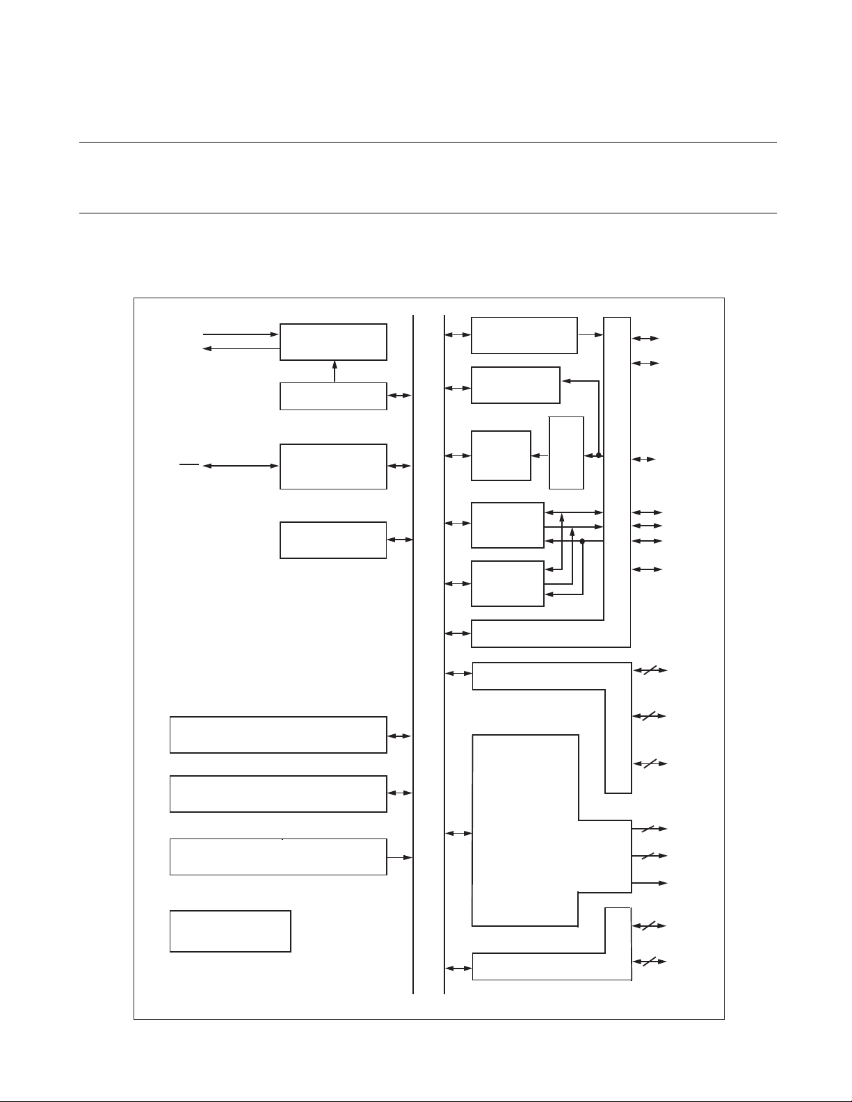
1.4 Block Diagram of MB89950/950A Series
Figure 1.4-1 "MB89950/950A series overall block diagram" shows the block diagram of
the MB89950/950A series.
■ MB89950/950A series block diagram
Figure 1.4-1 MB89950/950A series overall block diagram
X0
X1
RST
Other pins
MODA
V
, VSS
CC
Clock control circuit
(Watchdog timer)
Timebase timer
R A M
2
MC-8L
F
CPU
R O M
Main oscillator
circuit
Reset circuit
Internal bus
8-bit PWM timer
External interrupt
8-bit
pulse width
count timer
8-bit serial I/O
UART
CMOS I/O port
N-ch open-drain I/O port
LCD controller/driver
N-ch open-drain I/O port
Noise
filter
Port 4
Port 0/1/2
Port 3
P41/PWM
P40
P42/PWC/
INT1
P45/SCK
P44/SO
P43/SI
P46/INT0
8
P00/SEG20 to
P07/SEG27
8
P10/SEG28 to
P17/SEG35
6
P20/SEG36 to
P25/SEG41
20
SEG0 to
SEG19
4
COM0 to
COM3
V3
P33/V2
2
P32/V1
2
P30, P31
7
Page 22
CHAPTER 1 OVERVIEW
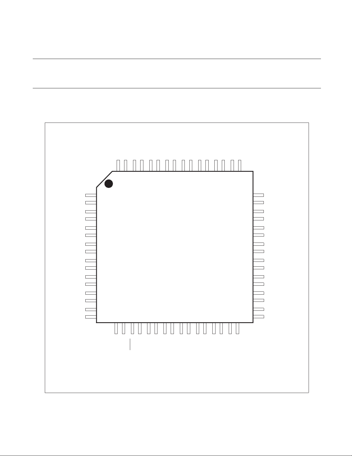
1.5 Pin Assignment
Figure 1.5-1 "FPT-64P-M09 pin assignment" and Figure 1.5-2 "MQP-64C-P01 pin
assignment" show the pin assignment diagrams for the MB89950/950A series.
■ FPT-64P-M09 pin assignment
Figure 1.5-1 FPT-64P-M09 pin assignment
SEG5
SEG6
SEG7
SEG8
SEG9
SEG10
SEG11
SEG12
VCCSEG13
SEG14
SEG15
SEG16
SEG17
SEG18
SEG19
SEG4
SEG3
SEG2
SEG1
SEG0
COM3
COM2
COM1
COM0
V3
P33/V2
P32/V1
P31
P30
P40
P41/PWM
1
2
3
4
5
6
7
8
9
10
11
12
13
14
15
16
646362616059585756555453525150
TOP VIEW
QFP-64
171819202122232425262728293031
X1
SS
V
P45/SCK
P46/INT0
P25/SEG41
P24/SEG40
P23/SEG39
P22/SEG38
P21/SEG37
MODA
P44/SO
X0
RST
P43/SI
P42/INT1/PWC
32
P20/SEG36
49
48
47
46
45
44
43
42
41
40
39
38
37
36
35
34
33
P00/SEG20
P01/SEG21
P02/SEG22
P03/SEG23
P04/SEG24
P05/SEG25
P06/SEG26
P07/SEG27
P10/SEG28
P11/SEG29
P12/SEG30
P13/SEG31
P14/SEG32
P15/SEG33
P16/SEG34
P17/SEG35
8
Page 23
■ MQP-64C-P01 pin assignment
Figure 1.5-2 MQP-64C-P01 pin assignment
SEG6
SEG7
SEG8
SEG9
SEG10
SEG11
SEG12
Vcc
SEG13
SEG14
SEG15
SEG16
64636261605958575655545352
CHAPTER 1 OVERVIEW
SEG17
SEG5
SEG4
SEG3
SEG2
SEG1
SEG0
COM3
COM2
COM1
COM0
V3
V2/P33
V1/P32
P31
P30
P40
P41/PWM
P42/PWC/INT1
P43/SI
1
2
3
4
5
6
7
8
9
10
11
12
13
14
15
16
17
18
19
84838281807978
85
86
87
88
89
90
91
92
93
94959665666768
(TOP VIEW)
20212223242526272829303132
X0
X1
RST
P44/SO
Vss
MODA
Pin assignment on package top (MB89PV950 only)
51
50
49
48
77
76
75
74
73
72
71
70
69
P45/SCK
P46/INT0
P25/SEG41
P24/SEG40
P23/SEG39
47
46
45
44
43
42
41
40
39
38
37
36
35
34
33
P22/SEG38
P21/SEG37
SEG18
SEG19
P00/SEG20
P01/SEG21
P02/SEG22
P03/SEG23
P04/SEG24
P05/SEG25
P06/SEG26
P07/SEG27
P10/SEG28
P11/SEG29
P12/SEG30
P13/SEG31
P14/SEG32
P15/SEG33
P16/SEG34
P17/SEG35
P20/SEG36
Pin no. Pin name Pin no. Pin nam e Pi n no. Pin nam e Pin no. Pi n name
65 N.C. 73 A2 81 N.C. 89 OE
66 Vpp 74 A1 82 O4 90 N.C.
67 A127 5 A0 83 O5 91A 11
68 A7 76 N.C. 84 O6 92 A9
69 A6 77 O1 85 O7 93 A8
70 A5 78 O2 86 O8 94 A13
71 A4 79 O3 87 CE
95 A14
72 A3 80 Vss 88 A10 96 Vcc
N.C.: Internally connected. Do not use.
9
Page 24

CHAPTER 1 OVERVIEW
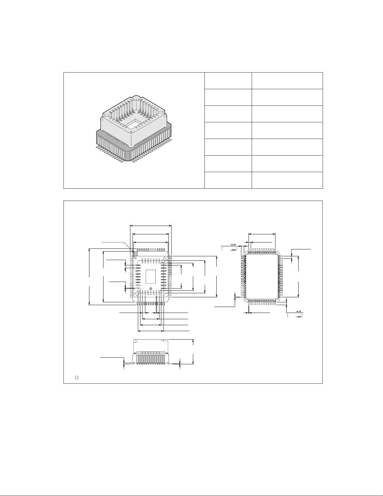
1.6 Package Dimensions
Two types of packages are available for MB89950/950A series. Figure 1.6-1 "FPT-64PM09 package dimensions" and Figure 1.6-2 "MQP-64C-P01 package dimensions" show
the package dimensions.
■ FPT-64P-M09 package dimensions
Figure 1.6-1 FPT-64P-M09 package dimensions
64-pin plastic LQFP Lead pitch 0.65 mm
64-pin plastic LQFP
(FPT-64P-M09)
49
(FPT-64P-M09)
14.00±0.20(.551±.008)SQ
12.00±0.10(.472±.004)SQ
INDEX
Package width
package length
12
12 mm
Lead shape Gullwing
Sealing method Plastic mold
Mounting height 1.70 mm MAX
Note: Pins width and pins thickness include plating thickness.
0.145±0.055
3348
32
(.0057±.0022)
0.10(.004)
0.10(.004)
Details of "A" part
+0.20
1.50
+.008
.059
0.25(.010)
(Mounting height)
10
64
116
0.65(.026)
C
2001 FUJITSU LIMITED F64018S-c-2-4
0.32±0.05
(.013±.002)
17
0.13(.005)
0.50±0.20
"A"
M
(.020±.008)
0.60±0.15
(.024±.006)
Dimensions in mm (inches).
0.10±0.10
(.004±.004)
(Stand off)
Page 25
■ MQP-64C-P01 package dimensions
Figure 1.6-2 MQP-64C-P01 package dimensions
64-pin ceramic MQFP Lead pitch 1.00 mm
CHAPTER 1 OVERVIEW
Lead shape Straight
(MQP-64C-P01)
64-pin ceramic MQFP
(MQP-64C-P01)
INDEX AREA
1.27±0.13
(.050±.005)
22.30±0.33
(.878±.013)
24.70(.972)
TYP
0.30(.012)
TYP
18.70(.736)TYP
16.30±0.33
(.642±.013)
15.58±0.20
(.613±.008)
12.02(.473)
10.16(.400)
TYP
Mounted package
18.12±0.20
(.713±.008)
TYP
14.22(.560)
TYP
Motherboard
material
material
+0.40
1.20
+.016
.047
12.00(.472)TYP
1.00±0.25
(.039±.010)
Ceramic
Plastic
18.00(.709)
1.00±0.25
(.039±.010)
TYP
1.27±0.13
(.050±.005)
0.50(.020)TYP
C
1994 FUJITSU LIMITED M64004SC-1-3
0.30(.012)TYP
7.62(.300)TYP
9.48(.373)TYP
11.68(.460)TYP
10.82(.426)
0.15±0.05
(.006±.002)
MAX
0.40±0.10
(.016±.004)
0.40±0.10
(.016±.004)
Dimensions in mm (inches).
1.20
.047
+0.40
+.016
11
Page 26
CHAPTER 1 OVERVIEW
1.7 I/O Pins and Pin Functions
Table 1.7-1 "Pin description" and Table 1.7-2 "Pin description for external ROM (for
MB89PV950 only)" list the MB89950/950A series I/O pins and their functions. Table 1.7-3
"I/O circuit type" lists the I/O circuit types.
The letter in the "I/O circuit type" column in Table 1.7-1 "Pin description" refer to the
letter in the "Type" column Table 1.7-3 "I/O circuit type".
■ I/O pins and pin functions
Table 1.7-1 Pin description (1/2)
Pin no.
*1
LQFP
22 23 X0
23 24 X1
21 22 MODA B
19 20 RST C
48 to 41 49 to 42
40 to 33 41 to 34
MQFP
*2
Pin name
P00/SEG20
to
P07/SEG27
P10/SEG28
to
P17/SEG35
I/O
circuit
type
A Clock oscillator pins.
Operation mode selection pin.
This pin is connected directly to V
Reset I/O pin.
This pin consists of an N-ch open-drain output with a pull-up
resistor and hysteresis input. A "LOW" level is output from this
pin. A "LOW" voltage on this port generates a RESET condition.
N-channel open-drain type general-purpose I/O ports.
D
D
Also serve as LCD controller/driver segment outputs.
Switching between port output and segment driver output is
performed by the mask option.
N-channel open-drain type general-purpose I/O ports.
Also serve as LCD controller/driver segment outputs.
Switching between port output and segment driver output is
performed by the mask option.
Function
SS
with pull-down resistor.
P20/SEG36
32 to 27 33 to 28
14 to 13 15 to 14 P30 to P31 F N-channel open-drain type general-purpose I/O ports.
12 to 11 13 to 12
15 16 P40 E
12
to
P25/SEG41
P32/V1 to
P33/V2
D
H
N-channel open-drain type general-purpose I/O ports.
Also serve as LCD controller/driver segment outputs.
Switching between port output and segment driver output is
performed by the mask option.
N-channel open-drain type general-purpose I/O ports.
Also serve as LCD controller/driver power supply.
General-purpose I/O port.
A pull-up resistor option is provided.
Page 27

Table 1.7-1 Pin description (2/2)
CHAPTER 1 OVERVIEW
Pin no.
Pin name
LQFP
*1
MQFP
*2
16 17 P41/PWM E
17 18 P42/PWC/INT1 E
18 19 P43/SI E
20 21 P44/SO E
25 26 P45/SCK E
I/O
circuit
type
Function
General-purpose I/O port.
Also serves as PWM timer toggle output (PWM).
A pull-up resistor option is provided.
General-purpose I/O port.
Also serves as pulse-width count timer input (PWC) and external
interrupt input (INT1).
The PWC and INT1 inputs are hysteresis type.
A pull-up resistor option is provided.
General-purpose I/O port.
Also serves as serial I/O and UART data input (SI).
The SI input is hysteresis type.
A pull-up resistor option is provided.
General-purpose I/O port.
Also serves as serial I/O and UART data output (SO).
A pull-up resistor option is provided.
General-purpose I/O port.
Also serves as serial I/O and UART clock input/output (SCK).
The SCK input is hysteresis type.
A pull-up resistor option is provided.
General-purpose input port.
26 27 P46/INT0 E
Also serves as external interrupt input (INT0).
The input is hysteresis type.
A pull-up resistor option is provided.
5 to 1
64 to 57
55 to 49
6 to 1
64 to 58
56 to 50
For LCD segment driver outputs.
SEG0 to SEG19 G
9 to 6 10 to 7 COM0 to COM3 G For LCD common driver outputs.
10 11 V3 - For LCD driver power supply.
56 57
24 25
V
CC
V
SS
Power pin.
-
Power (GND) pin.
-
*1: FPT-64P-M09
*2: MQP-64C-P01
13
Page 28
CHAPTER 1 OVERVIEW
Table 1.7-2 Pin description for external ROM (for MB89PV950 only)
Pin no. Pin name I/O Function
66
67 A12
68 A7
69 A6
70 A5
71 A4
72 A3
73 A2
74 A1
75 A0
77 O1
79 O3
80
82 O4
83 O5
84 O6
85 O7
86 O8
87 CE O
88 A10 O For address output.
89 OE O
91 A11
93 A8
94 A13
95 A14
96
65
76
81
90
V
PP
V
SS
V
CC
N.C. --
O For high-level output.
O For address output.
I For data input.78 O2
O For power supply (GND).
I For data input.
For ROM chip enable.
The High level is output in standby mode.
For ROM output enable.
The Low level is always output.
O For address output.92 A9
O For address output.
O For EPROM power supply.
For internal connection.
Keep open.
14
Page 29
Table 1.7-3 I/O circuit type (1/2)
Type Circuit Remarks
A • Crystal oscillator
X1
N-ch
X0
S
tandby control signal
P-ch
P-ch
N-ch
N-ch
• Feedback resistor: About 1 MΩ (5 V)
B • CMOS input
• Pull-down resistor (N-ch): About 50 kΩ (5 V)
R
CHAPTER 1 OVERVIEW
C • Output pull-up resistor (P-ch): About 50 kΩ (5 V)
• Hysteresis input
R
P-ch
N-ch
D • N-ch open-drain output
• CMOS input
P-ch
N-ch
P-ch
N-ch
N-ch
• The segment driver output is optional.
15
Page 30

CHAPTER 1 OVERVIEW
Table 1.7-3 I/O circuit type (2/2)
Type Circuit Remarks
E • CMOS output
• CMOS input
R
P-ch
P-ch
N-ch
• Hysteresis input (peripheral input)
• The pull-up resistor is optional: About 50 kΩ (5 V)
F • N-ch open-drain output
• CMOS input
N-ch
G • LCD controller/driver common/segment driver
output
P-ch
N-ch
P-ch
N-ch
H • N-ch open-drain output
• CMOS input
P-ch
N-ch
N-ch
16
Page 31

CHAPTER 2
HANDLING DEVICES
This chapter describes points to note when using the
general-purpose single-chip microcontroller.
2.1 "Notes on Handling Devices"
17
Page 32

CHAPTER 2 HANDLING DEVICES
2.1 Notes on Handling Devices
This section lists points to note regarding the power supply voltage, pins, and other
device handling aspects.
■ Notes on handling devices
Preventing latch-up
●
Latch-up may occur on CMOS ICs if voltage higher than V
output pins other than medium to high-voltage pins or if higher than the voltage which shows on Absolute
Maximum Ratings is applied between V
When latch-up occurs, supply current increases rapidly and might thermally damage elements. Take great
care not to exceed the absolute maximum ratings in circuit operation.
Treatment of unused input pins
●
Leaving unused input pins open could cause malfunctions. They should be connected to pull-up or pull-
down resistor.
Power supply voltage fluctuations
●
Although V
therefore cause malfunctions, even if it occurs within the rated range. Stabilizing voltage supplied of the IC
is therefore important. As stabilization guidelines, it is recommended to control power so that V
fluctuations (P-P. value) will be less that 10% of the standard V
to 60 Hz) and the transient fluctuation rate will be less than 0.1 V/ms at the time of a momentary
fluctuation such as when power is switched.
Precaution when using an external clock
●
power supply voltage is assured to operate within the rated, a rapid change to the IC is
CC
and VSS.
CC
or lower than VSS is applied to input and
CC
CC
value at the commercial frequency (50
CC
ripple
18
Even when an external clock is used, oscillation stabilization time is required for power-on reset (option
selection) and release from stop mode.
Page 33

Recommended screening conditions
●
The OTPROM product should be screened by high-temperature aging before mounting.
High-temperature aging (150 C, 48Hrs)
The programming test cannot be performed for all bits of the preprogrammed OTPROM product due to its
characteristics. Consequently, 100% programming yielding cannot be ensured.
Treatment of N.C. pins
●
Be sure to leave (internally connected) N.C. pins open.
CHAPTER 2 HANDLING DEVICES
Verify program
Read
Mount
Unused LCD controller/driver dedicated pins
●
When LCD controller/driver dedicated pins are not in use, keep it open.
Port shared with SEG pin
●
When using port shared with SEG pin, be sure that the input voltage to port does not exceed the voltage of
V3 (SEG driving voltage). When power-on or reset, SEG pin will output an initial value of "L".
LCD controller/driver not in use
●
When LCD controller/driver is not in use, connect the V3 pin to V
dedicated pins open.
and keep other LCD controller/driver
CC
19
Page 34

CHAPTER 2 HANDLING DEVICES
20
Page 35

CHAPTER 3
CPU
This chapter describes the functions and operation of
the CPU.
3.1 "Memory Space"
3.2 "Dedicated Registers"
3.3 "General-purpose Registers"
3.4 "Interrupts"
3.5 "Resets"
3.6 "Clocks"
3.7 "Standby Modes (Low-power Consumption)"
3.8 "Memory Access Mode"
21
Page 36

CHAPTER 3 CPU
3.1 Memory Space
The microcontrollers of the MB89950/950A series offer a memory space of 64 Kbytes.
The memory space contains the I/O area, RAM area, ROM area, and external area. The
memory space contains areas used for special purposes such as the general-purpose
registers and vector table.
■ Memory space structure
I/O area (addresses: 0000H to 007FH)
●
• Control registers and data registers for the internal peripheral functions are located in this area.
• As the I/O area is allocated within the memory space, I/O can be accessed in the same way as memory.
High-speed access using direct addressing is available.
RAM area
●
ROM area
●
• Internal static RAM is provided as an internal data area.
• The internal RAM size differs from product to product.
• Addresses between 0080
• Addresses between 0100
apply for some products).
• The contents of RAM is indeterminate after a reset.
• Internal ROM is provided as an internal program area.
• The internal ROM size differs from product to product.
• Addresses between FFC0
and 00FFH support high-speed access using direct addressing.
H
and 01FFH can be used as the general-purpose register area (restrictions
H
and FFFFH are used for the vector table, etc.
H
22
Page 37

■ Memory map
CHAPTER 3 CPU
Figure 3.1-1 Memory map
0000
0080
00C0
0100
0140
F000
FFC0
FFFF
MB89951A
H
H
Reserved
H
RAM
H
Registers
H
Access
prohibited
H
ROM
H
H
I/O
0000
0080
0100
0180H
E000
FFC0
FFFF
MB89953A
H
I/O
H
RAM
H
Registers
Access
prohibited
H
ROM
H
H
Vector table
0000
0080
0100
0200H
0280
MB89P955
H
H
RAM
H
Registers
H
I/O
0000
0080
0100
0200H
MB89PV950
H
I/O
H
RAM
H
Registers
0480H
C000
FFC0
FFFF
H
H
H
Access
prohibited
ROM
8000
FFC0
FFFF
H
H
H
Access
prohibited
ROM
(reset, interrupt, vector call instruction)
23
Page 38

CHAPTER 3 CPU
3.1.1 Special Areas
In addition to the I/O area, the special purpose areas in the memory space include the
general-purpose register area and the vector table area.
■ General-purpose register areas (addresses: 0100H to 01FFH)
• Provides auxiliary registers for 8-bit arithmetic operation and transfer instructions.
• Allocated to a region of the RAM area. Can also be used as normal RAM.
• Using the area as general-purpose registers enables high-speed access by general-purpose register
addressing using short instructions.
Table 3.1-1 "General-purpose register areas" lists the areas in each device that can be used for general-
purpose registers.
Table 3.1-1 General-purpose register areas
Part number MB89951A MB89953A MB89P955/PV950
Number of banks 8 16 32
Address range 0100
See section 3.2.2 "Register Bank Pointer (RP)" and section 3.3 "General-purpose Registers" for details.
to 013F
H
H
0100H to 017F
H
0100H to 01FF
H
24
Page 39

■ Vector table area (addresses: FFC0H to FFFFH)
• Used as the vector table for the vector call instruction, interrupts, and resets.
• The vector table is allocated at the top of the ROM area. The start address of the corresponding
processing routine is set as data at each vector table address.
Table 3.1-2 "Vector table" lists the vector table addresses referenced by the vector call instruction,
interrupts, and resets.
See Section 3.4 "Interrupts", Section 3.5 "Resets", and "(6) CALLV #vct" in Appendix B.2, "Special
Instructions" for details.
Table 3.1-2 Vector table
CHAPTER 3 CPU
Vector call
instruction
Vector table address
Upper Lower Upper Lower
CALLV #0 FFC0
CALLV #1 FFC2
CALLV #2 FFC4
CALLV #3 FFC6
CALLV #4 FFC8
CALLV #5 FFCA
CALLV #6 FFCC
CALLV #7 FFCE
Vector table address
Interrupts
H
H
H
H
H
H
H
H
FFC1
FFC3
FFC5
FFC7
FFC9
FFCB
FFCD
FFCF
H
H
H
H
H
H
H
H
IRQB FFE4
IRQA FFE6
IRQ9 FFE8
IRQ8 FFEA
IRQ7 FFEC
IRQ6 FFEE
IRQ5 FFF0
IRQ4 FFF2
IRQ3 FFF4
IRQ2 FFF6
IRQ1 FFF8
IRQ0 FFFA
H
H
H
H
H
H
H
H
H
H
H
H
FFE5
FFE7
FFE9
FFEB
FFED
FFEF
FFF1
FFF3H
FFF5
FFF7
FFF9
FFFB
H
H
H
H
H
H
H
H
H
H
H
Mode data
Reset vector FFFE
--
(*1)
H
*1: FFFCH is not available. (Set FFH.)
FFFD
FFFF
H
H
25
Page 40

CHAPTER 3 CPU
3.1.2 Storing 16-bit Data in Memory
For 16-bit data and the stack, store the upper data in the lower memory address value.
■ Storing 16-bit data in RAM
When writing 16-bit data to memory, store the upper byte at the lower address and the lower byte at the
next address. Handle reading of 16-bit data in the same way.
Figure 3.1-2 "Storing 16-bit data in memory" shows how 16-bit data is stored in memory.
Figure 3.1-2 Storing 16-bit data in memory
Memory Memory
Before execution
Before execution
1 2 3 4 H
1 2 3 4 H
A
A
Memory Memory
MOVW 0081H,A
MOVW 0081H,A
0080
0080
H
H
0081
0081
H
H
0082
0082
H
H
0083H
0083H
After execution
After execution
1 2 3 4 H
1 2 3 4 H
A
A
12H
12H
34H
34H
0080
0080
0081
0081
0082
0082
0083H
0083H
H
H
H
H
H
H
■ Storing 16-bit operands
The same byte order applies when specifying a 16-bit operand in an instruction. Store the upper byte at the
address following the operation code (instruction) and the lower byte at the next address.
The byte ordering applies to both 16-bit immediate data and operands that specify a memory address.
Figure 3.1-3 "Byte order of 16-bit data in an instruction" shows how 16-bit data is stored in an instruction.
Figure 3.1-3 Byte order of 16-bit data in an instruction
[Example] MOV A,5678H ; Extended address
MOVW A,#1234H ; 16-bit immediate data
X X X 0 H XX XX
X X X 2
X X X 5
X X X 8
■ Storing 16-bit data on stack
The same byte order applies when saving 16-bit register data on the stack during an interrupt or similar.
The upper byte is stored in the lower address.
After assembly
.
.
.
H 60 56 78 ; Extended address
H E4 12 34 ; 16-bit immediate data
H XX
.
.
.
26
Page 41
CHAPTER 3 CPU
3.2 Dedicated Registers
The dedicated registers in the CPU consist of the program counter (PC), two arithmetic
operation registers (A and T), three address pointers (IX, EP, and SP), and the program
status (PS). All registers are 16 bits.
■ Dedicated register configuration
The dedicated registers in the CPU consist of seven 16-bit registers. Some of these registers are also able to
be used as 8-bit register, using the lower 8 bits only.
Figure 3.2-1 "Dedicated register configuration" shows the structure of the dedicated registers.
Figure 3.2-1 Dedicated register configuration
Initial value
FFFD
H
Indeterminate
Indeterminate
Indeterminate
Indeterminate
Indeterminate
I-flag = "0"
IL0, IL1 = "11"
Otherbits are indeterminate
16 bits
RP CCR
■ Dedicated register functions
Program counter (PC)
●
The program counter is a 16-bit counter that indicates the memory address of the instruction currently
being executed by the CPU. Instruction execution, interrupts, resets, and similar update the contents of the
program counter. The initial value during a reset is the read address of the mode data (FFFD
PC
A
T
IX
EP
SP
PS
: Program counter
A register for indicating the current instruction
storage positions
: Accumulator
A temporary register for storing arithmetic operations or
transfer instructions
: Temporary accumulator
A register for performing arithmetic operations with
the accumulator
: Index register
A register for indicating an index address
: Extra pointer
A pointer for indicating a memory address
: Stack pointer
A register for indicating the current stack location
: Program status
A register for storing a register bank pointer and
condition code
).
H
Accumulator (A)
●
The accumulator is a 16-bit arithmetic operation register. The accumulator is used to perform arithmetic
operations and data transfers with data in memory or in other registers such as the temporary accumulator
(T). The content of the accumulator can be treated as either word (16-bit) or byte (8-bit) data. Only the
lower 8 bits (AL) of the accumulator are used for byte arithmetic operations or transfers. In this case, the
upper 8 bits (AH) remain unchanged. The content of the accumulator after a reset is indeterminate.
27
Page 42

CHAPTER 3 CPU
Temporary accumulator (T)
●
The temporary accumulator is an auxiliary 16-bit arithmetic operation register used to perform arithmetic
operations with the data in the accumulator (A). The content of the temporary accumulator is treated as
word data (16-bit) for word-length arithmetic operations with the accumulator and as byte data (8-bit) for
byte-length arithmetic operations. For byte-length arithmetic operations, only the lower 8 bits of the
temporary accumulator (TL) are used and the upper 8 bits (TH) are not used.
Executing a transfer instruction to transfer data to the accumulator (A) automatically transfer the previous
content of the accumulator to the temporary accumulator. In this case also, a byte transfer leaves the upper
8 bits of the temporary accumulator (TH) unchanged. The content of the temporary accumulator after a
reset is indeterminate.
Index register (IX)
●
The index register is a 16-bit register used to hold the index address. The index register is used in
conjunction with a single byte offset value (-128 to +127). Adding the sign-extended offset value to the
index address generates the memory address for data access. The content of the index register after a reset
is indeterminate.
Extra pointer (EP)
●
The extra pointer is a 16-bit register used to hold a memory address for data access. The content of the
extra pointer after a reset is indeterminate.
Stack pointer (SP)
●
The stack pointer is a 16-bit register used to hold the address referenced during operations such as
interrupts, subroutine calls, and the stack save and restore instructions. The value of the stack pointer
during program execution is the address of the most recently saved data on the stack. The content of the
stack pointer after a reset is indeterminate.
Program status (PS)
●
The program status is a 16-bit control register. The upper 8 bits contain the register bank pointer (RP)
which points to the address of the current general-purpose register bank.
The lower 8 bits contain the condition code register (CCR) which contains flags indicating the current CPU
status. The two 8-bit registers which form the program status cannot be accessed independently (the
program status can only be accessed by the MOVW A,PS and MOVW PS,A instructions).
Refer to the F
2
MC-8L MB89600 series Programming Manual for details on using the dedicated registers.
28
Page 43

CHAPTER 3 CPU
3.2.1 Condition Code Register (CCR)
The condition code register (CCR) located in the lower 8 bits of the program status (PS)
consists of the C, V, Z, N, and H bits indicating the results of arithmetic operations and
the contents of transfer data, and the I, IL1, and IL0 bits for control whether or not the
CPU accepts interrupt requests.
■ Structure of condition code register (CCR)
Figure 3.2-2 Structure of condition code register
RP CCR
Bit 15 Bit 14 Bit 13 Bit 12 Bit 11 Bit 10 Bit 9 Bit 8 Bit 7 Bit 6 Bit 5 Bit 4 Bit 3 Bit 2 Bit 1 Bit 0
R4 R3 R2 R1 R0 ——— HIIL1IL0NZVC
PS
Half-carry flag
Interrupt enable flag
Interrupt level bits
Negative flag
Zero flag
X: Indeterminate
- : Unused
Overflow flag
Carry flag
CCR initial value
X011XXXX
B
■ Arithmetic operation result bits
Half-carry flag (H)
●
Set to "1" when a carry from bit 3 to bit 4 or a borrow from bit 4 to bit 3 occurs as a result of an arithmetic
operation. Clear to "0" otherwise. As this flag is for the decimal adjustment instructions, do not use this flag
in cases other than addition or subtraction.
Negative flag (N)
●
Set to "1" if the most significant bit (MSB) is set to "1" as a result of an arithmetic operation. Clear to "0"
when the bit is set to "0".
Zero flag (Z)
●
Set to "1" when an arithmetic operation results in "0". Clear to "0" otherwise.
Overflow flag (V)
●
Set to "1" if a signed numeric value overflows because of an arithmetic calculation. Clear to "0" if the
overflow does not occur.
29
Page 44

CHAPTER 3 CPU
Carry flag (C)
●
Set to "1" when a carry from bit 7 or borrow to bit 7 occurs as a result of an arithmetic operation. Clear to
"0" otherwise. Set to the shift-out value in case of a shift instruction.
Figure 3.2-3 "Change of carry flag by shift instruction" shows the change of the carry flag by a shift
instruction.
Left shift (ROLC) Right shift (RORC)
C
Note:
Reference:
Figure 3.2-3 Change of carry flag by shift instruction
Bit 7 Bit 0
Bit 7 Bit 0
C
The condition code register is part of the program status (PS) and cannot be accessed independently.
In practice, the flag bits are rarely fetched and used directly. Instead, the bits are used indirectly by
instructions such as branch instructions (such as BNZ) or the decimal adjustment instructions (DAA,
DAS). The content of the flags after a reset is indeterminate.
■ Interrupt acceptance control bit
Interrupt enable flag (I)
●
Interrupt is enabled when this flag is set to "1" and the CPU accepts interrupt. Interrupt is prohibited when
this flag is set to "0" and the CPU does not accept interrupt.
The initial value after a reset is "0".
Normal practice is to set the flag to "1" by the SETI instruction and clear to "0" by the CLRI instruction.
Interrupt level bits (IL1, IL0)
●
These bits indicate the level of the interrupt currently being accepted by the CPU. The value is compared
with the interrupt level setting registers (ILR1 to ILR3) which have a setting for each peripheral function
interrupt request (IRQ0 to IRQB).
Given that the interrupt enable flag is enabled (I = "1"), the CPU only performs interrupt processing for
interrupt requests with an interrupt level value that is less than the value of these bits. Table 3.2-1 "Interrupt
level" lists the interrupt level priorities. The initial value after a reset is "11
Table 3.2-1 Interrupt level
IL1 IL0 Interrupt level Priority
00
01
".
B
1
High
30
10 2
11 3
Low (no interrupt)
Page 45

Reference:
CHAPTER 3 CPU
The interrupt level bits (IL1, IL0) are normally "11
(during main program execution).
See Section 3.4 "Interrupts" for details on interrupts.
" when the CPU is not processing an interrupt
B
31
Page 46

CHAPTER 3 CPU
3.2.2 Register Bank Pointer (RP)
The register bank pointer (RP) located in the upper 8 bits of the program status (PS)
indicates the address of the general-purpose register bank currently in use. The RP is
converted to form the actual address in general-purpose register addressing.
■ Structure of register bank pointer (RP)
Figure 3.2-4 "Structure of register bank pointer" shows the structure of the register bank pointer.
Figure 3.2-4 Structure of register bank pointer
RP CCR
Bit 15 Bit 14 Bit 13 Bit 12 Bit 11 Bit 10 Bit 9 Bit 8 Bit 7 Bit 6 Bit 5 Bit 4 Bit 3 Bit 2 Bit 1 Bit 0
R4 R3 R2 R1 R0 ——— HIIL1IL0NZVC
PS
X: Indeterminate
- : Unused
RP initial value
XXXXXXXX
B
The register bank pointer indicates the address of the register bank currently in use. Figure 3.2-5 "Rule for
conversion of actual addresses of general-purpose register area" shows the relationship between the pointer
contents and the actual address is based on the conversion rule.
Figure 3.2-5 Rule for conversion of actual addresses of general-purpose register area
Upper bits of RP Lower operation codes
"0" "0" "0" "0" "0" "0" "0" "1" R4 R3 R2 R1 R0 b2 b1 b0
Generated addresses
A15 A14 A13 A12 A10 A11 A9 A8 A7 A6 A5 A4 A3 A2 A1 A0
The register bank pointer points to the memory block (register bank) in the RAM area that is used for
general-purpose registers. A total of 32 register banks are available. A register bank is specified by setting a
value between 0 and 31 in the upper 5 bits of the register bank pointer. Each register bank contains eight 8-
bit general-purpose registers. Registers are specified by the lower 3 bits of the operation codes.
Using the register bank pointer, the addresses 0100
to 01FFH can be used as the general-purpose register
H
area. However, the available area is limited on some products if internal RAM only is used. The initial
value after a reset is indeterminate.
Note:
32
The register bank pointer is part of the program status (PS) and cannot be accessed independently.
Page 47

CHAPTER 3 CPU
3.3 General-purpose Registers
The general-purpose registers are a memory block made up of banks, with 8 x 8-bit
registers per bank.
The register bank pointer (RP) is used to specify the register bank.
The function permits the use of up to 32 banks, but the number of banks that can
actually be used depends on how much RAM the device has.
Register banks are valid for interrupt processing, vector call processing, and
subroutine calls.
■ Structure of general-purpose registers
• The general-purpose registers are 8 bits and located in the register banks of the general-purpose register
area (in RAM).
• One bank contains eight registers (R0 to R7) and up to a total of 32 banks. However, the number of
banks available for general-purpose registers is limited on some products if internal RAM only is used.
• The register bank currently in use is specified by the register bank pointer (RP). The lower three bits of
the operation code specify general-purpose register 0 (R0) to general-purpose register 7 (R7).
Figure 3.3-1 "Register bank structure" shows the register bank structure.
Figure 3.3-1 Register bank structure
Lower 3 bits of
the operation code
R0
R1
R2
R3
R4
R5
R6
R7
R0
R7
000
001
010
011
100
101
110
111
000
:
:
111
:
:
:
:
:
:
Bank 0
(RP="00000---
Bank 1
(RP="00001---
Bank 2
to
Bank 30
B")
B")
32 banks
(RAM area)
The number of banks is limited
on available RAM size.
100
108
H*
H*
1F8H*
1FFH
*: The top address of a register bank = 0100
000
R0
:
:
111
R7
H + 8 x (upper 5 bits of RP)
Bank 31
(RP="11111---
)
B"
See Section 3.1.1 "Special Areas" for the general-purpose register area available for each product.
33
Page 48

CHAPTER 3 CPU
■ Features of general-purpose registers
General-purpose registers have the following features:
• RAM can be accessed at high-speed using short instructions (general-purpose register addressing).
• Registers are grouped in blocks in the form of register banks. This simplifies the process of saving
register contents and dividing registers by function.
Dedicated register banks can be permanently assigned for each interrupt processing or vector call (CALLV
#0 to #7) processing routine by general-purpose register. For example, register bank 4 interrupt 2.
For example, a particular interrupt processing routine only uses a particular register bank which cannot be
written to unintentionally by other routines. The interrupt processing routine only needs to specify its
dedicated register bank at the start of the routine to effectively save the general-purpose registers in use
prior to the interrupt. Therefore, saving the general-purpose registers to the stack or other memory location
is not necessary. This allows high-speed interrupt handling while maintaining simplicity.
Also, as an alternative to saving general-purpose registers in subroutine calls, register banks can be used to
create reentrant programs (programs that do not use fixed addresses and can be entered more than once)
usually made by the index register (IX).
Note:
If an interrupt processing routine changes the register bank pointer (RP), ensure that the program does
not also change the interrupt level bits in the condition code register (CCR: IL1, IL0) when specifying
the register bank.
34
Page 49

CHAPTER 3 CPU
3.4 Interrupts
The MB89950/950A series has 12 interrupt request inputs corresponding to peripheral
functions. The interrupt level can be set independently.
If an interrupt request output is enabled in the peripheral function, an interrupt request
from a peripheral function is compared with the interrupt level in the interrupt
controller. The CPU performs interrupt operation according to how the interrupt is
accepted. The CPU wakes up from standby mode, and returns to the interrupt or normal
operation.
■ Interrupt requests from peripheral functions
Table 3.4-1 "Interrupt request and interrupt vector" lists the interrupt requests corresponding to the
peripheral functions. On acceptance of an interrupt, execution branches to the interrupt processing routine.
The contents of interrupt the vector table address corresponding to the interrupt request specifies the branch
destination address for the interrupt processing routine.
An interrupt processing level can be for each interrupt request in the interrupt level setting registers (ILR1,
ILR2, ILR3). Three levels are available.
If an interrupt request with the same or lower level occurs during execution of an interrupt processing
routine, the latter interrupt is not normally processed until the current interrupt processing routine
completes. If interrupt request set the same level occur simultaneously, the highest priority is IRQ0.
Table 3.4-1 Interrupt request and interrupt vector
Interrupt request
IRQ0 (External interrupt 0)
IRQ1 (External interrupt 1)
IRQ2 (8-bit PWM timer)
IRQ3 (PWC)
IRQ4 (UART)
IRQ5 (8-bit serial I/O)
IRQ6 (Timebase timer)
IRQ7 (Unused)
Vector table address Bit names of the
interrupt level
Upper Lower
FFFA
FFF8
FFF6
FFF4
FFF2
FFF0
FFEE
FFEC
H
H
H
H
H
H
H
H
FFFB
FFF9
FFF7
FFF5
FFF3
FFF1
FFEF
FFED
H
H
H
H
H
H
H
H
setting register
L01, L00
L11, L10
L21, L20
L31, L30
L41, L40
L51, L50
L61, L60
L71, L70
Priority
(*1)
High
IRQ8 (Unused)
IRQ9 (Unused)
IRQA (Unused)
IRQB (Unused)
*1: This priority is applied when interrupts of the same level occur simultaneously.
FFEA
FFE8
FFE6
FFE4
H
H
H
H
FFEB
FFE9
FFE7
FFE5
H
H
H
H
L81, L80
L91, L90
LA1,LA0
LB1, LB0
Low
35
Page 50

CHAPTER 3 CPU
3.4.1 Interrupt Level Setting Registers (ILR1, ILR2, ILR3)
The interrupt level setting registers (ILR1, ILR2, ILR3) together contain 12 blocks of 2-bit
data, with each data corresponding to an interrupt request from a peripheral function.
The interrupt level for each interrupt is set in that interrupt’s corresponding 2-bit data
(interrupt level setting bits).
■ Structure of interrupt level setting registers (ILR1, ILR2, ILR3)
Figure 3.4-1 Structure of interrupt level setting registers
Register Address Bit 7 Bit 6 Bit 5 Bit 4 Bit 3 Bit 2 Bit 1 Bit 0 Initial value
ILR1 007C
L31 L30 L21 L20 L11 L10
H
W WWWWWWW
L01
L00 11111111
B
ILR2 007D
ILR3 007EH
W: Write-only
L71 L70
H
W WWWWWWW
LB1 LB0 LA1 LA0 L91
W WWWWWWW
L61
L60 L51 L50 L41 L40 11111111
L90
L81 L80 11111111
B
B
Two bits of the interrupt level setting registers are allocated to each interrupt request. The value of the
interrupt level setting bits in these registers sets the interrupt priority (interrupt levels 1 to 3).
The interrupt level setting bits are compared with the interrupt level bits in the condition code register
(CCR: IL1, IL0).
The CPU does not accept interrupt requests set to interrupt level 3.
Table 3.4-2 "Interrupt level setting bit and interrupt level" shows the relationship between the interrupt
level setting bits and the interrupt levels.
Table 3.4-2 Interrupt level setting bit and interrupt level
L01 to LB1 L00 to LB0
Interrupt
request level
Priority
00
1
High
01
36
10 2
11 3
Low (no interrupt)
Reference:
The interrupt level bits in the condition code register (CCR: IL1, IL0) are normally "11
" during main
B
program execution.
Note:
As the IRL1, ILR2, and ILR3 registers are write-only, the bit manipulation instructions cannot be used.
Page 51

CHAPTER 3 CPU
3.4.2 Interrupt Processing
The interrupt controller transmits the interrupt level to the CPU when an interrupt
request is generated by a peripheral function. If the CPU is able to receive the interrupt,
the CPU temporarily halts the currently executing program and executes the interrupt
processing routine.
■ Interrupt processing
The procedure for interrupt operation is performed in the following order: interrupt source generated at
peripheral function, set the interrupt request flag bit (request FF), discriminate the interrupt request enable
bit (enable FF), the interrupt level (ILR1, ILR2, ILR3 and CCR: IL1, IL0), simultaneously generated
interrupt requests with the same level, then check the interrupt enable flag (CCR: I). Figure 3.4-2 "Interrupt
processing" shows the interrupt processing.
Figure 3.4-2 Interrupt processing
Condition code
register (CCR)
PS I IL
IR
Check
F2MC-8L CPU
Comparator
(5)
(4)
Wake-up from
stop mode
Wake-up from
sleep mode
Exit watch mode
START
(1)
Initialize peripheral
Internal bus
Register
file
IPLA
(7)
(6)
RAM
Is an interrupt
request present at the
peripheral?
NO
Main program
(2)
execution
(7)
Restore PC and PS
YES
Is interrupt
request output enabled
for the peripheral?
NO
(4)
Interrupt processing routine
Clear interrupt request
Execute interrupt processing
Enable FF
Request FF
(3)
Peripherals
(3)
YES
Check the interrupt priority level
and transfer the level to the CPU
Compare the level with
the IL bits in PS
Is the level
higher than IL?
NO
RETI
AND
YES
I-flag = 1?
NO
Interrupt
Level comparator
controller
YES
Save PC and PS to the stack
(6)
PC interrupt vector
Update IL in PS
(5)
37
Page 52

CHAPTER 3 CPU
1. After a reset, all interrupt requests are disabled.
2. Execute the main program (for multiple interrupts, execute the interrupt processing routine).
3. The interrupt request flag bit (request FF) for a peripheral function is set to "1" when the peripheral
4. The interrupt controller continuously monitors for interrupt requests from the peripheral functions and
5. If the interrupt level received by the CPU has a higher priority (a lower level value) than the level set in
- Initialize the peripheral functions that are to generate interrupts in the peripheral function
initialization program, set the interrupt levels in the appropriate interrupt level setting registers (ILR1,
ILR2, ILR3), and start peripheral function.
- The interrupt level can be set to 1, 2 or 3. Level 1 is the highest priority, followed by level 2. Setting
level 3 disables the interrupt for that peripheral function.
function generates an interrupt source. If the interrupt request enable bit for the peripheral function is set
to "enable" (enable FF = "1"), the peripheral function outputs the interrupt request to the interrupt
controller.
passes the interrupt level of the current interrupt request with the highest interrupt level to the CPU. The
interrupt controller also evaluates the priority order if requests with the same level are present
simultaneously.
the interrupt level bits in the condition code register (CCR: IL1, IL0), the CPU checks the interrupt
enable flag (CCR: I) and receives the interrupt if interrupts are enabled (CCR: I = "1").
6. The CPU saves the contents of the program counter (PC) and program status (PS) on the stack, reads the
top address of the interrupt processing routine from the interrupt vector table for the interrupt, updates
the interrupt level bits in the condition code register (CCR: IL1, IL0) with the received interrupt level,
and starts execution of the interrupt processing routine.
7. Finally, on execution of the RETI instruction, the CPU restores the program counter (PC) and program
status (PS) values saved on the stack and resumes execution from the instruction following the last
instruction executed before the interrupt.
Note:
As the interrupt request flag bit of a peripheral function is not cleared automatically when an interrupt
request is received, the bit must be cleared by the program (normally, by writing "0" to the interrupt
request flag bit) at interrupt processing routine.
An interrupt wakes up the CPU from standby mode (low-power consumption). See Section 3.7 "Standby
Modes (Low-power Consumption)" for details.
Reference:
If the interrupt request flag bit is cleared at the top of the interrupt processing routine, the peripheral
function that has generated the interrupt becomes able to generate another interrupt during execution of
the interrupt processing routine (resetting the interrupt request flag bit). However, the interrupts are not
normally accepted until the current processing routine completes.
38
Page 53

CHAPTER 3 CPU
3.4.3 Multiple Interrupts
Multiple interrupts can be performed by setting different interrupt levels to the interrupt
level setting register for two or more interrupt requests from peripheral functions.
■ Multiple interrupts
If the interrupt request having the higher interrupt levels occurs during the interrupt processing routines, the
CPU halts the current interrupt process and switches to accept the interrupt with the higher priority.
Interrupt levels can be set in the range 1 to 3. However, the CPU does not accept interrupt requests set to
interrupt level 3.
Example of multiple interrupts
●
As an example of multiple interrupt processing, assume that an external interrupt has a higher priority than
the timer interrupt. The timer interrupt is set to level 2 and the external interrupt is set to level 1. Figure 3.4-
3 "Example of multiple interrupts" shows the processing when the external interrupt occurs during
execution of timer interrupt processing.
Figure 3.4-3 Example of multiple interrupts
Main program
Initialize peripheral
Timer interrupt occurs
Restart main program
(1)
(2)
(8)
Interrupt level 2
(CCR:IL1, IL0 = "10")
Timer interrupt processing
(3)
External interrupt
occurs
Halt
Restart
Timer interrupt
processing
(7)
Timer interrupt returns
External interrupt processing
Interrupt level 1
(CCR:IL1, IL0 = "01")
(4)
(5)(6)
External interrupt
processing
External interrupt
returns
• During execution of timer interrupt processing, the interrupt level bits in the condition code register
(CCR:IL1, IL0) are automatically set to the same value as the interrupt level setting register (ILR1,
ILR2, ILR3) corresponding to the timer interrupt (level 2 in this example). If the interrupt request set to
higher interrupt level (level 1 in this example) occurs at this time, the interrupt processing has priority.
• To temporarily disable multiple interrupts during the timer interrupt, the interrupt enable flag in the
condition code register is set to "interrupts disabled" (CCR: I = "0") or the interrupt level bits (IL1, IL0)
set to "00
".
B
• On execution of the interrupt return instruction (RETI) at the completion of interrupt processing, the
CPU restores the program counter (PC) and program status (PS) values saved on the stack and resumes
execution of the interrupted program.
Restoring the program status (PS) returns the condition code register (CCR) to the value prior to the
interrupt.
39
Page 54

CHAPTER 3 CPU
3.4.4 Interrupt Processing Time
The total time from the generation of an interrupt request until control passes to the
interrupt processing routine is the sum of the time required to complete execution of
the current instruction and the interrupt handling time (the time required to prepare for
interrupt processing). The maximum time for this process is 30 instruction cycles.
■ Interrupt processing time
When an interrupt request occurs, the time until the interrupt is accepted and the interrupt processing
routine is executed includes the interrupt request sampling time and the interrupt handling time.
Interrupt request sampling time
●
Whether or not an interrupt request has occurred is determined by sampling and testing for interrupt
requests during the final cycle of each instruction. Therefore, the CPU is unable to identify interrupt
requests during execution of an instruction. The longest delay occurs when an interrupt request is generated
immediately after starting execution of a DIVU instruction, which has the longest instruction cycles (21
instruction cycles).
Interrupt handling time
●
Nine instruction cycles are required to perform the following preparation for interrupt processing after the
CPU accepts an interrupt request:
• Save the program counter (PC) and program status (PS).
• Set the top address of the interrupt processing routine (the interrupt vector) in the PC.
• Update the interrupt level bits (PS: CCR: IL1, IL0) in the program status (PS).
Figure 3.4-4 "Interrupt processing time" shows the interrupt processing time.
CPU operation
Interrupt waiting time
: Final cycle of instruction. Interrupt requests are sampled at this timing.
The total interrupt processing time of 21 + 9 = 30 instruction cycles is required if an interrupt request
occurs immediately after starting execution of a DIVU instruction, which has the longest instruction cycles
(21 instruction cycles). If, on the other hand, the program does not use the DIVU or MULU instructions,
the maximum interrupt processing time is 6 + 9 = 15 instruction cycles.
Figure 3.4-4 Interrupt processing time
Execution of a standard instruction
Interrupt request
sampling time
Interrupt request occurs
Interrupt handling
Interrupt handling time
(9 instruction cycles)
Interrupt processing routine
40
The time of one instruction cycle changes with the clock mode and the main clock frequency as selected by
the "speed-shift" (gear) function. See Section 3.6 "Clocks" for details.
Page 55

CHAPTER 3 CPU
3.4.5 Stack Operation during Interrupt Processing
This section describes the saving of the register contents to the stack and restore
operation during interrupt processing.
■ Stack operation at start of interrupt processing
The CPU automatically saves the current contents of the program counter (PC) and program status (PS) to
the stack when an interrupt is accepted.
Figure 3.4-5 "Stack operation at start of interrupt processing" shows the stack operation at the start of
interrupt processing.
Figure 3.4-5 Stack operation at start of interrupt processing
Immediately before
interrupt
Address Memory
PS
PC
0870
E000
SP
H
H
0280
027C
027D
027E
027F
0280
H
0281
XXH
H
XXH
H
XXH
H
XXH
H
XXH
H
XXH
H
■ Stack operation at interrupt return
On execution of the interrupt return instruction (RETI) at the completion of interrupt processing, the CPU
performs the opposite processing to interrupt initiation, restoring first the program status (PS) and then the
program counter (PC) from the stack. This returns the PS and PC to their states immediately prior to the
start of the interrupt.
Note:
The CPU does not automatically save the accumulator (A) or temporary accumulator (T) contents to the
stack. Use the PUSHW and POPW instructions to save and restore A and T contents to and from the
stack.
PS
PC
Immediately after
interrupt
027C
SP
0870
H
E000
H
H
Address Memory
027C
027D
027E
027F
0280
0281
08
H
H
70
H
H
E0
H
H
00
H
H
H
XXH
H
XXH
PS
PC
41
Page 56

CHAPTER 3 CPU
3.4.6 Stack Area for Interrupt Processing
Interrupt processing execution uses the stack area in RAM. The contents of the stack
pointer (SP) specifies the top address of the stack area.
■ Stack area for interrupt processing
The subroutine call instruction (CALL) and vector call instruction (CALLV) use the stack area to save and
restore the program counter (PC). The stack area is also used by the PUSHW and POPW instructions to
temporarily save and restore registers.
• The stack area is located in RAM along with the data area.
• Initializing the stack pointer (SP) to the top address of RAM and allocating data areas upwards from the
bottom RAM address is recommended.
Figure 3.4-6 "Stack area for interrupt processing" shows the example of stack area setting.
Figure 3.4-6 Stack area for interrupt processing
0000
H
H
H
H
RAM
Generalpurpose
registers
Access
prohibited
ROM
I/O
Recommended set value for SP
(When the top address of RAM is 0280
H.)
Data area
Stack area
0080
0100
0200
0280H
FFFFH
Note:
The stack area is used in the downward direction starting from a high address by functions such as
interrupts, subroutine calls, and the PUSHW instruction. Instructions such as return instructions (RETI,
RET) and the POPW instruction release stack area in the upward direction. Take care when the stack
address is decreased by multiple interrupts or subroutine calls that the stack does not overlap the
general-purpose register area or areas containing other data.
42
Page 57

CHAPTER 3 CPU
3.5 Resets
The MB89950/950A series supports the following four types of reset source:
• External reset
• Software reset
• Watchdog reset
• Power-on reset (optional)
At reset, main clock oscillation stabilization delay time may or may not occur by the
operating mode and option settings.
■ Reset source
Table 3.5-1 Reset source
Reset source Reset condition
External reset Set the external reset pin to the "L" level.
Software reset Write "0" to the software reset bit in the standby control register (STBC: RST).
Watchdog reset Watchdog timer overflow.
Power-on reset Power is turned on (only on products with a power-on reset).
External reset
●
Inputting an "L" level to the external reset pin (RST
the "H" level wakes up the CPU from the external reset.
When power is turned on to products with power-on reset or for external resets in stop mode, the reset
operation is performed after the oscillation stabilization delay time has passed and the CPU wakes up from
the external reset. External resets on products without power-on reset do not wait for the oscillation
stabilization delay time.
The external reset pin can also function as a reset output pin (optional).
Software reset
●
Writing "0" to the software reset bit in the standby control register (STBC: RST) generates a four-
instruction-cycle reset. The software reset does not wait for the oscillation stabilization delay time.
) generates an external reset. Returning the reset pin to
Watchdog reset
●
The watchdog reset generates a four-instruction-cycle reset if data is not written to the watchdog timer
control register (WDTC) within a fixed time after the watchdog timer starts. The watchdog reset does not
wait for the oscillation stabilization delay time.
43
Page 58

CHAPTER 3 CPU
Power-on reset
●
Products can be set to with or without power-on reset (optional). On products with power-on reset, turning
on the power generates a reset. The reset operation is performed after the oscillation stabilization delay time
has passed. Moreover, external reset signal is outputted by the reset output option.
On products without power-on reset, an external reset circuit is required to generate a reset when the power
is turned on.
■ Main clock oscillation stabilization delay time and the reset source
Whether there will be an oscillation stabilization delay time depends on the operating mode when reset
occurs, and the power-on reset option selected.
Following reset, operation always starts out in the normal main clock operating mode, regardless of the
kind of reset it was, or the operating mode (the clock mode and standby mode) prior to reset. Therefore, if
reset occurs while the main clock oscillator is stopped or in a stabilization delay time, the system will be in
a "main clock oscillation stabilization reset" state, and a clock stabilization period will be provided. If the
device is set for no power-on reset, however, no main clock oscillation stabilization delay time is provided
for power-on or external reset.
In software or watchdog reset, if the reset occurs while the device is in main clock mode, no stabilization
time is provided.
Table 3.5-2 "Reset source and oscillation stabilization delay time" shows the relationships between the
reset sources and the main clock oscillation stabilization delay time, and reset mode (mode fetch)
operations.
Table 3.5-2 Reset source and oscillation stabilization delay time
Reset operation and main clock oscillation stabilization delay time
Reset source Operating state
With power-on reset Without power-on reset
External reset
Software and
watchdog reset
Power-on reset
At power-on,
(*1)
during stop mode
Main clock mode
After the main clock oscillation
stabilization delay time, if the
external reset is waked up, reset is
operated.
(*2)
After 4-instruction-cycle reset occurs, reset is operated.
Device enters main clock oscillation
stabilization delay time at power-on.
Reset is operated after delay time
(*2)
ends.
Reset state is held until external reset
is waked up; then the reset is
operated.
(*3)
An external circuit must be provided
to hold external reset asserted at
power-on until main clock has had
time to stabilize.
*1: No oscillation stabilization delay time is required for external reset while main clock mode is operating. Reset is
operated after external reset is waked up.
*2: If the reset output option is selected, "L" is output at RST
*3: If the reset output option is selected, "L" level is output at RST
pin during the main clock oscillation stabilization delay time.
pin during 4-instruction-cycle.
44
Page 59

CHAPTER 3 CPU
3.5.1 External Reset Pin
Inputting an "L" level to the external reset pin generates a reset. If products are set to
with the reset output (optional), the pin outputs an "L" level depending on internal reset
sources.
■ Block diagram of external reset pin
The external reset pin (RST) on products with the reset output is a hysteresis input type and N-ch open-
drain output type with a pull-up resistor.
The external reset pin on products without a reset output option is only for the reset input.
Figure 3.5-1 "Block diagram of external reset pin" shows the block diagram of the external reset pin.
Figure 3.5-1 Block diagram of external reset pin
Pull-up resistor
Approx. 50 k
RST
Pin
P-ch
N-ch
Input buffer
■ External reset pin functions
Inputting an "L" level to the external reset pin (RST) generates an internal reset signal.
When selecting products with reset output (option setting), the pin outputs an "L" level depending on
internal reset sources or during the oscillation stabilization delay time due to an external reset. Software
reset, watchdog reset, and power-on reset are classed as internal reset sources.
Note:
The external reset input accepts asynchronous with the internal clock. Therefore, initialization of the
internal circuit requires a clock. Especially when an external clock is used, a clock is needed to be input
at the reset.
(5.0V)
Option
With reset output
Without reset output
Internal reset signal
Internal reset source
45
Page 60

CHAPTER 3 CPU
3.5.2 Reset Operation
When the CPU wakes up from a reset, the CPU selects the read address of the mode
data and reset vector according to the mode pin settings, then performs a mode fetch.
The mode fetch is performed after the oscillation stabilization delay time has passed
when power is turned on to a product with power-on reset, or on wake-up from stop
mode by a reset. If reset occurs during a write to RAM, the contents of the RAM address
cannot be assured.
■ Overview of reset operation
Figure 3.5-2 Reset operation flow diagram
During reset
operation
Software reset
Watchdog reset
NO
External reset input
Power-on reset
selected?
NO
Main clock oscillation
stabilization delay reset
state
Wakes up from external
YES
Power-on
or stop mode?
YES
reset?
YES
Power-on reset
(optional)
Main clock oscillation
stabilization delay reset
state
NO
46
Mode fetch
(reset operation)
Normal operation
(RUN state)
Fetch mode data
Fetch reset vector
Fetch the instruction code from the address
indicated by the reset vector and begin execution.
Page 61

■ Mode pin
■ Mode fetch
Mode data (address: FFFDH)
●
CHAPTER 3 CPU
The MB89950/950A series devices are single-chip mode devices. The mode pin (MODA) must be tied to
V
. The mode pin settings determine whether the mode data and reset vector are read from internal ROM.
SS
Do not change the mode pin settings, even after the reset has completed.
When the CPU wakes up from a reset, the CPU reads the mode data and reset vector from internal ROM.
Always set the mode to "00
Reset vector (address: FFFEH (upper), FFFFH (lower))
●
Contains the address where execution is to start after completion of the reset. The CPU starts executing
instructions from the address contained in the reset vector.
" (single-chip mode).
H
■ Oscillation stabilization delay reset state
On products with power-on reset, the reset operation for a power-on reset or external reset in stop (main
clock) mode starts after the main clock oscillation stabilization delay time selected by the stabilization
delay time option. If the CPU has not woken up from the external reset input when the delay time
completes, the reset operation does not start until the CPU wakes up from external reset.
As the oscillation stabilization delay time is also required when an external clock is used, a reset requires
that the external clock is input.
The main clock oscillation stabilization delay time is timed by the timebase timer.
On products without power-on reset, the oscillation stabilization delay reset state is not used. Therefore, for
such products, hold the external reset pin (RST
source oscillation stabilizes.
■ Effect of reset on RAM contents
The contents of RAM are unchanged before and after a reset other than power-on reset. If an external reset
is input close to a write timing, however, the contents of the write address cannot be assured. For this
reason, all RAM locations being used should be initialized following reset.
) at the "L" level to disable the CPU operation until the
47
Page 62

CHAPTER 3 CPU
3.5.3 Pin States during Reset
Reset initializes the pin states.
■ Pin states during reset
When a reset source occurs, with a few exceptions, all I/O pins (peripheral pins) go to the high-impedance
state and the mode data is read from internal ROM (pins with a pull-up resistor (optional) go to the "H"
level).
■ Pin states after reading mode data
With a few exceptions, the I/O pins remain in the high-impedance state immediately after reading the mode
data (pins with a pull-up resistor (optional) go to the "H" level).
Note:
For devices connected to pins that change to high-impedance state when a reset source occurs take care
that malfunction does not occur due to the change in the pin states.
See Appendix E "MB89950/950A Series Pin States" for pin states at the time other than reset.
48
Page 63

CHAPTER 3 CPU
3.6 Clocks
The clock generator provides an internal oscillation circuit. By connecting with external
resonator, the circuits generate the high speed main clock sources. Alternatively,
externally generated clock input can be used.
Clock controller controls the speed and supply of the clock signal according to the
standby mode.
■ Clock supply map
Oscillation of a clock and its supply to the CPU and peripheral circuit (peripheral functions) are controlled
by the clock controller. As shown in the map, operating clocks fed to the CPU and peripheral circuits are
affected by standby (sleep/stop) mode.
Divide-by-n output derived from the free-run counter clocked by the peripheral circuit clock is supplied to
the peripheral functions.
Divide-by-n outputs from the timebase timer are also supplied to the peripheral functions.
These clocks, however, are not affected by the speed-shift function, etc. The timebase timer is clocked by
the output of the main clock source oscillator after it is fed through a divide-by-2 circuit.
Figure 3.6-1 "Clock supply map" shows the clock supply map.
49
Page 64

CHAPTER 3 CPU
Figure 3.6-1 Clock supply map
X0
Pin
X1
Pin
Main clock
oscillator
Clock mode
Stop mode
Peripheral functions
FCH
Divide-by-two
Timebase timer
Watchdog timer
3
Clock controller
3
Divide-by-four
controller
Oscillation
4
Sleep/stop mode
oscillation stabilization delay
Supply to the CPU
1 tinst
3
8-bit PWC timer
8-bit PWM timer
UART
SCK
Pin
Serial I/O
LCD controller/driver
Free-run counter
FCH: Main clock oscillation frequency
tinst: Instruction cycle (divide-by-four main clock oscillation)
2
Oscillation stabilization
delay controller
50
Page 65

CHAPTER 3 CPU
3.6.1 Clock Generator
Enable and stop of the main clock oscillation are controlled by clock and stop mode
respectively.
■ Clock generator
Crystal or ceramic resonator
●
Connect as shown in Figure 3.6-2 "Connection example for a crystal or ceramic resonator".
Figure 3.6-2 Connection example for a crystal or ceramic resonator
MB89950/950A series
Main clock
oscillator
X0 X1
CC
Reference:
A piezoelectric resonator (FAR series) that contains the external capacitors can also be used.
See Data Sheet for details.
51
Page 66

CHAPTER 3 CPU
External clock
●
Connect the external clock to the X0 pin and leave X1 pin open, as shown in Figure 3.6-3 "Connection
example for external clock".
Figure 3.6-3 Connection example for external clock
MB89950/950A series
Main clock
oscillator
X0 X1
Open
52
Page 67

3.6.2 Clock Controller
The clock controller contains the following four blocks:
• Main clock oscillator
• Clock controller
• Oscillation stabilization delay time selector
• Standby control register (STBC)
■ Block diagram of clock controller
Figure 3.6-4 "Block diagram of clock controller" shows the block diagram of the clock controller.
Figure 3.6-4 Block diagram of clock controller
CHAPTER 3 CPU
Standby control register (STBC)
From timebase timer
STBC STP SLP SPL RST — — — —
Enable
214/FCH
218/FCH
Main clock
oscillator
Oscillation stabiliza-
tion delay time
selector (optional)
F
Mask option
Divid e-by-2
CH
Divi d e-by-4
Clock
controller
Stop of supply to the CPU
Pin state
Sleep mode
Stop mode
Clock for
timebase timer
Clock supply
to CPU
1 tinst
FCH: Main clock oscillation frequency
t
inst: Instruction cycle (divide-by-four main clock oscillation)
Main clock oscillator
●
The main clock oscillator is stopped in main stop mode.
53
Page 68

CHAPTER 3 CPU
Clock controller
●
This circuit controls the supply of operating clocks to the CPU and peripheral circuits, selecting the clock
based on the active mode: normal (RUN), or standby (sleep/stop) mode.
Supply of the clock to the CPU is stopped until the clock supply stop signal in the oscillation stabilization
delay time selector is released.
Oscillation stabilization delay time selector
●
This selector selects a delay time between two main clock oscillation stabilization times timed by the
timebase timer as the duration of CPU clock stop signal.
STBC register
●
This register controls from normal operation (RUN) to the standby mode, sets the pin states in the stop
mode, and initiates software reset.
■ Instruction cycle (t
Instruction cycle (minimum execution time) is 1/4 of the main clock.
inst
)
54
Page 69

CHAPTER 3 CPU
3.6.3 Oscillation Stabilization Delay Time
When the system goes to run mode from a state in which the main clock is stopped
(such as at power-on, and in stop mode and etc.), a delay time is required for oscillation
to stabilize before starting any operation.
■ Oscillation stabilization delay time
After starting, ceramic, crystal, and other resonators typically require the time between several milliseconds
and several tens of milliseconds to stabilize at their fixed oscillation frequency.
Therefore, operation of the CPU and other functions is disabled when oscillation first starts and no clock
signal is supplied to the CPU and peripheral functions until the oscillation stabilization delay time has
passed and the oscillation has sufficiently stabilized.
The time required for oscillation to stabilize depends on the resonator type (crystal, ceramic, etc.)
connected to the clock generator. Consequently, it is necessary to select an oscillation stabilization delay
time that matches the type of oscillator being used.
Figure 3.6-5 "Operation of oscillator after starting oscillation" shows the operation of an oscillator after
starting oscillation.
Figure 3.6-5 Operation of oscillator after starting oscillation
Resonator oscillation time
Oscillation starts
Oscillation stabilizes
Oscillation stabilization delay time
■ Main clock oscillation stabilization delay time
When first starting operation in main clock mode after a state in which the main clock oscillator is stopped,
a delay time is required for oscillation to stabilize. This delay time starts when the timebase timer starts
counting up from its cleared state, and ends when the count overflows at the specified bit.
Oscillation stabilization delay time during operation
●
A time length must be selected for the oscillation stabilization delay time when an external interrupt takes
the system from stop mode back to run mode. One of two possible delay times can be selected by mask
option.
Normal operation
(wake-up from stop mode
or reset operation)
55
Page 70

CHAPTER 3 CPU
Oscillation stabilization delay time at reset
●
The oscillation stabilization delay time at reset (the initial values of WT1 and WT0) is selected as an option
setting.
Products with power-on reset require an oscillation stabilization delay time when exit from stop mode is
triggered by resets in power-on reset, or external reset.
Table 3.6-1 "Main clock startup conditions vs. oscillation stabilization delay time" shows the relationships
between the conditions in which main clock mode operation is started and oscillation stabilization delay
time.
Table 3.6-1 Main clock startup conditions vs. oscillation stabilization delay time
Main clock mode startup
conditions
Oscillation stabilization delay time
selection
With power-on reset
No power-on reset XX
: Oscillation stabilization delay time provided
X: Oscillation stabilization delay time not provided
At power-on
External reset External interrupt
Exit from stop mode
Option setting
56
Page 71

CHAPTER 3 CPU
3.7 Standby Mode (Low-power Consumption)
The standby mode consists of sleep mode and stop mode.
Main run mode is switched to sleep mode or stop mode by setting the standby control
register (STBC).
Standby mode reduces the power consumption by stopping the operation of the CPU
and peripheral functions.
This section describes the relationship between standby mode and clock mode, and the
operation of various sections during standby.
■ Standby mode
Standby mode reduces the power consumption, however, by stopping the clock signal supply to the CPU
via clock controller (sleep mode), or by stopping the source oscillator itself (stop mode).
Sleep mode
●
Stop mode
●
Sleep mode stops the CPU and watchdog timer, but operate the peripheral functions.
Stop mode stops the CPU and peripheral functions. The main clock oscillator is stopped. Everything is shut
down except external interrupt service.
57
Page 72

CHAPTER 3 CPU
3.7.1 Operating States in Standby Mode
This section describes the operating states of the CPU and peripheral functions in
standby mode.
■ Operating states during standby mode
Table 3.7-1 Operating states of the CPU and peripheral functions in standby mode
Main clock mode
Function
Run Sleep
Main clock Operating Operating Stop Stop
Instructions Operating Stop Stop Stop
CPU
Peripheral
functions
ROM
Operating Hold Hold Hold
RAM
I/O ports Operating Hold Hold
Timebase timer Operating Operating Stop Stop
8-bit PWM timer Operating Operating Stop Stop
8-bit PWC timer Operating Operating Stop Stop
Watchdog timer Operating Stop Stop Stop
LCD controller/driver Operating Operating Stop Stop
External Interrupts Operating Operating Operating Operating
Serial I/O Operating Operating Stop Stop
UART Operating Operating Stop Stop
Stop
(SPL = "0")
Stop
(SPL = "1")
Hi-Z
(*1)
*1: If pull-up is selected, it will be "H" level.
Pin States in Standby Mode
●
Almost all I/O pins will either keep the state they were placed in, or go to the high-impedance state
according to the pin state control bit of the standby control register (STBC: SPL) just prior to going to the
stop mode. This is true regardless of the clock mode.
See Appendix E "MB89950/950A Series Pin States" for pin states in standby mode.
58
Page 73

3.7.2 Sleep Mode
This section describes the operations of sleep mode.
■ Operation of sleep mode
Entering sleep mode
●
Sleep mode stops the CPU operating clock. The CPU stops while maintaining all register contents, RAM
contents, and pin states at their values immediately prior to entering sleep mode. However, peripheral
functions except the watchdog timer continue to operate.
Writing "1" to the sleep bit in the standby control register (STBC: SLP) puts the CPU to sleep mode. If an
interrupt request is generated when "1" is written to the SLP bit, the write to the bit is ignored, and the CPU
continues the instruction execution without entering sleep mode. (The CPU does not go to sleep mode even
after completion of the interrupt processing.)
Wake-up from sleep mode
●
CHAPTER 3 CPU
A reset or an interrupt from a peripheral function wakes up the CPU from sleep mode.
There is no oscillation stabilization delay period.
The reset operation also initializes the pin states.
If an interrupt request with an interrupt level higher than "11
external interrupt circuit during sleep mode, the CPU wakes up from sleep mode, regardless of the interrupt
enable flag (CCR: I) and interrupt level bits (CCR: IL1 and IL0) in the CPU.
The normal interrupt operation is performed after wake-up from sleep mode. If the interrupt request is
accepted, the CPU executes interrupt processing. If the interrupt request is not accepted, the CPU continues
execution from the subsequent instruction following the instruction executed immediately before entering
sleep mode.
" occurs from a peripheral function or an
B
59
Page 74

CHAPTER 3 CPU
3.7.3 Stop Mode
This section describes the operations of stop mode.
■ Operation of stop mode
Entering stop mode
●
Stop mode stops the oscillation source. Almost all functions stop while maintaining all register and RAM
contents at their value immediately before entering stop mode.
Writing "1" to the stop bit in the standby control register (STBC: STP) puts the CPU to stop mode. At this
time, external pin states are held if the pin state specification bit (STBC: SPL) is "0". If SPL is "1", external
pins go to the high-impedance state. (Pins with the pull-up resistor (optional) go to the "H" level.)
If an interrupt request is generated when "1" is written to the STP bit, the write to the bit is ignored, and the
CPU continues the instruction execution without entering stop mode. (The CPU does not assume stop mode
even after completion of the interrupt processing.)
Prohibit interrupt request output from the timebase timer (TBTC: TBIE = "0") before entering stop mode in
main clock mode as necessary.
Wake-up from stop mode
●
A reset or an external interrupt wakes up the CPU from stop mode.
If reset occurs during stop mode on a product with power-on reset, the reset operation starts after the main
clock oscillation stabilization delay time. Products without power-on reset do not require for the oscillation
stabilization delay time after a reset in stop mode. The reset initializes pin states.
If an interrupt request with an interrupt level higher than "11
during stop mode, the CPU wakes up from stop mode, regardless of the interrupt enable flag (CCR: I) and
interrupt level bits (CCR: IL1, IL0) in the CPU. Only external interrupt requests can occur during stop
mode because peripheral functions are stopped.
After wake-up from stop mode, the normal interrupt operation is performed after the oscillation
stabilization delay time has passed. If the interrupt request is accepted, the CPU executes interrupt
processing. If the interrupt request is not accepted, the CPU continues execution from the subsequent
instruction following the instruction executed immediately before entering stop mode.
Some peripheral functions restart from mid-operation when the CPU wakes up from stop mode by an
external interrupt. The first interval time from the interval timer function, for example, is indeterminate.
Therefore, initialize all peripheral functions after wake-up from stop mode.
Note:
" occurs from an external interrupt circuit
B
60
Only interrupt requests from external interrupt circuits can be used to wake up from stop mode by an
interrupt.
Page 75

CHAPTER 3 CPU
3.7.4 Standby Control Register (STBC)
The standby control register (STBC) controls the CPU to enter to sleep mode, stop
mode, sets the pin states in stop mode, and initiates software reset.
■ Standby control register (STBC)
Figure 3.7-1 Standby control register (STBC)
Address Bit 7 Bit 6 Bit 5 Bit 4 Bit 3 Bit 2 Bit 1 Bit 0 Initial value
0008
H
STP SLP SPL RST ————0001----
WWR/WW
B
R/W : Readable and writable
W : Write-only
— : Unused
X : Indeterminate
: Initial value
RST
0 —
1 Reading always returns “1”. No effect on operation.
SPL Pin state specifi cation b it
0
External pins hold their states prior to entering stop mode.
External pins go to high-impedance state on entering stop
1
mode.
SLP
0 Reading always returns “0”. No effect on operation.
1 — Goes to sleep mode.
STP
0 Reading always returns “0”. No effect on operation.
1 — Goes to stop mode.
Read Write
Read Wri te
Read Wri te
Software reset bit
Generates a reset signal for
four instruction cycles.
Sleep b i t
Stop bit
61
Page 76

CHAPTER 3 CPU
Table 3.7-2 Standby control register (STBC) bits
Bit Function
Bit 7 STP:
Stop bit
Bit 6 SLP:
Sleep bit
Bit 5 SPL:
Pin state
specification
bit
Bit 4 RST:
Software
reset bit
Bit 3
Bit 2
Bit 1
Bit 0
Unused bits • The read value is indeterminate.
• Sets the CPU entering stop mode.
• Writing "1" to this bit sets the CPU entering stop mode.
• Writing "0" to this bit has no effect on operation.
• Reading this bit always returns "0".
• Sets the CPU entering sleep mode.
• Writing "1" to this bit sets the CPU entering sleep mode.
• Writing "0" to this bit has no effect on operation.
• Reading this bit always returns "0".
• Specifies the states of the external pins during stop mode.
• Writing "0" to this bit specifies that external pins hold their states (levels)
when entering stop mode.
• Writing "1" to this bit specifies that external pins go to high-impedance state
when entering stop mode (pin with a pull-up resistor (optional) go to "H"
level).
• Initialized to "0" by a reset.
• Specifies a software reset.
• Writing "0" to this bit generates an internal reset source for four instruction
cycles.
• Writing "1" to this bit has no effect on operation.
• Reading this bit always returns "1".
• Writing to these bits has no effect on operation.
62
Page 77

CHAPTER 3 CPU
3.7.5 State Transition Diagram
This section shows two state transition diagrams: one diagram for "with power-on
reset" option products and the other for "without power-on reset" products.
■ State transition diagrams
Figure 3.7-2 State transition diagram (products with power-on reset)
Power-on
Power-on reset
Oscillation stabilization
delay reset state
[7]
Stop mode
[1]
Reset state
[2] [3] [3]
[4]
RUN state
Clock mode
[1]
Sleep mode
[2]
[5] [6]
Main clock oscillation
[8]
stabilization delay
Figure 3.7-3 State transition diagram (products without power-on reset)
Power-on
[1]
External reset
Reset state
[7]
mode
Stop
[5] [6]
[4]
[8]
Main clock oscillation
stabilization delay
[2] [3] [3]
[1]
RUN state
[2]
Clock mode
Sleep mode
63
Page 78
CHAPTER 3 CPU
Go to normal state (RUN) and reset
●
Table 3.7-3 Go to main clock mode run state and reset
Conditions/events required for transition
State transition
Go to normal state
(RUN) after power-on
Reset in RUN state [3] Have external, software, or watchdog reset. [3] Have external, software, or watchdog reset.
Go to/wake-up from standby mode
●
Table 3.7-4 Go to/wake-up from standby mode
State transition
Go to sleep mode [1] STBC: SLP = "1" [1] STBC: SLP = "1"
Wake-up from sleep
mode
Go to stop mode [4] STBC: STP = "1" [4] STBC: STP = "1"
Products with power-on reset
(Figure 3.7-2 )
[1] Main clock oscillation stabilization delay
time completes (timebase timer output).
[2] Wake-up from Reset input.
Conditions/events required for transition
Products with power-on reset
(Figure 3.7-2 )
[2] Interrupt
[3] External reset
Products without power-on reset
(Figure 3.7-3 )
[1] External reset input must be held asserted
until main clock oscillation has had time to
stabilize.
[2] Wake-up from reset input de-asserted.
Products without power-on reset
(Figure 3.7-3 )
[2] Interrupt
[3] External reset
Wake-up from stop
mode
STBC: Standby control register
[5] External interrupt
[6] Main clock oscillation stabilization delay
time completes (timebase timer output).
[7] External reset
[8] External reset (during oscillation
stabilization delay time)
[5] External interrupt
[6] Main clock oscillation stabilization delay
time completes (timebase timer output).
[7] External reset
[8] External reset (during oscillation
stabilization delay time)
64
Page 79

CHAPTER 3 CPU
3.7.6 Notes on Using Standby Mode
The CPU does not go to standby mode if an interrupt request occurs from a peripheral
function when a standby mode bit is set in the standby control register (STBC). Also, if
an interrupt is used to wake up from a standby mode to the normal operating state, the
operation after wake-up differs depending on whether or not the interrupt request is
accepted.
■ Go to standby mode and interrupts
If an interrupt request with an interrupt level higher than "11B" occurs from a peripheral function to the
CPU, writing "1" to the stop bit (STP), sleep bit (SLP) in the standby control register (STBC) is ignored.
Therefore, the CPU does not go to standby mode (The CPU also does not go to the standby mode after
completing interrupt processing). This does not depend on whether or not the CPU accepts the interrupt.
Even if the CPU is currently performing interrupt processing, after clearing the interrupt request flag bit the
device can go to the standby mode if no other interrupt request is present.
■ Wake-up from standby mode by interrupt
If an interrupt request with an interrupt level higher than "11B" occurs from a peripheral function or others
during sleep or stop mode, the CPU wakes up from standby mode. This does not depend on whether or not
the CPU accepts the interrupt.
After wake-up from standby mode, the CPU performs the normal interrupt operations. If the level set in the
interrupt level setting register (ILR1 to ILR3) corresponding to the interrupt request is higher than the
interrupt level bits in the condition code register (CCR: IL1, IL0), and if the interrupt enable flag is enabled
(CCR: I = "1"), the CPU branches to the interrupt processing routine. If the interrupt is not accepted,
operation restarts from the instruction following the instruction that activated the standby mode.
To prevent control from branching to an interrupt processing routine after wake-up, take measures such as
disabling interrupts before setting standby mode bit.
■ Notes on setting standby mode
When setting the standby control register (STBC) to go to standby mode, make the settings in accordance
with Table 3.7-5 "Standby control register (STBC) low-power consumption mode settings". Although the
order of precedence as to which mode will be activated if more than one bit is set to "1" is stop mode and
sleep mode, it is best to set "1" for just one bit.
Table 3.7-5 Standby control register (STBC) low-power consumption mode settings
STBC register
STP (Bit 7) SLP (Bit 6)
Mode
00Normal
0 1 Sleep
10Stop
65
Page 80

CHAPTER 3 CPU
■ Oscillation stabilization delay time
As the oscillator that provides the oscillation source is stopped during stop mode, a delay time is required
for oscillation to stabilize after the oscillator restarts operation.
In main clock mode, the main clock oscillation stabilization delay time is selected from one of two possible
delay times defined by the timebase timer.
In main clock mode, if the interval time set for the timebase timer is less than the oscillation stabilization
delay time, the timebase timer generates an interval timer interrupt request before the end of the oscillation
stabilization delay time. To prevent this, disable the interrupt request output for the timebase timer (TBTC:
TBIE = "0") before going to stop mode in main clock mode as necessary.
66
Page 81
CHAPTER 3 CPU
3.8 Memory Access Mode
In the MB89950/950A series, the only memory access mode is the single-chip mode.
■ Single-chip mode
In single-chip mode, the device uses internal RAM and ROM only. Therefore, the CPU can access no areas
other than the internal I/O area, RAM area, and ROM area (internal access).
■ Mode pin (MODA)
Always set the mode pin, MODA, to VSS.
At reset, reads the mode data and reset vector from internal ROM.
Do not change the mode pin settings, even after completion of the reset (i.e. during normal operation).
Table 3.8-1 "Mode pin setting" lists the mode pin settings.
Table 3.8-1 Mode pin setting
■ Mode data
MODA
pin state
V
SS
V
CC
Reads the mode data and reset vector from internal ROM.
Prohibited settings
Description
Always set the mode data in internal ROM to "00H" to select single-chip mode.
Figure 3.8-1 Mode data structure
Address
FFFD
Bit 7 Bit 6 Bit 5 Bit 4 Bit 3 Bit 2 Bit 1 Bit 0
H
Data Operation
H Selects single-chip mode.
00
Other than
00
Reserved. Do not set this value.
H
67
Page 82

CHAPTER 3 CPU
■ Memory access mode selection operation
Only the single-chip mode can be selected.
Table 3.8-2 "Mode pin and mode data" lists the mode pin and mode data options.
Table 3.8-2 Mode pins and mode data
Memory access mode Mode pin (MODA) Mode data
Single-chip mode V
SS
00
H
Other modes Prohibited settings Prohibited settings
Figure 3.8-2 "Memory access selection operation" shows the operation for memory access mode selection.
Figure 3.8-2 Memory access selection operation
Reset source generated
Other
Mode pin (MODA)
VSS
Single-chip mode
Read mode data from
internal ROM
I/O pins are high
impedance
Reset active?
Check mode pin
Delay for wake-up from
reset source
(external reset or
oscillation stabilization
delay time)
Prohibited
setting
68
Mode fetch
Check mode data
Set I/O pin functions
for program
execution (RUN)
Prohibited
setting
Other
Fetch mode data and reset
vector from internal ROM.
Mode data
Single-chip mode (00H)
Set I/O pins to input or output
depending on their respective port
data direction registers (DDR),
etc.
I/O pins are available as
ports
Page 83

CHAPTER 4
I/O PORTS
This chapter describes the functions and operation of
the I/O ports.
4.1 "Overview of I/O Ports"
4.2 "Port 0"
4.3 "Port 1"
4.4 "Port 2"
4.5 "Port 3"
4.6 "Port 4"
4.7 "Program Example for I/O Ports"
69
Page 84

CHAPTER 4 I/O PORTS
4.1 Overview of I/O Ports
The I/O ports consist of five ports (33 pins) including N-ch open-drain and CMOS
general-purpose I/O ports (parallel I/O ports).
The ports also serve as peripherals (I/O pins of peripheral functions).
■ I/O port functions
The functions of the I/O ports are to output data from the CPU via the I/O pins and to fetch signals input to
the I/O pins into the CPU. Input and output are performed via the port data registers (PDR). Also, for
certain ports the direction of each I/O pin can be individually set to either input or output for each bit by the
port data direction register (DDR).
The following lists the functions of each port and the peripheral with which the ports also serve as.
• Port 0: General-purpose N-ch open-drain I/O port. Also serves as LCD segment driver pins.
• Port 1: General-purpose N-ch open-drain I/O port. Also serves as LCD segment driver pins.
• Port 2: General-purpose N-ch open-drain I/O port. Also serves as LCD segment driver pins.
• Port 3: General-purpose N-ch open-drain I/O port. Also serves as LCD bias pins.
• Port 4: General-purpose CMOS I/O port. Also serves as other peripheral I/O pins.
Table 4.1-1 "Port function" lists the functions of each port and Table 4.1-2 "Port registers" lists the
registers for each port.
Table 4.1-1 Port function
Port Pin name
Port 0
Port 1
Port 2
Port 3
Port 4
P00/SEG20
to
P07/SEG27
P10/SEG28
to
P17/SEG35
P20/SEG36
to
P25/SEG41
P30
to
P33/V2
P40
to
P46/INT0
Input
type
CMOS
CMOS
(resource:
hysteresis)
Output
type
N-ch
open-drain
CMOS
(push-pull
option)
Function Bit 7Bit 6Bit 5Bit 4Bit 3Bit 2Bit 1Bit 0
General-purpose I/O port P07 P06 P05 P04 P03 P02 P01 P00
Segment driver output SEG27 SEG26 SEG25 SEG24 SEG23 SEG22 SEG21 SEG20
General-purpose I/O port P17 P16 P15 P14 P13 P12 P11 P10
Segment driver output SEG35 SEG34 SEG33 SEG32 SEG31 SEG30 SEG29 SEG28
General-purpose I/O port -- -- P25 P24 P23 P22 P21 P20
Segment driver output -- -- SEG41 SEG40 SEG39 SEG38 SEG37 SEG36
General-purpose I/O port -- -- -- -- P33 P32 P31 P30
LCD bias -- -- -- -- V2 V1 -- --
General-purpose I/O port -- P46 P45 P44 P43 P42 P41 P40
Peripherals -- INT0 SCK SO SI
PWC/
INT1
PWM --
70
Page 85

Table 4.1-2 Port registers
Register Read/Write Address Initial value
CHAPTER 4 I/O PORTS
Port 0 data register (PDR0)
Port 1 data register (PDR1)
Port 2 data register (PDR2)
Port 3 data register (PDR3)
Port 4 data register (PDR4)
Port 4 data direction register (DDR4)
R/W: Readable and writable
W: Write-only
X: Indeterminate
-: Unused
R/W
R/W
R/W
R/W
R/W
W
0000
0002
0004
000C
000E
000F
H
H
H
H
H
H
11111111
11111111
-- 111111
--- -1111
-XXXXXXX
-0000000
B
B
B
B
B
B
71
Page 86

CHAPTER 4 I/O PORTS
4.2 Port 0
Port 0 is N-ch open-drain I/O port that also serves as LCD segment driver outputs. Port
0 pins can be switched between LCD segment driver output and port operation by mask
option. This section principally describes the port functions when operating as N-ch
open-drain I/O port.
The section describes the port structure and pins, the pin block diagram, and the port
register for port 0.
■ Structure of port 0
Port 0 consists of the following two components:
• N-ch open-drain I/O pins/LCD segment driver output pins (P00/SEG20 to P07/SEG27)
• Port 0 data register (PDR0)
■ Port 0 pins
Port 0 consists of eight N-ch open-drain I/O. When pins are used by the peripheral, they cannot be used as
N-ch open-drain I/O.
Table 4.2-1 "Port 0 pins" lists the port 0 pins.
Table 4.2-1 Port 0 pins
Port Pin name Function Shared peripheral
P00/SEG20 P00 N-ch open-drain I/O SEG20 LCD segment driver output
P01/SEG21 P01 N-ch open-drain I/O SEG21 LCD segment driver output
P02/SEG22 P02 N-ch open-drain I/O SEG22 LCD segment driver output
P03/SEG23 P03 N-ch open-drain I/O SEG23 LCD segment driver output
Port 0
P04/SEG24 P04 N-ch open-drain I/O SEG24 LCD segment driver output
P05/SEG25 P05 N-ch open-drain I/O SEG25 LCD segment driver output
P06/SEG26 P06 N-ch open-drain I/O SEG26 LCD segment driver output
P07/SEG27 P07 N-ch open-drain I/O SEG27 LCD segment driver output
See Section 1.7 "I/O Pins and Pin Functions" for a description of the circuit type.
I/O type
Input Output
CMOS
Segment / N-ch
open-drain
Circuit
type
D
72
Page 87

■ Block diagram of port 0 pins
Figure 4.2-1 Block diagram of port 0 pins
CHAPTER 4 I/O PORTS
Mask option
LCD segment driver output
Internal data bus
SPL: Pin state specification bit in the standby control register (STBC)
■ Port 0 register
The port 0 register consists of PDR0. Each bit in the register has a one-to-one relationship with a port 0 pin.
Table 4.2-2 "Correspondence between pin and register for port 0" shows the correspondence between the
pins and register for port 0.
PDR (Port data register)
PDR read
PDR read (for bit manipulation instructions)
Output latch
PDR write
Stop mode (SPL = 1)
Segment driver output select register
Stop mode (SPL = 1)
Pin
N-ch
Table 4.2-2 Correspondence between pin and register for Port 0
Port Correspondence between register bit and pin
PDR0 Bit 7 Bit 6 Bit 5 Bit 4 Bit 3 Bit 2 Bit 1 Bit 0
Port 0
Corresponding pin P07 P06 P05 P04 P03 P02 P01 P00
73
Page 88

CHAPTER 4 I/O PORTS
4.2.1 Port 0 Data Register (PDR0)
This section describes the port 0 data register.
■ Port 0 data register functions
Port 0 data register (PDR0)
●
The PDR0 register holds the pin states. Therefore, a bit corresponding to a pin set as an output port can be
read as the same state ("0" or "1") as the output latch, but when it is an input port, it cannot be read as the
output latch state.
Reference:
For SETB and CLRB bit operation instructions, since the state of output latch (not the pin) is read, the
output latch states of bits other than those being operated on are not changed.
Settings as an LCD segment driver output
●
To use pins as LCD segment driver outputs, segment driver output must be selected by the mask option.
Furthermore, the segment driver output select register must be set to the same as the mask option, so that
the CMOS input port can be protected.
Table 4.2-3 "Port 0 data register function" a lists the functions of the port 0 data register.
Table 4.2-3 Port 0 data register function
Register Data Read Write
Outputs an "L" level to the pin.
(Sets "0" to the output latch and
turn the output transistor "ON".)
Sets the pin to the highimpedance state.
(Sets "1" to the output latch and
turn the output transistor "OFF".)
0
Port 0 data
register (PDR0)
1
R/W: Readable and writable
Pin state is the
"L" level.
Pin state is the
"H" level.
Read/
Write
R/W
Address Initial value
0000
H
11111111
B
74
Page 89

4.2.2 Operation of Port 0
This section describes the operations of the port 0.
■ Operation of port 0
Operation as an output port
●
• When the output latch value is "0", the output transistor turns "ON" and an "L" level is output from the
pin. When the output latch value is "1", the transistor turns "OFF" and high impedance (Hi-Z) is output
to the pin.
• Writing data to the PDR0 register stores the data in the output latch and it will be output to the pin.
• Reading the PDR0 register returns the output latch value.
Operation as an input port
●
• Writing "0" to the PDR0 register set the port as an input port, the output transistor is "OFF" and the pin
goes to the high-impedance state.
CHAPTER 4 I/O PORTS
• Reading the PDR0 register returns the pin value.
Operation as an LCD segment driver output
●
• When the LCD output mask option is selected, set the PDR0 register bits corresponding to the LCD
segment driver output pins to "1" to turn the output transistor "OFF".
• You cannot read the LCD output data by reading PDR0.
Operation at reset
●
• Resetting the CPU initializes the PDR0 register values to "1". This turns "OFF" the output transistor for
all pins and all pins are in high-impedance (Hi-Z) state.
75
Page 90

CHAPTER 4 I/O PORTS
Operation in stop mode
●
• The output transistors are forcibly turned "OFF" regardless of the PRD0 register value and the pins go to
the high-impedance state if the pin state specification bit in the standby control register (STBC: SPL) is
"1" when the device goes to stop mode. Moreover, to avoid leakage (from floating input pin), input must
be driven by either "1" or "0" when SPL = "1".
Table 4.2-4 "Port 0 pin state" lists the port 0 pin states
Table 4.2-4 Port 0 pin state
Pin name
Normal operation
sleep mode
stop mode (SPL = "0")
Stop mode (SPL = "1") Reset
P00/SEG20 to P07/SEG27
SPL: Pin state specification bit in the standby control register (STBC)
Hi-Z: High impedance
General-purpose I/O ports/segment driver
output
Hi-Z Hi-Z
76
Page 91

CHAPTER 4 I/O PORTS
4.3 Port 1
Port 1 is N-ch open-drain I/O port that also serves as LCD segment driver outputs. Port
1 pins can be switched between LCD segment driver output and port operation by mask
option. This section principally describes the port functions when operating as N-ch
open-drain I/O port.
The section describes the port structure and pins, the pin block diagram, and the port
register for port 1.
■ Structure of port 1
Port 1 consists of the following two components:
• N-ch open-drain I/O pins/LCD segment driver output pins (P10/SEG28 to P17/SEG35)
• Port 1 data register (PDR1)
■ Port 1 pins
Port 1 consists of eight N-ch open-drain I/O. When pins are used by the peripheral, they cannot be used as
N-ch open-drain I/O.
Table 4.3-1 "Port 1 pins" lists the port 1 pins.
Table 4.3-1 Port 1 pins
Port Pin name Function Shared peripheral
P10/SEG28 P10 N-ch open-drain I/O SEG28 LCD segment driver output
P11/SEG29 P11 N-ch open-drain I/O SEG29 LCD segment driver output
P12/SEG30 P12 N-ch open-drain I/O SEG30 LCD segment driver output
P13/SEG31 P13 N-ch open-drain I/O SEG31 LCD segment driver output
Port 1
P14/SEG32 P14 N-ch open-drain I/O SEG32 LCD segment driver output
P15/SEG33 P15 N-ch open-drain I/O SEG33 LCD segment driver output
P16/SEG34 P16 N-ch open-drain I/O SEG34 LCD segment driver output
P17/SEG35 P17 N-ch open-drain I/O SEG35 LCD segment driver output
See Section 1.7 "I/O Pins and Pin Functions" for a description of the circuit type.
I/O type
Input Output
CMOS
Segment / N-ch
open-drain
Circuit
type
D
77
Page 92

CHAPTER 4 I/O PORTS
■ Block diagram of port 1 pins
Figure 4.3-1 Block diagram of port 1 pins
Mask option
LCD segment driver output
Internal data bus
SPL: Pin state specification bit in the standby control register (STBC)
■ Port 1 register
The port 1 register consists of PDR1. Each bit in the register has a one-to-one relationship with a port 1 pin.
Table 4.3-2 "Correspondence between pin and register for port 1" shows the correspondence between the
pins and register for port 1.
Table 4.3-2 Correspondence between pin and register for port 1
PDR (Port data register)
PDR read
PDR read (for bit manipulation instructions)
Output latch
PDR write
Stop mode (SPL = 1)
Segment driver output select register
Stop mode (SPL = 1)
Pin
N-ch
78
Port Correspondence between register bit and pin
PDR1 Bit 7 Bit 6 Bit 5 Bit 4 Bit 3 Bit 2 Bit 1 Bit 0
Port 1
Corresponding pin P17 P16 P15 P14 P13 P12 P11 P10
Page 93

4.3.1 Port 1 Data Register (PDR1)
This section describes the port 1 data register.
■ Port 1 data register functions
Port 1 data register (PDR1)
●
The PDR1 register holds the pin states. Therefore, a bit corresponding to a pin set as an output port can be
read as the same state ("0" or "1") as the output latch, but when it is an input port, it cannot be read the
output latch state.
Reference:
For SETB and CLRB bit operation instructions, since the state of output latch (not the pin) is read, the
output latch states of bits other than those being operated on are not changed.
Settings as an LCD segment driver output
●
CHAPTER 4 I/O PORTS
To use pins as LCD segment driver outputs, segment driver output must be selected by the mask option.
Furthermore, the segment driver output select register must be set to the same as the mask option, so that
the CMOS input port can be protected.
Table 4.3-3 "Port 1 data register function" lists the functions of the port 1 data register.
Table 4.3-3 Port 1 data register function
Register Data Read Write
Outputs an "L" level to the pin.
(Sets "0" to the output latch and
turn the output transistor "ON".)
Sets the pin to the highimpedance state.
(Sets "1" to the output latch and
turn the output transistor "OFF".)
0
Port 1 data
register (PDR1)
1
R/W: Readable and writable
Pin state is the
"L" level.
Pin state is the
"H" level.
Read/
Write
R/W
Address Initial value
0002
H
11111111
B
79
Page 94

CHAPTER 4 I/O PORTS
4.3.2 Operation of Port 1
This section describes the operations of the port 1.
■ Operation of port 1
Operation as an output port
●
• When the output latch value is "0", the output transistor turns "ON" and an "L" level is output from the
pin. When the output latch value is "1", the transistor turns "OFF" and high impedance (Hi-Z) is output
from the pin.
• Writing data to the PDR1 register stores the data in the output latch and it will be output to the pin.
• Reading the PDR1 register returns the output latch value.
Operation as an input port
●
• Writing "0" to the PDR1 register set the port as an input port, the output transistor is "OFF" and the pin
goes to the high-impedance state.
• Reading the PDR1 register returns the pin value.
Operation as an LCD segment driver output
●
• When the LCD output mask option is selected, set the PDR1 register bits corresponding to the LCD
segment driver output pins to "1" to turn the output transistor "OFF".
• You cannot read the LCD output data by reading PDR1.
Operation at reset
●
• Resetting the CPU initializes the PDR1 register values to "1". This turns "OFF" the output transistor for
all pins and all pins are in high impedance (Hi-Z) state.
80
Page 95

Operation in stop mode
●
• The output transistors are forcibly turned "OFF" regardless of the PRD0 register value and the pins go to
the high-impedance state if the pin state specification bit in the standby control register (STBC: SPL) is
"1" when the device goes to stop mode. Moreover, to avoid leakage (from floating input pin), input must
be driven by either "1" or "0" when SPL = "1".
Table 4.3-4 "Port 1 pin state" lists the port 1 pin states.
Table 4.3-4 Port 1 pin state
Pin name
Normal operation
sleep mode
stop mode (SPL = "0")
CHAPTER 4 I/O PORTS
Stop mode (SPL = "1") Reset
P10/SEG28 to P17/SEG35
SPL: Pin state specification bit in the standby control register (STBC)
Hi-Z: High impedance
General-purpose I/O ports/segment
driver output
Hi-Z Hi-Z
81
Page 96

CHAPTER 4 I/O PORTS
4.4 Port 2
Port 2 is N-ch open-drain I/O port that also serves as LCD segment driver outputs. Port
2 pins can be switched between LCD segment driver output and port operation by mask
option. This section principally describes the port functions when operating as N-ch
open-drain I/O port.
The section describes the port structure and pins, the pin block diagram, and the port
register for port 2.
■ Structure of port 2
Port 2 consists of the following two components:
• N-ch open-drain I/O pins/LCD segment driver output pins (P20/SEG36 to P25/SEG41)
• Port 2 data register (PDR2)
■ Port 2 pins
Port 2 consists of six N-ch open-drain I/O. When pins are used by the peripheral, they cannot be used as N-
ch open-drain I/O.
Table 4.4-1 "Port 2 pins" lists the port 2 pins.
Table 4.4-1 Port 2 pins
Port Pin name Function Shared peripheral
P20/SEG36 P20 N-ch open-drain I/O SEG36 LCD segment driver output
P21/SEG37 P21 N-ch open-drain I/O SEG37 LCD segment driver output
P22/SEG38 P22 N-ch open-drain I/O SEG38 LCD segment driver output
Port 2
P23/SEG39 P23 N-ch open-drain I/O SEG39 LCD segment driver output
P24/SEG40 P24 N-ch open-drain I/O SEG40 LCD segment driver output
P25/SEG41 P25 N-ch open-drain I/O SEG41 LCD segment driver output
See Section 1.7 "I/O Pins and Pin Functions" for a description of the circuit type.
I/O type
Input Output
CMOS
Segment / N-ch
open-drain
Circuit
type
D
82
Page 97
■ Block diagram of port 2 pins
Figure 4.4-1 Block diagram of port 2 pins
CHAPTER 4 I/O PORTS
Mask option
LCD segment driver output
Internal data bus
SPL: Pin state specification bit in the standby control register (STBC)
■ Port 2 register
The port 2 register consists of PDR2. Each bit in the register has a one-to-one relationship with a port 2 pin.
Table 4.4-2 "Correspondence between pin and register for port 2" shows the correspondence between the
pins and register for port 2.
Table 4.4-2 Correspondence between pin and register for port 2
PDR (Port data register)
PDR read
PDR read (for bit manipulation instructions)
Output latch
PDR write
Stop mode (SPL = 1)
Segment driver output select register
Stop mode (SPL = 1)
Pin
N-ch
Port Correspondence between register bit and pin
PDR2 Bit 7 Bit 6 Bit 5 Bit 4 Bit 3 Bit 2 Bit 1 Bit 0
Port 2
Corresponding pin -- -- P25 P24 P23 P22 P21 P20
83
Page 98

CHAPTER 4 I/O PORTS
4.4.1 Port 2 Data Register (PDR2)
This section describes the port 2 data register.
■ Port 2 data register functions
Port 2 data register (PDR2)
●
The PDR2 register holds the pin states. Therefore, a bit corresponding to a pin set as an output port can be
read as the same state ("0" or "1") as the output latch, but when it is an input port, it cannot be read as the
output latch state.
Reference:
For SETB and CLRB bit operation instructions, since the state of output latch (not the pin) is read, the
output latch states of bits other than those being operated on are not changed.
Settings as an LCD segment driver output
●
To use pins as LCD segment driver outputs, segment driver output must be selected by the mask option.
Furthermore, the segment driver output select register must be set to the same as the mask option, so that
the CMOS input port can be protected.
Table 4.4-3 "Port 2 data register function" lists the functions of the port 2 data register.
Table 4.4-3 Port 2 data register function
Register Data Read Write
Outputs an "L" level to the pin.
(Sets "0" to the output latch and
turn the output transistor "ON".)
Sets the pin to the highimpedance state.
(Sets "1" to the output latch and
turn the output transistor "OFF".)
0
Port 2 data
register (PDR2)
1
R/W: Readable and writable
-: Unused bit
Pin state is the
"L" level.
Pin state is the
"H" level.
Read/
Write
R/W
Address Initial value
0004
H
--111111
B
84
Page 99

4.4.2 Operation of Port 2
This section describes the operations of the port 2.
■ Operation of port 2
Operation as an output port
●
• Writing data to the PDR2 register stores the data in the output latch. When the output latch value is "0",
the output transistor turns "ON" and an "L" level is output from the pin. When the output latch value is
"1", the transistor turns "OFF" and high impedance (Hi-Z) is output from the pin.
• Reading the PDR2 register returns the output latch value.
Operation as an input port
●
• Writing "0" to the PDR2 register set the port as an input port, the output transistor is "OFF" and the pin
goes to the high-impedance state.
CHAPTER 4 I/O PORTS
• Reading the PDR2 register returns the pin value.
Operation as an LCD segment driver output
●
• When the LCD output mask option is selected, set the PDR2 register bits corresponding to the LCD
segment driver output pins to "1" to turn the output transistor "OFF".
• You cannot read the LCD output data by reading PDR2.
Operation at reset
●
• Resetting the CPU initializes the PDR2 register values to "1". This turns "OFF" the output transistor for
all pins and all pins are in high-impedance (Hi-Z) state.
Operation in stop mode
●
• The output transistors are forcibly turned "OFF" and the pins go to the high-impedance state if the pin
state specification bit in the standby control register (STBC: SPL) is "1" when the device goes to stop
mode.
Table 4.4-4 "Port 2 pin state" lists the port 2 pin states.
Table 4.4-4 Port 2 pin state
Pin name
Normal operation
sleep mode
stop mode (SPL = "0")
Stop mode (SPL = "1") Reset
P20/SEG36 to P25/SEG41
SPL: Pin state specification bit in the standby control register (STBC)
Hi-Z: High impedance
General-purpose I/O ports/segment
driver output
Hi-Z Hi-Z
85
Page 100

CHAPTER 4 I/O PORTS
4.5 Port 3
Port 3 is N-ch open-drain I/O port. Two of them also serve as LCD bias input. Port 3 pins
can be switched between LCD bias input and port operation. This section principally
describes the port functions when operating as N-ch open-drain I/O port.
The section describes the port structure and pins, the pin block diagram, and the port
register for port 3.
■ Structure of port 3
Port 3 consists of the following two components:
• N-ch open-drain I/O pins/LCD bias input pins (P30 to P33/V2)
• Port 3 data register (PDR3)
■ Port 3 pins
Port 3 consists of four N-ch open-drain I/O. When pins are used by the peripheral, they cannot be used as
N-ch open-drain I/O.
Table 4.5-1 "Port 3 pins" lists the port 3 pins.
Table 4.5-1 Port 3 pins
Port Pin name Function Shared peripheral
P30 P30 N-ch open-drain I/O --
P31 P31 N-ch open-drain I/O --
Port 3
P32/V1 P32 N-ch open-drain I/O V1 LCD bias input
P33/V2 P33 N-ch open-drain I/O V2 LCD bias input
See Section 1.7 "I/O Pins and Pin Functions" for a description of the circuit type.
I/O type
Input Output
CMOS N-ch open-drain F
LCD bias/CMOS N-ch open-drain H
Circuit
type
86
 Loading...