


■
■
查询MB89161A供应商
To Top / Lineup / Index
FUJITSU SEMICONDUCTOR
DATA SHEET
8-bit Proprietary Microcontroller
CMOS
2
F
MC-8L MB89160/160A Series
MB89161/163/165/P165/PV160
MB89161A/163A/165A/W165
DESCRIPTION
The MB89160 series is a line of the general-purpose, single-chip microcontrollers. In addition to a compact
instruction set, the microcontrollers contain a variety of peripheral functions such as an LCD controller/driver,
an A/D converter, timers, a serial interface, PWM timers, and external interrupts.
DS07-12405-2E
FEATURES
2
•F
MC-8L family CPU core
• Dual-clock control system
• Maximum memory size: 16-Kbyte ROM, 512-byte RAM (max.)
• Minimum execution time: 0.95 µ s/4.2 MHz
• I/O ports: max. 54 channels
• 21-bit time-base counter
• 8/16-bit timer/counter: 2 or 1 channels
• 8-bit serial I/O: 1 channel
• External interrupts (wake-up function): Four channels with edge selection plus eight level-interrupt channels
• 8-bit A/D converter: 8 channels
• 8-bit PWM timers: 2 channels
• Watch prescaler (15 bits)
• LCD controller/driver: 24 segments × 4 commons (max. 96 pixels)
• LCD driving reference voltage generator and booster (option)
• Remote control transmission output
• Buzzer output
• Power-on reset function (option)
• Low-power consumption modes (stop, sleep, and watch mode)
• CMOS technology
■
To Top / Lineup / Index
MB89160/160A Series
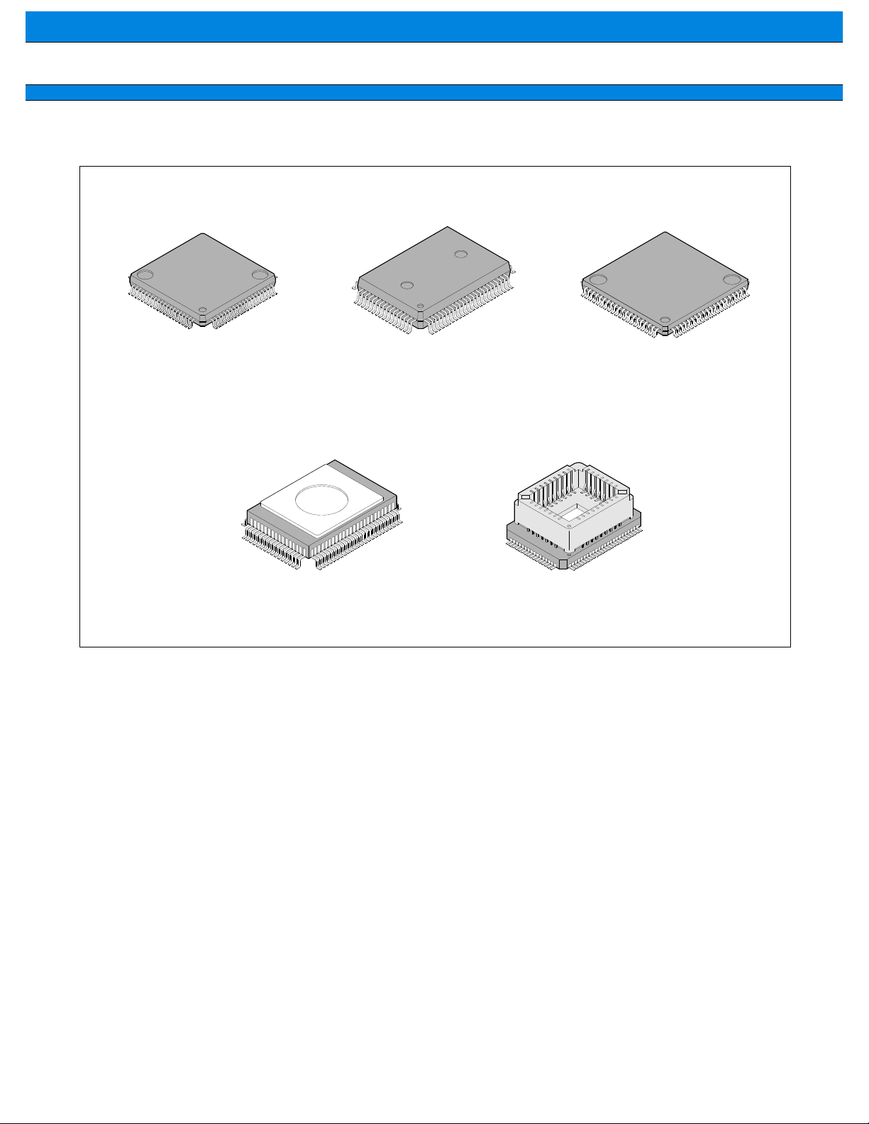
PACKAGE
80-pin Plastic SQFP
(FTP-80P-M05)
80-pin Ceramic QFP
80-pin Plastic QFP
(FTP-80P-M06)
80-pin Plastic QFP
(FTP-80P-M11)
80-pin Ceramic MQFP
(FTP-80C-A02)
(MQP-80C-P01)
2
■
To Top / Lineup / Index
MB89160/160A Series
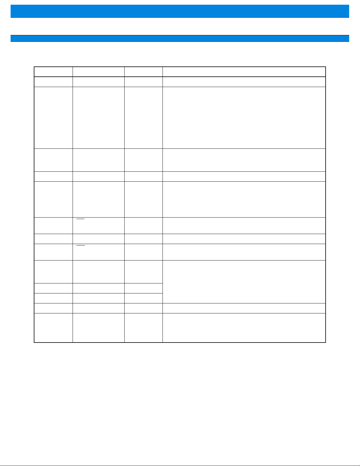
PRODUCT LINEUP
Part number
Parameter
Classification Mass production products
MB89161/
MB89161A
MB89163/
*1
MB89163A
*1
(mask ROM products)
MB89165/
MB89165A
MB89P165 MB89W165 MB89PV160
*1
One-time
PROM
product
EPROM
product
Piggyback/
evaluation
product (for
development)
ROM size 4 K × 8 bits
(internal mask
ROM)
8 K × 8 bits
(internal mask
ROM)
16 K × 8 bits
(internal mask
ROM)
16 K × 8 bits
(internal PROM, programming with
general-purpose EPROM
32 K × 8 bits
(external ROM)
programmer)
RAM size 128 × 8 bits 256 × 8 bits 512 × 8 bits
CPU functions Number of instructions: 136
Instruction bit length: 8 bits
Instruction length: 1 to 3 bytes
Data bit length: 1, 8,16 bits
Minimum execution time: 0.95 µ s/4.2 MHz
Interrupt processing time: 9 µ s/4.2 MHz
Ports I/O port (N-ch open-drain): 8 (6 ports also serve as peripherals, 3 ports
are a heavy-current drive type.)
Output ports (N-ch open-drain): 28 (16 ports also serve as segment pins, 2 ports
serve as booster capacitor connection pins,
2 ports serve as common pins.)
*3
(8 ports also serve as an A/D input)
I/O ports (CMOS): 16 (12 ports also serve as an external interrupt)
Output ports (CMOS): 2 (Also serve as peripherals)
Total: 54 (max.)
Timer/counter 8-bit timer operation (toggled output capable, operating clock cycle 1.9 µ s to 486 µ s)
16-bit timer operation (toggled output capable, operating clock cycle 1.9 µ s to 486 µ s)
Serial I/O 8 bits
LSB first/MSB first selectability
One clock selectable from four operation clocks
(one external shift clock, three internal shift clocks: 1.9 µ s, 7.6 µ s, 30.4 µ s)
LCD controller/driver
Common output: 4 (max.)
Segment output: 24 (max.)
*3
Bias power supply pins: 4
LCD display RAM size: 24 × 4 bits
Booster for LCD driving: Built-in (product with a booster)
Without a
booster for
*3
LCD driving
Dividing resistor for LCD driving: Built-in (an external resistor
selectability)
A/D converter 8-bit resolution × 8 channels
A/D conversion mode (conversion time 43 µ s/4.2 MHz (44 instruction cycles))
Sense mode (conversion time 11.9 µ s/4.2 MHz)
Continuous activation by an internal timer capable
Reference voltage input
(Continued)
3
■
To Top / Lineup / Index
MB89160/160A Series
(Continued)
Part number
Parameter
PWM timer 1,
PWM timer 2
External interrupt 1
(wake-up function)
External interrupt 2 “L” level interrupts × 8 channels
Buzzer output 1 (7 frequencies are selectable by the software.)
Remote control
transmission
output
Standby modes Subclock mode, sleep mode, stop mode, and watch mode
Process CMOS
Operating voltage
EPROM for use
MB89161/
MB89161A
MB89163/
*1
MB89163A
*1
MB89165A
MB89165/
MB89P165 MB89W165 MB89PV160
*1
8 bits × 2 channels
8-bit reload timer operation (toggled output capable, operating clock cycle: 0.95 µ s to
124 ms)
8-bit resolution PWM operation (conversion cycle: 243 µ s to 32 s)
4 independent channels (edge selectability)
Rising edge/falling edge selectability
Used also for wake-up from stop/sleep mode.
(Edge detection is also permitted in stop mode.)
1 (Pulse width and cycle are software selectable.)
*2
2.2 V to 6.0 V (single clock)/
2.2 V to 4.0 V (dual clock)
2.7 V to 6.0 V
MBM27C256A20TV
*1: Products with an internal booster.
*2: Varies with conditions such as the operating frequency. (The operating v oltage of the A/D con v erter is assured
separately. See section “ ■ Electrical Characteristics.”)
*3: See section “ ■ Mask Options.”
PACKAGE AND CORRESPONDING PRODUCTS
Package
MB89161
MB89161A
FPT-80P-M05
FPT-80P-M06
FPT-80P-M11
MQP-80C-P01
FPT-80C-A02
: Available
× : Not available
×××× Ч
ЧЧЧЧЧ
Note: For more information about each package, see section “ ■ Package Dimensions.”
MB89163
MB89163A
MB89165
MB89165A
MB89PW165 MB89W165 MB89PV160
××
××
××
4

■
To Top / Lineup / Index
MB89160/160A Series
DIFFERENCES AMONG PRODUCTS
1. Memory Size
Before evaluating using the piggyback product, verify its differences from the product that will actually be used.
Take particular care on the following points:
• On the MB89161/A and MB89163/A, the upper half of each register bank cannot be used.
• The stack area, etc., is set at the upper limit of the RAM.
2. Current Consumption
• In the case of the MB89PV160, add the current consumed by the EPROM which is connected to the top sock et.
• When operated at low speed, the product with an OTPROM (one-time PROM) or an EPROM will consume
more current than the product with a mask ROM.
However, the current consumption in the sleep/stop modes is the same. (For more information, see section
“ ■ Electrical Characteristics.”)
3. Mask Options
Functions that can be selected as options and how to designate these options vary by the product.
Before using options check section “ ■ Mask Options.”
Take particular care on the following points:
• A pull-up resistor cannot be set for P20 to P27 on the MB89P165.
• A pull-up resistor is not selectable for P40 to P47 and P60 to P67 if they are used as LCD pins.
• Options are fixed on the MB89PV160.
5

MB89160/160A Series
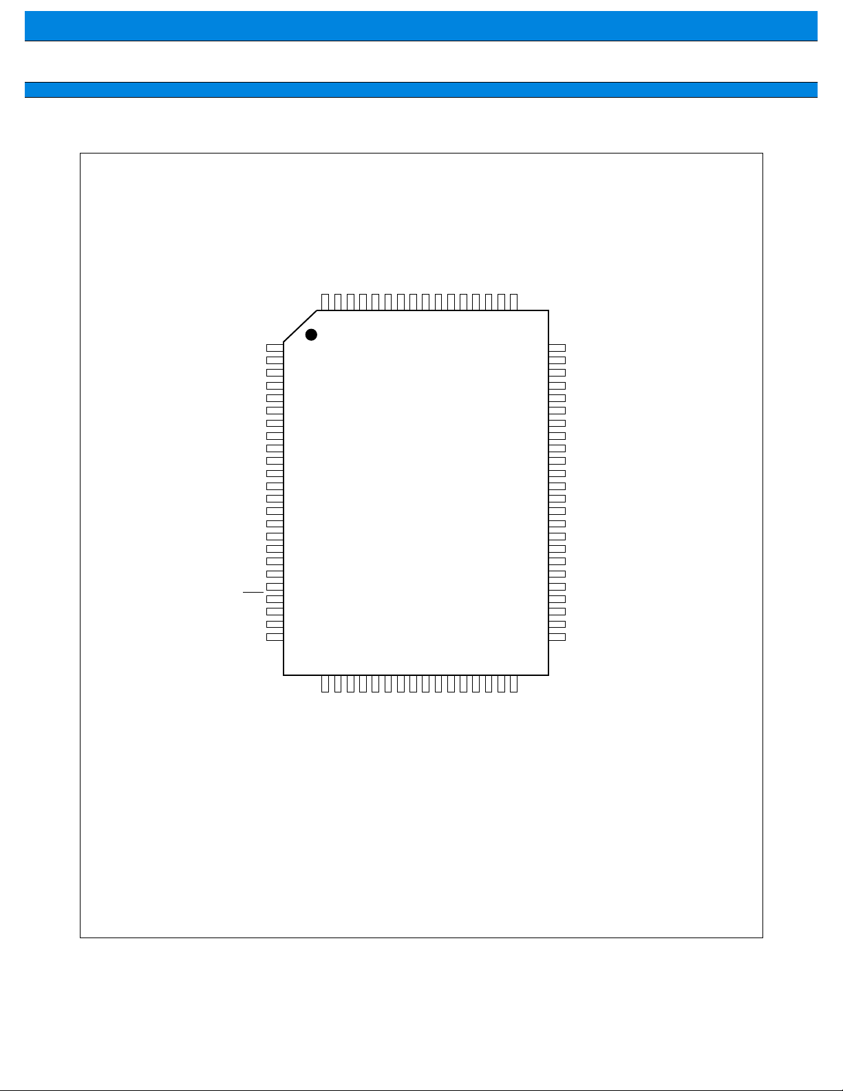
■
PIN ASSIGNMENT
7
7
6
6
6
P45/SEG21*
P44/SEG20*
P43/SEG19*
P42/SEG18*
P41/SEG17*
(Top view)
6
5
5
5
P40/SEG16*
P67/SEG15*
P66/SEG14*
P65/SEG13*
5
4
4
4
P64/SEG12*
P63/SEG11*
P62/SEG10*
P61/SEG9*
4
P60/SEG8*
SEG7
SEG6
SEG5
SEG4
SEG3
SEG2
To Top / Lineup / Index
P46/SEG22*
P47/SEG23*
AVSS
AVR
AV
P50/AN0
P51/AN1
P52/AN2
P53/AN3
P54/AN4
P55/AN5
P56/AN6
V
P57/AN7
MOD1
MOD0
RST
P00/INT20
X1
X0
80797877767574737271706968676665646362
7
1
7
2
3
4
CC
5
6
7
8
9
10
11
12
SS
13
14
15
16
17
18
19
20
21222324252627282930313233343536373839
3
P16
*
P17
P14
P15
P20/EC
P01/INT21
P02/INT22
P03/INT23
P04/INT24
P05/INT25
P06/INT26
P07/INT27
P10/INT10
P11/INT11
P12/INT12
P13/INT13
P21
P22/TO
61
40
P23/SI
P24/SO
60
59
58
57
56
55
54
53
52
51
50
49
48
47
46
45
44
43
42
41
SEG1
SEG0
P71/COM3*
P70/COM2*
8
8
COM1
COM0
V3
V
CC
V2
V1
V0
2
/C0*
1
1
P33*
P32*2/C1*
P31/PWM1
P30/RCO/BUZ
X1A
X0A
P27/PWM2*
P26*
3
3
P25/SCK
(FPT-80P-M11)
*1: For products with a booster circuit
*2: For products without a booster circuit
*3: N-ch open-drain heavy-current drive type
*4 to *7: Selected using the mask option (in units of 4 pins)
*8: Selected using the mask option (in units of 2 pins)
Note: For more information on mask option combinations of *4 to *8, see section “■ Mask Options.”
6
To Top / Lineup / Index
MB89160/160A Series
(Top view)
6
6
6
6
5
5
5
5
4
4
4
4
P43/SEG19*
P42/SEG18*
P41/SEG17*
P40/SEG16*
P67/SEG15*
P66/SEG14*
P65/SEG13*
P64/SEG12*
P63/SEG11*
P62/SEG10*
P61/SEG9*
P60/SEG8*
SEG7
SEG6
SEG5
SEG4
P44/SEG20*
P45/SEG21*
P46/SEG22*
P47/SEG23*
AVSS
AVR
AV
P50/AN0
P51/AN1
P52/AN2
P53/AN3
P54/AN4
P55/AN5
P56/AN6
V
P57/AN7
MOD1
MOD0
RST
P00/INT20
P01/INT21
P02/INT22
X1
X0
807978777675747372717069686766
7
1
7
2
7
3
7
4
5
6
CC
7
8
9
10
11
12
13
14
SS
15
16
17
18
19
20
21
22
23
24
252627282930313233343536373839
P14
P15
P16
P03/INT23
P04/INT24
P05/INT25
P06/INT26
P07/INT27
P10/INT10
P11/INT11
P12/INT12
P13/INT13
P17
P20/EC
3
P21*
65
64
63
62
61
60
59
58
57
56
55
54
53
52
51
50
49
48
47
46
45
44
43
42
41
40
P22/TO
SEG3
SEG2
SEG1
SEG0
P71/COM3*
P70/COM2*
8
8
COM1
COM0
V3
V
CC
V2
V1
V0
2
/C0*
1
1
P33*
P32*2/C1*
P31/PWM1
P30/RCO/BUZ
X1A
X0A
P27/PWM2*
P26*
3
3
P25/SCK
P24/SO
P23/SI
(FPT-80P-M06)
(FPT-80C-A02)
*1: For products with a booster circuit
*2: For products without a booster circuit
*3: N-ch open-drain heavy-current drive type
*4 to *7: Selected using the mask option (in units of 4 pins)
*8: Selected using the mask option (in units of 2 pins)
Note: For more information on mask option combinations of *4 to *8, see section “■ Mask Options.”
7
MB89160/160A Series
7
7
6
6
6
P45/SEG21*
P44/SEG20*
P43/SEG19*
P42/SEG18*
P41/SEG17*
(Top view)
6
5
5
5
P40/SEG16*
P67/SEG15*
P66/SEG14*
P65/SEG13*
5
4
4
4
P64/SEG12*
P63/SEG11*
P62/SEG10*
P61/SEG9*
4
P60/SEG8*
SEG7
SEG6
SEG5
SEG4
SEG3
To Top / Lineup / Index
SEG2
P46/SEG22*
P47/SEG23*
AVSS
AVR
AV
P50/AN0
P51/AN1
P52/AN2
P53/AN3
P54/AN4
P55/AN5
P56/AN6
V
P57/AN7
MOD1
MOD0
RST
P00/INT20
X1
X0
80797877767574737271706968676665646362
7
1
7
2
3
4
CC
5
6
7
8
9
10
11
12
SS
13
14
15
16
17
18
19
20
21222324252627282930313233343536373839
3
P14
P15
P16
P17
P20/EC
P01/INT21
P02/INT22
P03/INT23
P04/INT24
P05/INT25
P06/INT26
P07/INT27
P10/INT10
P11/INT11
P12/INT12
P13/INT13
P21*
P22/TO
61
40
P23/SI
P24/SO
60
59
58
57
56
55
54
53
52
51
50
49
48
47
46
45
44
43
42
41
SEG1
SEG0
P71/COM3*
P70/COM2*
8
8
COM1
COM0
V3
V
CC
V2
V1
V0
2
/C0*
1
1
P33*
P32*2/C1*
P31/PWM1
P30/RCO/BUZ
X1A
X0A
P27/PWM2*
P26*
3
3
P25/SCK
(FPT-80P-M05)
*1: For products with a booster circuit
*2: For products without a booster circuit
*3: N-ch open-drain heavy-current drive type
*4 to *7: Selected using the mask option (in units of 4 pins)
*8: Selected using the mask option (in units of 2 pins)
Note: For more information on mask option combinations of *4 to *8, see section “■ Mask Options.”
8
•
To Top / Lineup / Index
MB89160/160A Series
(Top view)
6
6
6
6
5
5
5
5
4
4
4
4
P43/SEG19*
P42/SEG18*
P41/SEG17*
P40/SEG16*
P67/SEG15*
P66/SEG14*
P65/SEG13*
P64/SEG12*
P63/SEG11*
P62/SEG10*
P61/SEG9*
P60/SEG8*
SEG7
SEG6
SEG5
SEG4
P44/SEG20*
P45/SEG21*
P46/SEG22*
P47/SEG23*
AV
AVR
AV
P50/AN0
P51/AN1
P52/AN2
P53/AN3
P54/AN4
P55/AN5
P56/AN6
V
P57/AN7
X1
X0
MOD1
MOD0
RST
P00/INT20
P01/INT21
P02/INT22
807978777675747372717069686766
7
1
7
2
7
3
7
4
SS
5
6
CC
7
8
9
10
11
12
13
14
SS
15
16
17
18
19
20
100999897969594
101
102
103
104
105
106
107
108
109
818283
110
111
112
93
92
91
90
89
88
87
86
85
84
21
22
23
24
252627282930313233343536373839
P14
P15
P16
P03/INT23
P04/INT24
P05/INT25
P06/INT26
P07/INT27
P10/INT10
P11/INT11
P12/INT12
P13/INT13
P17
3
P21*
P20/EC
65
64
63
62
61
60
59
58
57
56
55
54
53
52
51
50
49
48
47
46
45
44
43
42
41
40
P22/TO
SEG3
SEG2
SEG1
SEG0
P71/COM3*
P70/COM2*
8
8
COM1
COM0
V3
V
CC
V2
V1
V0
2
/C0*
1
1
P33*
P32*2/C1*
P31/PWM1
P30/RCO/BUZ
X1A
X0A
P27/PWM2*
P26*
3
3
P25/SCK
P24/SO
P23/SI
(MQP-80C-P01)
*1: For products with a booster circuit
*2: For products without a booster circuit
*3: N-ch open-drain heavy-current drive type
*4 to *7: Selected using the mask option (in units of 4 pins)
*8: Selected using the mask option (in units of 2 pins)
Note: For more information on mask option combinations of *4 to *8, see section “■ Mask Options.”
Pin assignment on package top (MB89PV160 only)
Pin no. Pin name Pin no. Pin name Pin no. Pin name Pin no. Pin name
81 N.C. 89 A2 97 N.C. 105 OE
82 V
PP
90 A1 98 O4 106 N.C.
83 A12 91 A0 99 O5 107 A11
84 A7 92 N.C. 100 O6 108 A9
85 A6 93 O1 101 O7 109 A8
86 A5 94 O2 102 O8 110 A13
87 A4 95 O3 103 CE
88 A3 96 V
SS
104 A10 112 V
111 A14
CC
N.C.: Internally connected. Do not use.
9
MB89160/160A Series
■
PIN DESCRIPTION
To Top / Lineup / Index
SQFP
QFP
Pin no.
*1
*2
MQFP
QFP
*3
*4
Pin name
Circuit
type
Function
16 18 X0 A Main clock crystal oscillator pins
15 17 X1
CR oscillation selectability (mask products only)
18 20 MOD0 C Operating mode selection pins
17 19 MOD1
19 21 RST
Connect directly to V
D Reset I/O pin
SS
.
This pin is an N-ch open-drain output type with a
pull-up resistor, and a hysteresis input type. “L” is
output from this pin by an internal reset source. The
internal circuit is initialized by the input of “L”.
20 to 27 22 to 29 P00/INT20 to
P07/INT27
E General-purpose I/O ports
Also serve as an external interrupt 2 input (wake-up
function).
External interrupt 2 input is hysteresis input.
28 to 31 30 to 33 P10/INT10 to
P13/INT13
E General-purpose I/O ports
Also serve as an external interrupt 1 input. External
interrupt 1 input is hysteresis input.
32 to 35 34 to 37 P14 to P17 F General-purpose I/O ports
36 38 P20/EC H N-ch open-drain general-purpose I/O port
Also serves as the external clock input for the timer.
The peripheral is a hysteresis input type.
37 39 P21 I N-ch open-drain general-purpose I/O port
38 40 P22/TO I N-ch open-drain general-purpose I/O port
Also serves as a timer output.
39 41 P23/SI H N-ch open-drain general-purpose I/O port
Also serves as the data input for the serial I/O. The
peripheral is a hysteresis input type.
40 42 P24/SO I N-ch open-drain general-purpose I/O port
Also serves as the data output for the serial I/O.
41 43 P25/SCK H N-ch open-drain general-purpose I/O port
Also serves as the clock I/O for the serial I/O. The
peripheral is a hysteresis input type.
42 44 P26 I N-ch open-drain general-purpose I/O port
43 45 P27/PWM2 I N-ch open-drain general-purpose I/O port
Also serves as the square wave or PWM wave
output for the 8-bit PWM timer 2.
49 51 P33 J Functions as an N-ch open-drain general-purpose
output port only in the products without a booster.
C0 — Functions as a capacitor connection pin in the
products with a booster.
*1: FPT-80P-M05
*2: FPT-80P-M11
*3: MQP-80C-P01
*4: FPT-80P-M06
10
(Continued)
To Top / Lineup / Index
MB89160/160A Series
(Continued)
SQFP
QFP
Pin no.
*1
*2
MQFP
QFP
*3
*4
Pin name
Circuit
type
Function
48 50 P32 J Functions as an N-ch open-drain general-purpose
output port only in the products without a booster.
C1 — Functions as a capacitor connection pin in the
products with a booster.
47 49 P31/PWM1 G General-purpose output-only port
Also serves as the square wave or PWM wave
output for the 8-bit PWM timer 1.
46 48 P30/RCO/BUZ G General-purpose output-only port
Also serves as a buzzer output and a remote
control transmission frequency output.
14,
12 to 6
2, 1,
80 to 75
74 to 67 76 to 69 P67/SEG15 to
16,
14 to 8
4 to 1
80 to 77
P57/AN7 to
P50/AN0
P47/SEG23 to
P40/SEG16
P60/SEG8
L N-ch open-drain general-purpose output ports
Also serve as an analog input.
J/K N-ch open-drain general-purpose output ports
Also serve as an LCD controller/driver segment
J/K
output. Switching between port and segment output
is done by the mask option.
66 to 59 68 to 61 SEG7 to SEG0 K LCD controller/driver segment output pins
58,
57
60,
59
P71/COM3,
P70/COM2
J/K N-ch open-drain general-purpose output ports
Also serve as an LCD controller/driver common
output. Switching between port and common output
is done by the mask option.
56,
55
54,
52 to 50
58,
57
56,
54 to 52
COM1,
COM0
V3,
V2 to V0
K LCD controller/driver common output-only pins
— LCD driving power supply pins
44 46 X0A B Subclock crystal oscillator pins (32.768 KHz)
45 47 X1A
53 55 V
13 15 V
57AV
CC
SS
SS
— Power supply pin
— Power supply (GND) pin
— A/D converter power supply pin
Use this pin at the same voltage as V
CC
.
4 6 AVR — A/D converter reference voltage input pin
35AV
SS
— A/D converter power supply pin
Use this pin at the same voltage as V
SS
.
*1: FPT-80P-M05
*2: FPT-80P-M11
*3: MQP-80C-P01
*4: FPT-80P-M06
11
•
MB89160/160A Series
External EPROM pins (MB89PV160 only)
Pin no. Pin name I/O Function
82 V
83
84
85
86
87
88
89
90
91
93
94
95
96 V
98
99
100
101
102
103 CE
104 A10 O Address output pin
105 OE O ROM output enable pin
107
108
109
110 A13 O
111 A14 O
112 V
81
92
97
106
PP
A12
A7
A6
A5
A4
A3
A2
A1
A0
O1
O2
O3
SS
O4
O5
O6
O7
O8
A11
A9
A8
CC
N.C. — Internally connected pins
O “H” level output pin
O Address output pins
I Data input pins
O Power supply (GND) pin
I Data input pins
O ROM chip enable pin
Outputs “H” during standby.
Outputs “L” at all times.
O Address output pins
O EPROM power supply pin
Be sure to leave them open.
To Top / Lineup / Index
12
■
To Top / Lineup / Index
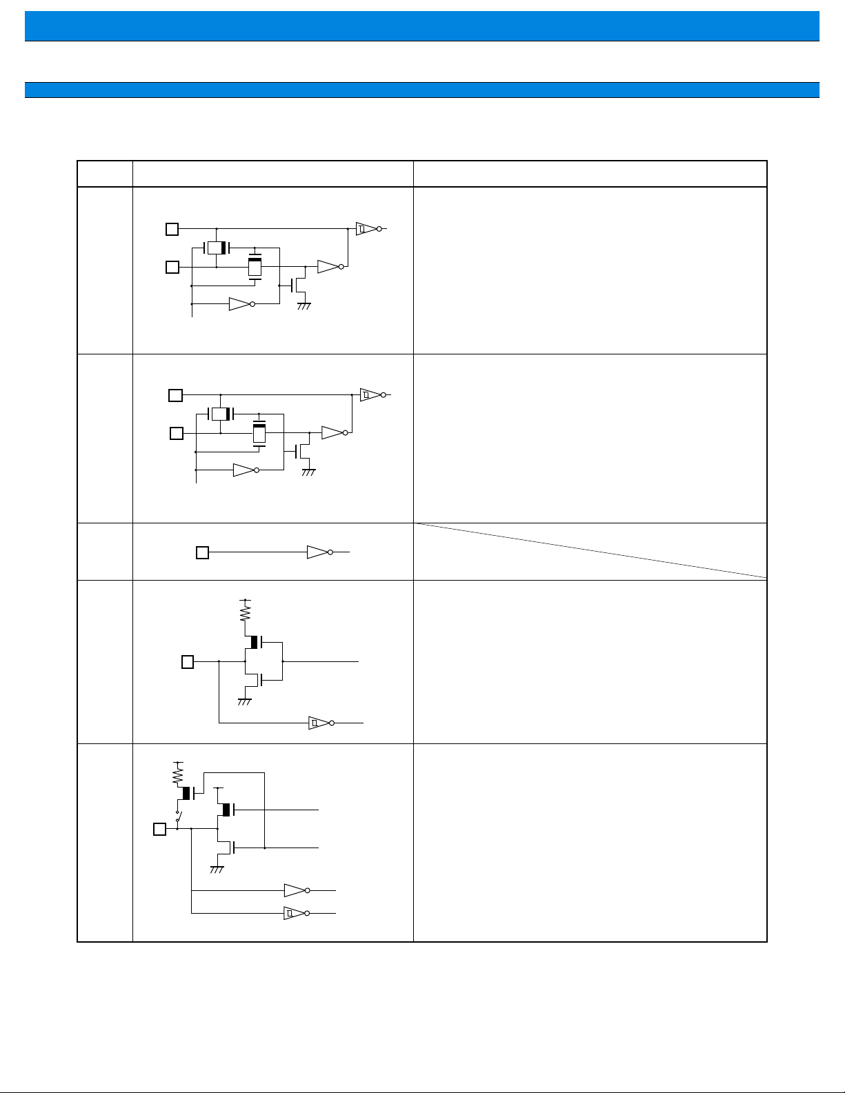
MB89160/160A Series
I/O CIRCUIT TYPE
Type Circuit Remarks
A Main clock
X1
X0
Standby control signal
B Subclock
X1A
X0A
• At an oscillation feedback resistor of approximately
1 M Ω /5.0 V
• CR oscillation is selectable (MB8916X/A only).
• At an oscillation feedback resistor of approximately
4.5 M Ω /5.0 V
Standby control signal
C
D • At an output pull-up resistor of approximately
R
P-ch
N-ch
50 k Ω /5.0 V
• Hysteresis input
E • CMOS I/O
P-ch
R
P-ch
N-ch
Port
Peripheral
• The peripheral is a hysteresis input type.
• Pull-up resistor optional
(Not available on the MB89PV160.)
(Continued)
13
MB89160/160A Series
To Top / Lineup / Index
(Continued)
Type Circuit Remarks
F • CMOS I/O
R
P-ch
P-ch
N-ch
• Pull-up resistor optional
(Not available on the MB89PV160)
G • CMOS output
P-ch
N-ch
Port
• P-ch output is a heavy-current drive type.
H • N-ch open-drain I/O
R
P-ch
• CMOS input
• The peripheral is a hysteresis input type.
• P21, P26, and P27 are a heavy-current drive type.
• Pull-up resistor optional
(Not available on the MB89P165/A, MB89W165/A
N-ch
and MB89PV160)
Port
Peripheral
I • N-ch open-drain output
P-ch
R
N-ch
• CMOS input
• Pull-up resistor optional
Port
(Not available on the MB89P165/A, MB89W165/A
and MB89PV160)
J • N-ch open-drain output
R
P-ch
• Pull-up resistor optional
(Not available on the MB89P165/A, MB89W165/A
and MB89PV160)
• P32 and P33 are not provided with a pull-up resistor.
N-ch
(Continued)
14
To Top / Lineup / Index
MB89160/160A Series
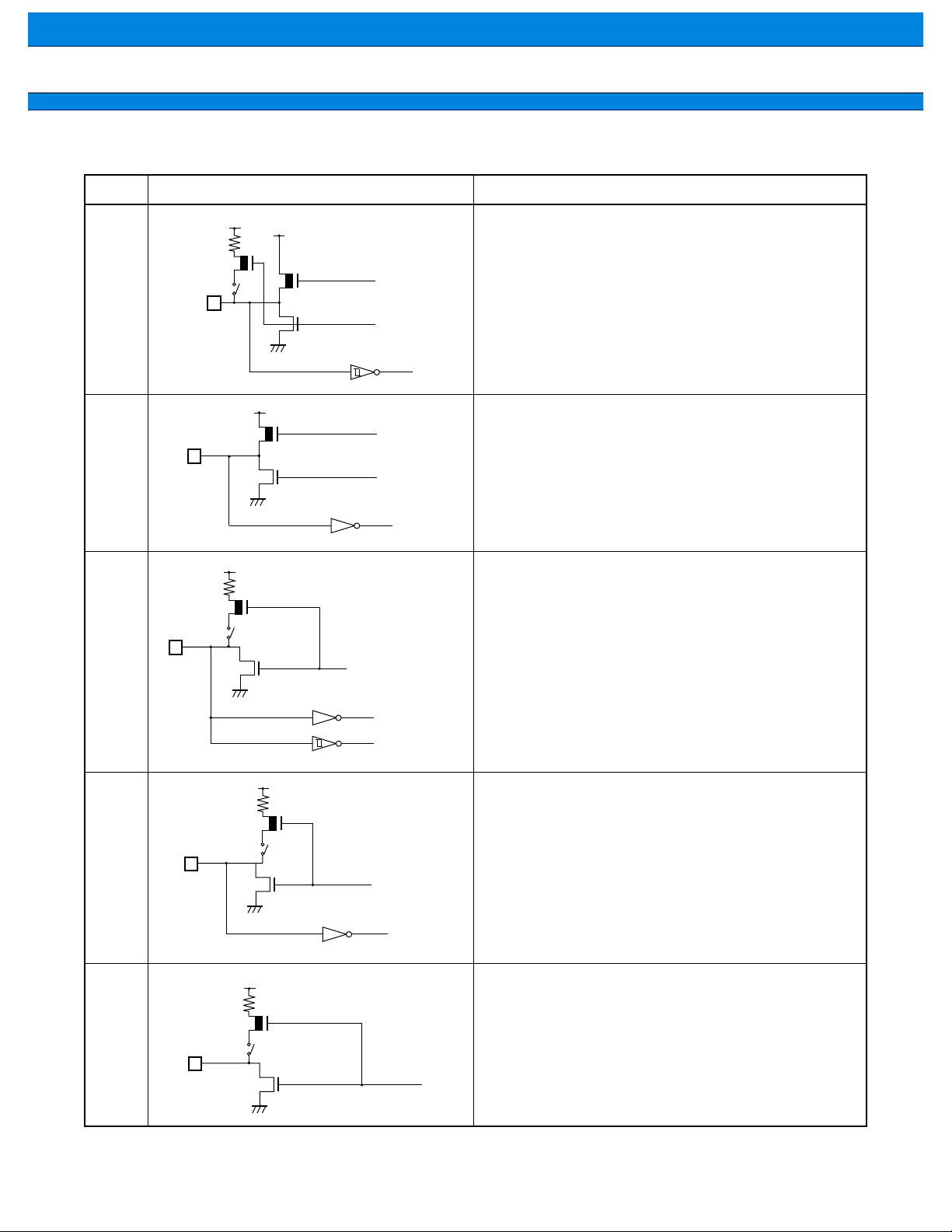
(Continued)
Type Circuit Remarks
K • LCD controller/driver segment output
P-ch
N-ch
P-ch
N-ch
L • N-ch open-drain output
P-ch
R
P-ch
• Analog input
N-ch
Analog input
• Pull-up resistor optional
(Not available on the MB89PV160)
15

■
MB89160/160A Series
HANDLING DEVICES
1. Preventing Latchup
To Top / Lineup / Index
Latchup may occur on CMOS ICs if voltage higher than V
or lower than V
CC
is applied to input and output pins
SS
other than medium- to high-voltage pins or if higher than the voltage which shows on “ 1. Absolute Maximum
Ratings” in section “ ■ Electrical Characteristics” is applied between V
CC
to V
SS
.
When latchup occurs, power supply current increases rapidly and might thermally damage elements. When
using, take great care not to exceed the absolute maximum ratings.
Also, take care to pre v ent the analog po wer supply (AV
power supply (V
) when the analog system power supply is turned on and off.
CC
and A VR) and analog input from e xceeding the digital
CC
2. Treatment of Unused Input Pins
Leaving unused input pins open could cause malfunctions. They should be connected to a pull-up or pull-down
resistor.
3. Treatment of Power Supply Pins on Microcontrollers with A/D and D/A Converters
Connect to be AV
CC
= DAVC = V
CC
and AV
SS
= AVR = V
SS
even if the A/D and D/A converters are not in use.
4. Treatment of N.C. Pin
Be sure to leave (internally connected) N.C. pins open.
5. Power Supply Voltage Fluctuations
Although V
could cause malfunctions, even if it occurs within the rated range. Stabilizing voltage supplied to the IC is
therefore important. As stabilization guidelines, it is recommended to control power so that V
(P-P value) will be less than 10% of the standard V
transient fluctuation rate will be less than 0.1 V/ms at the time of a momentary fluctuation such as when power
is switched.
CC
power supply voltage is assured to operate within the rated range, a rapid fluctuation of the voltage
ripple fluctuations
CC
CC
value at the commercial frequency (50 to 60 Hz) and the
6. Precautions when Using an External Clock
Even when an external clock is used, oscillation stabilization time is required for power-on reset (optional) and
wake-up from stop mode.
16
■
To Top / Lineup / Index
MB89160/160A Series
PROGRAMMING T O THE EPROM ON THE MB89P165
The MB89P165 is an OTPROM version of the MB89160 series.
1. Features
• 32-Kbyte PROM on chip
• Options can be set using the EPROM programmer.
• Equivalency to the MBM27C256A in EPROM mode (when programmed with the EPROM programmer)
2. Memory Space
Memory space in each mode such as 32-Kbyte PROM, option area is diagrammed below.
Address
0000H
H
0080
0280H
8000H
C000H 4000H
FFFFH
Single-chip EPROM mode
I/O
RAM
Not available
Not available
Not available
PROM
16 KB
(Corresponding addresses on the EPROM programmer)
0000
3FF0
3FF6H
7FFFH
H
H
Not available
Option areaNot available
Not available
EPROM
16 KB
3. Programming to the EPROM
In EPROM mode, the MB89P165 functions equivalent to the MBM27C256A. This allows the PROM to be
programmed with a general-purpose EPROM programmer (the electronic signature mode cannot be used) by
using the dedicated socket adapter.
When the operating area for a single chip is 16 Kbyte (C000
H
to FFFF
• Programming procedure
(1) Set the EPROM programmer to the MBM27C256A.
(2) Load program into the EPROM programmer at 4000
(Note that addresses C000
H
to FFFF
H
while operating as a single chip assign to 4000
H
to 7FFF
mode.)
Load option data into address 3FF0
H
to 3FF5
H
of the EPROM programmer.
(For information about each corresponding option, see “8. Setting OTPROM Options.”)
(3) Program with the EPROM programmer.
H
) the PROM can be programmed as f ollows:
H
.
H
to 7FFF
H
in EPROM
17
To Top / Lineup / Index
MB89160/160A Series
4. Recommended Screening Conditions
High-temperature aging is recommended as the pre-assembly screening procedure for a product with a blanked
OTPROM microcomputer program.
Program, verify
Aging
+150°C, 48 Hrs.
Data verification
Assembly
5. Programming Yield
All bits cannot be programmed at Fujitsu shipping test to a blanked OTPROM microcomputer, due to its nature.
For this reason, a programming yield of 100% cannot be assured at all times.
6. EPROM Programmer Adapter Socket
Package Compatible adapter socket
FPT-80P-M05 ROM-80SQF-28DP-8L
FPT-80P-M06 ROM-80QF-28DP-8L3
FPT-80P-M11 ROM-80QF2-28DP-8L2
7. Erasure
In order to clear all locations of their programmed contents, it is necessary to expose the internal EPROM to an
ultraviolet light source. A dosage of 10 W -seconds/cm
dosage can be obtained by exposure to an ultraviolet lamp (wavelength of 2537 Angstroms (Å)) with intensity
of 12000 µ W/cm
filters should be removed from the UV light source prior to erasure.
It is important to note that the internal EPROM and similar devices, will erase with light sources having
wavelengths shorter than 4000Å. Although erasure time will be much longer than with UV source at 2537Å,
nevertheless the exposure to fluorescent light and sunlight will eventually erase the internal EPROM, and
exposure to them should be prevented to realize maximum system reliability. If used in such an environment,
the package windows should be covered by an opaque label or substance.
18
for 15 to 21 minutes. The internal EPROM should be about one inch from the source and all
2
2
is required to completely erase an internal EPROM. This

•
To Top / Lineup / Index
MB89160/160A Series
8. Setting OTPROM Options
The programming procedure is the same as that for the PROM. Options can be set by programming value at
the addresses shown on the memory map. The relationship between bits and options is shown on the following
bit map:
OTPROM option bit map
Bit 7 Bit 6 Bit 5 Bit 4 Bit 3 Bit 2 Bit 1 Bit 0
3FF0
3FF1
3FF2
3FF3
3FF4
3FF5
Vacancy
H
Readable
P07
Pull-up
H
1: No
0: Yes
P17
Pull-up
H
1: No
0: Yes
P57
Pull-up
H
1: No
0: Yes
V acancy
H
Readable
V acancy
H
Readable
Vacancy
Readable
P06
Pull-up
1: No
0: Yes
P16
Pull-up
1: No
0: Yes
P56
Pull-up
1: No
0: Yes
V acancy
Readable
V acancy
Readable
Oscillation stabilization time
WTM1 WTM0
See section “ ■ Mask Option.”
P05
Pull-up
1: No
0: Yes
P15
Pull-up
1: No
0: Yes
P55
Pull-up
1: No
0: Yes
V acancy
Readable
V acancy
Readable
P04
Pull-up
1: No
0: Yes
P14
Pull-up
1: No
0: Yes
P54
Pull-up
1: No
0: Yes
V acancy
Readable
V acancy
Readable
Vacancy
Readable
P03
Pull-up
1: No
0: Yes
P13
Pull-up
1: No
0: Yes
P53
Pull-up
1: No
0: Yes
V acancy
Readable
V acancy
Readable
Reset pin
output
1: Yes
0: No
P02
Pull-up
1: No
0: Yes
P12
Pull-up
1: No
0: Yes
P52
Pull-up
1: No
0: Yes
V acancy
Readable
V acancy
Readable
Clock mode
selection
1: Dual clock
0: Single
clock
P01
Pull-up
1: No
0: Yes
P11
Pull-up
1: No
0: Yes
P51
Pull-up
1: No
0: Yes
V acancy
Readable
V acancy
Readable
Power-on
reset
1: Yes
0: No
P00
Pull-up
1: No
0: Yes
P10
Pull-up
1: No
0: Yes
P50
Pull-up
1: No
0: Yes
V acancy
Readable
V acancy
Readable
Notes: • Set each bit to 1 to erase.
• Do not write 0 to the vacant bit.
The read value of the vacant bit is 1, unless 0 is written to it.
19

■
To Top / Lineup / Index
MB89160/160A Series
PROGRAMMING TO THE EPROM WITH PIGGYBACK/EVALUATION DEVICE
1. EPROM for Use
MBM27C256A-20TV
2. Programming Socket Adapter
To program to the PROM using an EPROM programmer, use the socket adapter (manufacturer: Sun Hayato
Co., Ltd.) listed below.
Package Adapter socket part number
LCC-32 (Rectangle) ROM-32LC-28DP-YG
Inquiry: Sun Hayato Co., Ltd.: TEL 81-3-3802-5760
3. Memory Space
Memory space in each mode, such as 32-Kbyte PROM, option area is diagrammed below.
Address
0000
H
0080H
H
0280
8000H 0000H
FFFFH
Single chip
I/O
RAM
Not available
PROM
32 KB
Corresponding addresses on the EPROM programmer
EPROM
32 KB
7FFFH
4. Programming to the EPROM
(1) Set the EPROM programmer to the MBM27C256A.
(2) Load program data into the EPROM programmer at 0000
(3) Program to 0000H to 7FFFH with the EPROM programmer.
20
H to 7FFFH.

■
To Top / Lineup / Index
MB89160/160A Series
BLOCK DIAGRAM
X0
X1
X0A
X1A
RST
P00/INT20
to P07/INT27
P10/INT10
to P13/INT13
P14 to P17
P50/AN0
to P57/AN7
AVCC
AVR
AVSS
Clock controller
Subclock oscillator
(32.768 KHz)
Watch prescaler timer
Reset circuit
8
4
4
8 8
8
External interrupt 2
(Wake-up)
Port 0
CMOS I/O port
4
External interrupt 1
Port 1
CMOS I/O port
RAM
F2MC-8L
CPU
ROM
N-ch open-drain output port
8-bit A/D converter
Port 5
Main clock
oscillator
(WDT)
(Wake-up)
Time-base timer
8-bit timer/counter
8-bit timer/counter
Internal bus
8-bit PWM timer 2
8-bit serial
N-ch open-drain I/O port
N-ch open-drain output port
LCD
controller/driver
24 × 4 bits
Reference voltage
generator and booster*
8-bit PWM timer 1
Remote control output
VRAM
8 4
8
2
1
P22/TO
P20/EC
Port 2
P27/PWM2*
P25/SCK
P24/SO
P23/SI
4
P21*
, P26*
4
P40/SEG16*
to P43/SEG19
P44/SEG20*
to P47/SEG23
Port 4Port 6 and port 7
4
P60/SEG8*
to P63/SEG11
4
P64/SEG12*
to P67/SEG15
2
P70/COM2*
P71/COM3
8
SEG0 to SEG7
2
COM0, COM1
4
V0 to V3
P33/C0*
P32/C1*
P31/PWM1
P30/RCO/BUZ
4
4
3
3
3
3
3
,
2
2
Other pins
MOD0, MOD1, V
*1: Selected by mask option
*2: Used as ports without a reference voltage generator and booster
*3: Functions selected by mask option. (For information on selecting procedure, see section “■ Mask Options.”)
*4: Heavy-current drive type
CC, VSS
Buzzer output
N-ch open-drain I/O port
(P30 and P31 are a CMOS
output type.)
21

■
MB89160/160A Series
CPU CORE
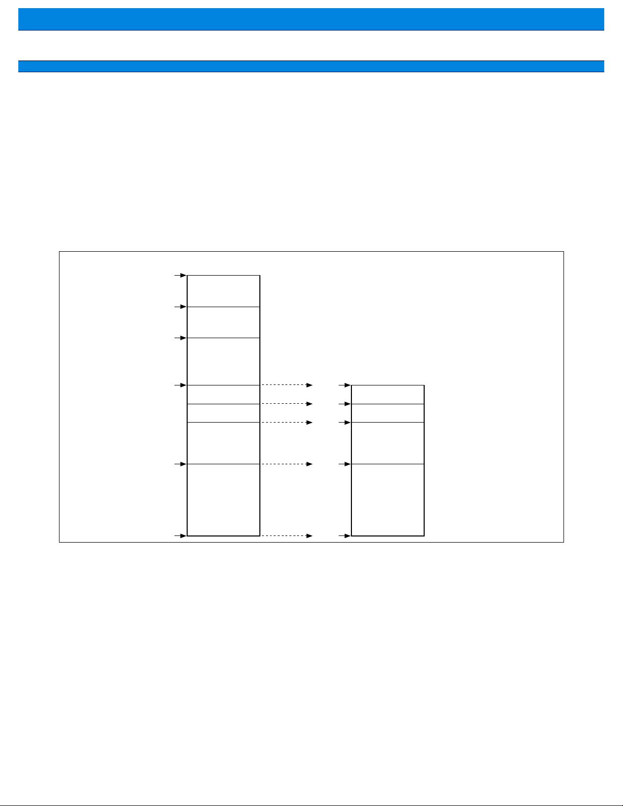
1. Memory Space
The microcontrollers of the MB89160 series offer a memory space of 64 Kbytes for storing all of I/O, data, and
program areas. The I/O area is located at the lowest address. The data area is provided immediately above the
I/O area. The data area can be divided into register, stack, and direct areas according to the application. The
program area is located at exactly the opposite end, that is, near the highest address. Provide the tables of
interrupt reset vectors and vector call instructions toward the highest address within the program area. The
memory space of the MB89160 series is structured as illustrated below.
Memory Space
To Top / Lineup / Index
0000
0080H
0100H
0200H
0280H
8000H
FFFFH
MB89PV160 MB89161/A MB89163/A
H
I/O
RAM
256 B
Register
Not available
External ROM
32 KB
0000
0080H
00C0H
0100H
0140H
F000H
FFFFH
H
I/O
Not available
RAM
128 B
Register
Not available
ROM
4 KB
0000
0080H
0100H
0180H
E000H
FFFFH
H
Not available
I/O
RAM
256 B
ROM
8 KB
Register
0000
0080H
0100H
0200H
0280H
C000H
FFFFH
MB89165/A
MB89P165
H
RAM
512 B
Not available
ROM
16 KB
I/O
Register
22

To Top / Lineup / Index
MB89160/160A Series
2. Registers
2
The F
MC-8L family has two types of registers; dedicated registers in the CPU and general-purpose registers
in the memory. The following dedicated registers are provided:
Program counter (PC): A 16-bit register for indicating instruction storage positions
Accumulator (A): A 16-bit temporary register for storing arithmetic operations, etc. When the
instruction is an 8-bit data processing instruction, the lower byte is used.
Temporary accumulator (T): A 16-bit register which performs arithmetic operations with the accumulator
When the instruction is an 18-bit data processing instruction, the lower byte is used.
Index register (IX): A 16-bit register for index modification
Extra pointer (EP): A 16-bit pointer for indicating a memory address
Stack pointer (SP): A 16-bit register for indicating a stack area
Program status (PS): A 16-bit register for storing a register pointer, a condition code
16 bits
PC
A
T
IX
EP
SP
PS
: Program counter
: Accumulator
: Temporary accumulator
: Index register
: Extra pointer
: Stack pointer
: Program status
Initial value
FFFD
H
Undefined
Undefined
Undefined
Undefined
Undefined
I-flag = 0, IL1, 0 = 11
Other bits are undefined.
The PS can further be divide into higher 8 bits for use as a register bank pointer (RP) and the lower 8 bits for
use as a condition code register (CCR). (See the diagram below.)
Structure of the Program Status Register
109876 321015 14 13 12 11
Vacancy
RPPS
RP CCR
Vacancy
H I IL1, 0 N Z VC
Vacancy
54
23

To Top / Lineup / Index
MB89160/160A Series
The RP indicates the address of the register bank currently in use. The relationship between the pointer contents
and the actual address is based on the conversion rule illustrated below.
Rule for Conversion of Actual Addresses of the General-purpose Register Area
Lower OP codesRP
“0”
“0”
“0”
“0”
“0”
“0”
“0”
“1”
R4
R3
R2
R1
R0
b2
b1
b0
↓
↓
↓
↓
↓
↓
↓
↓
↓
↓
↓
↓
↓
↓
↓
↓
A15
A14
A13
A12
A11
A10
A9
A8
A7
A6
A5
A4
A3
A2
A1
Generated addresses
The CCR consists of bits indicating the results of arithmetic operations and the contents of transfer data and
bits for control of CPU operations at the time of an interrupt.
A0
H-flag: Set when a carry or a borrow from bit 3 to bit 4 occurs as a result of an arithmetic operation. Cleared
otherwise. This flag is for decimal adjustment instructions.
I-flag: Interrupt is allowed when this flag is set to 1. Interrupt is prohibited when the flag is set to 0. Set to 0
when reset.
IL1, 0: Indicates the level of the interrupt currently allowed. Processes an interrupt only if its request level is
higher than the value indicated by this bit.
IL1 IL0 Interrupt level High-low
00
1
01
10 2
11 3
N-flag: Set if the MSB is set to 1 as the result of an arithmetic operation. Cleared when the bit is set to 0.
Z-flag: Set when an arithmetic operation results in 0. Cleared otherwise.
V -flag: Set if the complement on 2 ov erflo ws as a result of an arithmetic operation. Reset if the overflow does
not occur.
C-flag: Set when a carry or a borrow from bit 7 occurs as a result of an arithmetic operation. Cleared otherwise.
Set the shift-out value in the case of a shift instruction.
High
Low = no interrupt
24

To Top / Lineup / Index
MB89160/160A Series
The following general-purpose registers are provided:
General-purpose registers: An 8-bit register for storing data
The general-purpose registers are 8 bits and located in the register banks of the memory. One bank contains
eight registers. Up to a total of 16 banks can be used on the MB89163 (RAM 256 × 8 bits), and a total of 32
banks can be used on the MB89165 (RAM 256 × 8 bits). The bank currently in use is indicated by the register
bank pointer (RP).
Note: The number of register banks that can be used varies with the RAM size.
Register Bank Configuraiton
This address = 0100H + 8 × (RP)
R 0
R 1
R 2
R 3
R 4
R 5
R 6
R 7
Memory area
16 banks (MB89163)
32 banks (MB89165)
25

■
MB89160/160A Series
I/O MAP
Address Read/write Register name Register description
00
H
01
H
02
H
03
H
04
H
05
H
06
H
07
H
08
H
09
H
0A
H
0B
H
0C
H
0D
H
0E
H
0F
H
10
(R/W) BUZR Buzzer register
H
11
H
12
H
13
H
14
H
15
H
16
H
17
H
18
H
19
H
1A
H
1B
H
1C
H
1D
H
1E
H
1F
H
(R/W) PDR0 Port 0 data register
(W) DDR0 Port 0 data direction register
(R/W) PDR1 Port 1 data register
(W) DDR1 Port 1 data direction register
(R/W) PDR2 Port 2 data register
(W) DDR2 Port 2 data direction register
Vacancy
(R/W) SYCC System clock control register
(R/W) STBC Standby control register
(R/W) WDTE Watchdog timer control register
(R/W) TBTC Time-base timer control register
(R/W) WPCR Watch prescaler control register
(R/W) PDR3 Port 3 data register
Vacancy
(R/W) PDR4 Port 4 data register
(R/W) PDR5 Port 5 data register
Vacancy
(R/W) PDR6 Port 6 data register
(R/W) PDR7 Port 7 data register
(R/W) RCR1 Remote control transmission register 1
(R/W) RCR2 Remote control transmission register 2
Vacancy
Vacancy
(R/W) T2CR Timer 2 control register
(R/W) T1CR Timer 1 control register
(R/W) T2DR Timer 2 data register
(R/W) T1DR Timer 1 data register
(R/W) SMR Serial mode register
(R/W) SDR Serial data register
(R/W) CNTR1 PWM 1 control register
(W) COMP1 PWM 1 compare register
To Top / Lineup / Index
26
(Continued)

To Top / Lineup / Index
MB89160/160A Series
(Continued)
Address Read/write Register name Register description
22
34
60
6C
73
20
21
to 2C
H
2D
2E
2F
30
31
32
33
to 5F
H
to 6B
H
to 71
H
72
to 7B
H
7C
7D
7E
7F
H
H
H
H
H
H
H
H
H
H
H
H
H
H
H
H
H
H
H
(R/W) CNTR2 PWM 2 control register
(W) COMP2 PWM 2 compare register
Vacancy
(R/W) ADC1 A/D converter control register 1
(R/W) ADC2 A/D converter control register 2
(R/W) ADCD A/D converter data register
(R/W) EIE1 External interrupt 1 enable register 1
(R/W) EIF1 External interrupt 1 flag register 1
(R/W) EIE2 External interrupt 2 enable register 2
(R/W) EIF2 External interrupt 2 flag register 2
Vacancy
(R/W) VRAM Display data RAM
Vacancy
(R/W) LCDR LCD controller/driver control register 1
Vacancy
(W) ILR1 Interrupt level setting register 1
(W) ILR2 Interrupt level setting register 2
(W) ILR3 Interrupt level setting register 3
Access prohibited
ITR Interrupt test register
Note: Do not use vacancies.
27

MB89160/160A Series
■
ELECTRICAL CHARACTERISTICS
1. Absolute Maximum Ratings
Parameter
Power supply voltage
LCD power supply voltage V0 to V3 V
Input voltage
Symbol
CC
V
AV
CC
AVR V
V
I1
V
I2
Value
Min. Max.
V
– 0.3 V
SS
V
– 0.3 V
SS
– 0.3 V
SS
– 0.3 V
SS
V
– 0.3 V
SS
V
– 0.3 V
SS
To Top / Lineup / Index
(AV
Unit Remarks
+ 7.0 V
SS
+ 7.0 V AV
SS
+ 7.0 V AVR must not exceed AV
SS
+ 7.0 V
SS
+ 0.3 V
CC
+ 7.0 V
SS
must not exceed V
CC
V0 to V3 on the product without
booster must not exceed V
V
must not exceed V
I1
All pins except P20 to P27 without
a pull-up resistor
P20 to P27 without a pull-up
resistor
SS
= V
SS
SS
= 0.0 V)
+ 0.3 V.
CC
+ 0.3 V.
CC
.
CC
+ 7.0 V.
VO1 must not exceed VSS + 7.0 V.
All pins except P20 to P27, P32,
P33, P40 to P47, and P60 to P67
without a pull-up resistor
Output voltage
V
O1 VSS – 0.3 VCC + 0.3 V
P20 to P27, P32, P33, P40 to P47,
VO2 VSS – 0.3 VSS + 7.0 V
and P60 to P67 without a pull-up
resistor
IOL1 10 mA All pins except P21, P26, and P27
“L” level maximum output current
IOL2 20 mA P21, P26, and P27
All pins except P21, P26, P27, and
IOLAV1 4mA
“L” level average output current
power supply pins
Average value (operating current ×
operating rate)
P21, P26, and P27
IOLAV2 8mA
Average value (operating current ×
operating rate)
“L” level total maximum output current ∑IOL 100 mA Peak value
“L” level total average output current ∑IOLAV 40 mA
IOH1 –5 mA
“H” level maximum output current
Average value (operating current ×
operating rate)
All pins except P30, P31, and
power supply pins
IOH2 –10 mA P30 and P31
28
(Continued)

MB89160/160A Series
(Continued)
Parameter
Symbol
OHAV1 —–2mA
I
“H” level average output current
IOHAV2 —–4mA
“H” level total maximum output current ∑IOH — –50 mA Peak value
“H” level total average output current ∑IOHAV — –10 mA
Power consumption PD — 300 mW
Operating temperature TA –40 +85 °C
Storage temperature Tstg –55 +150 °C
Value
Unit Remarks
Min. Max.
All pins except P30, P31, and
power supply pins
Average value (operating current ×
operating rate)
P30 and P31
Average value (operating current ×
operating rate)
Average value (operating current ×
operating rate)
To Top / Lineup / Index
(AVSS = VSS = 0.0 V)
Precautions: Parmanent device damage may occur if the above “Absolute Maximum Ratings” are exceeded.
Functional operation should be restricted to the conditions as detailed in the operational sections of
this data sheet. Exposure to absolute maximum rating conditions for extended periods may affect
device reliability.
2. Recommended Operating Conditions
(AVSS = VSS = 0.0 V)
Parameter
Power supply voltage
Symbol
CC
V
AVCC
AVR 2.0 AV
LCD power supply voltage V0 to V3 VSS VCC V
EPROM program power
supply voltage
VPP —VSS + 13.0 V MOD1 pin of the MB89P165
Operating temperature TA –40 +85 °C
Value
Unit Remarks
Min. Max.
*1
2.2
*1
2.2
2.7 6.0 V
6.0
*1
V
Normal operation assurance range
4.0 V Dual-clock mask ROM products
Normal operation assurance range for
MB89P165/A and MB89W165/A
1.5 6.0 V Retains the RAM state in stop mode
CC V Normal operation assurance range
V0 to V3 pins on the products without a
booster
LCD power supply range
(The optimum value dependent on the
LCD element in use.)
*1
*1: The minimum operating power supply voltage varies with the execution time (instruction cycle time) setting for
the operating frequency.
A/D converter assurance accuracy varies with the operating power supply voltage.
*2: P32 and P33 are applicable only for procucts of the MB89160 series (without “A” suffix).
P40 to P47 and P60 to P67 are applicable when selected as ports.
29

MB89160/160A Series
6
To Top / Lineup / Index
5
Operation assurance range
4
3
Operating voltage (V)
2
1
1234
Main clock operating frequency
4.0 2.0 1.0
Minimum execution time (instruction cycle)
Note: The shaded area is assured only for the MB8916X/A.
Figure 1 Operating Voltage vs. Main Clock Operating Frequency
(Single-clock MB8916X/A and MB89P165/PV160)
Analog accurancy
assured in the AV
= VCC = 3.5 V to 6.0 V
range
(MHz)
(µs)
CC
30

To Top / Lineup / Index
MB89160/160A Series
6
5
4
3
Operating voltage (V)
2
1
1234
Main clock operating frequency
4.0 2.0 1.0
Minimum execution time (instruction cycle)
Operation assurance range
(MHz)
Analog accurancy
assured in the
AV
to 6.0 V range
(µs)
CC = VCC = 3.5 V
Figure 2 Operating Voltage vs. Main Clock Operating Frequency (Dual-clock MB8916X/A)
Figures 1 and 2 indicate the operating frequency of the external oscillator at an instruction cycle of 4/F
CH
.
Since the operating voltage range is dependent on the instruction cycle, see minimum execution time if the
operating speed is switched using a gear.
31

MB89160/160A Series
3. DC Characteristics
To Top / Lineup / Index
(1) Pin DC characteristics (V
Parameter
Symbol
P00 to P07,
IH
P10 to P17,
V
P20 to P27
“H” level input voltage
RST
MOD0, MOD1,
V
IHS
EC, SI, SCK,
INT10 to INT13,
INT20 to INT27
P00 to P07,
P10 to P17,
IL
V
P20 to P27
“L” level input voltage
RST
MOD0, MOD1,
V
ILS
EC, SI, SCK,
INT10 to INT13,
INT20 to INT27
P20 to P27,
Open-drain output
pin application
voltage
“H” level output
voltage
V
V
V
V
D1
D2
OH1
OH2
P33, P32,
P40 to P47,
P60 to P67
P50 to P57
P00 to P07,
P10 to P17
P30, P31
P00 to P07,
P10 to P17,
P20 to P27,
OL
P30 to P33,
P40 to P47,
P50 to P57,
P60 to P67,
“L” level output
V
voltage
P70 to P71
P21, P26, P27
OL2
V
RST
OL3
P00 to P07,
P10 to P17,
MOD0, MOD1,
P30, P31
Input leakage current
(Hi-z output leakage
current)
V
I
LI1
= +5.0 V)
CC
Pin Condition
,
,
I
OH
= –2.0 mA
I
OH
= –6.0 mA
I
OL
= 1.8 mA
I
OL
= 8.0 mA
I
OL
= 4.0 mA
0.45 V < V
I
< V
(V
= 0.0 V, T
SS
= –40 ° C to +85 ° C)
A
Value
Unit Remarks
Min. Typ. Max.
0.7 V
0.8 V
V
SS
V
SS
−
−
CC
CC
0.3
0.3
V
CC
+ 0.3 V
V
CC
+ 0.3 V
0.3 V
0.2 V
V
CC
V
CC
P20 to P27, P40 to
V
SS
−
0.3
V
SS
+ 6.0
*2
P47, and P60 to
V
P67 without pullup resistor only
−
V
SS
0.3 V
2.4
4.0
CC
±
CC
+ 0.3 V
0.4 V
0.4 V
0.6 V
5
V
V
Without pull-up
µ
A
resistor
(Continued)
32

(Continued)
Parameter
Open-drain output
leakage current
Pull-up resistance R
Common output
impedance
Segment output
impedance
LCD divided
resistance
LCD controller/driver
leakage current
Booster for LCD
driving output voltage
Reference output
voltage for LCD
driving
Reference voltage
input impedance
Input capacitance CIN
To Top / Lineup / Index
MB89160/160A Series
SS
(V
= 0.0 V, T
Value
Symbol
Pin Condition
Min. Typ. Max.
P20 to P27,
P32, P33,
I
LO1
P40 to P47,
0.45 V < V
I
< 6.0 V
——
±
P60 to P67,
P70, P71
I
LO2
P50 to P57
0.45 V < V
I
< V
CC
——
±
P00 to P07,
P10 to P17,
P20 to P27,
PULL
P40 to P47,
= 0.0 V 25 50 100 k Ω
I
V
P50 to P57,
P60 to P67,
RST
VCOM
R
COM0 to COM3
— — 2.5 k Ω
V1 to V3 = +5.0 V
R
R
VSEG
LCD
SEG0 to SEG24
—
Between V
— — 15 k Ω
CC
and V0 300 500 750 k Ω
V0 to V3,
I
LCDL
COM0 to COM3,
———
±
SEG0 to SEG23
V
V
V
V2 2.9 3.0 3.1 V
OV2
V1 I
OV1
V1 = 1.5 V
IN = 0 µA 1.27 1.5 1.73 V
V3
OV3
4.3 4.5 4.7 V
RRIN V1 — 600 1000 1400 kΩ
Other than
VCC, VSS
f = 1 MHz — 10 — pF
A
= –40 ° C to +85 ° C)
Unit Remarks
1
µ
1
µ
1
µ
Without pull-up
A
resistor
Without pull-up
A
resistor
With pull-up
resistor
Products
without
a booster only
A
Products with
a booster only
Procucts with
a booster only
Note: F or pins which serve as the segment (SEG8 to SEG24) and ports (P40 to P47, P50 to P57, and P60 to P67),
see the port parameter when these pins are used as ports and the segment parameter when the y are used
as segments. P32 and P33 are applicable only for products of the MB89160 series (without “A” suffix).
Applicable as external capacitor connection pins for products of the MB89160A series (with “A” suffix).
33

MB89160/160A Series
(2) Pin DC Characteristics (VCC = +3.0 V)
Parameter Symbol Pin Condition
OH1
“H” level output
voltage
“L” level output
voltage
Pull-up resistance RPULL
V
VOH2 P30, P31 IOH = –3.0 mA 2.4 — — V
VOL
VOL2 RST IOL = 1.8 mA — — 0.4 V
VOL3 P21, P26, P27 IOL = 3.6 mA — — 0.4 V
P00 to P07,
P10 to P17
P00 to P07,
P10 to P17,
P20 to P27,
P30 to P33,
P40 to P47,
P50 to P57,
P60 to P67,
P70 to P71
P00 to P07,
P10 to P17,
P20 to P27,
P40 to P47,
P50 to P57,
P60 to P67,
RST
IOH = –1.0 mA 2.4 — — V
IOL = 1.8 mA — — 0.4 V
VI = 0.0 V 50 100 150 kΩ
To Top / Lineup / Index
(V
CC = 3.0 V, VSS = 0.0 V, TA = –40°C to +85°C)
Value
Min. Typ. Max.
Unit Remarks
With pull-up
resistor
34

(3) Power Supply Current Characteristics (MB8916X)
Parameter Symbol Pin Condition
FCH = 4.2 MHz, VCC = 5.0 V
ICC1
t
inst
*2
= 4/FCH
Main clock operation mode
FCH = 4.2 MHz, VCC = 3.0 V
I
CC2
*2
t
inst
= 64/FCH
Main clock operation mode
FCL = 32.768 kHz, VCC = 3.0 V
I
CCL
t
inst
*2
= 2/FCL
Subclock operation mode
FCH = 4.2 MHz, VCC = 5.0 V
ICCS1
t
inst
*2
= 4/FCH
Main clock sleep mode
FCH = 4.2 MHz, VCC = 3.0 V
*2
t
inst
= 64/FCH
Main clock sleep mode
FCL = 32.768 kHz, VCC = 3.0 V
*2
t
inst
= 2/FCL
Power supply
current
*1
I
CCS2
I
CCSL
VCC
Subclock sleep mode
ICCT
FCL = 32.768 kHz, VCC = 3.0 V
Watch mode
FCL = 32.768 kHz, VCC = 3.0 V
ICCT2
• Watch mode
• During reference voltage generator
and booster operation
ICCH
TA = +25°C, VCC = 5.0 V
Stop mode
IA AVCC FCH = 4.2 MHz, VCC = 5.0 V — 1.0 3.0 mA
To Top / Lineup / Index
MB89160/160A Series
(V
SS = 0.0 V, TA = –40°C to +85°C)
Value
Min. Typ. Max.
— 5.0 10.0 mA
— 8.0 15.0 mA MB89PV165
— 1.5 2.0 mA
— 2.4 2.8 mA MB89P165
— 0.05 0.1 mA
— 1.0 3.0 mA MB89PV165
— 2.5 5.0 mA
— 1.0 1.5 mA
—2550µA
—1015µA
— 250 400 µA
— 0.1 1.0 µA MB8916X
— 0.1 10 µA
Unit Remarks
MB8916X/A,
MB89PV160
MB8916X/A,
MB89PV160
MB8916X/A,
MB89PV160
MB8916X/A,
MB89PV160,
MB89PV165
MB8916X,
MB89P165-1XX,
MB89PV160
MB8916XA,
MB89P165-2XX
MB89PV160,
MB89P165-1XX
When A/D
conversion is
activated
*1: The power supply current is measured at the external clock, open output pins, and the external LCD dividing
resistor (or external input for the reference voltage). In the case of the MB89PV160, the current consumed by
the connected EPROM and ICE is not included.
*2: For information on t
inst, see “(4) Instruction Cycle” in “4. AC Characteristics.”
35

MB89160/160A Series
4. AC Characteristics
(1) Reset Timing
(VCC = +5.0 V ±10 %, VSS = 0.0 V, TA = –40°C to +85°C)
Parameter Symbol Condition
“L” pulse width tZLZH
RST
—
RST “H” pulse width tZHZL 24 tXCYL — ns
Value
Min. Max.
48 tXCYL — ns
To Top / Lineup / Index
Unit Remarks
tZLZH
RST
0.2 VCC 0.2 VCC0.2 VCC
tZHZL
0.8 VCC
(2) Power-on Reset
(V
SS = 0.0 V, TA = –40°C to +85°C)
Value
Parameter Symbol Condition
Unit Remarks
Min. Max.
Power supply rising time t
R — —50ms
Power supply cut-off time tOFF — 1 — ms
Power-on reset
function only
Due to repeated
operations
Note: Make sure that power supply rises within the selected oscillation stabilization time. If power supply voltage
needs to be varied in the course of operation, a smooth voltage rise is recommended.
36
VCC
tR
2.0
V
0.2 V 0.2 V
tOFF
0.2 V

(3) Clock Timing
Parameter Symbol Pin
CH X0, X1 1 — 4.2 MHz Main clock
F
Clock frequency
FCL X0A, X1A — 32.768 — kHz Subclock
tHCYL X0, X1 238 — 1000 ns Main clock
Clock cycle time
tLCYL X0A, X1A — 30.5 — µs Subclock
Input clock pulse width
Input clock rising/falling
time
PWH
PWL
tCR
tCF
To Top / Lineup / Index
MB89160/160A Series
(VSS = 0.0 V, TA = –40°C to +85°C)
Value
Unit Remarks
Min. Typ. Max.
X0 20 — — ns
External clock
X0 — — 24 ns
Main Clock Timing and Conditions
X0
Main Clock Conditions
When a crystal
or
ceramic resonator is used
X0 X1
FCH
C0 C1
t
HCYL
P
WH
When an external clock is used
X0 X1
F
CH
t
CF
Open
0.8 V
CC
0.2 V
CC
P
WL
oscillation option is used
X0 X1
t
CR
When the CR
R
C
FCH
37

MB89160/160A Series
Subclock Timing and Conditions
X0A
Subclock Conditions
When a crystal
or
ceramic oscillator is used
t
LCYL
When the single-clock option is used
To Top / Lineup / Index
0.8 V
CC
(4) Instruction Cycle
Parameter
Instruction cycle
(minimum execution time)
X0A X1A
FCL
C
0
Rd
C1
X0A
X1A
Open
Symbol Value (typical) Unit Remarks
4/FCH, 8/FCH, 16/FCH,
inst
t
64/FCH
µs (4/FCH) tinst = 1.0 µs at FCH = 4 MHz
2/FCL µstinst = 62 µs at FCL = 32.768 kHz
38

To Top / Lineup / Index
MB89160/160A Series
(5) Serial I/O Timing
(VCC = +5.0 V ±10%, AVSS = VSS = 0.0 V, TA = –40°C to +85°C)
Parameter
Serial clock cycle time t
SCK ↓ → SO time tSLOV SCK, SO –200 200 ns
Valid SI → SCK ↑ tIVSH SI, SCK 1/2 tinst*— µs
Symbol Pin Condition
SCYC SCK
Internal clock
operation
SCK ↑ → valid SI hold time tSHIX SCK, SI 1/2 tinst*— µs
Serial clock “H” pulse width tSHSL
SCK
Serial clock “L” pulse width tSLSH 1 tinst*—µs
SCK ↓ → SO time tSLOV SCK, SO 0 200 ns
Valid SI → SCK ↑ tIVSH SI, SCK 1/2 tinst*— µs
External
clock
operation
SCK ↑ → valid SI hold time tSHIX SCK, SI 1/2 tinst*— µs
Value
Unit Remarks
Min. Max.
2 tinst*—µs
1 tinst*—µs
* :For information on tinst, see “(4) Instruction Cycle.”
Internal Clock Operation
SCK
0.8 V
tSLOV
SO
SI
2.4 V
0.8 V
0.8 VCC
0.2 VCC
External Clock Operation
tSLSH
SCK
0.2 VCC
0.2 VCC
tIVSH
t
SCYC
2.4 V
tSHIX
0.8 VCC
0.8 V
0.8 VCC
0.2 VCC
tSHSL
0.8 VCC
SO
tSLOV
2.4 V
0.8 V
tIVSH
SI
0.8 VCC
0.2 VCC
tSHIX
0.8 VCC
0.2 VCC
39

To Top / Lineup / Index
MB89160/160A Series
(6) Peripheral Input Timing
(VCC = +5.0 V ±10%, AVSS = VSS = 0.0 V, TA = –40°C to +85°C)
Parameter
Peripheral input “H” pulse width 1 t
Symbol Pin
ILIH1
INT10 to INT13, EC
Peripheral input “L” pulse width 1 tIHIL1 1 tinst*— µs
Peripheral input “H” pulse width 2 tILIH2
INT20 to INT27
Peripheral input “L” pulse width 2 tIHIL2 2 tinst*— µs
Value
Unit Remarks
Min. Max.
1 tinst*— µs
2 tinst*— µs
* :For information on t
INT10 to 13,
EC
INT20 to 27
inst, see “(4) Instruction Cycle.”
t IHIL1
0.2 VCC
t IHIL2
0.2 VCC
0.8 VCC
0.2 VCC
0.8 VCC
0.2 VCC
t ILIH1
0.8 VCC
t ILIH2
0.8 VCC
40

— µ
— µ
µ
To Top / Lineup / Index
MB89160/160A Series
5. A/D Converter Electrical Characteristics
CC
(3 MHz, AV
= V
CC
Parameter Symbol Pin Condition
= +3.5 V to +6.0 V, AV
Min. Typ. Max.
SS
Value
= V
SS
= 0.0 V, T
A
= –40 ° C to +85 ° C)
Unit Remarks
Resolution
Total error
Linearity error
Differential linearity error
Zero transition voltage V
Full-scale transition
voltage
Interchannel disparity
A/D mode conversion time
Sense mode conversion
time
Analog port input current I
Analog input voltage
Reference voltage
Reference voltage supply
current
— — — 8 bit
——
±
1.5 LSB
—
——
——
OT
AVR = AV
CC
AV
SS
– 1.0 LSB AV
SS
+ 0.5 LSB AV
±
1.0 LSB
±
0.9 LSB
SS
+ 2.0 LSB mV
—
FST
V
AVR – 3.0 LSB AVR – 1.5 LSB
AVR mV
— — 0.5 LSB
—
— 44 t
— 12 t
AI
AN0 to
AN7
— 0.0 — AVR V
—
—
——10
2.0 — AV
inst
inst
CC
AVR = 5.0 V,
I
R
AVR
when A/D
conversion is
activated
— 100 —
AVR = 5.0 V,
I
RH
when A/D
conversion is
—— 1
stopped
s
s
µ
A
V
A
µ
A
(1) A/D Glossary
• Resolution
Analog changes that are identifiable with the A/D converter.
When the number of bits is 8, analog voltage can be divided into 2
8
=256.
• Linearity error (unit: LSB)
The deviation of the straight line connecting the zero transition point (“0000 0000” ↔ “0000 0001”) with the
full-scale transition point (“1111 1111” ↔ “1111 1110”) from actual conversion characteristics
• Differential linearity error (unit: LSB)
The deviation of input voltage needed to change the output code by 1 LSB from the theoretical value
• Total error (unit: LSB)
The difference between theoretical and actual conversion values
41

MB89160/160A Series
Digital output
1111
1111
1111
1110
•
•
•
•
•
•
•
•
•
•
•
0000
0010
0000
0001
0000
0000
Actual conversion value
Theoretical conversion value
(1 LSB × N + V
VOT
OT)
VNT VFSTV(N + 1)T
Linearity error
To Top / Lineup / Index
1 LSB =
Linearity error =
Defferential linearity error =
Analog input
AVR
256
Total error =
V
NT – (1 LSB ×
V
(N+1)T – VNT
1 LSB
V
NT – (1 LSB × N + 1 LSB)
1 LSB
1 LSB
N + VOT)
– 1
(2) Precautions
• Input impedance of analog input pins
The A/D converter contains a sample hold circuit as illustrated below to fetch analog input voltage into the
sample hold capacitor for eight instruction cycles after activating A/D conversion.
For this reason, if the output impedance of the external circuit for the analog input is high, analog input v oltage
might not stabilize within the analog input sampling period. Therefore, it is recommended to keep the output
impedance of the external circuit low (below 10 k Ω ).
Note that if the impedance cannot be kept low, it is recommended to connect an external capacitor of about
0.1 µ F for the analog input pin.
Analog Input Equivalent Circuit
Sample hold circuit
.
C = 33 pF
.
If the analog input
impedance is higher
than 10 kΩ, it is
recommended to
connect an external
capacitor of approx.
0.1 µF.
Analog input pin
.
R = 6 kΩ
.
Close for 8 instruction cycles after
activating A/D conversion.
Analog channel selector
Comparator
42
• Error
The smaller the |AVR – AV
SS
|, the greater the error would become relatively.

■
EXAMPLE CHARACTERISTICS
(1) “L” Level Output Voltage
To Top / Lineup / Index
MB89160/160A Series
VOL1 vs. IOL
VOL1 (V)
0.6
0.5
0.4
0.3
0.2
0.1
TA = +25°C
V
CC = 2.0 V VCC = 3.0 V
V
CC = 2.5 V
0
0
246810
13579
(2) “H” Level Output Voltage
VCC – VOH1 vs. IOH
VCC – VOH1 (V)
1.0
TA = +25°C
0.9
0.8
0.7
0.6
0.5
0.4
0.3
0.2
0.1
0
0
V
CC = 2.0 V
–1 –2 –3 –4 –5
V
CC = 2.5 V
IOL (mA)
V
CC = 3.0 V
OH (mA)
I
VCC = 4.0 V
VCC = 5.0 V
VCC = 6.0 V
CC = 4.0 V
V
CC = 5.0 V
V
VCC = 6.0 V
VOL2 vs. IOL
VOL2 (V)
1.0
0.9
0.8
0.7
0.6
0.5
0.4
0.3
0.2
0.1
0
0
TA = +25°C
2 6 10 14 18
VCC = 2.0 V
4 8 12 16 20
VCC – VOH2 vs. IOH
VCC – VOH2 (V)
1.0
TA = +25°C
0.9
0.8
0.7
0.6
0.5
0.4
0.3
0.2
0.1
0
0
–1 –3 –5 –7 –9
V
CC = 2.0 V
–2 –4 –6 –8 –10
V
CC = 2.5 V
V
CC = 2.5 V
VCC = 3.0 V
OL (mA)
I
V
CC = 3.0 V
OH (mA)
I
CC = 4.0 V
V
VCC = 5.0 V
V
CC = 6.0 V
CC = 4.0 V
V
CC = 5.0 V
V
VCC = 6.0 V
43

MB89160/160A Series
(3) “H” Level Input Voltage/“L” level Input Voltage
To Top / Lineup / Index
V
IN (V)
5.0
TA = +25°C
4.5
4.0
3.5
3.0
2.5
2.0
1.5
1.0
0.5
0
1234567
(4) Power Supply Current (External Clock)
ICC1 vs. VCC (Mask ROM products)
ICC1 (mA)
7
TA = +25°C
CMOS input CMOS hysteresis input
V
CC (V)
VIN (V)
5.0
TA = +25°C
4.5
4.0
3.5
3.0
2.5
2.0
1.5
1.0
0.5
0
1234567
V
IHS: Threshold when input voltage in hysteresis
characteristics is set to “H” level
ILS: Threshold when input voltage in hysteresis
V
characteristics is set to “L” level
ICC2 vs. VCC (Mask ROM products)
ICC2 (mA)
TA = +25°C
VIHS
VILS
VCC (V)
44
6
FCH = 4.2 MHz
5
4
3
2
1
0
1234567
CH = 3 MHz
F
FCH = 1 MHz
V
CC (V)
2.0
1.0
0
1234567
FCH = 4.2 MHz
F
FCH = 1 MHz
CH = 3 MHz
VCC (V)
(Continued)

ICC1S (mA)
3.0
ICC1S vs.VCC (Mask ROM products)
TA = +25°C
FCH = 4.2 MHz
To Top / Lineup / Index
MB89160/160A Series
ICC2S vs. VCC (Mask ROM products)
CC2S (mA)
I
TA = +25°C
2.0
1.0
FCH = 4.2 MHz
CH = 3 MHz
F
F
CH = 1 MHz
2.0
1.0
CH = 3 MHz
F
FCH = 1 MHz
0
1234567
CCL (µA)
I
ICCL vs. VCC (Mask ROM products)
200
TA = +25°C
180
160
140
120
VCC (V)
FCL = 32.768 kHz
0
1234567
CCT vs. VCC
I
I
CCT (µA)
30
TA = +25°C
25
20
VCC (V)
FCL = 32.768 kHz
100
80
60
40
20
0
1234567
CC (V)
V
15
10
5
0
1234567
CC (V)
V
(Continued)
45

MB89160/160A Series
(Continued)
CCSL (µA)
I
200
TA = +25°C
180
160
140
120
100
80
60
40
20
0
1234567
IA (mA)
5.0
4.5
4.0
3.5
3.0
2.5
2.0
1.5
1.0
0.5
0
1.5
2.0 2.5 3.0 3.5 4.0 4.5 5.0 5.5 6.0 6.5
ICCSL vs. VCC
I
A vs. AVCC
FCL = 32.768 kHz
CC (V)
V
F
CH = 4 MHz
TA = +25°C
AVCC (V)
IR (µA)
200
180
160
140
120
100
80
60
40
20
0
1.5 2
To Top / Lineup / Index
CCT2 vs. VCC
I
I
CCT2 (µA)
1,000
TA = +25°C
900
800
700
600
500
400
300
200
100
0
1234567
IR vs. AVR
2.5
3 3.5 4 4.5 5 5.5 6 6.5
FCL = 32.768 kHz
VCC (V)
TA = +25°C
AVR
(V)
(5) Pull-up Resistance
46
RPULL (kΩ)
1,000
500
100
50
10
R
PULL vs. VCC
T
A = +85°C
TA = +25°C
T
A = –40°C
1234567
CC (V)
V

MB89160/160A Series
■
INSTRUCTIONS
Execution instructions can be divided into the following four groups:
• Transfer
• Arithmetic operation
• Branch
• Others
Table 1 lists symbols used for notation for instructions.
Table 1 Instruction Symbols
Symbol Meaning
dir Direct address (8 bits)
off Offset (8 bits)
ext Extended address (16 bits)
#vct Vector table number (3 bits)
#d8 Immediate data (8 bits)
#d16 Immediate data (16 bits)
dir: b Bit direct address (8:3 bits)
rel Branch relative address (8 bits)
@ Register indirect (Example: @A, @IX, @EP)
A Accumulator A (Whether its length is 8 or 16 bits is determined by the instruction in use.)
AH Upper 8 bits of accumulator A (8 bits)
AL Lower 8 bits of accumulator A (8 bits)
T
TH Upper 8 bits of temporary accumulator T (8 bits)
TL Lower 8 bits of temporary accumulator T (8 bits)
IX Index register IX (16 bits)
Temporary accumulator T (Whether its length is 8 or 16 bits is determined by the
instruction in use.)
To Top / Lineup / Index
(Continued)
47

MB89160/160A Series
(Continued)
Symbol Meaning
EP Extra pointer EP (16 bits)
PC Program counter PC (16 bits)
SP Stack pointer SP (16 bits)
PS Program status PS (16 bits)
dr Accumulator A or index register IX (16 bits)
CCR Condition code register CCR (8 bits)
RP Register bank pointer RP (5 bits)
Ri General-purpose register Ri (8 bits, i = 0 to 7)
Indicates that the very × is the immediate data.
(Whether its length is 8 or 16 bits is determined by the instruction in use.)
( × )
(( × ))
Indicates that the contents of ×
(Whether its length is 8 or 16 bits is determined by the instruction in use.)
The address indicated by the contents of × is the target of accessing.
(Whether its length is 8 or 16 bits is determined by the instruction in use.)
is the target of accessing.
To Top / Lineup / Index
×
Columns indicate the following:
Mnemonic: Assembler notation of an instruction
~: Number of instructions
#: Number of bytes
Operation: Operation of an instruction
TL, TH, AH: A content change when each of the TL, TH, and AH instructions is executed. Symbols in
the column indicate the following:
•
–
indicates no change.
“
”
• dH is the 8 upper bits of operation description data.
• AL and AH must become the contents of AL and AH immediately bef ore the instruction
is executed.
• 00 becomes 00.
N, Z, V, C: An instruction of which the corresponding flag will change. If + is written in this column,
the relevant instruction will change its corresponding flag.
OP code: Code of an instruction. If an instruction is more than one code, it is written according to
the following rule:
Example: 48 to 4F ← This indicates 48, 49, ... 4F.
48

To Top / Lineup / Index
MB89160/160A Series
Table 2 Transfer Instructions (48 instructions)
Mnemonic ~ # Operation TL TH AH N Z V C OP code
MOV dir,A
MOV @IX +off,A
MOV ext,A
MOV @EP,A
MOV Ri,A
MOV A,#d8
MOV A,dir
MOV A,@IX +off
MOV A,ext
MOV A,@A
MOV A,@EP
MOV A,Ri
MOV dir,#d8
MOV @IX +off,#d8
MOV @EP,#d8
MOV Ri,#d8
MOVW dir,A
MOVW @IX +off,A
MOVW ext,A
MOVW @EP,A
MOVW EP,A
MOVW A,#d16
MOVW A,dir
MOVW A,@IX +off
MOVW A,ext
MOVW A,@A
MOVW A,@EP
MOVW A,EP
MOVW EP,#d16
MOVW IX,A
MOVW A,IX
MOVW SP,A
MOVW A,SP
MOV @A,T
MOVW @A,T
MOVW IX,#d16
MOVW A,PS
MOVW PS,A
MOVW SP,#d16
SWAP
SETB dir: b
CLRB dir: b
XCH A,T
XCHW A,T
XCHW A,EP
XCHW A,IX
XCHW A,SP
MOVW A,PC
3
2
(dir) ← (A)
4
2
( (IX) +off ) ← (A)
4
3
(ext) ← (A)
3
1
( (EP) ) ← (A)
3
1
(Ri) ← (A)
2
2
(A) ← d8
3
2
(A) ← (dir)
4
2
(A) ← ( (IX) +off)
4
3
(A) ← (ext)
3
1
(A) ← ( (A) )
3
1
(A) ← ( (EP) )
3
1
(A) ← (Ri)
4
3
(dir) ← d8
5
3
( (IX) +off ) ← d8
4
2
( (EP) ) ← d8
4
2
(Ri) ← d8
4
2
(dir) ← (AH),(dir + 1) ← (AL)
5
2
( (IX) +off) ← (AH),
( (IX) +off + 1) ← (AL)
5
3
(ext) ← (AH), (ext + 1) ← (AL)
4
1
( (EP) ) ← (AH),( (EP) + 1) ← (AL)
2
1
(EP) ← (A)
3
3
(A) ← d16
4
2
(AH) ← (dir), (AL) ← (dir + 1)
5
2
(AH) ← ( (IX) +off),
(AL) ← ( (IX) +off + 1)
5
3
(AH) ← (ext), (AL) ← (ext + 1)
4
1
(AH) ← ( (A) ), (AL) ← ( (A) ) + 1)
4
1
(AH) ← ( (EP) ), (AL) ← ( (EP) + 1)
2
1
(A) ← (EP)
3
3
(EP) ← d16
2
1
(IX) ← (A)
2
1
(A) ← (IX)
2
1
(SP) ← (A)
2
1
(A) ← (SP)
3
1
( (A) ) ← (T)
4
1
( (A) ) ← (TH),( (A) + 1) ← (TL)
3
3
(IX) ← d16
2
1
(A) ← (PS)
2
1
(PS) ← (A)
3
3
(SP) ← d16
2
1
(AH) ↔ (AL)
4
2
(dir): b ← 1
4
2
(dir): b ← 0
2
1
(AL) ↔ (TL)
3
1
(A) ↔ (T)
3
1
(A) ↔ (EP)
3
1
(A) ↔ (IX)
3
1
(A) ↔ (SP)
2
1
(A) ← (PC)
–
–
–
–
–
AL
AL
AL
AL
AL
AL
AL
–
–
–
–
–
–
–
–
–
AL
AL
AL
AL
AL
AL
–
–
–
–
–
–
–
–
–
–
–
–
–
–
–
AL
AL
–
–
–
–
–
–
–
–
–
–
–
–
–
–
–
–
–
–
–
–
–
–
–
–
–
AH
AH
AH
AH
AH
AH
–
–
–
–
–
–
–
–
–
–
–
–
–
–
–
–
AH
–
–
–
–
–
–
–
–
–
–
–
–
–
–
–
–
–
–
–
–
–
–
–
–
–
dH
dH
dH
dH
dH
dH
dH
–
–
dH
–
dH
–
–
–
dH
–
–
AL
–
–
–
dH
dH
dH
dH
dH
– – – –
– – – –
– – – –
– – – –
– – – –
+ + – –
+ + – –
+ + – –
+ + – –
+ + – –
+ + – –
+ + – –
– – – –
– – – –
– – – –
– – – –
– – – –
– – – –
– – – –
– – – –
– – – –
+ + – –
+ + – –
+ + – –
+ + – –
+ + – –
+ + – –
– – – –
– – – –
– – – –
– – – –
– – – –
– – – –
– – – –
– – – –
– – – –
– – – –
+ + + +
– – – –
– – – –
– – – –
– – – –
– – – –
– – – –
– – – –
– – – –
– – – –
– – – –
45
46
61
47
48 to 4F
04
05
06
60
92
07
08 to 0F
85
86
87
88 to 8F
D5
D6
D4
D7
E3
E4
C5
C6
C4
93
C7
F3
E7
E2
F2
E1
F1
82
83
E6
70
71
E5
10
A8 to AF
A0 to A7
42
43
F7
F6
F5
F0
Notes:
• During byte transfer to A, T ← A is restricted to low bytes.
• Operands in more than one operand instruction must be stored in the order in which their mnemonics
are written. (Reverse arrangement of F
2
MC-8 family)
49

To Top / Lineup / Index
MB89160/160A Series
Table 3 Arithmetic Operation Instructions (62 instructions)
Mnemonic ~ # Operation TL TH AH N Z V C OP code
ADDC A,Ri
ADDC A,#d8
ADDC A,dir
ADDC A,@IX +off
ADDC A,@EP
ADDCW A
ADDC A
SUBC A,Ri
SUBC A,#d8
SUBC A,dir
SUBC A,@IX +off
SUBC A,@EP
SUBCW A
SUBC A
INC Ri
INCW EP
INCW IX
INCW A
DEC Ri
DECW EP
DECW IX
DECW A
MULU A
DIVU A
ANDW A
ORW A
XORW A
CMP A
CMPW A
RORC A
3
2
3
4
3
3
2
3
2
3
4
3
3
2
4
3
3
3
4
3
3
3
19
21
3
3
3
2
3
2
1
(A) ← (A) + (Ri) + C
2
(A) ← (A) + d8 + C
2
(A) ← (A) + (dir) + C
2
(A) ← (A) + ( (IX) +off) + C
1
(A) ← (A) + ( (EP) ) + C
1
(A) ← (A) + (T) + C
1
(AL) ← (AL) + (TL) + C
1
(A) ← (A) − (Ri) − C
2
(A) ← (A) − d8 − C
2
(A) ← (A) − (dir) − C
2
(A) ← (A) − ( (IX) +off) − C
1
(A) ← (A) − ( (EP) ) − C
1
(A) ← (T) − (A) − C
1
(AL) ← (TL) − (AL) − C
1
(Ri) ← (Ri) + 1
1
(EP) ← (EP) + 1
1
(IX) ← (IX) + 1
1
(A) ← (A) + 1
1
(Ri) ← (Ri) − 1
1
(EP) ← (EP) − 1
1
(IX) ← (IX) − 1
1
(A) ← (A) − 1
1
(A) ← (AL) × (TL)
1
(A) ← (T) / (AL),MOD → (T)
1
(A) ← (A) ∧ (T)
1
(A) ← (A) ∨ (T)
1
(A) ← (A) ∀ (T)
1
1
1
(TL) − (AL)
(T) − (A)
→→
A
C
–
–
–
–
–
–
–
–
–
–
–
–
–
–
–
–
–
–
–
–
–
–
–
dL
–
–
–
–
–
–
–
–
–
–
–
–
–
–
–
–
–
–
–
–
–
–
–
–
–
–
–
–
–
00
–
–
–
–
–
–
–
–
–
–
–
dH
–
–
–
–
–
–
dH
–
–
–
–
dH
–
–
–
dH
dH
00
dH
dH
dH
–
–
–
+ + + +
+ + + +
+ + + +
+ + + +
+ + + +
+ + + +
+ + + +
+ + + +
+ + + +
+ + + +
+ + + +
+ + + +
+ + + +
+ + + +
+ + + –
– – – –
– – – –
+ + – –
+ + + –
– – – –
– – – –
+ + – –
– – – –
– – – –
+ + R –
+ + R –
+ + R –
+ + + +
+ + + +
+ + – +
28 to 2F
24
25
26
27
23
22
38 to 3F
34
35
36
37
33
32
C8 to CF
C3
C2
C0
D8 to DF
D3
D2
D0
01
11
63
73
53
12
13
03
ROLC A
CMP A,#d8
CMP A,dir
CMP A,@EP
CMP A,@IX +off
CMP A,Ri
DAA
DAS
XOR A
XOR A,#d8
XOR A,dir
XOR A,@EP
XOR A,@IX +off
XOR A,Ri
AND A
AND A,#d8
AND A,dir
50
←
←
AC
2
1
2
2
3
2
3
1
4
2
3
1
2
2
2
2
3
3
4
3
2
2
3
Decimal adjust for addition
1
Decimal adjust for subtraction
1
(A) ← (AL) ∀ (TL)
1
(A) ← (AL) ∀ d8
2
(A) ← (AL) ∀ (dir)
2
(A) ← (AL) ∀ ( (EP) )
1
(A) ← (AL) ∀ ( (IX) +off)
2
(A) ← (AL) ∀ (Ri)
1
(A) ← (AL) ∧ (TL)
1
(A) ← (AL) ∧ d8
2
(A) ← (AL) ∧ (dir)
2
(A) − d8
(A) − (dir)
(A) − ( (EP) )
(A) − ( (IX) +off)
(A) − (Ri)
–
–
–
+ + – +
–
–
–
+ + + +
–
–
–
+ + + +
–
–
–
+ + + +
–
–
–
+ + + +
–
–
–
+ + + +
–
–
–
+ + + +
–
–
–
+ + + +
–
–
–
+ + R –
–
–
–
+ + R –
–
–
–
+ + R –
–
–
–
+ + R –
–
–
–
+ + R –
–
–
–
+ + R –
–
–
–
+ + R –
–
–
–
+ + R –
–
–
–
+ + R –
02
14
15
17
16
18 to 1F
84
94
52
54
55
57
56
58 to 5F
62
64
65
(Continued)

To Top / Lineup / Index
MB89160/160A Series
(Continued)
Mnemonic ~ # Operation TL TH AH N Z V C OP code
AND A,@EP
AND A,@IX +off
AND A,Ri
OR A
OR A,#d8
OR A,dir
OR A,@EP
OR A,@IX +off
OR A,Ri
CMP dir,#d8
CMP @EP,#d8
CMP @IX +off,#d8
CMP Ri,#d8
INCW SP
DECW SP
Mnemonic ~ # Operation TL TH AH N Z V C OP code
BZ/BEQ rel
BNZ/BNE rel
BC/BLO rel
BNC/BHS rel
BN rel
BP rel
BLT rel
BGE rel
BBC dir: b,rel
BBS dir: b,rel
JMP @A
JMP ext
CALLV #vct
CALL ext
XCHW A,PC
RET
RETI
3
1
(A) ← (AL) ∧ ( (EP) )
4
2
(A) ← (AL) ∧ ( (IX) +off)
3
1
(A) ← (AL) ∧ (Ri)
2
1
(A) ← (AL) ∨ (TL)
2
2
(A) ← (AL) ∨ d8
3
2
(A) ← (AL) ∨ (dir)
3
1
(A) ← (AL) ∨ ( (EP) )
4
2
(A) ← (AL) ∨ ( (IX) +off)
3
1
(A) ← (AL) ∨ (Ri)
5
3
4
2
5
3
4
2
3
1
3
1
Table 4 Branch Instructions (17 instructions)
3
2
3
2
3
2
3
2
3
2
3
2
3
2
3
2
5
3
5
3
2
1
3
3
6
1
6
3
3
1
4
1
6
1
(dir) – d8
( (EP) ) – d8
( (IX) + off) – d8
(Ri) – d8
(SP) ← (SP) + 1
(SP) ← (SP) – 1
If Z = 1 then PC ← PC + rel
If Z = 0 then PC ← PC + rel
If C = 1 then PC ← PC + rel
If C = 0 then PC ← PC + rel
If N = 1 then PC ← PC + rel
If N = 0 then PC ← PC + rel
If V ∀ N = 1 then PC ← PC + rel
If V ∀ N = 0 then PC ← PC + reI
If (dir: b) = 0 then PC ← PC + rel
If (dir: b) = 1 then PC ← PC + rel
(PC) ← (A)
(PC) ← ext
Vector call
Subroutine call
(PC) ← (A),(A) ← (PC) + 1
Return from subrountine
Return form interrupt
–
–
–
+ + R –
–
–
–
+ + R –
–
–
–
+ + R –
–
–
–
+ + R –
–
–
–
+ + R –
–
–
–
+ + R –
–
–
–
+ + R –
–
–
–
+ + R –
–
–
–
+ + R –
–
–
–
+ + + +
–
–
–
+ + + +
–
–
–
+ + + +
–
–
–
+ + + +
–
–
–
– – – –
–
–
–
– – – –
–
–
–
– – – –
–
–
–
– – – –
–
–
–
– – – –
–
–
–
– – – –
–
–
–
– – – –
–
–
–
– – – –
–
–
–
– – – –
–
–
–
– – – –
–
–
–
– + – –
–
–
–
– + – –
–
–
–
– – – –
–
–
–
– – – –
–
–
–
– – – –
–
–
–
– – – –
–
–
dH
– – – –
–
–
–
– – – –
–
–
–
Restore
67
66
68 to 6F
72
74
75
77
76
78 to 7F
95
97
96
98 to 9F
C1
D1
FD
FC
F9
F8
FB
FA
FF
FE
B0 to B7
B8 to BF
E0
21
E8 to EF
31
F4
20
30
Table 5 Other Instructions (9 instructions)
Mnemonic ~ # Operation TL TH AH N Z V C OP code
PUSHW A
POPW A
PUSHW IX
POPW IX
NOP
CLRC
SETC
CLRI
SETI
4
1
4
1
4
1
4
1
1
1
1
1
1
1
1
1
1
1
–
–
–
– – – –
–
–
dH
– – – –
–
–
–
– – – –
–
–
–
– – – –
–
–
–
– – – –
–
–
–
– – – R
–
–
–
– – – S
–
–
–
– – – –
–
–
–
– – – –
40
50
41
51
00
81
91
80
90
51

MB89160/160A Series
■ INSTRUCTION MAP
To Top / Lineup / Index
rel
rel
A,EP
EP,#d16
@EP,A
A,@EP
dir: 7,rel
dir: 7
@EP,#d8
@EP,#d8
A,@EP
A,@EP
A,@EP
@EP,A
A,@EP
A,@EP
A,@EP
A,@EP
rel
BNC
#0
CALL V
R0
DEC
R0
INC
dir: 0,rel
BBS
dir: 0
SETB
R0,#d8
CMP
R0,#d8
MOV
A,R0
OR
A,R0
AND
A,R0
XOR
R0,A
MOV
A,R0
SUBC
A,R0
ADDC
A,R0
CMP
A,R0
8 MOV
A,PC
MOVW
@A
JMP
A
DECW
A
INCW
dir: 0,rel
BBC
dir: 0
CLRI SETI CLRB
A,PS
MOVW
A,ext
MOV
A
POPW
A
0123456789ABCDEF
H
0NOP SWAP RET RETI PUSHW
L
52
A,SP
MOVW
SP,A
MOVW
SP
DECW
SP
INCW
dir: 1,rel
BBC
dir: 1
CLRC SETC CLRB
PS,A
MOVW
ext,A
MOV
IX
POPW
IX
PUSHW
addr16
CALL
addr16
JMP
A
DIVU
A
1 MULU
A,IX
MOVW
IX,A
MOVW
IX
DECW
IX
INCW
dir: 2,rel
BBC
dir: 2
CLRB
A,@A
MOV
@A,T
MOV
A
OR
A
AND
A
XOR
A, T
XCH
A
SUBC
A
ADDC
A
CMP
A
2 ROLC
A,EP
MOVW
EP,A
MOVW
EP
DECW
EP
INCW
dir: 3,rel
BBC
dir: 3
CLRB
A,@A
MOVW
@A,T
MOVW
A
ORW
A
ANDW
A
XORW
A, T
XCHW
A
SUBCW
A
ADDCW
A
CMPW
A
3 RORC
A,PC
XCHW
A,#d16
MOVW
ext,A
MOVW
A,ext
MOVW
dir: 4,rel
BBC
dir: 4
DAA DAS CLRB
A,#d8
OR
A,#d8
AND
A,#d8
XOR
A,#d8
SUBC
A,#d8
ADDC
A,#d8
CMP
A,#d8
4 MOV
A,SP
XCHW
SP,#d16
MOVW
dir,A
MOVW
A,dir
MOVW
dir: 5,rel
BBC
dir: 5
CLRB
dir,#d8
CMP
dir,#d8
MOV
A,dir
OR
A,dir
AND
A,dir
XOR
dir,A
MOV
A,dir
SUBC
A,dir
ADDC
A,dir
CMP
A,dir
5 MOV
A,IX
XCHW
IX,#d16
MOVW
@IX +d,A
MOVW
A,@IX +d
MOVW
dir: 6,rel
BBC
dir: 6
CLRB
@IX +d,#d8
CMP
@IX +d,#d8
MOV
OR
A,@IX +d
AND
A,@IX +d
A,@IX +d
XOR
MOV
@IX +d,A
SUBC
A,@IX +d
ADDC
A,@IX +d
CMP
A,@IX +d
A,@IX +d
6 MOV
XCHW
MOVW
MOVW
MOVW
BBC
CLRB
CMP
MOV
OR
AND
XOR
MOV
SUBC
ADDC
CMP
7 MOV
rel
BC
#1
CALL V
R1
DEC
R1
INC
dir: 1,rel
BBS
dir: 1
SETB
R1,#d8
CMP
R1,#d8
MOV
A,R1
OR
A,R1
AND
A,R1
XOR
R1,A
MOV
A,R1
SUBC
A,R1
ADDC
A,R1
CMP
A,R1
9 MOV
rel
BP
#2
CALL V
R2
DEC
R2
INC
dir: 2,rel
BBS
dir: 2
SETB
R2,#d8
CMP
R2,#d8
MOV
A,R2
OR
A,R2
AND
A,R2
XOR
R2,A
MOV
A,R2
SUBC
A,R2
ADDC
A,R2
CMP
A,R2
A MOV
BN
#3
CALL V
R3
DEC
R3
INC
dir: 3,rel
BBS
dir: 3
SETB
R3,#d8
CMP
R3,#d8
MOV
A,R3
OR
A,R3
AND
A,R3
XOR
R3,A
MOV
A,R3
SUBC
A,R3
ADDC
A,R3
CMP
A,R3
B MOV
rel
BNZ
#4
CALL V
R4
DEC
R4
INC
dir: 4,rel
BBS
dir: 4
SETB
R4,#d8
CMP
R4,#d8
MOV
A,R4
OR
A,R4
AND
A,R4
XOR
R4,A
MOV
A,R4
SUBC
A,R4
ADDC
A,R4
CMP
A,R4
C MOV
BZ
#5
CALL V
R5
DEC
R5
INC
dir: 5,rel
BBS
dir: 5
SETB
R5,#d8
CMP
R5,#d8
MOV
A,R5
OR
A,R5
AND
A,R5
XOR
R5,A
MOV
A,R5
SUBC
A,R5
ADDC
A,R5
CMP
A,R5
D MOV
rel
BGE
#6
CALL V
R6
DEC
R6
INC
dir: 6,rel
BBS
dir: 6
SETB
R6,#d8
CMP
R6,#d8
MOV
A,R6
OR
A,R6
AND
A,R6
XOR
R6,A
MOV
A,R6
SUBC
A,R6
ADDC
A,R6
CMP
A,R6
E MOV
rel
BL T
#7
CALL V
R7
DEC
R7
INC
dir: 7,rel
BBS
dir: 7
SETB
R7,#d8
CMP
R7,#d8
MOV
A,R7
OR
A,R7
AND
A,R7
XOR
R7,A
MOV
A,R7
SUBC
A,R7
ADDC
A,R7
CMP
A,R7
F MOV

■ MASK OPTIONS
Part number MB89161/3/5 MB89P165 MB89PV160
Specifying procedure
Pull-up resistors (SEG)
P00 to P07, P10 to P17,
P20 to P27, P40 to P47,
P50 to P57, P60 to P67
Power-on reset (POR)
With power-on reset
Without power-on reset
Selection of oscillation stabilization
time (OSC)
• The initial value of the oscillation
stabilization time for the main clock
can be set by selecting the values of
the WTM1 and WTM0 bits on the
right.
Main clock oscillation type (XSL)
Crystal or ceramic resonator
CR
Reset pin output (RST)
With reset output
Without reset output
Clock mode selection (CLK)
Dual-clock mode
Single-clock mode
MB89160/160A Series
Specify when
ordering masking
Slectable per pin
(The pull-up resistors for
P40 to P47 and P60 to P67
are only selectable when
these pins are not set as
segment outputs.
When the A/D is used, P50
to P57 are must not
selected.)
Selectable Selectable
Selectable
OSC
0 : 2
1 : 212/FCH
2 : 216/FCH
3 : 218/FCH
2
/FCH
Selectable Crystal or ceramic only
Selectable Selectable
Selectable Selectable
Set with EPROM
programmer
Can be set per pin
(P20 to P27, P40 to
P47, and P60 to P67
are available only for
without a pull-up
resistor.)
Selectable
WTM1 WTM0
0 0 : 2
0 1 : 212/FCH
1 0 : 216/FCH
1 1 : 218/FCH
To Top / Lineup / Index
Setting not possible
Fixed to without
pull-up resistor
Fixed to with poweron reset
2
Fixed to oscillation
/FCH
stabilization time of
16
2
/FCH
Fixed to crystal or
ceramic
Fixed to with reset
output
Fixed to dual-clock
mode
53

MB89160/160A Series
• Segment Options
Part number MB89161/3/5 MB89P165 MB89PV160
No.
7
Specifying procedure
LCD output pin configuration
choices
SEG = 4:
P40 to P47 segment output
P60 to P67 segment output
P70, P71 common output
SEG = 3:
P40 to P43 segment output
P44 to P47 port output
P60 to P67 segment output
P70, P71 common output
SEG = 2:
P40 to P47 port output
P60 to P67 segment output
P70, P71 common output
SEG = 1:
P40 to P47 port output
P60 to P63 segment output
P64 to P67 port output
P70, P71 port output
SEG = 0:
P40 to P47 port output
P60 to P67 port output
P70, P71 port output
Specify when
ordering masking
Specify by the option
combinations listed
below
Specify as SEG = 4 –101 : SEG 24 pins
Specify as SEG = 3 –102 : SEG 20 pins
Specify as SEG = 2 –103 : SEG 16 pins
Specify as SEG = 1 –104 : SEG 12 pins
Specify as SEG = 0 –105 : SEG 8 pins
Select by version
number
–201 COM 4 pins
–202 COM 4 pins
–203 COM 4 pins
COM 2 pins
COM 2 pins
To Top / Lineup / Index
Select by version
number
–101 : SEG 24 pins
COM 4 pins
–102 : SEG 20 pins
COM 4 pins
–103 : SEG 16 pins
COM 4 pins
–104 : SEG 12 pins
COM 2 pins
–105 : SEG 8 pins
COM 2 pins
■ VERSIONS
Mass production
product
MB89160A series
MB89160 series
54
Version Features
One-time PROM
product
MB89P165-201
-202
-203
MB89P165-101
-102
-103
-104
-105
Piggyback/evaluation
product
—
MB89PV160-101
-102
-103
-104
-105
Number of segment
pins
24 (4 commons)
20 (4 commons)
16 (4 commons)
24 (4 commons)
20 (4 commons)
16 (4 commons)
12 (2 commons)
8 (2 commons)
Booster
Yes
No

■ ORDERING INFORMATION
Part number Package Remarks
MB89161-PFV
MB89161A-PFV
MB89163-PFV
MB89163A-PFV
MB89165-PFV
MB89165A-PFV
MB89P165-×××-PFV
MB89161-PF
MB89161A-PF
MB89163-PF
MB89163A-PF
MB89165-PF
MB89165A-PF
MB89P165-×××-PF
MB89161-PFS
MB89161A-PFS
MB89163-PFS
MB89163A-PFS
MB89165-PFS
MB89165A-PFS
MB89P165-×××-PFS
MB89W165-×××-PF
MB89PV160-×××-PF
80-pin Plastic SQFP
(FPT-80P-M05)
80-pin Plastic QFP
(FPT-80P-M06)
80-pin Plastic QFP
(FPT-80P-M11)
80-pin Ceramic QFP
(FPT-80C-A02)
80-pin Ceramic MQFP
(MQP-80C-P01)
To Top / Lineup / Index
MB89160/160A Series
Note: For information on ×××, see section “■ V ersions.”
55

■
To Top / Lineup / Index
MB89160/160A Series
PACKAGE DIMENSIONS
80-pin Plastic SQFP
(FPT-80P-M05)
80
14.00±0.20(.551±.008)SQ
60
12.00±0.10(.472±.004)SQ
INDEX
41
4061
21
1.50
.059
+0.20
–0.10
+.008
–.004
9.50
(.374)
REF
(Mounting
13.00
(.512)
NOM
LEAD No.
C
1994 FUJITSU LIMITED F80008S-2C-4
80-pin Plastic QFP
(FPT-80P-M06)
65
80
LEAD No.
201
"A"
+0.08
–0.03
0.50±0.08
(.0197±.0031)
0.10(.004)
23.90±0.40(.941±.016)
64 41
20.00±0.20(.787±.008)
INDEX
0.80(.0315)TYP
0.10(.004)
18.40(.724)REF
22.30±0.40(.878±.016)
0.18
.007
"A"
0.35±0.10
(.014±.004)
+.003
–.001
0.16(.006)
241
M
"B"
+0.05
0.127
–0.02
+.002
–.001
.005
40
14.00±0.20
25
Details of "A" part
17.90±0.40
(.705±.016)(.551±.008)
0.18(.007)MAX
0.58(.023)MAX
Details of "A" part
0.25(.010)
0.30(.012)
(.004±.004)
0 10°
0.10±0.10
(STAND OFF)
0.50±0.20(.020±.008)
Dimensions in mm (inches)
3.35(.132)MAX
0.05(.002)MIN
(STAND OFF)
12.00(.472)
REF
0.15±0.05(.006±.002)
Details of "B" part
(Mounting
16.30±0.40
(.642±.016)
0 10°
0.80±0.20
(.031±.008)
56
C
1994 FUJITSU LIMITED F80010S-3C-2
Dimensions in mm (inches)

80 pin, Plastic LQFP
(FPT-80P-M11)
60
61
80
16.00±0.20(.630±.008)SQ
14.00±0.10(.551±.004)SQ
1 PIN INDEX
To Top / Lineup / Index
MB89160/160A Series
+0.20
1.50
−0.10
(Mounting height)
+.008
−.004
41
40
21
.059
12.35
(.486)
REF
15.00
(.591)
NOM
LEAD No.
C
1995 FUJITSU LIMITED F80016S-1C-3
1
0.65(.0256)TYP 0.30±0.10
80-pin Ceramic QFP
(FPT-80C-A02)
INDEX AREA
0.80±0.10
(.0315±.0040)
18.40(.725) REF
23.90(.941) TYP
22.00(.866) TYP
(.012±.004)
8.50(.335)TYP
20.00±0.25
(.787±.010)
0.13(.005)
0.10(.004)
+0.08
–0.07
0.35
(.014±.003)
"A"
20
M
0.127
.005
+0.05
−0.02
+.002
−.001
Details of "A" part
0.10±0.10
(.004±.004)
0.50±0.20
(.020±.008)
0 10˚
(STAND OFF)
Dimensions in mm (inches).
0.51(.020) TYP
14.00±0.25
(.551±.010)
17.91(.705)
TYP
16.00(.630)
TYP
4.45(.175)MAX
16.31(.642)
TYP
0.15±0.05
(.006±.002)
1.60(.063) TYP
12.00(.472)
REF
0.80±0.10
(.0315±.0040)
C
1994 FUJITSU LIMITED F80014SC-1-2
0.80(.0315) TYP22.30(.878) TYP
Dimensions in mm (inches)
57

MB89160/160A Series
80-pin Ceramic MQFP
(MQP-80C-P01)
To Top / Lineup / Index
18.70(.736)TYP
16.30±0.33
INDEX AREA
1.27±0.13
(.050±.005)
22.30±0.33
(.878±.013)
24.70(.972)
TYP
C
1994 FUJITSU LIMITED M80001SC-4-2
0.30(.012)
TYP
INDEX
(.050±.005)
1.27±0.13
(.642±.013)
15.58±0.20
(.613±.008)
4.50(.177)
TYP
12.02(.473)
10.16(.400)
TYP
6.00(.236)
TYP
0.30(.012)TYP
7.62(.300)TYP
9.48(.373)TYP
11.68(.460)TYP
0.15±0.05
(.006±.002)
TYP
14.22(.560)
8.70(.343)
MAX
18.12±0.20
(.713±.008)
TYP
1.50(.059)TYP
1.00(.040)TYP
0.40±0.10
(.016±.004)
1.50(.059)
TYP
1.00(.040)
1.20
.047
TYP
+0.40
–0.20
+.016
–.008
12.00(.472)TYP
0.80±0.25
(.0315±.010)
0.80±0.25
(.0315±.010)
INDEX AREA
18.40(.724)
REF
+0.40
0.40±0.10
(.016±.004)
1.20
.047
–0.20
+.016
–.008
Dimensions in mm (inches)
58

To Top / Lineup / Index
FUJITSU LIMITED
For further information please contact:
Japan
FUJITSU LIMITED
Corporate Global Business Support Division
Electronic Devices
KAWASAKI PLANT, 4-1-1, Kamikodanaka
Nakahara-ku, Kawasaki-shi
Kanagawa 211-88, Japan
Tel: (044) 754-3763
Fax: (044) 754-3329
North and South America
FUJITSU MICROELECTRONICS, INC.
Semiconductor Division
3545 North First Street
San Jose, CA 95134-1804, U.S.A.
Tel: (408) 922-9000
Fax: (408) 432-9044/9045
Europe
FUJITSU MIKROELEKTRONIK GmbH
Am Siebenstein 6-10
63303 Dreieich-Buchschlag
Germany
Tel: (06103) 690-0
Fax: (06103) 690-122
Asia Pacific
FUJITSU MICROELECTRONICS ASIA PTE. LIMITED
#05-08, 151 Lorong Chuan
New Tech Park
Singapore 556741
Tel: (65) 281-0770
Fax: (65) 281-0220
All Rights Reserved.
The contents of this document are subject to change without
notice. Customers are advised to consult with FUJITSU sales
representatives before ordering.
The information and circuit diagrams in this document presented
as examples of semiconductor device applications, and are not
intended to be incorporated in devices for actual use. Also,
FUJITSU is unable to assume responsibility for infringement of
any patent rights or other rights of third parties arising from the
use of this information or circuit diagrams.
FUJITSU semiconductor devices are intended for use in
standard applications (computers, office automation and other
office equipment, industrial, communications, and measurement
equipment, personal or household devices, etc.).
CAUTION:
Customers considering the use of our products in special
applications where failure or abnormal operation may directly
affect human lives or cause physical injury or property damage,
or where extremely high levels of reliability are demanded (such
as aerospace systems, atomic energy controls, sea floor
repeaters, vehicle operating controls, medical devices for life
support, etc.) are requested to consult with FUJITSU sales
representatives before such use. The company will not be
responsible for damages arising from such use without prior
approval.
Any semiconductor devices have inherently a certain rate of
failure. You must protect against injury, damage or loss from
such failures by incorporating safety design measures into your
facility and equipment such as redundancy, fire protection, and
prevention of over-current levels and other abnormal operating
conditions.
24
If any products described in this document represent goods or
technologies subject to certain restrictions on export under the
Foreign Exchange and Foreign Trade Control Law of Japan, the
prior authorization by Japanese government should be required
for export of those products from Japan.
F9703
FUJITSU LIMITED Printed in Japan
 Loading...