


Freescale Semiconductor, Inc.
MCF5249
ColdFire® Integrated Microprocessor
User’s Manual
nc...
I
cale Semiconductor,
Frees
MCF5249UM/D
Rev. 4.0, 10/2003
For More Information On This Product,
Go to: www.freescale.com
Freescale Semiconductor, Inc.
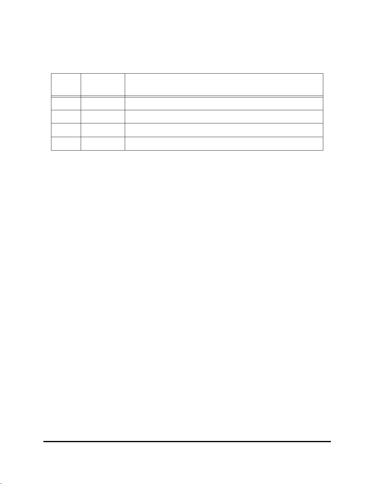
Document Revision History
Document Revision History
Rev.
No.
1.0 10/2002 Chapter 21, Electrical Specifications
2.0 05/2003 Chapter 21, Electrical Specifications
3.0 08/2003 Chapter 4, QSPISEL bit
4.0 10/29/03 Chapter 21, Electrical Specifications
nc...
I
cale Semiconductor,
Date Substantive Change(s)
Frees
2 MCF5249UM MOTOROLA
For More Information On This Product,
Go to: www.freescale.com

nc...
I
cale Semiconductor,
Frees
Freescale Semiconductor, Inc.
TABLE OF CONTENTS
Paragraph Page
Number Number
SECTION 1
INTRODUCTION 1
1.1 MCF5249 Overview .............................................................................................................1-1
1.2 MCF5249 Feature Introduction ............................................................................................1-1
1.3 MCF5249 Block Diagram .....................................................................................................1-2
1.4 MCF5249 Feature Details ....................................................................................................1-3
1.5 160 MAPBGA Ball Assignments ..........................................................................................1-5
1.6 MCF5249 Functional Overview ...........................................................................................1-6
1.6.1 ColdFire V2 Core ............................................................................................................1-6
1.6.2 DMA Controller ...............................................................................................................1-6
1.6.3 Enhanced Multiply and Accumulate Module (EMAC) .....................................................1-6
1.6.4 Instruction Cache ............................................................................................................1-6
1.6.5 Internal 96-KByte SRAM ................................................................................................1-6
1.6.6 DRAM Controller ............................................................................................................1-7
1.6.7 System Interface .............................................................................................................1-7
1.6.8 External Bus Interface ....................................................................................................1-7
1.6.9 Serial Audio Interfaces ...................................................................................................1-7
1.6.10 IEC958 Digital Audio Interfaces ......................................................................................1-7
1.6.11 Audio Bus .......................................................................................................................1-7
1.6.12 CD-ROM Encoder/Decoder ............................................................................................1-8
1.6.13 Dual UART Module .........................................................................................................1-8
1.6.14 Queued Serial Peripheral Interface QSPI .......................................................................1-8
1.6.15 Timer Module ..................................................................................................................1-8
1.6.16 IDE and SmartMedia Interfaces .....................................................................................1-9
1.6.17 Analog/Digital Converter (ADC) ......................................................................................1-9
1.6.18 Flash Memory Card Interface .........................................................................................1-9
1.6.19 I
1.6.20 Chip-Selects ...................................................................................................................1-9
1.6.21 GPIO Interface ................................................................................................................1-9
1.6.22 Interrupt Controller ..........................................................................................................1-9
1.6.23 JTAG ............................................................................................................................1-10
1.6.24 System Debug Interface ...............................................................................................1-10
1.6.25 Crystal and On-chip PLL ..............................................................................................1-10
2.1 Introduction ..........................................................................................................................2-1
2.2 GPIO ....................................................................................................................................2-4
2.3 MCF5249 BUS SIGNALS ....................................................................................................2-4
2.3.1 ADDRESS BUS ..............................................................................................................2-4
2.3.2 READ-WRITE CONTROL ..............................................................................................2-4
2.3.3 OUTPUT ENABLE ..........................................................................................................2-5
2.3.4 Data Bus .........................................................................................................................2-5
2.3.5 Transfer Acknowledge ....................................................................................................2-5
2.4 SDRAM Controller Signals ..................................................................................................2-5
2.5 CHIP SELECTS ...................................................................................................................2-5
2.6 ISA bus ................................................................................................................................2-6
2.7 bus buffer signals .................................................................................................................2-6
2
C Module ......................................................................................................................1-9
SECTION 2
SIGNAL DESCRIPTION
MOTOROLA Table of Contents TOC-1
For More Information On This Product,
Go to: www.freescale.com

nc...
I
cale Semiconductor,
Frees
Table of Contents
Paragraph Page
Number Number
2.8 I2C Module Signals ..............................................................................................................2-6
2.9 Serial Module Signals ..........................................................................................................2-6
2.10 Timer Module Signals ..........................................................................................................2-7
2.11 Serial Audio Interface Signals ..............................................................................................2-7
2.12 Digital Audio Interface Signals .............................................................................................2-9
2.13 Subcode interface ................................................................................................................2-9
2.14 Analog to Digital Converter (ADC) .......................................................................................2-9
2.15 Secure Digital/ MemoryStick card Interface .......................................................................2-10
2.16 Queued Serial Peripheral Interface (QSPI) .......................................................................2-10
2.17 Crystal Trim .......................................................................................................................2-11
2.18 Clock Out ...........................................................................................................................2-11
2.19 Debug and Test Signals ....................................................................................................2-11
2.19.1 Test Mode .....................................................................................................................2-11
2.19.2 High Impedance ...........................................................................................................2-11
2.19.3 Processor Clock Output ................................................................................................2-11
2.19.4 Debug Data ..................................................................................................................2-11
2.19.5 Processor Status ..........................................................................................................2-11
2.20 BDM/JTAG Signals ............................................................................................................2-12
2.20.1 Test Clock .....................................................................................................................2-12
2.20.2 Test Reset/Development Serial Clock ..........................................................................2-12
2.20.3 Test Mode Select/Break Point ......................................................................................2-13
2.20.4 Test Data Input/Development Serial Input ....................................................................2-13
2.20.5 Test Data Output/Development Serial Output ..............................................................2-13
2.21 Clock and Reset signals ....................................................................................................2-14
2.21.1 Reset In ........................................................................................................................2-14
2.21.2 System Bus input ..........................................................................................................2-14
Freescale Semiconductor, Inc.
SECTION 3
COLDFIRE CORE
3.1 Processor Pipelines .............................................................................................................3-1
3.2 Processor Register Description ...........................................................................................3-2
3.2.1 User Programming Model ...............................................................................................3-2
3.2.1.1 Data Registers (D0–D7) ............................................................................................3-2
3.2.1.2 Address Registers (A0–A6) .......................................................................................3-2
3.2.1.3 Stack Pointer (A7,SP) ................................................................................................3-2
3.2.1.4 Program Counter (PC) ...............................................................................................3-3
3.2.1.5 Condition Code Register (CCR) ................................................................................3-3
3.2.2 Enhanced Multiply Accumulate Module (EMAC) User Programming Model ..................3-4
3.2.2.1 EMAC Instruction Set Summary ................................................................................3-4
3.2.3 Supervisor Programming Model .....................................................................................3-5
3.2.3.1 Status Register (SR) ..................................................................................................3-6
3.2.3.2 Vector Base Register (VBR) ......................................................................................3-6
3.3 Exception Processing Overview ..........................................................................................3-7
3.4 Exception Stack Frame Definition ........................................................................................3-8
3.5 Processor Exceptions ........................................................................................................3-10
3.5.1 Access Error Exception ................................................................................................3-10
3.5.2 Address Error Exception ...............................................................................................3-10
3.5.3 Illegal Instruction Exception ..........................................................................................3-10
3.5.4 Divide By Zero ..............................................................................................................3-10
3.5.5 Privilege Violation .........................................................................................................3-11
3.5.6 Trace Exception ............................................................................................................3-11
TOC-2 MCF5249UM MOTOROLA
For More Information On This Product,
Go to: www.freescale.com

nc...
I
cale Semiconductor,
Frees
Freescale Semiconductor, Inc.
Paragraph Page
Number Number
3.5.7 Debug Interrupt .............................................................................................................3-11
3.5.8 RTE and Format Error Exceptions ................................................................................3-11
3.5.9 TRAP Instruction Exceptions ........................................................................................3-12
3.5.10 Interrupt Exception .......................................................................................................3-12
3.5.11 Fault-on-Fault Halt ........................................................................................................3-12
3.5.12 Reset Exception ...........................................................................................................3-12
3.6 Instruction Execution Timing ..............................................................................................3-12
3.6.1 Timing Assumptions .....................................................................................................3-13
3.6.2 MOVE Instruction Execution Times ..............................................................................3-13
3.7 Standard One Operand Instruction Execution Times ........................................................3-15
3.8 Standard Two Operand Instruction Execution Times ........................................................3-16
3.9 Miscellaneous Instruction Execution Times .......................................................................3-18
3.10 Branch Instruction Execution Times ..................................................................................3-19
Table of Contents
SECTION 4
PHASE-LOCKED LOOP AND CLOCK DIVIDERS
4.1 PLL Features .......................................................................................................................4-1
4.2 PLL Programming ................................................................................................................4-2
4.2.1 PLL Operation ................................................................................................................4-4
4.2.2 PLL Lock-in Time ............................................................................................................4-4
4..2.3 PLL Electrical Limits .......................................................................................................4-4
4.3 Audio Clock Generation .......................................................................................................4-5
4.4 Reduced Power Mode .........................................................................................................4-6
4.5 Recommended Settings ......................................................................................................4-6
SECTION 5
INSTRUCTION CACHE
5.1 Instruction Cache Features ..................................................................................................5-1
5.2 Instruction Cache Physical Organization .............................................................................5-1
5.3 Instruction Cache Operation ................................................................................................5-2
5.3.1 Interaction with Other Modules .......................................................................................5-2
5.3.2 Memory Reference Attributes .........................................................................................5-3
5.3.3 Cache Coherency and Invalidation .................................................................................5-3
5.3.4 Reset ..............................................................................................................................5-3
5.3.5 Cache Miss Fetch Algorithm/Line Fills ............................................................................5-3
5.4 Instruction Cache Programming Model ...............................................................................5-5
5.4.1 Instruction Cache Registers Memory Map ......................................................................5-5
5.4.2 Instruction Cache Register .............................................................................................5-6
5.4.2.1 Cache Control Register .............................................................................................5-6
5.4.2.2 Access Control Registers ..........................................................................................5-8
MOTOROLA Table of Contents TOC-3
For More Information On This Product,
Go to: www.freescale.com

nc...
I
cale Semiconductor,
Frees
Table of Contents
Paragraph Page
Number Number
Freescale Semiconductor, Inc.
SECTION 6
STATIC RAM (SRAM)
6.1 SRAM Features ...................................................................................................................6-1
6.2 SRAM Operation ..................................................................................................................6-1
6.3 SRAM Programming Model .................................................................................................6-1
6.3.1 SRAM Base Address Register .......................................................................................6-1
6.3.2 SRAM Initialization .........................................................................................................6-4
6.3.3 SRAM Initialization Code ................................................................................................6-4
6.3.4 Power Management .......................................................................................................6-4
SECTION 7
SYNCHRONOUS DRAM CONTROLLER MODULE
7.1 DRAM Features ...................................................................................................................7-1
7.1.1 Definitions .......................................................................................................................7-1
7.1.2 Block Diagram and Major Components ..........................................................................7-1
7.2 DRAM Controller Operation .................................................................................................7-2
7.2.1 DRAM Controller Registers ............................................................................................7-2
7.3 Synchronous Operation .......................................................................................................7-3
7.3.1 DRAM Controller Signals in Synchronous Mode ............................................................7-4
7.3.2 Synchronous Register Set ..............................................................................................7-5
7.3.2.1 DRAM Control Register (DCR) (Synchronous Mode) ...............................................7-5
7.3.2.2 DRAM Address and Control (DACR0/DACR1) (Synchronous Mode) .......................7-7
7.3.2.3 DRAM Controller Mask Registers (DMR0/DMR1) .....................................................7-9
7.3.3 General Synchronous Operation Guidelines ................................................................7-10
7.3.3.1 Address Multiplexing ...............................................................................................7-10
7.3.3.2 Interfacing Example .................................................................................................7-11
7.3.3.3 Burst Page Mode .....................................................................................................7-11
7.3.3.4 Continuous Page Mode ...........................................................................................7-13
7.3.3.5 Auto-Refresh Operation ...........................................................................................7-15
7.3.3.6 Self-Refresh Operation ............................................................................................7-16
7.3.4 Initialization Sequence ..................................................................................................7-17
7.3.4.1 Mode Register Settings ...........................................................................................7-17
7.4 SDRAM Example ...............................................................................................................7-18
7.4.1 SDRAM Interface Configuration ...................................................................................7-18
7.4.2 DCR Initialization ..........................................................................................................7-19
7.4.3 DACR Initialization ........................................................................................................7-19
7.4.4 DMR Initialization ..........................................................................................................7-21
7.4.5 Mode Register Initialization ..........................................................................................7-22
7.4.6 Initialization Code .........................................................................................................7-23
SECTION 8
BUS OPERATION
8.1 Bus Features .......................................................................................................................8-1
8.2 Bus And Control Signals ......................................................................................................8-1
8.2.1 Address Bus ...................................................................................................................8-1
8.2.2 Read/Write control ..........................................................................................................8-2
8.2.3 Transfer Acknowledge (TA) ............................................................................................8-2
8.2.4 Data Bus .........................................................................................................................8-2
8.2.5 Chip Selects ...................................................................................................................8-3
8.2.6 Output Enable .................................................................................................................8-3
TOC-4 MCF5249UM MOTOROLA
For More Information On This Product,
Go to: www.freescale.com

Freescale Semiconductor, Inc.
Paragraph Page
Number Number
8.3 Clock and Reset Signals ......................................................................................................8-3
8.3.1 Reset In ..........................................................................................................................8-4
8.3.2 System Bus Clock Output ...............................................................................................8-4
8.4 Bus Characteristics ..............................................................................................................8-4
8.5 Data Transfer Operation ......................................................................................................8-5
8.5.1 Bus Cycle Execution .......................................................................................................8-6
8.5.2 Read Cycle .....................................................................................................................8-7
8.5.3 Write Cycle .....................................................................................................................8-8
8.5.4 Back-to-Back Bus Cycles .............................................................................................8-10
8.5.5 Burst Cycles .................................................................................................................8-11
8.5.5.1 Line Transfers ..........................................................................................................8-11
8.5.5.2 Line Read Bus Cycles .............................................................................................8-11
8.5.5.3 Line Write Bus Cycles .............................................................................................8-12
8.6 Misaligned Operands .........................................................................................................8-14
8.7 Reset Operation .................................................................................................................8-15
8.7.1 Software Watchdog Reset ............................................................................................8-16
nc...
I
Table of Contents
SECTION 9
SYSTEM INTEGRATION MODULE
cale Semiconductor,
Frees
9.1 SIM Introduction ...................................................................................................................9-1
9.1.1 SIM Features ..................................................................................................................9-1
9.2 Programming Model ............................................................................................................9-1
9.2.1 SIM Register Memory Map .............................................................................................9-1
9.3 SIM Programming and Configuration ..................................................................................9-3
9.3.1 Module Base Address Registers ....................................................................................9-3
9.3.2 Device ID ........................................................................................................................9-5
9.3.3 Interrupt Controller ..........................................................................................................9-6
9.4 Interrupt Interface ................................................................................................................9-6
9.4.1 Primary controller Interrupt Registers .............................................................................9-6
9.4.1.1 Interrupt Mask Register .............................................................................................9-9
9.4.1.2 Interrupt Pending Register .......................................................................................9-10
9.4.2 Secondary Interrupt Controller Registers .....................................................................9-11
9.4.2.1 Interrupt Level Selection ..........................................................................................9-11
9.4.2.2 Interrupt Vector Generation .....................................................................................9-12
9.4.2.3 Spurious Vector Register .........................................................................................9-12
9.4.2.4 Secondary Interrupt Sources ...................................................................................9-12
9.4.3 Software interrupts .......................................................................................................9-15
9.5 System Protection And Reset Status .................................................................................9-15
9.5.1 Reset Status Register ...................................................................................................9-15
9.5.2 Software Watchdog Timer ............................................................................................9-16
9.5.2.1 System Protection Control Register ........................................................................9-18
9.5.2.2 Software Watchdog Interrupt Vector Register .........................................................9-19
9.5.2.3 Software Watchdog Service Register ......................................................................9-20
9.6 CPU STOP Instruction .......................................................................................................9-20
9.7 MCF5249 Bus Arbitration Control ......................................................................................9-20
9.7.1 Default Bus Master Park Register ................................................................................9-20
9.7.1.1 Internal Arbitration Operation ..................................................................................9-20
9.7.1.2 PARK Register Bit Configuration .............................................................................9-21
9.8 General Purpose I/Os ........................................................................................................9-23
9.8.1 General Purpose Inputs ................................................................................................9-23
9.8.1.1 General Purpose Input Interrupts ............................................................................9-25
9.8.2 General Purpose Outputs .............................................................................................9-26
MOTOROLA Table of Contents TOC-5
For More Information On This Product,
Go to: www.freescale.com

nc...
I
cale Semiconductor,
Frees
Table of Contents
Paragraph Page
Number Number
Freescale Semiconductor, Inc.
SECTION 10
CHIP-SELECT MODULE
10.1 Introduction ........................................................................................................................10-1
10.1.1 Chip Select Features ....................................................................................................10-1
10.2 Chip-Select Signals ...........................................................................................................10-1
10.2.1 Chip Selects .................................................................................................................10-1
10.2.1.1 CS0 .........................................................................................................................10-1
10.2.1.2 CS1/GPIO1 .............................................................................................................10-1
10.2.1.3 CS2/IDE-DIOR/GPIO13 and IDE-DIOW/GPIO14 ...................................................10-1
10.2.1.4 CS3/SRE/GPIO11 and SWE/GPIO12 .....................................................................10-2
10.2.2 Output Enable OE/gpio9 ...............................................................................................10-2
10.2.3 buffer enable signals - bufenb1 and bufenb2 ...............................................................10-2
10.2.4 IORDY - bus termination signal ....................................................................................10-2
10.3 MCF5249Chip-Select Operation ........................................................................................10-2
10.3.1 Chip-Select Module ......................................................................................................10-2
10.3.1.1 General Chip Select Operation ................................................................................10-3
10.3.1.1.1 Port Sizing ..........................................................................................................10-4
10.3.2 Global Chip-Select Operation .......................................................................................10-4
10.4 Programming Model ..........................................................................................................10-4
10.4.1 Chip-Select Registers Memory Map .............................................................................10-4
10.4.2 Chip Select Module Registers ......................................................................................10-6
10.4.2.1 Chip Select Address Register ..................................................................................10-6
10.4.2.2 Chip Select Mask Register ......................................................................................10-6
10.4.2.3 Chip Select Control Register ...................................................................................10-8
10.4.2.4 Code example .......................................................................................................10-10
SECTION 11
TIMER MODULE
11.1 Timer Module Overview .....................................................................................................11-1
11.2 Timer Features ..................................................................................................................11-1
11.3 Timer Signals .....................................................................................................................11-1
11.3.1 Timer Inputs ..................................................................................................................11-1
11.3.2 Timer Outputs ...............................................................................................................11-1
11.4 General-Purpose Timer Units ............................................................................................11-2
11.4.1 Selecting the Prescaler .................................................................................................11-3
11.4.2 Capture Mode ...............................................................................................................11-3
11.4.3 Configuring the Timer for Reference Compare .............................................................11-3
11.4.4 Configuring the Timer for Output Mode ........................................................................11-3
11.5 General-Purpose Timer Registers .....................................................................................11-3
11.5.1 Timer Mode Registers (TMR0, TMR1) .........................................................................11-4
11.5.2 Timer Reference Registers (TRR0, TRR1) ...................................................................11-5
11.5.3 Timer Capture Registers (TCR0, TCR1) ......................................................................11-5
11.5.4 Timer Counters (TCN0, TCN1) .....................................................................................11-6
11.5.5 Timer Event Registers (TER0, TER1) ..........................................................................11-6
11.5.6 Timer Initialization Example Code ................................................................................11-7
11.5.6.1 Timer 0 (Timer Mode Register) ...............................................................................11-7
11.5.6.2 Timer 0 (Timer Reference Register 0) .....................................................................11-8
11.5.6.3 Timer 1 (Timer Mode Register 1) ............................................................................11-8
TOC-6 MCF5249UM MOTOROLA
For More Information On This Product,
Go to: www.freescale.com

Freescale Semiconductor, Inc.
Paragraph Page
Number Number
Table of Contents
SECTION 12
ANALOG TO DIGITAL CONVERTER (ADC)
12.1 ADC Overview ...................................................................................................................12-1
12.2 ADC Functionality ..............................................................................................................12-2
SECTION 13
IDE AND FLASHMEDIA INTERFACE
13.1 IDE and SmartMedia Overview .........................................................................................13-1
13.1.1 Buffer enables bufenb1, bufenB2, and associated logic. .............................................13-2
13.1.2 Generation of IDE-DIOR, IDE-DIOW, SRE, SWE ........................................................13-4
13.1.3 Cycle termination on CS2, CS3 (DIOR, DIOW, SRE, SWE) ........................................13-5
13.2 SmartMedia Interface Setup ..............................................................................................13-6
13.2.1 SmartMedia timing ........................................................................................................13-7
13.3 Setting Up The IDE Interface .............................................................................................13-8
nc...
I
cale Semiconductor,
13.3.1 IDE timing diagram .......................................................................................................13-8
13.4 FlashMedia Interface .......................................................................................................13-10
13.4.1 FlashMedia Interface Registers ..................................................................................13-10
13.4.1.1 FlashMedia Clock Generation and Configuration ..................................................13-11
13.4.2 FlashMedia Interface Operation .................................................................................13-12
13.4.2.1 FlashMedia Command Registers in MemoryStick Mode .......................................13-13
13.4.2.2 FlashMedia Command Register 1 in Secure Digital Mode ....................................13-13
13.4.2.3 FLASHMEDIA COMMAND REGISTER 2 in Secure Digital Mode ........................13-14
13.4.3 FlashMedia Data Register ..........................................................................................13-15
13.4.3.1 FlashMedia Status Register ..................................................................................13-15
13.4.4 FlashMedia Interrupt Interface ....................................................................................13-15
13.4.5 FlashMedia Interface Operation in MemoryStick Mode ..............................................13-16
13.4.5.1 Reading Data From the MemoryStick ...................................................................13-17
13.4.5.2 Writing Data to the MemoryStick ...........................................................................13-18
13.4.5.3 Interrupt From MemoryStick ..................................................................................13-19
13.4.6 FlashMedia interface Operation in Secure Digital (SD) mode ....................................13-20
13.4.6.1 Sent Command To Card ........................................................................................13-20
13.4.6.2 Write Data To Card ................................................................................................13-21
13.4.7 Commonly used commands in SD mode ...................................................................13-23
13.4.7.1 Send Command To Card (No Data) ......................................................................13-23
13.4.7.2 Send Command To Card (Receive Multiple Data Blocks and Status) ..................13-24
13.4.7.3 Send Command To Card (Write Multiple Data Blocks) .........................................13-25
Frees
SECTION 14
DMA CONTROLLER MODULE
14.1 DMA Features ....................................................................................................................14-2
14.2 DMA Signal Description .....................................................................................................14-2
14.2.1 DMA Request ...............................................................................................................14-2
14.3 DMA Module Overview ......................................................................................................14-2
14.4 DMA Programming Model .................................................................................................14-3
14.4.1 REQUEST source selection .........................................................................................14-5
14.4.2 Source Address Register ..............................................................................................14-8
14.4.3 FLASHmEDIA DATA RegisterS ...................................................................................14-9
14.4.4 Byte Count Register .....................................................................................................14-9
14.4.5 DMA Control Register .................................................................................................14-10
MOTOROLA Table of Contents TOC-7
For More Information On This Product,
Go to: www.freescale.com

Table of Contents
Paragraph Page
Number Number
14.4.6 DMA Status Register ..................................................................................................14-13
14.4.7 DMA Interrupt Vector Register ...................................................................................14-15
14.5 Transfer Request Generation ..........................................................................................14-15
14.5.1 Cycle-Steal Mode .......................................................................................................14-15
14.5.2 Continuous Mode .......................................................................................................14-15
14.6 Data Transfer Modes .......................................................................................................14-16
14.6.1 Dual-Address Transaction ..........................................................................................14-16
14.6.1.1 Dual-Address Read ...............................................................................................14-16
14.6.1.2 Dual-Address Write ...............................................................................................14-16
14.7 DMA Transfer Functional Description .............................................................................14-16
14.7.1 Channel Initialization and Startup ...............................................................................14-17
14.7.1.1 Channel Prioritization ............................................................................................14-17
14.7.1.2 Programming the DMA ..........................................................................................14-17
14.7.2 Data Transfer ..............................................................................................................14-18
14.7.2.1 Periphery Request Operation ................................................................................14-18
14.7.2.2 Auto Alignment ......................................................................................................14-18
nc...
I
14.7.2.3 Bandwidth Control .................................................................................................14-19
14.7.3 Channel Termination ..................................................................................................14-19
14.7.3.1 Error Conditions .....................................................................................................14-19
14.7.3.2 Interrupts ...............................................................................................................14-19
Freescale Semiconductor, Inc.
cale Semiconductor,
Frees
SECTION 15
UART MODULES
15.1 Module Overview ...............................................................................................................15-1
15.1.1 Serial Communication Channel ....................................................................................15-2
15.1.2 Baud-Rate Generator/Timer .........................................................................................15-2
15.1.3 Interrupt Control Logic ..................................................................................................15-2
15.2 UART Module Signal Definitions .......................................................................................15-3
15.2.1 Transmitter Serial Data Output .....................................................................................15-3
15.2.2 Receiver Serial Data Input ............................................................................................15-3
15.2.3 Request-To-Send .........................................................................................................15-4
15.2.4 Clear-To-Send ..............................................................................................................15-4
15.3 Operation ...........................................................................................................................15-4
15.3.1 Baud-Rate Generator/Timer .........................................................................................15-4
15.3.2 Transmitter and Receiver Operating Modes .................................................................15-5
15.3.2.1 Transmitter ..............................................................................................................15-5
15.3.2.2 Receiver ..................................................................................................................15-7
15.3.2.3 Receiver FIFO .........................................................................................................15-8
15.3.3 Looping Modes .............................................................................................................15-9
15.3.3.1 Automatic Echo Mode .............................................................................................15-9
15.3.3.2 Local Loopback Mode .............................................................................................15-9
15.3.3.3 Remote Loopback Mode .......................................................................................15-10
15.3.4 Multidrop Mode ...........................................................................................................15-10
15.3.5 Bus Operation .............................................................................................................15-12
15.3.5.1 Read Cycles ..........................................................................................................15-12
15.3.5.2 Write Cycles ..........................................................................................................15-12
15.3.5.3 Interrupt Acknowledge Cycles ...............................................................................15-12
15.4 Register Description and Programming ...........................................................................15-12
15.4.1 Register Description ...................................................................................................15-12
15.4.1.1 Mode Register 1 (UMR1n) .....................................................................................15-13
15.4.1.2 Mode Register 2 (UMR2n) .....................................................................................15-15
TOC-8 MCF5249UM MOTOROLA
For More Information On This Product,
Go to: www.freescale.com

nc...
I
cale Semiconductor,
Frees
Freescale Semiconductor, Inc.
Paragraph Page
Number Number
15.4.1.3 Status Registers (USRn) .......................................................................................15-18
15.4.1.4 Clock-Select Registers (USCRn) ...........................................................................15-19
15.4.1.5 Command Registers (UCRn) .................................................................................15-20
15.4.1.6 Miscellaneous Commands ....................................................................................15-20
15.4.1.6.1 Reset Mode Register Pointer ...........................................................................15-21
15.4.1.6.2 Reset Receiver .................................................................................................15-21
15.4.1.6.3 Reset Transmitter .............................................................................................15-21
15.4.1.6.4 Reset Error Status ............................................................................................15-21
15.4.1.6.5 Reset Break-Change Interrupt .........................................................................15-21
15.4.1.6.6 Start Break .......................................................................................................15-21
15.4.1.6.7 Stop Break ........................................................................................................15-21
15.4.1.7 Transmitter Commands .........................................................................................15-21
15.4.1.7.1 No Action Taken ...............................................................................................15-22
15.4.1.7.2 Transmitter Enable ...........................................................................................15-22
15.4.1.7.3 Transmitter Disable ..........................................................................................15-22
15.4.1.7.4 Do Not Use .......................................................................................................15-22
15.4.1.8 Receiver Commands .............................................................................................15-22
15.4.1.8.1 No Action Taken ...............................................................................................15-22
15.4.1.8.2 Receiver Enable ...............................................................................................15-22
15.4.1.8.3 Receiver Disable ..............................................................................................15-23
15.4.1.8.4 Do Not Use .......................................................................................................15-23
15.4.1.9 Receiver Buffer Registers (UBRn) .........................................................................15-23
15.4.1.10 Transmitter Buffer Registers (UTBn) .....................................................................15-23
15.4.1.11 Input Port Change Registers UIPCRn) ..................................................................15-24
15.4.1.12 Auxiliary Control Registers (UACRn) .....................................................................15-24
15.4.1.13 Interrupt Status Registers (UISRn) ........................................................................15-25
15.4.1.14 Interrupt Mask Registers UIMRn) ..........................................................................15-26
15.4.1.15 Timer Upper Preload Register (UBG1n) ................................................................15-27
15.4.1.16 Timer Upper Preload Register 2 (UBG2n) .............................................................15-27
15.4.1.17 Interrupt Vector Registers (UIVRn) ........................................................................15-27
15.4.1.18 Input Port Registers (UIPn) ...................................................................................15-28
15.4.1.19 Output Port Data Registers (UOP1n) ....................................................................15-28
15.4.2 Programming ..............................................................................................................15-29
15.4.2.1 UART Module Initialization ....................................................................................15-29
15.4.2.2 I/O Driver Example ................................................................................................15-29
15.4.1.3 Interrupt Handling ..................................................................................................15-29
15.5 UART Module Initialization Sequence .............................................................................15-30
Table of Contents
SECTION 16
QUEUED SERIAL PERIPHERAL INTERFACE (QSPI) MODULE
16.1 Overview ............................................................................................................................16-1
16.2 Features .............................................................................................................................16-1
16.3 Module Description ............................................................................................................16-1
16.3.1 Interface and Pins .........................................................................................................16-1
16.3.2 Internal Bus Interface ...................................................................................................16-2
16.4 Operation ...........................................................................................................................16-3
16.4.1 QSPI RAM ....................................................................................................................16-3
16.4.1.1 Transmit RAM ..........................................................................................................16-5
16.4.1.2 Receive RAM ...........................................................................................................16-5
16.4.1.3 Command RAM .......................................................................................................16-5
16.4.2 Baud Rate Selection .....................................................................................................16-6
MOTOROLA Table of Contents TOC-9
For More Information On This Product,
Go to: www.freescale.com

Table of Contents
Paragraph Page
Number Number
16.4.3 Transfer Delays ............................................................................................................16-6
16.4.4 Transfer Length ............................................................................................................16-7
16.4.5 Data Transfer ................................................................................................................16-7
16.5 Programming Model ..........................................................................................................16-8
16.5.1 QSPI Mode Register (QMR) .........................................................................................16-8
16.5.2 QSPI Delay Register (QDLYR) ...................................................................................16-10
16.5.3 QSPI Wrap Register (QWR) .......................................................................................16-10
16.5.4 QSPI Interrupt Register (QIR) ....................................................................................16-11
16.5.5 QSPI Address Register (QAR) ...................................................................................16-12
16.5.6 QSPI Data Register (QDR) .........................................................................................16-13
16.5.7 Command RAM Registers (QCR0–QCR15) ...............................................................16-13
16.5.8 Programming Example ...............................................................................................16-15
Freescale Semiconductor, Inc.
SECTION 17
AUDIO FUNCTIONS
nc...
I
cale Semiconductor,
Frees
17.1 Audio Interface Overview ...................................................................................................17-1
17.1.1 Audio Interface Structure ..............................................................................................17-2
17.1.1.1 Audio Interrupt Mask and Interrupt Status Registers ...............................................17-3
17.2 Serial Audio Interface (IIS/EIAJ) ........................................................................................17-5
17.2.1 IIS/EIAJ Transmitter Descriptions .................................................................................17-9
17.2.2 IIS/EIAJ Transmitter Interrupts .....................................................................................17-9
17.2.3 IIS/EIAJ Receiver Descriptions .....................................................................................17-9
17.3 Digital Audio Interface (EBU) ...........................................................................................17-10
17.3.1 IEC958 Receive Interface ...........................................................................................17-13
17.3.1.1 Audio Data Reception ............................................................................................17-13
17.3.1.2 Control Channel Reception ...................................................................................17-13
17.3.1.3 Control Channel Interrupt (IEC958 “C” Channel New Frame) ...............................17-13
17.3.1.4 Validity Flag Reception ..........................................................................................17-13
17.3.1.5 IEC958 Exception Definition ..................................................................................17-14
17.3.1.6 EBU Extracted Clock .............................................................................................17-14
17.3.1.7 Reception of User Channel and CD-subcode Over IEC958 Receiver ..................17-14
17.3.1.8 U and Q Receive Register Interrupts .....................................................................17-16
17.3.1.9 Behavior of User Channel Receive Interface (CD Data) .......................................17-16
17.3.1.10 Behavior of User Channel Receive Interface (non-CD data) .................................17-18
17.3.2 IEC958 Transmit Interface ..........................................................................................17-18
17.3.2.1 Transmit “C” Channel ............................................................................................17-18
17.3.2.2 IEC958 Transmitter Exception Conditions .............................................................17-19
17.3.2.3 IEC958-3 Ed2 and Tech 3250-E Standards Compliance ......................................17-19
17.3.2.4 Transmission of U-Channel and CD Subcode Data ..............................................17-20
17.3.3 CD Subcode Interrupts ...............................................................................................17-21
17.3.3.1 Free Running Counter Synchronization ................................................................17-22
17.3.3.2 Controlling the SFSY Sync Position ......................................................................17-22
17.3.4 Inserting CD User Channel Data Into IEC958 Transmit Data .....................................17-22
17.4 Processor Interface Overview ..........................................................................................17-23
17.4.1 Data Exchange Register Descriptions ........................................................................17-23
17.4.2 Data Exchange Register Overview .............................................................................17-24
17.4.2.1 Data In Selection ...................................................................................................17-25
17.4.3 PDIR and PDOR Field Formatting ..............................................................................17-27
17.4.4 Overrun and Underrun with PDIR and PDOR Registers ............................................17-27
17.4.5 Automatic Resynchronization of FIFOs ......................................................................17-28
17.4.6 Audio Interrupts ..........................................................................................................17-30
TOC-10 MCF5249UM MOTOROLA
For More Information On This Product,
Go to: www.freescale.com

nc...
I
cale Semiconductor,
Frees
Freescale Semiconductor, Inc.
Paragraph Page
Number Number
17.4.6.1 AudioTick Interrupts ...............................................................................................17-30
17.4.6.2 PDIR1, PDIR2, and PDIR3, Exceptions ................................................................17-30
17.4.6.3 PDOR1, PDOR2, and PDOR3 Exceptions ............................................................17-30
17.4.6.4 Audio Interrupt Routines and Timing .....................................................................17-32
17.4.7 CD-ROM Block Encoder and Decoder .......................................................................17-33
17.4.7.1 CD-ROM Decoder Interrupts .................................................................................17-35
17.4.7.2 CD-ROM Encoder Interrupts .................................................................................17-36
17.5 DMA Channel Interaction .................................................................................................17-36
17.6 Phase/Frequency Determination and Xtrim Function ......................................................17-37
17.6.1 Incoming Source Frequency Measurement ................................................................17-37
17.6.1.1 Filtering for the Discrete Time Oscillator ...............................................................17-40
17.6.2 XTRIM Option - Locking Xtal Clock to Incoming Signal ..............................................17-40
17.6.3 XTRIM Internal Logic ..................................................................................................17-40
17.7 Audio Interface Memory Map ...........................................................................................17-41
Table of Contents
SECTION 18
I2C MODULES
18.1 I2C Overview ......................................................................................................................18-1
18.2 I
18.3 I
18.4 I
18.4.1 START Signal ...............................................................................................................18-3
18.4.2 Slave Address Transmission ........................................................................................18-3
18.4.3 Data Transfer ................................................................................................................18-4
18.4.4 Repeated START Signal ..............................................................................................18-4
18.4.5 STOP Signal .................................................................................................................18-4
18.4.6 Arbitration Procedure ....................................................................................................18-4
18.4.7 Clock Synchronization ..................................................................................................18-4
18.4.8 Handshaking .................................................................................................................18-5
18.4.9 Clock Stretching ...........................................................................................................18-5
18.5 Programming Model ..........................................................................................................18-5
18.5.1 I
18.5.2 I
18.5.3 I
18.5.4 I
18.5.5 I
18.6 I
18.6.1 Initialization Sequence ................................................................................................18-12
18.6.2 Generation of START .................................................................................................18-12
18.6.3 Post-Transfer Software Response .............................................................................18-13
18.6.4 Slave Mode .................................................................................................................18-14
18.6.5 Arbitration Lost ...........................................................................................................18-15
2
C Interface Features .......................................................................................................18-1
2
C System Configuration ..................................................................................................18-2
2
C Protocol .......................................................................................................................18-3
2
C Address Registers (MADR) ....................................................................................18-6
2
C Frequency Divider Registers (MFDR) ....................................................................18-6
2
C Control Registers (MBCR) ......................................................................................18-8
2
C Status Registers (MBSR) .....................................................................................18-10
2
C Data I/O Registers (MBDR) ..................................................................................18-11
2
C Programming Examples ............................................................................................18-12
SECTION 19
DEBUG SUPPORT
19.1 Breakpoint (BKPT) .............................................................................................................19-1
19.1.1 Debug Support Signals ................................................................................................19-1
19.1.2 Debug Data (DDATA[3:0]) ............................................................................................19-1
19.1.3 Development Serial Clock (DSCLK) .............................................................................19-2
19.1.4 Development Serial Input (DSI) ....................................................................................19-2
MOTOROLA Table of Contents TOC-11
For More Information On This Product,
Go to: www.freescale.com

nc...
I
cale Semiconductor,
Frees
Table of Contents
Paragraph Page
Number Number
19.1.5 Development Serial Output (DSO) ...............................................................................19-2
19.1.6 Processor Status (PST[3:0]) .........................................................................................19-2
19.1.7 Processor Status Clock (PSTCLK) ...............................................................................19-3
19.2 Real-Time Trace Support ..................................................................................................19-4
19.2.1 Processor Status Signal Encoding ...............................................................................19-4
19.2.1.1 Continue Execution (PST = $0) ...............................................................................19-4
19.2.1.2 Begin Execution of an Instruction (PST = $1) .........................................................19-4
19.2.1.3 Entry into User Mode (PST = $3) ............................................................................19-4
19.2.1.4 Begin Execution of PULSE or WDDATA instructions (PST = $4) ...........................19-4
19.2.1.5 Begin Execution of Taken Branch (PST = $5) .........................................................19-5
19.2.1.6 Begin Execution of RTE Instruction (PST = $7) ......................................................19-6
19.2.1.7 Begin Data Transfer (PST = $8–$B) .......................................................................19-6
19.2.1.8 Exception Processing (PST = $C) ...........................................................................19-6
19.2.1.9 Emulator Mode Exception Processing (PST = $D) .................................................19-6
19.2.1.10 Processor Stopped (PST = $E) ...............................................................................19-6
19.2.1.11 Processor Halted (PST = $F) ..................................................................................19-6
19.3 Background-Debug Mode (BDM) ......................................................................................19-6
19.3.1 CPU Halt .......................................................................................................................19-7
19.3.2 BDM Serial Interface ....................................................................................................19-7
19.3.2.1 Receive Packet Format ...........................................................................................19-8
19.3.2.2 Transmit Packet Format ..........................................................................................19-9
19.3.3 BDM Command Set ......................................................................................................19-9
19.3.3.1 BDM Command Set Summary ................................................................................19-9
19.3.3.2 ColdFire BDM Commands .......................................................................................19-9
19.3.3.3 Command Sequence Diagram ..............................................................................19-11
19.3.3.4 Command Set Descriptions ...................................................................................19-13
19.3.3.4.1 Read Address/Data Register (RAREG/RDREG) .............................................19-13
19.3.3.4.2 Write Address/Data Register (WAREG and WDREG) .....................................19-13
19.3.3.4.3 Read Memory Location (READ) .......................................................................19-14
19.3.3.4.4 Write Memory Location (WRITE) .....................................................................19-16
19.3.3.4.5 Dump Memory Block (DUMP) ..........................................................................19-17
19.3.3.4.6 Fill Memory Block (FILL) ..................................................................................19-18
19.3.3.4.7 Resume Execution (GO) ..................................................................................19-20
19.3.3.4.8 No Operation (NOP) .........................................................................................19-20
19.3.3.4.9 Read Control Register (RCREG) .....................................................................19-21
19.3.3.4.10 Write Control Register (WCREG) .....................................................................19-22
19.3.3.4.11 Read Debug Module Register (RDMREG) .......................................................19-22
19.3.3.4.12 Write Debug Module Register (WDMREG) ......................................................19-23
19.3.3.4.13 Unassigned Opcodes .......................................................................................19-24
19.3.3.5 BDM Accesses of the EMAC Registers .................................................................19-24
19.4 Real-Time Debug Support ...............................................................................................19-25
19.4.1 Theory of Operation ....................................................................................................19-26
19.4.1.1 Emulator Mode ......................................................................................................19-27
19.4.1.2 Debug Module Hardware .......................................................................................19-27
19.4.1.2.1 Reuse of Debug Module Hardware (Rev. A) ....................................................19-27
19.4.2 Programming Model ...................................................................................................19-28
19.4.2.1 Address Breakpoint Registers ...............................................................................19-28
19.4.2.2 Address Attribute Trigger Register ........................................................................19-29
19.4.2.3 Program Counter Breakpoint Register (PBR, PBMR) ...........................................19-31
19.4.2.4 Data Breakpoint Registers (DBR, DBMR) .............................................................19-32
19.4.2.5 Trigger Definition Register (TDR) ..........................................................................19-34
19.4.2.6 Configuration/Status Register (CSR) .....................................................................19-36
Freescale Semiconductor, Inc.
TOC-12 MCF5249UM MOTOROLA
For More Information On This Product,
Go to: www.freescale.com

nc...
I
cale Semiconductor,
Frees
Freescale Semiconductor, Inc.
Paragraph Page
Number Number
19.4.2.7 BDM Address Attribute (BAAR) .............................................................................19-39
19.4.3 Concurrent BDM and Processor Operation ................................................................19-40
19.4.4 Motorola-Recommended BDM Pinout ........................................................................19-41
Table of Contents
SECTION 20
IEEE 1149.1 TEST ACCESS PORT (JTAG)
20.1 JTAG Overview ..................................................................................................................20-1
20.2 JTAG Signal Descriptions .................................................................................................20-2
20.2.1 Test Clock - (TCK) ........................................................................................................20-3
20.2.2 Test Reset/Development Serial Clock - (TRST/DSCLK) ..............................................20-3
20.2.3 Test Mode Select/ Breakpoint (TMS/BKPT) .................................................................20-3
20.2.4 Test Data Input/Development Serial Input - (TDI/DSI) .................................................20-4
20.2.5 Test Data Output/Development Serial Output - (TDO/DSO) ........................................20-4
20.3 TAP Controller ...................................................................................................................20-4
20.4 JTAG Registers .................................................................................................................20-6
20.4.1 JTAG Instruction Shift Register ...................................................................................20-6
20.4.1.1 EXTEST Instruction .................................................................................................20-6
20.4.1.2 IDCODE ...................................................................................................................20-6
20.4.1.3 SAMPLE/PRELOAD Instruction ..............................................................................20-7
20.4.1.4 CLAMP Instruction ...................................................................................................20-7
20.4.1.5 HIGHZ Instruction ....................................................................................................20-7
20.4.1.6 BYPASS Instruction .................................................................................................20-7
20.4.2 IDcode Register ............................................................................................................20-8
20.4.3 JTAG Boundary Scan Register ....................................................................................20-8
20.4.4 JTAG Bypass Register .................................................................................................20-9
20.5 Restrictions ........................................................................................................................20-9
20.6 Disabling IEEE 1149.1A Standard Operation ....................................................................20-9
20.7 MCF5249 BSDL File ........................................................................................................20-10
20.8 Obtaining the IEEE 1149.1A Standard ............................................................................20-22
SECTION 21
ELECTRICAL SPECIFICATIONS
21.1 Supply Voltage Sequencing and Separation Cautions ......................................................21-3
21.2 JTAG Timing Definition IIS Module AC Timing Specifications .........................................21-18
SECTION 22
MECHANICAL DATA
22.1 Package .............................................................................................................................22-1
22.2 Pin Assignment ..................................................................................................................22-1
APPENDIX A
REGISTER MEMORY MAP
MOTOROLA Table of Contents TOC-13
For More Information On This Product,
Go to: www.freescale.com

Table of Contents
Paragraph Page
Number Number
nc...
I
Freescale Semiconductor, Inc.
cale Semiconductor,
Frees
Intentionally
Left
Blank
TOC-14 MCF5249UM MOTOROLA
For More Information On This Product,
Go to: www.freescale.com

Freescale Semiconductor, Inc.
nc...
I
cale Semiconductor,
Frees
LIST OF FIGURES
Page
Number
Figure 1-1 MCF5249 Block Diagram .................................................................................. 1-2
Figure 3-1 V2 ColdFire Processor Core Pipelines ............................................................. 2-1
Figure 3-2 User Programming Model ................................................................................. 2-3
Figure 3-3 Supervisor Programming Model ....................................................................... 2-5
Figure 3-4 Vector Base Register (VBR) ............................................................................. 2-6
Figure 3-5 Exception Stack Frame Form ........................................................................... 2-9
Figure 4-1 Phase-Locked Loop Module Block Diagram ..................................................... 4-1
Figure 5-1 Instruction Cache Block Diagram ...................................................................... 5-2
Figure 7-1 Synchronous DRAM Controller Block Diagram ................................................ 7-2
Figure 7-2 MCF5249 SDRAM Interface ............................................................................. 7-5
Figure 7-3 DRAM Control Register (DCR) (Synchronous Mode) ....................................... 7-5
Figure 7-4 DACR0 and DACR1 (Synchronous Mode) ....................................................... 7-7
Figure 7-5 DRAM Controller Mask Registers (DMR0 and DMR1) ..................................... 7-9
Figure 7-6 Burst Read SDRAM Access ........................................................................... 7-12
Figure 7-7 Burst Write SDRAM Access ............................................................................ 7-13
Figure 7-8 Synchronous, Continuous Page-Mode Access—Consecutive Reads ............ 7-14
Figure 7-9 Synchronous, Continuous Page-Mode Access—Read after Write ................. 7-15
Figure 7-10 Auto-Refresh Operation .................................................................................. 7-16
Figure 7-11 Self-Refresh Operation ................................................................................... 7-16
Figure 7-12 Mode Register Set (mrs) Command ............................................................... 7-18
Figure 7-13 Initialization Values for DCR ........................................................................... 7-19
Figure 7-14 SDRAM Configuration ..................................................................................... 7-20
Figure 7-15 DACR Register Configuration ......................................................................... 7-20
Figure 7-16 DMR0 Register ............................................................................................... 7-21
Figure 7-17 Mode Register Mapping to MCF5249 A[31:0] ................................................. 7-22
Figure 8-1 Connections for External Memory Port Sizes ................................................... 8-3
Figure 8-2 Signal Relationship to BCLK for Non-DRAM Access ........................................ 8-5
Figure 8-3 Read Cycle Flowchart ....................................................................................... 8-7
Figure 8-4 Basic Read Bus Cycle ...................................................................................... 8-7
Figure 8-5 Write Cycle Flowchart ....................................................................................... 8-9
Figure 8-6 Basic Write Bus Cycle ....................................................................................... 8-9
Figure 8-7 Back-to-Back Bus Cycles ................................................................................ 8-10
Figure 8-8 Line Read Burst (one wait cycle) .................................................................... 8-12
Figure 8-9 Line Read Burst (no wait cycles) .................................................................... 8-12
Figure 8-10 Line Write Burst (no wait cycles) ..................................................................... 8-13
Figure 8-11 Line Read Burst-Inhibited ............................................................................... 8-13
Figure 8-12 Line Write Burst with One Wait State .............................................................. 8-14
Figure 8-13 Line Write Burst-Inhibited ................................................................................ 8-14
Figure 8-14 Misaligned Longword Transfer ........................................................................ 8-15
Figure 8-15 Misaligned Word Transfer ............................................................................... 8-15
Figure 8-16 Master Reset Timing ....................................................................................... 8-16
Figure 8-17 Software Watchdog Reset Timing .................................................................. 8-17
Figure 9-1 MCF5249 Unterminated Access Recovery ..................................................... 9-17
Figure 9-2 General-Purpose Pin Logic for Pin ddata3/gpio34 .......................................... 9-27
Figure 11-1 Timer Block Diagram Module Operation ......................................................... 11-2
Figure 12-1 ADC with On-chip and External Parts ............................................................. 12-2
Figure 13-1 Bus Setup with IDE and SmartMedia Interface ............................................... 13-1
Figure 13-2 Buffer Enables (BUFENB1 and BUFENB2) .................................................... 13-2
Figure 13-3 DIOR and SRE Timing Diagram ..................................................................... 13-5
Figure 13-4 Non-IORDY Controlled IDE/SmartMedia TA Timing ....................................... 13-6
Figure 13-5 CS2 (DIOR, DIOW) and CS3 (SRE, SWE) Cycle Timing ............................... 13-6
MOTOROLA List of Figures LOF-1
For More Information On This Product,
Go to: www.freescale.com

nc...
I
cale Semiconductor,
Frees
Freescale Semiconductor, Inc.
List of Figures
Figure 13-6 SmartMedia Timing ..........................................................................................13-7
Figure 13-7 IDE Timing .......................................................................................................13-8
Figure 13-8 FlashMedia Block Diagram ............................................................................13-10
Figure 13-9 One Interface Shift Register ..........................................................................13-12
Figure 13-10 Reading Data From MemoryStick ..................................................................13-17
Figure 13-11 Reading Data From MemoryStick Timing ......................................................13-17
Figure 13-12 Writing Data To MemoryStick ........................................................................13-18
Figure 13-13 Writing Data to MemoryStick Timing .............................................................13-18
Figure 13-14 Interrupt From MemoryStick ..........................................................................13-19
Figure 13-15 Interrupt From MemoryStick ..........................................................................13-19
Figure 13-16 Sent Command To Card ................................................................................13-20
Figure 13-17 Write Data To Card With Busy .......................................................................13-21
Figure 13-18 Write Data To Card Without Busy ..................................................................13-22
Figure 13-19 Read Data From Card ...................................................................................13-23
Figure 14-1 DMA Signal Diagram .......................................................................................14-1
Figure 14-2 Dual Address Transfer .....................................................................................14-3
Figure 15-1 UART Block Diagram .......................................................................................15-1
Figure 15-2 External and Internal Interface Signals ............................................................15-3
Figure 15-3 Baud-Rate Timer Generator Diagram ..............................................................15-4
Figure 15-4 Transmitter and Receiver Functional Diagram ................................................15-5
Figure 15-5 Transmitter Timing Diagram ............................................................................15-6
Figure 15-6 Receiver Timing Diagram ................................................................................15-7
Figure 15-7 Looping Modes Functional Diagram ..............................................................15-10
Figure 15-8 Multidrop Mode Timing Diagram ....................................................................15-11
Figure 15-9 UART Software Flowchart (1 of 5) .................................................................15-31
Figure 15-10 UART Software Flowchart (2 of 5) .................................................................15-32
Figure 15-11 UART Software Flowchart (3 of 5) .................................................................15-33
Figure 15-12 UART Software Flowchart (4 of 5) .................................................................15-34
Figure 15-13 UART Software Flowchart (5 of 5) .................................................................15-35
Figure 16-1 QSPI Block Diagram ........................................................................................16-2
Figure 16-2 QSPI RAM Model ............................................................................................16-4
Figure 16-3 QSPI Mode Register (QSPIMR) ......................................................................16-8
Figure 16-4 QSPI Clocking and Data Transfer Example ....................................................16-9
Figure 16-5 QSPI Delay Register (QDLYR) ......................................................................16-10
Figure 16-6 QSPI Wrap Register (QWR) ..........................................................................16-10
Figure 16-7 QSPI Interrupt Register (QIR) ........................................................................16-11
Figure 16-8 QSPI Address Register (QAR) ......................................................................16-13
Figure 16-9 QSPI Data Register (QDR) ............................................................................16-13
Figure 16-10 Command RAM Registers (QCR0–QCR15) ..................................................16-14
Figure 16-11 QSPI Timing ..................................................................................................16-15
Figure 17-1 Audio Interface Block Diagram ........................................................................17-2
Figure 17-2 IIS/EIAJ Timing Diagram (16 SCLK edges per word) ......................................17-9
Figure 17-3 IIS/EIAJ timing diagram (24 or 32 SCLK edges per word) ............................17-10
Figure 17-4 CD-Subcode Interface ...................................................................................17-20
Figure 17-5 Data Format on CD-Subcode Interface Out ..................................................17-21
Figure 17-6 Processor/Audio Module Interface .................................................................17-23
Figure 17-7 Automatic Resynchronization FSM of left-right FIFOs ...................................17-28
Figure 17-8 Audio Transmit / Receive FIFOs ....................................................................17-33
Figure 17-9 Block Decoder ...............................................................................................17-35
Figure 17-10 Block Encoder ................................................................................................17-36
Figure 17-11 Frequency Measurement Circuit ....................................................................17-38
Page
Number
LOF-2 MCF5249UM MOTOROLA
For More Information On This Product,
Go to: www.freescale.com

nc...
I
cale Semiconductor,
Frees
Freescale Semiconductor, Inc.
Figure 17-12 XTRIM External Circuit .................................................................................. 17-40
Figure 17-13 PDM Modulator Used on Xtrim Output .......................................................... 17-41
Figure 18-1 I2C Module Block Diagram ............................................................................. 18-2
Figure 18-2 I2C Standard Communication Protocol ........................................................... 18-3
Figure 18-3 Synchronized Clock SCL ................................................................................ 18-5
Figure 18-4 Flow-Chart of Typical I
Figure 19-1 Processor/Debug Module Interface ................................................................. 19-1
Figure 19-2 Example PST/DDATA Diagram ...................................................................... 19-5
Figure 19-3 1BDM Serial Transfer ...................................................................................... 19-8
Figure 19-4 Command Sequence Diagram ...................................................................... 19-12
Figure 19-5 Command/Result Formats ............................................................................ 19-13
Figure 19-6 Read A/D Register Command Sequence ..................................................... 19-13
Figure 19-7 Write A/D Register Command Sequence ...................................................... 19-14
Figure 19-8 WAREG/WDREG Command Format ............................................................ 19-14
Figure 19-9 READ Command/Result Format ................................................................... 19-15
Figure 19-10 Read Memory Location Command Sequence .............................................. 19-15
Figure 19-11 Write Memory Location Command Sequence .............................................. 19-16
Figure 19-12 DUMP Command/Result Format .................................................................. 19-17
Figure 19-13 DUMP Memory Block Command Sequence ................................................. 19-18
Figure 19-14 Fill Memory Block Command Sequence ....................................................... 19-19
Figure 19-15 Resume Execution ........................................................................................ 19-20
Figure 19-16 No Operation Command Sequence .............................................................. 19-20
Figure 19-17 RCREG Command/Result Formats .............................................................. 19-21
Figure 19-18 WCREG Command Sequence ...................................................................... 19-22
Figure 19-19 Write Control Register Command Sequence ................................................ 19-22
Figure 19-20 RDMREG Command/Result Formats ........................................................... 19-23
Figure 19-21 Read Debug Module Register Command Sequence .................................... 19-23
Figure 19-22 WDMREG BDM Command Format .............................................................. 19-23
Figure 19-23 Write Debug Module Register Command Sequence .................................... 19-24
Figure 19-24 Read Control Register Command Sequence ................................................ 19-25
Figure 19-25 Debug Programming Mode ........................................................................... 19-28
Figure 19-26 Recommended BDM Connector ................................................................... 19-41
Figure 20-1 JTAG Test Logic Block Diagram ..................................................................... 20-2
Figure 20-2 JTAG TAP Controller State Machine .............................................................. 20-5
Figure 20-3 Disabling JTAG in JTAG Mode ....................................................................... 20-9
Figure 20-4 Disabling JTAG in Debug Mode .................................................................... 20-10
Figure 21-1 Supply Voltage Sequencing and Separation Cautions ................................... 21-3
Figure 21-2 Example Circuit to Control Supply Sequencing .............................................. 21-4
Figure 21-3 MCF5249 Power Supply ................................................................................. 21-4
Figure 21-4 Clock Timing Definition ................................................................................... 21-6
Figure 21-5 Input/Output Timing Definition-I ...................................................................... 21-8
Figure 21-6 Input/Output Timing Definition-III .................................................................... 21-9
Figure 21-7 Debug Timing Definition ................................................................................ 21-10
Figure 21-8 Timer Module Timing Definition .................................................................... 21-11
Figure 21-9 UART Timing Definition ................................................................................. 21-12
Figure 21-10 I2C Timing Definition ..................................................................................... 21-14
Figure 21-11 I2C and System Clock Timing Relationship .................................................. 21-15
Figure 21-12 General-Purpose Parallel Port Timing Definition .......................................... 21-15
Figure 21-13 ...................................................................................................................... 21-17
Figure 21-14 SCLK Input, SDATA Output Timing .............................................................. 21-18
Figure 21-15 SCLK Output, SDATAO Output Timing Diagram .......................................... 21-18
List of Figures
Page
Number
2
C Interrupt Routine .................................................. 18-16
MOTOROLA List of Figures LOF-3
For More Information On This Product,
Go to: www.freescale.com

Freescale Semiconductor, Inc.
List of Figures
Figure 21-16 SCLK Input/Output, SDATAI Input Timing Diagram ......................................21-19
Figure 22-1 144 QFP Package (1 of 3) .............................................................................22-12
Figure 22-2 144 QFP Package (2 of 3) .............................................................................22-13
Figure 22-3 144 QFP Package (3 of 3) .............................................................................22-14
Figure 22-4 160 BGA Mechanical Package (1 of 2) ..........................................................22-15
Figure 22-5 160 BGA Mechanical Package (2 of 2) ..........................................................22-16
nc...
I
Page
Number
cale Semiconductor,
Frees
LOF-4 MCF5249UM MOTOROLA
For More Information On This Product,
Go to: www.freescale.com

Freescale Semiconductor, Inc.
nc...
I
cale Semiconductor,
Frees
LIST OF TABLES
Page
Number
Table 1-1 160 MAPBGA Ball Assignments ..............................................................................1-5
Table 2-1 MCF5249 Signal Index .............................................................................................2-1
Table 2-2 SDRAM Controller Signals .......................................................................................2-5
Table 2-3 I2C Module Signals ..................................................................................................2-6
Table 2-4 Timer Module Signals ..............................................................................................2-7
Table 2-5 Serial Module Signals ..............................................................................................2-7
Table 2-6 Serial Audio Interface Signals ..................................................................................2-8
Table 2-7 Digital Audio Interface Signals .................................................................................2-9
Table 2-8 Subcode Interface Signal .........................................................................................2-9
Table 2-9 Flash Memory Card Signals ...................................................................................2-10
Table 2-10 Queued Serial Peripheral Interface (QSPI) Signals ...............................................2-10
Table 2-11 Processor Status Signal Encodings .......................................................................2-12
Table 3-1 Condition Code Register (Bits 0-4) ..........................................................................3-3
Table 3-2 CCR Functionality ....................................................................................................3-4
Table 3-3 EMAC Instruction Summary .....................................................................................3-4
Table 3-4 Status Register .........................................................................................................3-6
Table 3-5 Status Bit Descriptions .............................................................................................3-6
Table 3-6 Exception Vector Assignments ................................................................................3-8
Table 3-7 Format Field Encoding .............................................................................................3-9
Table 3-8 Fault Status Encoding ..............................................................................................3-9
Table 3-9 Misaligned Operand References ............................................................................3-13
Table 3-10 Move Byte and Word Execution times ...................................................................3-14
Table 3-11 Move Long Execution Times ..................................................................................3-14
Table 3-12 One Operand Instruction Execution Times ............................................................3-15
Table 3-13 Two Operand Instruction Execution Times - (MACS) ............................................3-16
Table 3-14 Miscellaneous Instruction Execution Times ...........................................................3-18
Table 3-15 General Branch Instruction Execution Times .........................................................3-19
Table 3-16 BRA, Bcc Instruction Execution Times ...................................................................3-19
Table 4-1 PLLCR Register .......................................................................................................4-2
Table 4-2 PLLCR Bit Descriptions ............................................................................................4-2
Table 4-3 PLL Electrical Limits .................................................................................................4-4
Table 4-4 PLLCR Bit Fields ......................................................................................................4-5
Table 4-5 Recommended PLL Settings ...................................................................................4-6
Table 5-1 Initial Fetch Offset vs. CLNF Bits .............................................................................5-4
Table 5-2 Instruction Cache Operation as Defined by CACR[31,10] .......................................5-5
Table 5-3 Memory Map of I-Cache Registers ..........................................................................5-6
Table 5-4 Cache Control Register (CACR) ..............................................................................5-6
Table 5-5 Cache Control Bit Descriptions ................................................................................5-7
Table 5-6 External Fetch Size Based on Miss Address and CLNF ..........................................5-8
Table 5-7 Access Control Registers (ACRo, ACR1) ................................................................5-8
Table 5-8 Access Control Bit Descriptions ...............................................................................5-9
Table 6-1 SRAM Base Address Register (RAMBAR0) ............................................................6-2
Table 6-2 SRAM1 Base Address Register (RAMBAR1) ..........................................................6-2
Table 6-3 Cache Control Bit Descriptions ................................................................................6-3
Table 6-4 Typical RAMBAR Setting Examples ........................................................................6-4
Table 7-1 DRAM Controller Registers ......................................................................................7-3
Table 7-2 SDRAM Commands .................................................................................................7-3
Table 7-3 Synchronous DRAM Signal Connections .................................................................7-4
Table 7-4 DCR Field Descriptions (Synchronous Mode) .........................................................7-6
Table 7-5 DACR0/DACR1 Field Descriptions (Synchronous Mode) ........................................7-7
Table 7-6 DMR0/DMR1 Field Descriptions ..............................................................................7-9
MOTOROLA List of Tables LOT-1
For More Information On This Product,
Go to: www.freescale.com

nc...
I
cale Semiconductor,
Frees
Freescale Semiconductor, Inc.
List of Tables
Table 7-7 SDRAM Interface (8-Bit Port,10-Column Address Lines) ......................................7-10
Table 7-8 SDRAM Interface (16-Bit Port,11-Column Address Lines) ....................................7-10
Table 7-9 SDRAM Interface (16-Bit Port,12-Column Address Lines) ....................................7-10
Table 7-10 SDRAM Interface (16-Bit Port, 8-Column Address Lines) .....................................7-11
Table 7-11 SDRAM Interface (16-Bit Port, 9-Column Address Lines) .....................................7-11
Table 7-12 SDRAM Interface (16-Bit Port, 10-Column Address Lines) ...................................7-11
Table 7-13 SDRAM Interface (16-Bit Port, 11-Column Address Lines) ...................................7-11
Table 7-14 SDRAM Hardware Connections .............................................................................7-11
Table 7-15 SDRAM Example Specifications ............................................................................7-18
Table 7-16 SDRAM Hardware Connections .............................................................................7-19
Table 7-17 DCR Initialization Values ........................................................................................7-19
Table 7-18 DACR Initialization Values .....................................................................................7-20
Table 7-19 DMR0 Initialization Values .....................................................................................7-21
Table 7-20 Mode Register Initialization ....................................................................................7-22
Table 8-1 MCF5249 Bus Signal Summary ...............................................................................8-1
Table 8-2 Reset Port Settings ..................................................................................................8-2
Table 8-3 CF-Bus Signal Summary ..........................................................................................8-4
Table 8-4 Accesses by Matches ..............................................................................................8-6
Table 8-5 Read Cycle States ...................................................................................................8-8
Table 8-6 Write Cycle States ....................................................................................................8-9
Table 8-7 Allowable Line Access Patterns .............................................................................8-11
Table 8-8 Power-on Reset Configuration for CS0 ..................................................................8-16
Table 9-1 MBAR Register Addresses ......................................................................................9-2
Table 9-2 SIM Memory Map .....................................................................................................9-2
Table 9-3 Module Base Address Register (MBAR) ..................................................................9-4
Table 9-4 Module Base Address Bit Descriptions ....................................................................9-4
Table 9-5 Second Module Base Address Register (MBAR2) ...................................................9-5
Table 9-6 Second Module Base Address Bit Descriptions .......................................................9-5
Table 9-7 DeviceID Register (DeviceID) ..................................................................................9-6
Table 9-8 Primary Interrupt Control Register Memory Map .....................................................9-7
Table 9-9 Interrupt Control Register (ICR) ...............................................................................9-7
Table 9-10 Interrupt Control Bit Descriptions .............................................................................9-7
Table 9-11 Interrupt Priority Scheme .........................................................................................9-8
Table 9-12 Interrupt Priority Assignment ....................................................................................9-8
Table 9-13 Interrupt Mask Register (IMR) ..................................................................................9-9
Table 9-14 Interrupt Mask Bit Descriptions ..............................................................................9-10
Table 9-15 Interrupt Pending Register (IPR) ............................................................................9-10
Table 9-16 Interrupt Pending Bit Descriptions ..........................................................................9-10
Table 9-17 Secondary Interrupt Controller Registers Memory Map .........................................9-11
Table 9-18 Secondary Interrupt Level Programming Bit Assignment ......................................9-11
Table 9-19 intBase Register Description ..................................................................................9-12
Table 9-20 intBase Bit Descriptions .........................................................................................9-12
Table 9-21 spurvec Register Description .................................................................................9-12
Table 9-22 Secondary Interrupt Sources .................................................................................9-12
Table 9-23 FlashMedia Interrupt Interface ...............................................................................9-14
Table 9-24 Extraint Register Descriptions ................................................................................9-15
Table 9-25 Reset Status Register (RSR) .................................................................................9-16
Table 9-26 Reset Status Bit Descriptions .................................................................................9-16
Table 9-27 System Protection Control Register (SYPCR) .......................................................9-18
Table 9-28 System Protection Control Bit Descriptions ...........................................................9-18
Table 9-29 SWT Timeout Period ..............................................................................................9-18
Page
Number
LOT-2 MCF5249UM MOTOROLA
For More Information On This Product,
Go to: www.freescale.com

nc...
I
cale Semiconductor,
Frees
Freescale Semiconductor, Inc.
Table 9-30 SWP and SWT Bit Descriptions .............................................................................9-19
Table 9-31 Software Watchdog Interrupt Vector Register (SWIVR) ........................................9-19
Table 9-32 Software Watchdog Service Register (SWSR) ......................................................9-20
Table 9-33 Default Bus Master Register (MPARK) ..................................................................9-20
Table 9-34 Default Bus Master Selected with PARK[1:0] ........................................................9-21
Table 9-35 Round Robin (PARK[1:0] = 00) ..............................................................................9-21
Table 9-36 Park on Master Core Priority (PARK[1:0] = 01) ......................................................9-22
Table 9-37 Park on Current Master Priority (PARK[1:0] = 11) .................................................9-22
Table 9-38 Park Bit Descriptions ..............................................................................................9-22
Table 9-39 GPIO Registers ......................................................................................................9-23
Table 9-40 General Purpose Input to Pin Mapping ..................................................................9-24
Table 9-41 GPIO-INT-STAT, GPIO-INT-CLEAR and GPIO-INT-EN Interrupts .......................9-25
Table 9-42 General-Purpose Output Register Bits to Pins Mapping ........................................9-27
Table 10-1 Accesses by Matches in CS Control Registers ......................................................10-3
Table 10-2 Memory Map of Chip-Select Registers ..................................................................10-5
Table 10-3 Chip Select Address Register (CSAR) ...................................................................10-6
Table 10-4 Chip Select Bit Descriptions ...................................................................................10-6
Table 10-5 Chip Select Mask Register (CSMR) .......................................................................10-7
Table 10-6 Chip Select Mask Bit Descriptions .........................................................................10-7
Table 10-7 Chip Select Control Register 0 ...............................................................................10-8
Table 10-8 Chip Select Control Register 1 to 3 ........................................................................10-9
Table 10-9 Chip Select Bit Descriptions ...................................................................................10-9
Table 11-1 Programming Model for Timers ..............................................................................11-3
Table 11-2 Timer Mode Register (TMRn) ...............................................................................11-4
Table 11-3 Timer Mode Bit Descriptions ..................................................................................11-4
Table 11-4 Timer Reference Register (TRRn) ........................................................................11-5
Table 11-5 Timer Capture Register (TCR) ...............................................................................11-6
Table 11-6 Timer Counter (TCN) .............................................................................................11-6
Table 11-7 Timer Event Register (TERn) .................................................................................11-6
Table 11-8 Timer Event Bit Descriptions ..................................................................................11-7
Table 12-1 ADC Registers .......................................................................................................12-2
Table 12-2 ADconfig (ADconfig) Register ................................................................................12-3
Table 12-3 ADconfig Register Bit Descriptions ........................................................................12-3
Table 12-4 ADvalue Register ...................................................................................................12-4
Table 12-5 ADvalue Register Bit Descriptions .........................................................................12-4
Table 13-1 ideconfig1 Register ................................................................................................13-3
Table 13-2 IDECONFIG1 Bits ..................................................................................................13-3
Table 13-3 IDEConfig Register ................................................................................................13-5
Table 13-4 IDEConfig Bit Description .......................................................................................13-5
Table 13-5 DIOR, DIOW, and IORDY Timing Parameters .......................................................13-6
Table 13-6 SmartMedia Timing Values ....................................................................................13-7
Table 13-7 IDE Timing Values .................................................................................................13-9
Table 13-8 FlashMedia Registers ..........................................................................................13-11
Table 13-9 FLASHMEDIACONFIG Register Configuration ...................................................13-11
Table 13-10 FLASHMEDIA COMMAND REGISTERS (MemoryStick Mode) ..........................13-13
Table 13-11 FLASHMEDIA COMMAND REGISTER 1 (Secure Digital Mode) ........................13-13
Table 13-12 FLASHMEDIA COMMAND REGISTER 2 (Secure Digital Mode) ........................13-14
Table 13-13 FLASHMEDIA DATA REGISTERS ......................................................................13-15
Table 13-14 FLASHMEDIA STATUS REGISTER ....................................................................13-15
Table 13-15 FLASHMEDIA INTERRUPTS ..............................................................................13-16
Table 14-1 DMA Signals ..........................................................................................................14-2
List of Tables
Page
Number
MOTOROLA List of Tables LOT-3
For More Information On This Product,
Go to: www.freescale.com

nc...
I
cale Semiconductor,
Frees
Freescale Semiconductor, Inc.
List of Tables
Table 14-2 Memory Map DMA Channel 0 ................................................................................14-4
Table 14-3 Memory Map DMA Channel 1 ................................................................................14-4
Table 14-4 Memory Map DMA Channel 2 ................................................................................14-4
Table 14-5 Memory Map DMA Channel 3 ................................................................................14-4
Table 14-6 Memory Map (DMA Controller Registers —BCR24BIT = 1) ..................................14-5
Table 14-7 DMAroute Register .................................................................................................14-5
Table 14-8 DMAroute Register Fields ......................................................................................14-5
Table 14-9 DMA3REQ Field Definition .....................................................................................14-6
Table 14-10 DMA2REQ Field Definition .....................................................................................14-6
Table 14-11 DMA1REQ Field Definition .....................................................................................14-7
Table 14-12 DMA0REQ Field Definition .....................................................................................14-8
Table 14-13 Source Address Register (SAR) ............................................................................14-8
Table 14-14 Destination Address Register (DAR) ......................................................................14-9
Table 14-15 Byte Count Register (BCR)—BCR24BIT = 1 .......................................................14-10
Table 14-16 Byte Count Register (BCR)—BCR24BIT = 0 .......................................................14-10
Table 14-17 DMA Control Register (DCR)—BCR24BIT = 0 ....................................................14-10
Table 14-18 DMA Control Bit Descriptions ...............................................................................14-11
Table 14-19 BWC Encoding .....................................................................................................14-12
Table 14-20 SSIZE Encoding ...................................................................................................14-13
Table 14-21 DSIZE Encoding ...................................................................................................14-13
Table 14-22 DMA Status Register (DSR) .................................................................................14-14
Table 14-23 DMA Status Bit Descriptions ................................................................................14-14
Table 14-24 DMA Interrupt Vector Register (DIVR) .................................................................14-15
Table 15-1 UART Module Programming Model .....................................................................15-13
Table 15-2 Mode Register 1 ...................................................................................................15-13
Table 15-3 PMx and PT Control Bits ......................................................................................15-14
Table 15-4 Mode Register 1 Bit Descriptions .........................................................................15-14
Table 15-5 B/Cx Control Bits ..................................................................................................15-15
Table 15-6 Mode Register 2 ...................................................................................................15-15
Table 15-7 Mode Register 2 Bit Descriptions .........................................................................15-16
Table 15-8 Status Registers (USR0 and USR1) ....................................................................15-18
Table 15-9 Status Bit Descriptions .........................................................................................15-18
Table 15-10 Clock Select Register (UCSRn) ...........................................................................15-19
Table 15-11 Clock Select Bit Descriptions ...............................................................................15-20
Table 15-12 Command Register (UCRn) .................................................................................15-20
Table 15-13 MISCx Control Bits ...............................................................................................15-20
Table 15-14 RCx Control Bits ...................................................................................................15-22
Table 15-15 TCx Control Bits ...................................................................................................15-22
Table 15-16 Receiver Buffer (URBn) .......................................................................................15-23
Table 15-17 Receiver Buffer Bit Descriptions ..........................................................................15-23
Table 15-18 Transmitter Buffer (UTBn) ....................................................................................15-23
Table 15-19 Transmitter Buffer Bit Descriptions ......................................................................15-24
Table 15-20 Input Port Change Register (UIPCRn) .................................................................15-24
Table 15-21 Input Port Change Bit Descriptions ......................................................................15-24
Table 15-22 Auxiliary Control Register (UACRn) .....................................................................15-25
Table 15-23 Auxiliary Control Bit Descriptions .........................................................................15-25
Table 15-24 Interrupt Status Register (UISRn) ........................................................................15-25
Table 15-25 Interrupt Status Bit Descriptions ...........................................................................15-26
Table 15-26 Interrupt Mask Register (UIMRn) .........................................................................15-26
Table 15-27 Interrupt Mask Bit Descriptions ............................................................................15-27
Table 15-28 Interrupt Vector Register (UIVRn) ........................................................................15-27
Page
Number
LOT-4 MCF5249UM MOTOROLA
For More Information On This Product,
Go to: www.freescale.com

nc...
I
cale Semiconductor,
Frees
Freescale Semiconductor, Inc.
Table 15-29 Interrupt Vector Bit Descriptions ..........................................................................15-28
Table 15-30 Input Port Register (UIPn) ....................................................................................15-28
Table 15-31 Interrupt Vector Bit Descriptions ..........................................................................15-28
Table 15-32 Output Port Data Registers (UOP1n) ...................................................................15-28
Table 15-33 Output Port Data Bit Descriptions ........................................................................15-29
Table 15-34 Output Port Data Registers (UOP0n) ...................................................................15-29
Table 16-1 QSPI Input and Output Signals and Functions ......................................................16-2
Table 16-2 QSPI_CLK Frequency as Function of CPU Clock and Baud Rate ........................16-6
Table 16-3 QSPIMR Field Descriptions ...................................................................................16-8
Table 16-4 QDLYR Field Descriptions ...................................................................................16-10
Table 16-5 QWR Field Descriptions .......................................................................................16-11
Table 16-6 QIR Field Descriptions .........................................................................................16-12
Table 16-7 QCR0–QCR15 Field Descriptions ........................................................................16-14
Table 17-1 Interrupt Register Addresses .................................................................................17-4
Table 17-2 Interrupt Register Description ................................................................................17-4
Table 17-3 InterruptEn3 InterruptClear3, InterruptStat3 Register Description .........................17-5
Table 17-4 IIS1 Configuration Registers (0x10) .......................................................................17-6
Table 17-5 IIS2 Configuration Registers (0x14) .......................................................................17-6
Table 17-6 IIS3,4 Configuration Registers (0x18, 0x1C) ..........................................................17-6
Table 17-7 IIS Configuration Bit Descriptions ..........................................................................17-7
Table 17-8 EBU1Config Register ...........................................................................................17-10
Table 17-9 EBU1Config Register Bit Descriptions .................................................................17-11
Table 17-10 EBU2Config Register ...........................................................................................17-12
Table 17-11 EBU2Config Register Bit Descriptions .................................................................17-12
Table 17-12 EBURcvCChannel Register .................................................................................17-13
Table 17-13 UChannel Receive and QChannel Receive Registers .........................................17-15
Table 17-14 U Channel Receive and Q Channel Receive Bit Descriptions .............................17-15
Table 17-15 CDTEXTCONTROL .............................................................................................17-15
Table 17-16 CD-Subcode Register Bit Descriptions ................................................................17-15
Table 17-17 Correlation Between Zero Bits and Sync Symbols ..............................................17-17
Table 17-18 EBU1TxCChannel Registers Addresses ..............................................................17-19
Table 17-19 Formatting of EBUOUT1 (Consumer “C” channel) ..............................................17-19
Table 17-20 Formatting of EBUOUT2 - Professional “C” Channel ...........................................17-19
Table 17-21 UChannel Transmit Register ................................................................................17-20
Table 17-22 CD-Subcode Register ..........................................................................................17-20
Table 17-23 Data Exchange Register Descriptions .................................................................17-23
Table 17-24 DataInControl Register .........................................................................................17-25
Table 17-25 DataInControl Bit Descriptions .............................................................................17-25
Table 17-26 PDIR1-L, PDIR3-L, PDOR1-L, PDOR2-L Formatting ..........................................17-27
Table 17-27 PDIR1-R, PDIR3-R, PDOR1-R, PDOR2-R Formatting ........................................17-27
Table 17-28 PDIR2, PDOR3 Formatting ..................................................................................17-27
Table 17-29 audioGlob Register ..............................................................................................17-28
Table 17-30 audioGlob Register Fields (0xCE) ........................................................................17-29
Table 17-31 Interrupt Register Description (0x94, 0x98) .........................................................17-31
Table 17-32 blockControl Register ...........................................................................................17-33
Table 17-33 blockControl Bit Descriptions ...............................................................................17-34
Table 17-34 Swap Control in CD-ROM Encoder/Decoder .......................................................17-35
Table 17-35 DMA Config Register Address .............................................................................17-37
Table 17-36 DMA Config Bit Descriptions ................................................................................17-37
Table 17-37 PhaseConfig and Frequency Measure Register Addresses ................................17-38
Table 17-38 PhaseConfig Register ..........................................................................................17-39
List of Tables
Page
Number
MOTOROLA List of Tables LOT-5
For More Information On This Product,
Go to: www.freescale.com

nc...
I
cale Semiconductor,
Frees
Freescale Semiconductor, Inc.
List of Tables
Table 17-39 PhaseConfig Bit Descriptions ...............................................................................17-39
Table 17-40 PhaseConfig Register Description (0xA0) ............................................................17-39
Table 17-41 XTrim Register Address and Description .............................................................17-40
Table 17-42 Audio Interface Memory Map ...............................................................................17-41
Table 18-1 I2C Interfaces Programmer’s Model ......................................................................18-5
Table 18-2 MADR Register ......................................................................................................18-6
Table 18-3 MADR Bit Descriptions ...........................................................................................18-6
Table 18-4 MFDR Register ......................................................................................................18-7
Table 18-5 MFDR Bit Descriptions ...........................................................................................18-7
Table 18-6 I2C Prescaler Values .............................................................................................18-7
Table 18-7 MBCR Register ......................................................................................................18-8
Table 18-8 MBCR Bit Descriptions ...........................................................................................18-9
Table 18-9 MBSR Register ....................................................................................................18-10
Table 18-10 MBSR Bit Descriptions .........................................................................................18-10
Table 18-11 MBDR Register ....................................................................................................18-11
Table 19-1 Processor Status Encoding ....................................................................................19-3
Table 19-2 Receive BDM Packet .............................................................................................19-8
Table 19-3 CPU-Generated Command Responses .................................................................19-8
Table 19-4 Receive BDM Bit Descriptions ...............................................................................19-9
Table 19-5 Transmit BDM Packet ............................................................................................19-9
Table 19-6 Transmit Bit Descriptions .......................................................................................19-9
Table 19-7 BDM Command Summary ...................................................................................19-10
Table 19-8 BDM Command Format .......................................................................................19-11
Table 19-9 BDM Bit Descriptions ...........................................................................................19-11
Table 19-10 BDM Size Field Encoding ....................................................................................19-11
Table 19-11 WAREG/WDREG Command ...............................................................................19-14
Table 19-12 Byte FILL Command ............................................................................................19-19
Table 19-13 Word FILL Command ...........................................................................................19-19
Table 19-14 Long FILL Command ...........................................................................................19-19
Table 19-15 GO Command ......................................................................................................19-20
Table 19-16 NOP Command ....................................................................................................19-20
Table 19-17 RC Encoding ........................................................................................................19-21
Table 19-18 Definition of DRc Encoding--Read .......................................................................19-23
Table 19-19 Definition of DRc Encoding--Write .......................................................................19-24
Table 19-20 DDATA[3:0], CSR[31:28] Breakpoint Response ..................................................19-26
Table 19-21 Shared BDM/Breakpoint Hardware ......................................................................19-28
Table 19-22 Address Breakpoint Low Register (ABLR) ...........................................................19-29
Table 19-23 Address Breakpoint High Register (ABHR) ..........................................................19-29
Table 19-24 Address Attribute Trigger Register (AATR) ..........................................................19-30
Table 19-25 Address Attribute Trigger Bit Descriptions ...........................................................19-30
Table 19-26 Program Counter Breakpoint Register (PBR) ......................................................19-32
Table 19-27 Program Counter Breakpoint Mask Register (PBMR) ..........................................19-32
Table 19-28 Data Breakpoint Register (DBR) ..........................................................................19-33
Table 19-29 Data Breakpoint Mask Register (DBMR) .............................................................19-33
Table 19-30 Access and Operand Data Location ....................................................................19-34
Table 19-31 Trigger Definition Register (TDR) .........................................................................19-35
Table 19-32 Trigger Definition Bit Descriptions ........................................................................19-35
Table 19-33 Configuration/Status Register (CSR) ...................................................................19-37
Table 19-34 Configuration/Status Bit Descriptions ...................................................................19-37
Table 19-35 BDM Address Attribute Register (BAAR) .............................................................19-39
Table 19-36 BDM Address Attribute (BAAR) Bit Descriptions .................................................19-40
Page
Number
LOT-6 MCF5249UM MOTOROLA
For More Information On This Product,
Go to: www.freescale.com

Freescale Semiconductor, Inc.
Table 20-1 JTAG Pin Descriptions ...........................................................................................20-3
Table 20-2 JTAG Instructions ...................................................................................................20-6
Table 20-3 ID Code Register Command ..................................................................................20-8
Table 20-4 ID Code Bit Descriptions ........................................................................................20-8
Table 21-1 Maximum Ratings .................................................................................................21-1
Table 21-2 Operating Temperature ..........................................................................................21-1
Table 21-3 DC Electrical Specifications (Vcc = 3.3 Vdc + 0.3 Vdc) .........................................21-2
Table 21-4 160 MAPBGA Ball Assignments ............................................................................21-5
Table 21-5 Clock Timing Specification .....................................................................................21-6
Table 21-6 Input AC Timing Specification ................................................................................21-7
Table 21-7 Output AC Timing Specification .............................................................................21-7
Table 21-8 Debug AC Timing Specification ...........................................................................21-10
Table 21-9 Timer Module AC Timing Specification ................................................................21-11
Table 21-10 UART Module AC Timing Specifications ..............................................................21-12
Table 21-11 I2C-Bus Input Timing Specifications Between SCL and SDA .............................21-13
nc...
I
Table 21-12 I2C-Bus Output Timing Specifications Between SCL and SDA ..........................21-13
Table 21-13 .............................................................................................................................21-14
Table 21-14 General-Purpose I/O Port AC Timing Specifications ...........................................21-15
Table 21-15 IEEE 1149.1 (JTAG) AC Timing Specifications ...................................................21-16
Table 21-16 SCLK INPUT, SDATAO OUTPUT Timing Specifications ....................................21-18
Table 21-17 SCLK OUTPUT, SDATA0 OUTPUT Timing Specifications .................................21-18
Table 21-18 SCLK INPUT, SDATAI INPUT Timing Specifications ..........................................21-19
Table 22-1 144 QFP Pin Assignments .....................................................................................22-2
Table 22-2 160 MAPBGA Pins .................................................................................................22-6
Table 22-3 160 MAPBGA Pin Assignments .............................................................................22-7
Table A-1 CPU Memory Map ................................................................................................... A-1
Table A-2 MBAR Address Space Memory Map ...................................................................... A-1
Table A-3 Audio Interface Memory Map .................................................................................. A-4
Table A-4 GPIO and Interrupt Status Memory Map ................................................................. A-6
A/D, MBUS2 and Memory Stick Memory Map ........................................................ A-7
cale Semiconductor,
List of Tables
Page
Number
Frees
MOTOROLA List of Tables LOT-7
For More Information On This Product,
Go to: www.freescale.com

Freescale Semiconductor, Inc.
List of Tables
nc...
I
Page
Number
cale Semiconductor,
Frees
Intentionally
Left
Blank
LOT-8 MCF5249UM MOTOROLA
For More Information On This Product,
Go to: www.freescale.com

Freescale Semiconductor, Inc.
Section 1 Introduction
1.1 MCF5249 OVERVIEW
This document provides an overview of the MCF5249 ColdFire® processor and general descriptions of the
MCF5249 features and modules.
The MCF5249 was designed as a system controller/decoder for MP3 music players, especially portable
MP3 CD players. The 32-bit ColdFire core with Enhanced Multiply Accumulate (EMAC) unit provides
optimum performance and code density for the combination of control code and signal processing required
for MP3 decode, file management, and system control.
Low power features include a hardwired CD ROM decoder, advanced 0.18um CMOS process technology,
nc...
I
1.8V core power supply, and on-chip 96KByte SRAM. MP3 decode requires less than 20MHz CPU
bandwidth and runs in on-chip SRAM with external access only for data input and output.
cale Semiconductor,
Frees
The MCF5249 is also an excellent general purpose system controller with over 125 Dhrystone 2.1 MIPS @
140MHz performance at a very competitive price. The integrated peripherals and EMAC allow the
MCF5249 to replace both the microcontroller and the DSP in certain applications. Most peripheral pins can
also be remapped as General Purpose I/O pins.
1.2 MCF5249 FEATURE INTRODUCTION
The MCF5249 integrated microprocessor combines a Version 2 ColdFire® processor core operating at
140MHz with the following modules.
• DMA controller with 4 DMA channels
• Integrated Enhanced Multiply-accumulate Unit (EMAC)
• 8-KByte Direct Mapped Instruction Cache
• 96-KByte SRAM (A 64K and a 32K bank)
• Operates from external crystal oscillator
• Supports 16-bit wide SDRAM memories
• Serial Audio Interface which supports IIS and EIAJ audio protocols
• Digital audio transmitter and two receivers compliant with IEC958 audio protocol
• CD-ROM and CD-ROM XA block decoding and encoding function
•Two UARTS
• Queued Serial Peripheral Interface (QSPI) (Master Only)
• Two timers
• IDE and SmartMedia interfaces
• Analog/Digital Converter
• Flash Memory Card Interface
•Two I
• System debug support
• General Purpose I/O pins shared with other functions
2
C modules
1
1. I2C is a proprietary Philips bus.
MOTOROLA Introduction 1-1
For More Information On This Product,
Go to: www.freescale.com
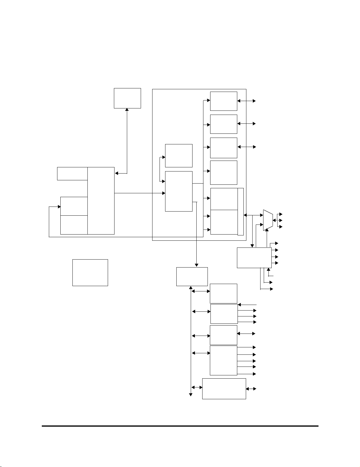
Freescale Semiconductor, Inc.
MCF5249 Block Diagram
• 1.8V core, 3.3V I/O
• 160 pin MAPBGA package (qualified at 140 MHz) and 144 pin QFP package (qualified at 120 MHz)
1.3 MCF5249 BLOCK DIAGRAM
nc...
I
cale Semiconductor,
Frees
Instruction
Cache
64K
SRAM1
32K
SRAM0
ColdFire
V2 Core
(160 BGA
140 Mhz)
(144 QFP
120 Mhz)
Clock
Multiplied
PLL
Debug
Module w/
JTAG
Standard ColdFire Peripheral Blocks
Timer
I2C
Dual
DMA
5x08
Arbiter
Translator
UART
5x08
Interrupt
S/DRAM
Interface
External
Bus
IDE
SmartMedia
Interrupt
Controller
QSPI
Interface
Audio
Interfaces
ADC
Flash Memory/
Card
Interface
Timer
Support
I2C
Interface
UART
Interface
MUX
(S)DRAM
SRAM
IDE
BUFEN1_B
BufEn_b1
BUFEN2_B
BufEn_b2
IDE-DIOR
IDE-DIOW
IDE-IORDY
SWE
SRE
QSPI_DIN
QSPI_Din
QSPI_DOUT
QSPI_Dout
QSPI_CS[3:0]
QSPI_CLK
Serial Audio
Interface
ebuin3_adin0_gpi38
EBUIN3/ADIN0_GP138
ebuin4_adin1_gpi39
EBUIN4/ADIN1_GP139
rxd2_adin2_gpi28
RXD2/ADIN2/GP128
CTS2/ADIN3/GP131
cts2_adin3_gpi31
TOUT1/ADOUT/GP135
tout1_adout_gpi35
MemoryStick/
SecureDigital
Interface
Figure 1-1 MCF5249 Block Diagram
1-2 MCF5249UM MOTOROLA
For More Information On This Product,
Go to: www.freescale.com

nc...
I
cale Semiconductor,
Frees
Freescale Semiconductor, Inc.
1.4 MCF5249 FEATURE DETAILS
The primary features of the MCF5249 integrated processor include the following:
• ColdFire V2 Processor Core operating at 140MHz
— Clock-doubled Version 2 microprocessor core
— 32-bit internal data bus, 16 bit external data bus
— 16 user-visible, 32-bit general-purpose registers
— Supervisor/user modes for system protection
— Vector base register to relocate exception-vector table
— Optimized for high-level language constructs
•DMA controller
— Four fully programmable channels: Two dedicated to the audio interface module and two
dedicated to the UART module (External requests are not supported.)
— Supports dual- and single-address transfers with 32-bit data capability
— Two address pointers that can increment or remain constant
— 16-/24-bit transfer counter
— Operand packing and unpacking support
— Auto-alignment transfers supported for efficient block movement
— Supports bursting and cycle stealing
— All channels support memory to memory transfers
— Interrupt capability
— Provides two clock cycle internal access
• Enhanced Multiply-accumulator Unit
— Single-cycle multiply-accumulate operations for 32 x 32 bit and 16 x 16 bit operands
— Support for signed, unsigned, integer, and fixed-point fractional input operands
— Four 48-bit accumulators to allow the use of a 40-bit product
— The addition of 8 extension bits to increase the dynamic number range
— Fast signed and unsigned integer multiplies
• 8-KByte Direct Mapped instruction cache
— Clocked at core clock frequency
— Flush capability
— Non-blocking cache provides fast access to critical code and data
• 96-KByte SRAM
— Provides one-cycle access to critical code and data
— Split into two banks, SRAM0 (32K), and SRAM1 (64K)
— DMA requests to/from internal SRAM1 supported
MCF5249 Feature Details
• Crystal Trim
— The XTRIM output can be used to trim an external crystal oscillator circuit which would allow
lock with an incoming IEC958 or serial audio signal
• Audio Interfaces
— IEC958 input and output
— Four serial Philips IIS/Sony EIAJ interfaces
– One with input and output, one with output only, two with input only (Three inputs, two outputs)
– Master and Slave operation
MOTOROLA Introduction 1-3
For More Information On This Product,
Go to: www.freescale.com

Freescale Semiconductor, Inc.
MCF5249 Feature Details
• CD Text Interface
— Allows the interface of CD subcode (transmitter only)
• Dual Universal Synchronous/Asynchronous Receiver/Transmitter (Dual UART)
— Full duplex operation
— Baud-rate generator
— Modem control signals: clear-to-send (CTS) and request-to-send (RTS)
— DMA interrupt capability
— Processor-interrupt capability
• Queued Serial Peripheral Interface (QSPI)
— Programmable queue to support up to 16 transfers without user intervention
— Supports transfer sizes of 8 to 16 bits in 1-bit increments
— Four peripheral chip-select lines for control of up to 15 devices
— Baud rates from 273 Kbps to 15 Mbps at 140MHz
— Programmable delays before and after transfers
nc...
I
— Programmable clock phase and polarity
— Supports wraparound mode for continuous transfers
— Master mode only
cale Semiconductor,
Frees
• Dual 16-bit General-purpose Multimode Timers
— Clock source selectable from external, CPU clock/2 and CPU clock/32.
— 8-bit programmable prescaler
— 2 timer inputs and 2 outputs
— Processor-interrupt capability
— 14.3 nS resolution with CPU clock at 140MHz
• IDE/ SmartMedia Interface
— Allows direct connection to an IDE hard drive or other IDE peripheral
• Analog/Digital Converter
— 12-Bit Resolution
— 4 Muxed inputs
• Flash Memory Card Interface
— Allows connection to Sony MemoryStick compatible devices
— Support SD cards and other types of flash media
•Dual I
• System debug support
2
C Interfaces
— Interchip bus interface for EEPROMs, LCD controllers, A/D converters, keypads
— Master and slave modes, support for multiple masters
— Automatic interrupt generation with programmable level
— Real-time instruction trace for determining dynamic execution path
— Background debug mode (BDM) for debug features while halted
— Debug exception processing capability
— Real-time debug support
1-4 MCF5249UM MOTOROLA
For More Information On This Product,
Go to: www.freescale.com

Freescale Semiconductor, Inc.
• System Interface
— Glueless bus interface and DRAMC support for interface to 16-bit for DRAM, SRAM, ROM,
FLASH, and I/O devices
— Two programmable chip-select signals for static memories or peripherals with programmable
wait states and port sizes.
— Two dedicated chip selects for 16-bit wide DRAM/SDRAM.
— CS0 is active after reset to provide boot-up from external FLASH/ROM.
— Two dedicated chip selects (CS2 and CS3) are used for the IDE and/or SmartMedia interface
— Programmable interrupt controller (low interrupt latency, eight external interrupt requests,
programmable autovector generator)
— 44 programmable general-purpose inputs (for the 160 MAPBGA package)
— 46 programmable general-purpose outputs (for the 160 MAPBGA package)
— IEEE 1149.1 Test (JTAG) Module
• Clocking
— Clock-multiplied PLL, programmable frequency
nc...
I
• 1.8V Core, 3.3V I/O
• 160 pin MAPBGA package (qualified at 140 MHz) and 144 pin QFP package (qualified at 120 MHz)
160 MAPBGA Ball Assignments
cale Semiconductor,
Frees
1.5 160 MAPBGA BALL ASSIGNMENTS
The following signals are not available on the 144 QFP package.
Table 1-1 160 MAPBGA Ball Assignments
160 MAPBGA BALL NUMBER FUNCTION GPIO
E3 CMD_SDIO2 GPIO34
G4 SDATA0_SDIO1 GPIO54
H3 RSTO/SDATA2_BS2
K3 A25 GPIO8
L4 QSPI_CS1 GPIO24
L8 QSPI_CS3 GPIO22
N8 SDRAM_CS2 GPIO7
P9 EBUOUT2 GPO 37
K11 BUFENB2 GPIO17
G12 SUBR GPIO 53
F13 SFSY GPIO 52
F12 RCK GPIO 51
E8 SRE GPIO11
B8 LRCK3 GPIO 45
E7 SWE GPIO12
A7 SCLK3 GPIO 49
MOTOROLA Introduction 1-5
For More Information On This Product,
Go to: www.freescale.com

Freescale Semiconductor, Inc.
MCF5249 Functional Overview
1.6 MCF5249 FUNCTIONAL OVERVIEW
1.6.1 COLDFIRE V2 CORE
The ColdFire processor Version 2 core consists of two independent, decoupled pipeline structures to
maximize performance while minimizing core size.The instruction fetch pipeline (IFP) is a two-stage
pipeline for prefetching instructions. The prefetched instruction stream is then gated into the two-stage
operand execution pipeline (OEP), which decodes the instruction, fetches the required operands, and then
executes the required function. Because the IFP and OEP pipelines are decoupled by an instruction buffer
that serves as a FIFO queue, the IFP can prefetch instructions in advance of their actual use by the OEP,
which minimizes time stalled waiting for instructions. The OEP is implemented in a two-stage pipeline
featuring a traditional RISC data path with a dual-read-ported register file feeding an arithmetic/logic unit
(ALU).
1.6.2 DMA CONTROLLER
The MCF5249 provides four fully programmable DMA channels for quick data transfer. Single and dual
nc...
I
address mode is supported with the ability to program bursting and cycle stealing. Data transfer is
selectable as 8, 16, 32, or 128-bits. Packing and unpacking is supported.
cale Semiconductor,
Frees
Two internal audio channels and the dual UART can be used with the DMA channels. All channels can
perform memory to memory transfers. The DMA controller has a user-selectable, 24- or 16-bit counter and
a programmable DMA exception handler.
External requests are not supported.
1.6.3 ENHANCED MULTIPLY AND ACCUMULATE MODULE (EMAC)
The integrated EMAC unit provides a common set of DSP operations and enhances the integer multiply
instructions in the ColdFire architecture. The EMAC provides functionality in three related areas:
1. Faster signed and unsigned integer multiplies
2. New multiply-accumulate operations supporting signed and unsigned operands
3. New miscellaneous register operations
Multiplies of 16x16 and 32x32 with 48-bit accumulates are supported in addition to a full set of extensions
for signed and unsigned integers plus signed, fixed-point fractional input operands. The EMAC has a
single-clock issue for 32x32-bit multiplication instructions and implements a four-stage execution pipeline.
1.6.4 INSTRUCTION CACHE
The instruction cache improves system performance by providing cached instructions to the execution unit
in a single clock. The MCF5249 processor uses a 8K-byte, direct-mapped instruction cache to achieve 125
MIPS at 140 Mhz. The cache is accessed by physical addresses, where each 16-byte line consists of an
address tag and a valid bit. The instruction cache also includes a bursting interface for 16-bit and 8-bit port
sizes to quickly fill cache lines.
1.6.5 INTERNAL 96-KBYTE SRAM
The 96-KByte on-chip SRAM is split over two banks, SRAM0 (64k) and SRAM1 (32K). It provides one
clock-cycle access for the ColdFire core. This SRAM can store processor stack and critical code or data
segments to maximize performance. Memory in the second bank can be accessed under DMA.
1-6 MCF5249UM MOTOROLA
For More Information On This Product,
Go to: www.freescale.com

Freescale Semiconductor, Inc.
MCF5249 Functional Overview
1.6.6 DRAM CONTROLLER
The MCF5249 DRAM controller provides a glueless interface for up to two banks of DRAM, each of which
can be up to 32 MBytes. The controller supports a 16-bit data bus. A unique addressing scheme allows for
increases in system memory size without rerouting address lines and rewiring boards. The controller
operates in page mode, non-page mode, and burst-page mode and supports SDRAMs.
1.6.7 SYSTEM INTERFACE
The MCF5249 provides a glueless interface to 16-bit port size SRAM, ROM, and peripheral devices with
independent programmable control of the assertion and negation of chip-select and write-enable signals.
The MCF5249 also supports bursting ROMs.
1.6.8 EXTERNAL BUS INTERFACE
The bus interface controller transfers information between the ColdFire core or DMA and memory,
peripherals, or other devices on the external bus. The external bus interface provides 23 bits of address
nc...
I
bus space, a 16-bit data bus, Output Enable, and Read/Write signals. This interface implements an
extended synchronous protocol that supports bursting operations.
cale Semiconductor,
Frees
1.6.9 SERIAL AUDIO INTERFACES
The MCF5249 digital audio interface provides four serial Philips IIS/Sony EIAJ interfaces. One interface is
a 4-pin (1 bit clock, 1 word clock, 1 data in, 1 data out), the other three interfaces are 3-pin (1 bit clock, 1
word clock, 1 data in or out). The serial interfaces have no limit on minimum sampling frequency.
Maximum sampling frequency is determined by the maximum frequency on the bit clock input. (1/3 the
frequency of the internal system clock.)
1.6.10 IEC958 DIGITAL AUDIO INTERFACES
The MCF5249 has two digital audio input interfaces, and one digital audio output interface. There are four
digital audio input pins and two digital audio output pins. An internal multiplexer selects one of the four
inputs to the digital audio input interface.
There is one digital audio output interface with two IEC958 outputs. One output carries the professional “c”
channel (Channel Status), and the other carries the consumer “c” channel. All other bits (audio data, user
channel bits, validity flag, etc) are identical.
The IEC958 output can take the output from the internal IEC958 generator, or multiplex out one of the four
IEC958 inputs.
1.6.11 AUDIO BUS
The audio interfaces connect to an internal bus that carries all audio data. Each receiver places its
received data on the audio bus and each transmitter takes data from the audio bus for transmission. Each
transmitter has a source select register.
In addition to the audio interfaces, there are six CPU accessible registers connected to the audio bus.
Three of these registers allow data reads from the audio bus and allow selection of the audio source. The
other three registers provide a write path to the audio bus and can be selected by transmitters as the audio
source. Through these registers, the CPU has access to the audio samples for processing.
MOTOROLA Introduction 1-7
For More Information On This Product,
Go to: www.freescale.com

Freescale Semiconductor, Inc.
MCF5249 Functional Overview
Audio can be routed from a receiver to a transmitter without the data being processed by the core so the
audio bus can be used as a digital audio data switch. The audio bus can also be used for audio format
conversion.
1.6.12 CD-ROM ENCODER/DECODER
The MCF5249 is capable of processing CD-ROM sectors in hardware. Processing is compliant with
CD-ROM and CD-ROM XA standards.
The CD-ROM decoder performs following functions in hardware:
• Sector sync recognition
• Descrambling of sectors
• Verification of the CRC checksum for Mode 1, Mode 2 Form 1, and Mode 2 Form 2 sectors
• Third-layer error correction is not performed
The CD-ROM encoder performs following functions in hardware:
nc...
I
cale Semiconductor,
Frees
• Sector sync recognition
• Scrambling of sectors
• Insertion of the CRC checksum for Mode 1, Mode 2 Form 1, and Mode 2 Form 2 sectors.
• Third-layer error encoding needs to be done in software. This can use approximately 5-10 Mhz of
performance for single-speed.
1.6.13 DUAL UART MODULE
Two full-duplex UARTs with independent receive and transmit buffers are in this module. Data formats can
be 5, 6, 7, or 8 bits with even, odd, or no parity, and up to 2 stop bits in 1/16 increments. Four-byte receive
buffers and two-byte transmit buffers minimize CPU service calls. The Dual UART module also provides
several error-detection and maskable-interrupt capabilities. Modem support includes request-to-send
) and clear-to-send (CTS) lines.
(RTS
The system clock provides the clocking function from a programmable prescaler. Users can select full
duplex, auto-echo loopback, local loopback, and remote loopback modes. The programmable Dual UARTs
can interrupt the CPU on various normal or error-condition events.
1.6.14 QUEUED SERIAL PERIPHERAL INTERFACE QSPI
The QSPI module provides a serial peripheral interface with queued transfer capability. It supports up to 16
stacked transfers at a time, making CPU intervention between transfers unnecessary. Transfers of up to
17.5 Mbits/second are possible at a CPU clock of 140 MHz. The QSPI supports master mode operation
only.
1.6.15 TIMER MODULE
The timer module includes two general-purpose timers, each of which contains a free-running 16-bit timer
for use in any of three modes:
1. Input Capture. This mode captures the timer value with an external event.
2. Output Compare. This mode triggers an external signal or interrupts the CPU when the timer
reaches a set value
3. Event Counter. This mode counts external events.
1-8 MCF5249UM MOTOROLA
For More Information On This Product,
Go to: www.freescale.com

Freescale Semiconductor, Inc.
The timer unit has an 8-bit prescaler that allows programming of the clock input frequency, which is
derived from the system clock. In addition to the ÷1 and ÷16 clock derived from the bus clock (CPU clock /
2), the programmable timer-output pins either generate an active-low pulse or toggle the outputs.
MCF5249 Functional Overview
1.6.16 IDE AND SMARTMEDIA INTERFACES
The MCF5249 system bus allows connection of an IDE hard disk drive and SmartMedia flash card with a
minimum of external hardware. The external hardware consists of bus buffers for address and data and
are intended to reduce the load on the bus and prevent SDRAM and Flash accesses to propagate to the
IDE bus. The control signals for the buffers are generated in the MCF5249.
1.6.17 ANALOG/DIGITAL CONVERTER (ADC)
The four channel ADC is based on the Sigma-Delta concept with 12-bit resolution. The digital portion of the
ADC is provided internally. The analog voltage comparator must be provided externally as well as an
external integrator circuit (resistor/capacitor) which is driven by the ADC output. A software interrupt is
provided when the ADC measurement cycle is complete.
nc...
I
1.6.18 FLASH MEMORY CARD INTERFACE
cale Semiconductor,
Frees
The interface is Sony MemoryStick and SecureDigital compatible. However, there is no hardware support
for MagicGate
™.
1.6.19 I2C MODULE
The two-wire I2C bus interface, which is compliant with the Philips I2C bus standard, is a bidirectional serial
bus that exchanges data between devices. The I
the end system and is best suited for applications that need occasional bursts of rapid communication over
short distances among several devices. Bus capacitance and the number of unique addresses limit the
maximum communication length and the number of devices that can be connected.
2
C bus minimizes the interconnection between devices in
1.6.20 CHIP-SELECTS
There are four programmable chip selects on the MCF5249:
• Two programmable chip-select outputs (CS0 and CS1) provide signals that enable glueless
connection to external memory and peripheral circuits. The base address, access permissions, and
automatic wait-state insertion are programmable with configuration registers. These signals also
interface to 16-bit ports.
• Two dedicated chip selects (CS2 and CS3) are used for the IDE and/or SmartMedia interface
CS0 is active after reset to provide boot-up from external FLASH/ROM.
1.6.21 GPIO INTERFACE
A total of 44 General Purpose inputs and 46 General Purpose outputs are available. These are multiplexed
with various other signals. Eight of the GPIO inputs have edge sensitive interrupt capability.
1.6.22 INTERRUPT CONTROLLER
The MCF5249 has a primary and a secondary interrupt controller. These interrupt controllers handle
interrupts from all internal interrupt sources. In addition, there are 8 GPIOs where external interrupts can
MOTOROLA Introduction 1-9
For More Information On This Product,
Go to: www.freescale.com

Freescale Semiconductor, Inc.
MCF5249 Functional Overview
be generated on the rising or falling edge of the pin. All interrupts are autovectored and interrupt levels are
programmable.
1.6.23 JTAG
To help with system diagnostics and manufacturing testing, the MCF5249 includes dedicated
user-accessible test logic that complies with the IEEE 1149.1A standard for boundary scan testability,
often referred to as Joint Test Action Group, or JTAG. For more information, refer to the IEEE 1149.1A
standard. Motorola provides BSDL files for JTAG testing.
1.6.24 SYSTEM DEBUG INTERFACE
The ColdFire processor core debug interface supports real-time instruction trace and debug, plus
background-debug mode. A background-debug mode (BDM) interface provides system debug.
In real-time instruction trace, four status lines provide information on processor activity in real time (PST
pins). A four-bit wide debug data bus (DDATA) displays operand data and change-of-flow addresses,
nc...
I
which helps track the machine’s dynamic execution path.
1.6.25 CRYSTAL AND ON-CHIP PLL
cale Semiconductor,
Frees
Typically, an external 16.92 Mhz or 33.86 Mhz clock input is used for CD R/W applications, while an
11.2896 MHz clock is more practical for Portable CD player applications. However, the on-chip
programmable PLL, which generates the processor clock, allows the use of almost any low frequency
external clock (5-35 Mhz).
Two clock outputs (MCLK1 and MCLK2) are provided for use as Audio Master Clock. The output
frequencies of both outputs are programmable to Fxtal, Fxtal/2, Fxtal/3, and Fxtal/4. The Fxtal/3 option is
only available when the 33.86 Mhz crystal is connected.
The MCF5249 supports VCO operation of the oscillator by means of a 16-bit pulse density modulation
output. Using this mode, it is possible to lock the oscillator to the frequency of an incoming IEC958 or IIS
signal. The maximum trim depends on the type and design of the oscillator. Typically a trim of +/- 100 ppm
can be achieved with a crystal oscillator and over +/- 1000 ppm with an LC oscillator.
1-10 MCF5249UM MOTOROLA
For More Information On This Product,
Go to: www.freescale.com

Freescale Semiconductor, Inc.
Section 2 Signal Description
2.1 INTRODUCTION
This section describes the MCF5249 input and output signals. The signal descriptions as shown in Table
2-1 are grouped according to relevant functionality.
Table 2-1 MCF5249 Signal Index
nc...
I
cale Semiconductor,
Frees
SIGNAL NAME MNEMONIC FUNCTION
Address A[23:1]
A[25]/GPO8
Read-write control RW_b Bus write enable - indicates if read or
Output enable OE Output enable for asynchronous
Data D[31:16] Data bus used to transfer word data In/Out Hi-Z
Synchronous row address
strobe
Synchronous column
address strobe
SDRAM write enable SDWE Write enable for external SDRAM Out negated
SDRAM upper byte
enable
SDRAM lower byte enable SDLDQM Indicates during write cycle if low
SDRAM chip selects SDRAMCS1 SDRAM chip select Out negated
SDRAM chip selects SDRAMCS2/GPIO7 SDRAM chip select In/Out negated
SDRAM clock enable BCLKE SDRAM clock enable Out
System clock SCLK/GPIO10 SDRAM clock output In/Out
ISA bus read strobes CS2/IDE-DIOR/GPIO13
ISA bus write strobes IDE-DIOW/GPIO14
ISA bus wait signal IDE-IORDY/GPIO16 ISA bus wait line - available for both
Chip Selects[1:0] CS0
Buffer enable 1 BUFENB1
Buffer enable 2 BUFENB2
Transfer acknowledge TA/GPIO20 Transfer Acknowledge signal In/Out
SDRAS Row address strobe for external
SDCAS Column address strobe for external
SDUDQM Indicates during write cycle if high
CS3/SRE/GPIO11
SWE/GPIO12
CS1/GPIO58
/GPIO57 Two programmable buffer enables
/GPIO7 In/Out
23 address bus lines, address line 25
multiplexed with gpo8
write cycle in progress
memories connected to chip selects
SDRAM.
SDRAM
byte is written
byte is written
There are 2 ISA bus read strobes
and 2 ISA bus write strobes. They
Allow connection of two independent
ISA bus peripherals, e.g. an IDE
slave device and a SmartMedia card
busses
Enables peripherals at programmed
addresses. CS[1:0]. CS[0] provides
boot ROM selection
Allow seamless steering of external
buffers to split data and address bus
in sections.
INPUT/
OUTPUT
Out X
Out H
Out negated
Out negated
Out negated
Out
Out
In/Out
In/Out
In/Out
Out
In/Out
In/Out
RESET
STATE
negated
MOTOROLA Signal Description 2-1
For More Information On This Product,
Go to: www.freescale.com

Introduction
Freescale Semiconductor, Inc.
Table 2-1 MCF5249 Signal Index (Continued)
nc...
I
cale Semiconductor,
Frees
SIGNAL NAME MNEMONIC FUNCTION
Serial Clock line SCL0/QSPI_CLK
Serial Data Line SDA0/QSPI_DIN
Serial Clock Line SCL1_GPIO3
Serial Data Line SDA1_GPIO55
Receive Data RXD1/GPI28/ADIN2
RXD0/GPI27
Transmit Data TXD1/GPO28
TXD0/GPO27
Request-To-Send RTS
Clear-To-Send CTS
Timer Input TIN0/GPI33
Timer Output TOUT0/GPO33
IEC958 inputs EBUIN1/GPI36
IEC958 outputs EBUOUT1/GPO36
Serial data in SDATAI1
Serial data out SDATAO1/GPIO25
Word clock LRCK1
Bit clock SCLK1
Serial input EF/GPIO19 Error flag serial in In/Out
Serial input CFLG/GPIO18 C-flag serial in In/Out
1/GPO31
RTS
2/GPO30
1/ADIN3/GPI31
0/GPI30
CTS
TIN1/GPIO23
TOUT1/ADOUT/GPO35
EBUIN2/GPI37
EBUIN3/ADIN0/GPI38
EBUIN4/ADIN1/GPI39
EBUOUT2/GPO37
SDATAI3/GPI41
SDATAI4/GPI42
SDATAO2/GPO41
LRCK2/GPIO44
LRCK3/GPIO45
LRCK4/GPIO46
SCLK2/GPIO48
SCLK3/GPIO49
SCLK4/GPIO50
Clock signal for first I
operation
Signal is also QSPI clock
Serial data port first I
operation
Signal is also QSPI data in
Clock signal for second I
operation
Serial data port for second I
module operation
Signal is receive serial data input for
DUART
Signal is transmit serial data output
for DUART
DUART signals a ready to receive
data query
Signals to DUART that data can be
transmitted to peripheral
2 is multiplexed with an A/D
CTS
input
Provides clock input to timer or
provides trigger to timer value
capture logic
Capable of output waveform or pulse
generation
Audio interfaces IEC958 inputs
multiplexed with some A/D inputs
Audio interfaces IEC958 outputs Out
Audio interfaces serial data inputs In
Audio interfaces serial data outputs In/Out
Audio interfaces serial word clocks In/Out
Audio interfaces serial bit clocks In/Out
2
C module
2
C module
2
C module
2
C
INPUT/
OUTPUT
In/Out
In/Out
In/Out
In/Out
In
Out asserted
Out negated
In
In
In/Out
Out
In
Out
RESET
STATE
2-2 MCF5249UM MOTOROLA
For More Information On This Product,
Go to: www.freescale.com

Freescale Semiconductor, Inc.
Table 2-1 MCF5249 Signal Index (Continued)
Introduction
nc...
I
cale Semiconductor,
Frees
SIGNAL NAME MNEMONIC FUNCTION
Subcode clock RCK/GPIO51 Audio interfaces subcode clock In/Out
Subcode sync SFSY/GPIO52 Audio interfaces subcode sync In/Out
Subcode data SUBR/GPIO53 Audio interfaces subcode data In/Out
Clock frequency trim XTRIM/GPO38 Clock trim control Out
Audio clocks out MCLK1/GPO39
MCLK2/GPO42
MemoryStick/Secure
Digital interface
ADC EBUIN3/ADIN0/GPI38
ADC TOUT1/ADOUT/GPO35 Analog to digital convertor output
QSPI clock SCL/QSPI_CLK QSPI clock signal In/Out
QSPI data in SDA/QSPI_DIN QSPI data input In/Out
QSPI data out QSPIDOUT/GPIO26 QSPI data out In/Out
QSPI chip selects QSPICS0/GPIO29
Crystal in CRIN Crystal input In
Reset In RSTI Processor Reset Input In
Motorola Test Mode TEST[3:0] Should always be low. In
High Impedance HIZ Assertion three-states all output
Debug Data DDATA3/GPIO4
Processor Status PST3/GPIO62
Processor clock PSTCLK/GPO63 Processor clock output Out
CMDSDIO2/GPIO34 Secure Digital command lane
SCLKOUT/GPIO15 Clock out for both MemoryStick
SDATA0_SDIO1/GPIO54 SecureDigital serial data bit 0
SDATA1_BS1/GPIO9 SecureDigital serial data bit 1
RSTO/SDATA2_BS2 SecureDigital serial data bit 2
SDATA3/GPIO56 SecureDigital serial data bit 3 In/Out
EBUIN4/ADIN1/GPI39
RXD2/ADIN2/GPI28
CTS2/ADIN3/GPI31
QSPICS1/GPIO24
QSPICS2/GPIO21
QSPICS3/GPIO22
DDATA2/GPIO2
DDATA1/GPIO1
DDATA0/GPIO0
PST2/GPIO61
PST1/GPIO60
PST0/GPIO59
DAC output clocks Out
MemoryStick interface 2 data i/o
interfaces and for Secure Digital
MemoryStick interface 1 data i/o
MemoryStick interface 1 strobe
MemoryStick interface 2 strobe
Reset output signal
Analog to Digital converter input
signals
signal
QSPI chip selects In/Out
signal pins.
Displays captured processor data
and break-point status.
Indicates internal processor status. In/Out Hi-Z
INPUT/
OUTPUT
In/Out
In/Out
In/Out
In/Out
In/Out
In/Out
In/Out
In
In/Out Hi-Z
RESET
STATE
MOTOROLA Signal Description 2-3
For More Information On This Product,
Go to: www.freescale.com

GPIO
Freescale Semiconductor, Inc.
Table 2-1 MCF5249 Signal Index (Continued)
nc...
I
cale Semiconductor,
Frees
SIGNAL NAME MNEMONIC FUNCTION
Test Clock TCK Clock signal for IEEE 1149.1A JTAG. In
Test Reset/Development
Serial Clock
Test Mode Select/ Break
Point
Test Data Input /
Development Serial Input
Test Data
Output/Development
Serial Output
Note: The CMD_SDIO2, SDATA0_SDIO1, RSTO/SDATA2_BS2, A25, QSPI_CS1,
QSPI_CS3, SDRAM_CS2, EBUOUT2, BUFENB2, SUBR, SFSY, RCK, SRE,
LRCK3, SWE, and the SCLK3 signals are only used in the 160 MAPBGA package.
/DSCLK Multiplexed signal that is
TRST
asynchronous reset for JTAG
controller. Clock input for debug
module.
TMS/BKPT
TDI/DSI Multiplexed serial input for the JTAG
TDO/DSO Multiplexed serial output for the
Multiplexed signal that is test mode
select in JTAG mode and a hardware
break-point in debug mode.
or background debug module.
JTAG or background debug module.
INPUT/
OUTPUT
Out
In
In
In
RESET
STATE
2.2 GPIO
Many pins have a GPIO as first or second function. If gpio is second function, following rules apply:
• General purpose input is always active, regardless of state of pin.
• General purpose output or primary output is determined by value written to gpio function select
register.
• Power-on reset function is not gpio
2.3 MCF5249 BUS SIGNALS
These signals provide the external bus interface to the MCF5249.
2.3.1 ADDRESS BUS
• The address bus provides the address of the byte or most significant byte of the word or longword
being transferred.The address lines also serve as the DRAM address pins, providing multiplexed row
and column address signals.
• Bits 23 down to 1 and 25 of the address are available. A25 is intended to be used with 256 Mbit
DRAM’s. Signals are named:
•A[23:1]
• A[25]/GPO8
2.3.2 READ-WRITE CONTROL
This signal indicates during any bus cycle whether a read or write is in progress. A low is write cycle and a
high is a read cycle.
2-4 MCF5249UM MOTOROLA
For More Information On This Product,
Go to: www.freescale.com

Freescale Semiconductor, Inc.
SDRAM Controller Signals
2.3.3 OUTPUT ENABLE
The OE signal is intended to be connected to the output enable of asynchronous memories connected to
chip selects. During bus read cycles, the ColdFire processor will drive OE
low.
2.3.4 DATA BUS
The data bus (D[31:16]) is bi-directional and non-multiplexed. Data is registered by the MCF5249 on the
rising clock edge. The port width for each chip-select and DRAM bank are programmable. The data bus
uses a default configuration if none of the chip-selects or DRAM bank match the address decode. All 16
bits of the data bus are driven during writes, regardless of port width or operand size.
2.3.5 TRANSFER ACKNOWLEDGE
The TA/GPIO20 pin is the transfer acknowledge signal.
2.4 SDRAM CONTROLLER SIGNALS
nc...
I
cale Semiconductor,
Frees
The following SDRAM signals provide a seamless interface to external SDRAM. An SDRAM width of 16
bits is supported and can access as much as 64 Mbytes of memory. ADRAMs are not supported.
Table 2-2 SDRAM Controller Signals
SDRAM SIGNAL DESCRIPTION
synchronous DRAM row address strobe The SDRAS
RAS input on synchronous DRAM
Synchronous DRAM Column Address
Strobe
Synchronous DRAM Write The SDWE
Synchronous DRAM Chip Enables The SDRAM_CS1
Synchronous DRAM UDQM and LQDM
signals
Synchronous DRAM clock The DRAM clock is driven by the SCLK signal
Synchronous DRAM Clock Enable The BCLKE active high output signal is used during
The SDCAS
CAS input on synchronous DRAM.
write cycle is underway. This pin outputs logic ‘1’ during read
bus cycles.
signals are used during synchronous mode to route directly to
the chip selects of up to 2 SDRAM devices.
The SDRAM_CS2
the GPIO-FUNCTION register.
The DRAM byte enables UDMQ and LDQM are driven by the
SDUDQM and SDLDQM byte enable outputs.
synchronous mode to route directly to the SCKE signal of
external SDRAMs. This signal provides the clock enable to the
SDRAM.
active low pin provides a seamless interface to the
active low pin provides a seamless interface to
active-low pin is asserted to signify that a SDRAM
and SDRAM_CS2/gpio7 active-low output
/gpio7 can be programmed to be gpio using
Note: The SDRAM_CS2 signal is only used on the 160 MAPBGA package.
2.5 CHIP SELECTS
There are two chip select outputs on the MCF5249 device. CS0 and CS1/GPIO58. The second signal is
multiplexed with a GPIO signal. The active low chip selects can be used to access asynchronous
memories. The interface is glueless.
MOTOROLA Signal Description 2-5
For More Information On This Product,
Go to: www.freescale.com

ISA bus
Freescale Semiconductor, Inc.
2.6 ISA BUS
The MCF5249 supports an ISA bus. (No ISA DMA channel). Using the ISA bus protocol, reads and writes
to up to two ISA bus peripherals are possible. For the first peripheral, CS2/IDE-DIOR/
IDE-DIOW
SWE
IDE-IORDY/GPIO16
/GPIO14 are the read and write strobe. For the second peripheral, CS3/SRE/GPIO11 and
/GPIO12 are the read and write strobe. Either peripheral can insert wait states by pulling
GPIO13 and
2.7 BUS BUFFER SIGNALS
As the MCF5249 has a quite complicated slave bus, with the possibility to put DRAM on the bus, put
asynchronous memories on the bus, and to put ISA bus peripherals on the bus, it may become necessary
to introduce a bus buffer on the bus. The MCF5249 has a glueless interface to steer these bus buffers with
2 bus buffer output signals BUFENB1
Note: The BUFENB2 signal is only used in the 160 MAPBGA package.
/GPIO57 and BUFENB2/GPIO7.
nc...
I
cale Semiconductor,
Frees
2.8 I2C MODULE SIGNALS
There are two I2C interfaces on this device.
2
The I
C module acts as a quick two-wire, bidirectional serial interface between the MCF5249 processor
and peripherals with an I
devices connected to the I
be accomplished with an open-drain output.
I2C MODULE SIGNAL DESCRIPTION
2
I
C Serial Clock
2
I
C Serial Data
2
C interface (e.g., LED controller, A-to-D converter, D-to-A converter). When
2
C bus drive the bus, they will either drive logic-0 or high-impedance. This can
Table 2-3 I2C Module Signals
The SCL/QPSICLK and SCL2/GPIO3 bidirectional signals are
the clock signal for first and second I
2
C module controls this signal when the bus is in master
I
2
mode; all I
timing.
Signals are multiplexed
Function select is done via PLLCR register.
The SDA/QSPI_DIN and SDA2/GPIO55 bidirectional signals
are the data input/output for the first and second serial I
interface.
Signals are multiplexed
Function select is done via PLLCR register.
C devices drive this signal to synchronize I2C
2
C module operation. The
2
C
2.9 SERIAL MODULE SIGNALS
The following signals transfer serial data between the two UART modules and external peripherals.
All serial module signals can be used as gpi or gpo. The GPIO-FUNCTION and GPIO1-FUNCTION
registers must be programmed to determine pin functions of the inputs and outputs. If used as gpo or gpi,
UART functionality is lost.
2-6 MCF5249UM MOTOROLA
For More Information On This Product,
Go to: www.freescale.com

Freescale Semiconductor, Inc.
SERIAL MODULE SIGNAL DESCRIPTION
Receive Data The RXD1_GPI27 and RXD2/ADIN2/GPI28 are the inputs on
Transmit Data The DUART transmits serial data on the TXD1/GPO27 and
Request To Send The RTS
nc...
I
Clear To Send Peripherals drive the CTS
Timer Module Signals
Table 2-4 Serial Module Signals
which serial data is received by the DUART. Data is sampled
on RxD[1:0] on the rising edge of the serial clock source, with
the least significant bit received first.
TXD2/GPO28 output signals. Data is transmitted on the falling
edge of the serial clock source, with the least significant bit
transmitted (LSB) first. When no data is being transmitted or
the transmitter is disabled, these two signals are held high.
TxD[1:0] are also held high in local loopback mode.
1/GPO30 and RTS2/GPO31 request-to-send outputs
indicate to the peripheral device that the DUART is ready to
send data and requires a clear-to-send signal to initiate
transfer.
1/GPI30 and CTS2/ADIN3/GPI31
inputs to indicate to the MCF5249 serial module that it can
begin data transmission.
cale Semiconductor,
Frees
2.10 TIMER MODULE SIGNALS
The following signals are external interface to the two general-purpose MCF5249 timers. These 16-bit
timers can capture timer values, trigger external events, or internal interrupts, or count external events.
These pins can be reused as GPO or GPI. Registers GPIO-FUNCTION and GPIO1-FUNCTION must be
programmed for this.
Table 2-5 Timer Module Signals
SERIAL MODULE SIGNAL DESCRIPTION
Timer Input Users can program the TIN0/GPI33 and TIN1/GPIO23 inputs
as clocks that cause events in the counter and prescalars.
They can also cause capture on the rising edge, falling edge,
or both edges.
Timer Output The TOUT0/GPO33 and TOUT1/ADOUT/GPO35
programmable outputs pulse or toggle on various timer events.
2.11 SERIAL AUDIO INTERFACE SIGNALS
All serial audio interface signals can be programmed to serve as general purpose I/Os or as serial audio
interface signals. The function is programmed using GPIO-FUNCTION and GPIO1-FUNCTION registers.
Note: The LRCK3 and SCLK3 signals are only used in the 160 MAPBGA package.
MOTOROLA Signal Description 2-7
For More Information On This Product,
Go to: www.freescale.com

nc...
I
cale Semiconductor,
Frees
Freescale Semiconductor, Inc.
Serial Audio Interface Signals
Table 2-6 Serial Audio Interface Signals
SERIAL MODULE SIGNAL DESCRIPTION
Serial Audio Bit Clock The SCLK1, SCLK2/GPIO48, SCLK3/GPIO49, AND
Serial Audio Word Clock The LRCK1, LRCK2/GPIO44, LRCK3/GPIO45, AND
Serial Audio Data In The SDATAI1, SDATAI3/GPI41, SDATAI4/GPI42 multiplexed
Serial Audio Data Out The SDATAO1/GPIO25 AND SDATAO2/GPI41 multiplexed
Serial audio error flag The EF/GPIO19 multiplexed pin can serve as general purpose
Serial audio CFLG The CFLG/GPIO18 multiplexed pin can serve as general
SCLK4/GPIO50 multiplexed pins can serve as general purpose
I/Os or serial audio bit clocks. As bit clocks, these bidirectional
pins can be programmed as outputs to drive their associated
serial audio (IIS) bit clocks. Alternately, these pins can be
programmed as inputs when the serial audio bit clocks are
driven internally. The functionality is programmed within the
Audio module. During reset, these pins are configured as input
serial audio bit clocks.
LRCK4/GPIO46 multiplexed pins can serve as general
purpose I/Os or serial audio word clocks. As word clocks, the
bidirectional pins can be programmed as inputs to drive their
associated serial audio word clock. Alternately, these pins can
be programmed as outputs when the serial audio word clocks
are derived internally. The functionality is programmed within
the Audio module. During reset, these pins are configured as
input serial audio word clocks.
pins can serve as general purpose I/Os or serial audio inputs.
As serial audio inputs the data is sent to interfaces 1,3 and 4
respectively. The functionality of these pins is programmed
with the GPIO-FUNCTION and GPIO1-FUNCTION registers.
During reset, the pins are configured as serial data inputs.
pins can serve as general purpose I/Os or serial audio outputs.
The functionality of these pins is programmed with registers
GPIO-FUNCTION and GPIO1-FUNCTION. During reset, the
pins are configured as serial data outputs.
I/Os or error flag input. As error flag input, this pin will input the
error flag delivered by the CD-DSP. EF/GPIO19 is only
relevant for serial interface in 1
purpose I/O or CFLG input. As CFLG input, the pin will input
the CFLG flag delivered by the CD-DSP. CFLG/GPIO18 is only
relevant for serial interface in 1.
2-8 MCF5249UM MOTOROLA
For More Information On This Product,
Go to: www.freescale.com

Freescale Semiconductor, Inc.
Digital Audio Interface Signals
2.12 DIGITAL AUDIO INTERFACE SIGNALS
Table 2-7 Digital Audio Interface Signals
SERIAL MODULE SIGNAL DESCRIPTION
Digital Audio In The EBUIN1/GPI36, EBUIN2/GPI37, EBUIN3/ADIN0/GPI38,
and EBUIN4/ADIN1/GPI39 multiplexed signals can serve as
general purpose input or can be driven by various digital audio
(IEC958) input sources. Both functionalities are always active.
Input chosen for IEC958 receiver is programmed within the
audio module. Input value on the 4 pins can always be read
from the appropriate gpio register.
Digital Audio Out The EBUOUT1_GPO36 and EBUOUT2_GPO37 multiplexed
pins can serve as general purpose I/O or as digital audio
(IEC958) output. EBUOUT1 is digital audio out for consumer
mode, EBUOUT2 is digital audio out for professional mode.
The functionality of the pins is programmed with the
nc...
I
GPIO-FUNCTION and GPIO1-FUNCTION register. During
reset, the pin is configured as a digital audio output.
cale Semiconductor,
Frees
Note: The EBUOUT2 signal is only used on the 160 MAPBGA package.
2.13 SUBCODE INTERFACE
There is a 3-line subcode interface on the MCF5249. This 3-line subcode interface allows the device to
format and transmit subcode in EIAJ format to a CD channel encoder device. The three signals are
described in Table 2-8
Table 2-8 Subcode Interface Signal
SIGNAL NAME DESCRIPTION
RCK/GPIO51 Subcode clock input. When pin is used as subcode clock, this
pin is driven by the CD channel encoder.
SFSY/GPIO52 Subcode sync output
This signal is driven high if a subcode sync needs to be
inserted in the EFM stream.
SUBR/GPIO53 Subcode data output
This signal is a subcode data out pin.
Note: The SUBR, SFSY, and the RCK signals are only used in the 160 MAPBGA
package.
2.14 ANALOG TO DIGITAL CONVERTER (ADC)
The single output on the TOUT1/ADOUT/GPO35 pin provides the reference voltage in PDM format
therefore this output requires an external integrator circuit (resistor/capacitor) to convert it to a DC level to
be used by the external comparator circuit.
Four external comparators compare the DC level obtained after filtering TOUT1/ADOUT/GPO35 with the
relevant input signals. The outputs of the comparators are fed to the 4 ADIN inputs on the MCF5249:
EBUIN3/ADIN0/GPI38, EBUIN4/ADIN1/GPI39, RXD2/ADIN2/GPI38 and CTS2/ADIN3/GPI31.
MOTOROLA Signal Description 2-9
For More Information On This Product,
Go to: www.freescale.com

nc...
I
cale Semiconductor,
Frees
Freescale Semiconductor, Inc.
Secure Digital/ MemoryStick card Interface
Selection of function for pin TOUT1/ADOUT/GPO35 is done by writing GPIO function select register
(determines if function is GPIO or not), and differentiation between timer and adout functions is done in the
ADCONFIG Register.
2.15 SECURE DIGITAL/ MEMORYSTICK CARD INTERFACE
The device has a versatile flash card interface that supports both SecureDigital and MemoryStick cards.
The interface can either support one SecureDigital or two MemoryStick cards. No mixing of card types is
possible. Table 2-9 gives the pin descriptions.
Table 2-9 Flash Memory Card Signals
FLASH MEMORY SIGNAL DESCRIPTION
SCLKOUT/GPIO15 Clock out for both MemoryStick interfaces and for
SecureDigital
CMD_SDIO2/GPIO34 Secure Digital command line
MemoryStick interface 2 data i/o
SDATA0_SDIO1/GPIO54 SecureDigital serial data bit 0
MemoryStick interface 1 data i/o
SDATA1_BS1/GPIO9 SecureDigital serial data bit 1
MemoryStick interface 1 strobe
RSTO/SDATA2_BS2 SecureDigital serial data bit 2
MemoryStick interface 2 strobe
Reset output signal
Selection between Reset function and SDATA2_BS2 is done
by programming PLLCR register.
SDATA3/GPIO57 SecureDigital serial data bit 3
Note: The SDATA0_SDIO1 and RSTO/SDATA2_BS2 signals are only used in the 160
MAPBGA package.
2.16 QUEUED SERIAL PERIPHERAL INTERFACE (QSPI)
Table 2-10 Queued Serial Peripheral Interface (QSPI) Signals
SERIAL MODULE SIGNAL DESCRIPTION
SCL_QSPICLK Multiplexed signal IIC interface clock or QSPI clock output
Function select is done via PLLCR register.
SDA_QSPIDIN Multiplexed signal IIC interface data or QSPI data input.
Function select is done via PLLCR register.
QSPIDOUT_GPIO26 QSPI data output
QSPICS0_GPIO29 4 different QSPI chip selects
QSPICS1_GPIO24
QSPICS2_GPIO21
QSPICS3_GPIO22
Note: The CMD_SDIO2 signal is only used in the 160 MAPBGA package.
The QSPI interface is a high-speed serial interface allowing transmit and receive of serial data. Pin
descriptions are given in Table 2-10.
2-10 MCF5249UM MOTOROLA
For More Information On This Product,
Go to: www.freescale.com

Freescale Semiconductor, Inc.
Crystal Trim
2.17 CRYSTAL TRIM
The XTRIM_GPO38 output produces a pulse-density modulated phase/frequency difference signal to be
used after low-pass filtering to control varicap-voltage to control crystal oscillation frequency. This will lock
the crystal to the incoming digital audio signal.
2.18 CLOCK OUT
The MCLK1/GPO39 and MCLK2/GPO42 can serve as general purpose I/Os or as DAC clock outputs.
When programmed as DAC clock outputs, these signals are directly divided from the crystal.
2.19 DEBUG AND TEST SIGNALS
These signals interface with external I/O to provide processor status signals.
2.19.1 TEST MODE
The TEST[3:0] inputs are used for various manufacturing and debug tests. For normal mode these inputs
nc...
I
should always be tied low. Use TEST0 to switch between background debug mode and JTAG mode. Drive
TEST0 high for debug mode.
cale Semiconductor,
Frees
2.19.2 HIGH IMPEDANCE
The assertion of HI_Z will force all output drivers to a high-impedance state. The timing on HI_Z is
independent of the clock.
Note: JTAG operation will override the HI_Z
pin.
2.19.3 PROCESSOR CLOCK OUTPUT
The internal PLL generates this PSTCLK_GPO63 and output signal, and is the processor clock output that is
used as the timing reference for the Debug bus timing (DDATA[3:0] and PST[3:0]). The PSTCLK_GPO63 is
at the same frequency as the core processor and cache memory. The frequency will be twice the bus clock
(SCLK) frequency.
2.19.4 DEBUG DATA
The debug data pins, DDATA0_GPIO0, DDATA1_GPIO1, DDATA2_GPIO2, and DDATA3_GPIO4, are
four bits wide. This nibble-wide bus displays captured processor data and break-point status.
2.19.5 PROCESSOR STATUS
The processor status pins, PST0_GPIO59, PST1_GPIO60, PST2_GPIO61, and PST3_GPIO62, indicate
the MCF5249 processor status. During debug mode, the timing is synchronous with the processor clock
(PSTCLK) and the status is not related to the current bus transfer. Table 2-11 shows the encodings of
these signals.
MOTOROLA Signal Description 2-11
For More Information On This Product,
Go to: www.freescale.com

BDM/JTAG Signals
Freescale Semiconductor, Inc.
.
Table 2-11 Processor Status Signal Encodings
PST[3:0]
DEFINITION
(HEX) (BINARY)
$0 0000 Continue execution
$1 0001 Begin execution of an instruction
$2 0010 Reserved
$3 0011 Entry into user-mode
$4 0100 Begin execution of PULSE and WDDATA instructions
$5 0101
$6 0110 Reserved
nc...
I
$7 0111 Begin execution of RTE instruction
$8 1000 Begin 1-byte data transfer on DDATA
$9 1001 Begin 2-byte data transfer on DDATA
$A 1010 Begin 3-byte data transfer on DDATA
Begin execution of taken branch or Synch_PC
1
cale Semiconductor,
Frees
$B 1011 Begin 4-byte data transfer on DDATA
$C 1100
$D 1101
$E 1110
$F 1111
Note 1. Rev. B enhancement.
Note 2. These encodings are asserted for multiple cycles.
Exception processing
Emulator mode entry exception processing
Processor is stopped, waiting for interrupt
Processor is halted
2
2
2
2
2.20 BDM/JTAG SIGNALS
The MCF5249 complies with the IEEE 1149.1A JTAG testing standard. The JTAG test pins are multiplexed
with background debug pins.
2.20.1 TEST CLOCK
TCK is the dedicated JTAG test logic clock that is independent of the MCF5249 processor clock. Various
JTAG operations occur on the rising or falling edge of TCK. The internal JTAG controller logic is designed
such that holding TCK high or low for an indefinite period of time will not cause the JTAG test logic to lose
state information. If TCK will not be used, it should be tied to ground.
2.20.2 TEST RESET/DEVELOPMENT SERIAL CLOCK
The TEST[3:0] signals determine the function of the TRST/DSCLK dual-purpose pin. If TEST[3:0]=0001,
the DSCLK function is selected. If TEST[3:0]= 0000, the TRST function is selected. TEST[3:0] should not
be changed while RSTI
2-12 MCF5249UM MOTOROLA
= 1. When used as TRST, this pin will asynchronously reset the internal JTAG
For More Information On This Product,
Go to: www.freescale.com

Freescale Semiconductor, Inc.
controller to the test logic reset state, causing the JTAG instruction register to choose the “bypass”
command. When this occurs, all the JTAG logic is benign and will not interfere with the normal functionality
of the MCF5249 processor. Although this signal is asynchronous, Motorola recommends that TRST
only a 0 to 1 (asserted to negated) transition while TMS is held at a logic 1 value. TRST
pullup so that if it is not driven low its value will default to a logic level of 1. However, if TRST
used, it can either be tied to ground or, if TCK is clocked, it can be tied to VDD. If it is tied to ground, it will
place the JTAG controller in the test logic reset state immediately. If it is tied to VDD, it will cause the JTAG
controller (if TMS is a logic 1) to eventually end up in the test logic reset state after 5 clocks of TCK.
This pin is also used as the development serial clock (DSCLK) for the serial interface to the Debug
Module.The maximum frequency for the DSCLK signal is 1/5 the BCLKO frequency.
BDM/JTAG Signals
make
has an internal
will not be
2.20.3 TEST MODE SELECT/BREAK POINT
The TEST[3:0] signals determine the TMS/BKPT pin function. If TEST[3:0] =0001, the BKPT function is
selected. If TEST[3:0] = 0000, then the TMS function is selected. TEST[3:0] should not change while RSTI
= 1. When used as TMS, this input signal provides the JTAG controller with information to determine which
nc...
I
test operation mode should be performed. The value of TMS and current state of the internal 16-state
JTAG controller state machine at the rising edge of TCK determine whether the JTAG controller holds its
current state or advances to the next state. This directly controls whether JTAG data or instruction
operations occur. TMS has an internal pullup so that if it is not driven low, its value will default to a logic
level of 1. However, if TMS will not be used, it should be tied to VDD. This pin also signals a hardware
breakpoint to the processor when in the debug mode.
cale Semiconductor,
Frees
2.20.4 TEST DATA INPUT/DEVELOPMENT SERIAL INPUT
The TDI/DS is a dual-function pin. If TEST[3:0] = 0001, then DSI is selected. If TEST[3:0] = 0000, then TDI
is selected. When used as TDI, this input signal provides the serial data port for loading the various JTAG
shift registers composed of the boundary scan register, the bypass register, and the instruction register.
Shifting in of data depends on the state of the JTAG controller state machine and the instruction currently
in the instruction register. This data shift occurs on the rising edge of TCK. TDI also has an internal pullup
so that if it is not driven low its value will default to a logic level of 1. However, if TDI will not be used, it
should be tied to VDD.
This pin also provides the single-bit communication for the debug module commands.
2.20.5 TEST DATA OUTPUT/DEVELOPMENT SERIAL OUTPUT
The TDO/DSO is a dual-function pin. When TEST[3:0] = 0001, then DSO is selected. When TEST[3:0] =
0000, TDO is selected. When used as TDO, this output signal provides the serial data port for outputting
data from the JTAG logic. Shifting out of data depends on the state of the JTAG controller state machine
and the instruction currently in the instruction register. This data shift occurs on the falling edge of TCK.
When TDO is not outputting test data, it is three-stated. TDO can also be placed in three-state mode to
allow bussed or parallel connections to other devices having JTAG. This signal also provides single-bit
communication for the debug module responses.
MOTOROLA Signal Description 2-13
For More Information On This Product,
Go to: www.freescale.com

Clock and Reset signals
Freescale Semiconductor, Inc.
2.21 CLOCK AND RESET SIGNALS
These signals configure the MCF5249 and provide interface signals to the external system.
2.21.1 RESET IN
Asserting RSTI causes the MCF5249 to enter reset exception processing. When RSTI is recognized, the
data bus is tri-stated.
2.21.2 SYSTEM BUS INPUT
The CRIN signal is the system clock input. The device has no on-chip clock oscillator, and needs an
external oscillator.
nc...
I
cale Semiconductor,
Frees
2-14 MCF5249UM MOTOROLA
For More Information On This Product,
Go to: www.freescale.com

Freescale Semiconductor, Inc.
Section 3 ColdFire Core
This section provides an overview of the microprocessor core of the MCF5249. The section describes the
V2 programming model as it is implemented on the MCF5249. It also includes a full description of
exception handling, data formats, an instruction set summary, and a table of instruction timings. For
detailed information on instructions, see the ColdFire Family Programmer’s Reference Manual.
3.1 PROCESSOR PIPELINES
The following figure shows a block diagram of the processor pipelines of a V2 ColdFire core
.
IFP
nc...
I
INSTRUCTION
FETCH
PIPELINE
INSTRUCTION
ADDRESS IA
GENERATION
INSTRUCTION
FETCH
ADDRESS[31:0]
cale Semiconductor,
Frees
FIFO
INSTRUCTION
BUFFER
OEP
DECODE & SELECT,
OPERAND
EXECUTION
PIPELINE
Figure 3-1 V2 ColdFire Processor Core Pipelines
The processor core is comprised of two separate pipelines that are decoupled by an instruction buffer. The
Instruction Fetch Pipeline (IFP) is responsible for instruction address generation and instruction fetch. The
instruction buffer is a first-in-first-out (FIFO) buffer that holds prefetched instructions awaiting execution in
the Operand Execution Pipeline (OEP). The OEP includes two pipeline stages. The first stage decodes
instructions and selects operands (DSOC); the second stage (AGEX) performs instruction execution and
calculates operand effective addresses, if needed.
OPERAND FETCH
ADDRESS
GENERATION,
EXECUTE
3 X 32
DATA[31:0]
MOTOROLA ColdFire Core 3-1
For More Information On This Product,
Go to: www.freescale.com

Freescale Semiconductor, Inc.
Processor Register Description
3.2 PROCESSOR REGISTER DESCRIPTION
The following sections describe the processor registers in the user and supervisor programming models.
The appropriate programming model is selected based on the privilege level (user mode or supervisor
mode) of the processor as defined by the S bit of the status register.
3.2.1 USER PROGRAMMING MODEL
Figure 3-2 shows the user programming model. The model is the same as the M68000 family of
microprocessors and consists of the following registers:
• 16 general-purpose 32-bit registers (D0–D7, A0–A7)
• 32-bit program counter (PC)
• 8-bit condition code register (CCR)
3.2.1.1 DATA REGISTERS (D0–D7)
Registers D0–D7 are used as data registers for bit (1 bit), byte (8 bit), word (16 bit) and longword (32 bit)
nc...
I
operations and can also be used as index registers.
cale Semiconductor,
Frees
3.2.1.2 ADDRESS REGISTERS (A0–A6)
Registers A0–A6 can be used as software stack pointers, index registers, or base address registers as
well as for word and longword operations.
3.2.1.3 STACK POINTER (A7,SP)
The ColdFire architecture supports a single hardware stack pointer (A7) for explicit references as well as
for implicit ones during stacking for subroutine calls and returns and exception handling. The initial value of
A7 is loaded from the reset exception vector, address $0. The same register is used for both user and
supervisor mode as well as word and longword operations.
3-2 MCF5249UM MOTOROLA
For More Information On This Product,
Go to: www.freescale.com

Freescale Semiconductor, Inc.
Processor Register Description
nc...
I
cale Semiconductor,
Frees
15 031
15 7 0
7
D0
D1
D2
D3
D4
D5
D6
D7
A0
A1
A2
A3
A4
A5
A6
A7
PC
CCR
DATA
REGISTERS
ADDRESS
REGISTERS
STACK
POINTER
PROGRAM
COUNTER
CONDITION
CODE
REGISTER
Figure 3-2 User Programming Model
A subroutine call saves the Program Counter (PC) on the stack and the return restores it from the stack.
Both the PC and the Status Register (SR) are saved to the stack during the processing of exceptions and
interrupts. The return from exception instruction restores the SR and PC values from the stack.
3.2.1.4 PROGRAM COUNTER (PC)
The PC contains the address of the next instruction to execute. During instruction execution and exception
processing, the processor automatically increments the contents of the PC or places a new value in the
PC, as appropriate. For some addressing modes, the PC can be used as a pointer for PC-relative operand
addressing.
3.2.1.5 CONDITION CODE REGISTER (CCR)
The CCR is the least significant byte of the processor status register (SR). Refer to Section 3.2.3.1 Status
Register (SR) for more information. Bits 4–0 represent indicator flags based on results generated by
processor operations. Bit 4, the extend bit (X bit), is also used as an input operand during multiprecision
arithmetic computations.
Table 3-1 Condition Code Register (Bits 0-4)
76543210
——— X N Z V C
MOTOROLA ColdFire Core 3-3
For More Information On This Product,
Go to: www.freescale.com

Freescale Semiconductor, Inc.
Processor Register Description
The following table describes the bits in the condition code register.
BIT CODE DESCRIPTION
7–5 — Reserved, should be cleared.
4 X Extend condition code bit. Assigned the value of the carry bit for arithmetic
operations; otherwise not affected or set to a specified result. Also used as an
input operand for multiple-precision arithmetic.
3 N Negative condition code bit. Set if the msb of the result is set; otherwise cleared.
2 Z Zero condition code bit. Set if the result equals zero; otherwise cleared.
1 V Overflow condition code bit. Set if an arithmetic overflow occurs, implying that the
result cannot be represented in the operand size; otherwise cleared.
0 C Carry condition code bit. Set if a carry-out of the data operand msb occurs for an
addition or if a borrow occurs in a subtraction; otherwise cleared.
nc...
I
Table 3-2 CCR Functionality
3.2.2 ENHANCED MULTIPLY ACCUMULATE MODULE (EMAC) USER PROGRAMMING MODEL
The EMAC provides a variety of program-visible registers:
• Four 48-bit accumulators (Raccx = Racc0, Racc1, Racc2, Racc3)
• Eight 8-bit accumulator extensions (2 per accumulator), packaged as two 32-bit values for load and
store operations (Raccext01, Raccext23)
• One 16-bit Mask Register (Rmask)
• One 32-bit Status Register (MACSR) including four indicator bits signaling product or accumulation
overflow (one for each accumulator: PAV0, PAV1, PAV2, PAV3)
3.2.2.1 EMAC INSTRUCTION SET SUMMARY
The EMAC unit supports the integer multiply operations defined by the baseline ColdFire architecture, as
well as the multiply-accumulate instructions. The following table summarizes the EMAC unit instruction set.
cale Semiconductor,
Table 3-3 EMAC Instruction Summary
COMMAND MNEMONIC DESCRIPTION
Frees
Multiply Signed MULS <ea>y,Dx Multiplies two signed operands yielding a signed result
Multiply Unsigned MULU <ea>y,Dx Multiplies two unsigned operands yielding an unsigned
result
Multiply Accumulate MAC Ry,RxSF,Raccx
MSAC Ry,RxSF,Raccx
Multiply Accumulate with
Load
Load Accumulator MOV.L {Ry,#imm},Raccx Loads an accumulator with a 32-bit operand
Store Accumulator MOV.L Raccx,Rx Writes the contents of an accumulator to a CPU register
Copy Accumulator MOV.L Raccy,Raccx Copies a 48-bit accumulator
3-4 MCF5249UM MOTOROLA
MAC Ry,RxSF,Rw,Raccx
MSAC Ry,RxSF,Rw,Raccx
For More Information On This Product,
Go to: www.freescale.com
Multiplies two operands, then adds/subtracts the product
to/from an accumulator
Multiplies two operands, then combines the product to an
accumulator while loading a register with the memory
operand

Freescale Semiconductor, Inc.
Table 3-3 EMAC Instruction Summary (Continued)
COMMAND MNEMONIC DESCRIPTION
Load MAC Status Reg MOV.L {Ry,#imm},MACSR Writes a value to the MAC status register
Store MAC Status Reg MOV.L MACSR,Rx Write the contents of the MAC status register to a CPU
Store MACSR to CCR MOV.L MACSR,CCR Write the contents of the MAC status register to the
Load MAC Mask Reg MOV.L {Ry,#imm},Rmask Writes a value to the MAC Mask Register
Store MAC Mask Reg MOV.L Rmask,Rx Writes the contents of the MAC mask register to a CPU
Load AccExtensions01 MOV.L {Ry,#imm},Raccext01 Loads the accumulator 0,1 extension bytes with a 32-bit
Load AccExtensions23 MOV.L {Ry,#imm},Raccext23 Loads the accumulator 2,3 extension bytes with a 32-bit
nc...
I
Store AccExtensions01 MOV.L Raccext01,Rx Writes the contents of accumulator 0,1 extension bytes
Processor Register Description
register
processor’s CCR register
register
operand
operand
into a CPU register
cale Semiconductor,
Frees
Store AccExtensions23 MOV.L Raccext23,Rx Writes the contents of accumulator 2,3 extension bytes
into a CPU register
3.2.3 SUPERVISOR PROGRAMMING MODEL
Only system programmers use the supervisor programming model to implement sensitive operating
system functions, I/O control, and memory management. All accesses that affect the control features of
ColdFire processors are in the supervisor programming model, which consists of the registers available to
users as well as the following control registers:
• 16-bit status register (SR)
• 32-bit vector base register (VBR)
31 — 20 19 — 0
MUST BE ZEROS VBR VECTOR BASE
REGISTER
15 — 8 7 — 0
System Byte CCR SR STATUS REGISTER
Figure 3-3 Supervisor Programming Model
Additional registers may be supported on a part-by-part basis.
The following sections describe the supervisor programming model registers.
MOTOROLA ColdFire Core 3-5
For More Information On This Product,
Go to: www.freescale.com

Freescale Semiconductor, Inc.
Processor Register Description
3.2.3.1 STATUS REGISTER (SR)
The SR stores the processor status and includes the CCR, the interrupt priority mask, and other control
bits. In the supervisor mode, software can access the entire SR. In user mode, only the lower 8 bits are
accessible (CCR). The control bits indicate the following states for the processor: trace mode (T-bit),
supervisor or user mode (S bit), and master or interrupt state (M).
Table 3-4 Status Register
SYSTEM BYTE CONDITION CODE REGISTER (CCR)
15 14 13 12 11 10 9 8 7 6 5 4 3 2 1 0
T 0 S M 0 I[2:0] 0 0 0 X N Z V C
Table 3-5 Status Bit Descriptions
nc...
I
cale Semiconductor,
Frees
BIT NAME DESCRIPTION
T When set, the trace enable allows the processor to perform a trace exception after every
instruction.
S The supervisor / user state bit denotes whether the processor is in supervisor mode
(S=1) or user mode (S=0).
M The master / interrupt state bit is cleared by an interrupt exception, and can be set by
software during execution of the RTE or move to SR instructions.
I [2:0] The interrupt priority mask defines the current interrupt priority. Interrupt requests are
inhibited for all priority levels less than or equal to the current priority, except the
edge-sensitive level 7 request, which cannot be masked.
3.2.3.2 VECTOR BASE REGISTER (VBR)
The VBR contains the base address of the exception vector table in memory. The displacement of an
exception vector is added to the value in this register to access the vector table. The lower 20 bits of the
VBR are not implemented by ColdFire processors; they are zero, forcing the table to be aligned on a 1
MByte boundary.
30 — 21 19 — 0
Field Exception vector table base address —
Reset 0000_0000_0000_0000_0000_0000_0000_0000
R/W Written from a BDM serial command or from the CPU using the MOVEC instruction.
VBR can be read from the debug module only. The upper 12 bits are returned, the
low-order 20 bits are undefined.
Rc [11-0] 0x801
Figure 3-4 Vector Base Register (VBR)
3-6 MCF5249UM MOTOROLA
For More Information On This Product,
Go to: www.freescale.com

nc...
I
cale Semiconductor,
Frees
Freescale Semiconductor, Inc.
Exception Processing Overview
3.3 EXCEPTION PROCESSING OVERVIEW
Exception processing for ColdFire processors is streamlined for performance. The ColdFire processors
provide a simplified exception processing model. The next section details the model.Differences from
previous 68000 Family processors include:
• A simplified exception vector table
• Reduced relocation capabilities using the vector base register
• A single exception stack frame format
• Use of a single self-aligning system stack
ColdFire processors use an instruction restart exception model but do require more software support to
recover from certain access errors.
Exception processing is comprised of four major steps and is defined as the time from the detection of the
fault condition to the fetch of the first handler instruction has been initiated.
1. The processor makes an internal copy of the SR and then enters supervisor mode by setting the S
bit and disabling trace mode by clearing the T bit. The occurrence of an interrupt exception also
forces the M bit to be cleared and the interrupt priority mask to be set to the level of the current
interrupt request.
2. The processor determines the exception vector number. For all faults except interrupts, the
processor performs this calculation based on the exception type. For interrupts, the processor
performs an interrupt-acknowledge (IACK) bus cycle to obtain the vector number from a peripheral
device. The IACK cycle is mapped to a special acknowledge address space with the interrupt level
encoded in the address.
3. The processor saves the current context by creating an exception stack frame on the system stack.
The V2 Core supports a single stack pointer in the A7 address register; therefore, there is no notion
of separate supervisor or user stack pointers. As a result, the exception stack frame is created at a
0-modulo-4 address on the top of the current system stack. Additionally, the processor uses a
simplified fixed-length stack frame for all exceptions. The exception type determines whether the
program counter placed in the exception stack frame defines the location of the faulting instruction
(fault) or the address of the next instruction to be executed (next).
4. The processor calculates the address of the first instruction of the exception handler. By definition,
the exception vector table is aligned on a 1 Mbyte boundary. This instruction address is generated
by fetching an exception vector from the table located at the address defined in the vector base
register. The index into the exception table is calculated as (4 x vector number). Once the
exception vector has been fetched, the contents of the vector determine the address of the first
instruction of the desired handler. After the instruction fetch for the first opcode of the handler has
been initiated, exception processing terminates and normal instruction processing continues in the
handler.
ColdFire 5200 processors support a 1024-byte vector table aligned on any 1 Mbyte address boundary (see
Table 3-6). The table contains 256 exception vectors where the first 64 are defined by Motorola and the
remaining 192 are user-defined interrupt vectors.
The V2 Core processor inhibits sampling for interrupts during the first instruction of all exception handlers.
This allows any handler to effectively disable interrupts, if necessary, by raising the interrupt mask level
contained in the status register.
MOTOROLA ColdFire Core 3-7
For More Information On This Product,
Go to: www.freescale.com

Freescale Semiconductor, Inc.
Exception Stack Frame Definition
Table 3-6 Exception Vector Assignments
nc...
I
cale Semiconductor,
Frees
VECTOR
NUMBER(S)
0 $000 — Initial stack pointer
1 $004 — Initial program counter
2 $008 Fault Access error
3 $00C Fault Address error
4 $010 Fault Illegal instruction
5 $014 Fault Divide by zero
6-7 $018-$01C — Reserved
8 $020 Fault Privilege violation
9 $024 Next Trace
10 $028 Fault Unimplemented line-a opcode
11 $02C Fault Unimplemented line-f opcode
12 $030 Next Debug interrupt
13 $034 — Reserved
14 $038 Fault Format error
15 $03C Next Uninitialized interrupt
16-23 $040-$05C — Reserved
24 $060 Next Spurious interrupt
25-31 $064-$07C Next Level 1-7 autovectored interrupts
32-47 $080-$0BC Next Trap # 0-15 instructions
48-63 $0C0-$0FC — Reserved
64-255 $100-$3FC Next User-defined interrupts
Note: “Fault” refers to the PC of the instruction that caused the exception
Note: “Next” refers to the PC of the next instruction that follows the instruction that caused the fault.
VECTOR
OFFSET (HEX)
STACKED
PROGRAM
COUNTER
ASSIGNMENT
3.4 EXCEPTION STACK FRAME DEFINITION
The exception stack frame is shown in Figure 3-5. The first longword of the exception stack frame contains
the 16-bit format/vector word (F/V) and the 16-bit status register, and the second longword contains the
32-bit program counter address.
3-8 MCF5249UM MOTOROLA
For More Information On This Product,
Go to: www.freescale.com

Freescale Semiconductor, Inc.
31 2 7 2 5 1 7 1 5 C
A7
The 16-bit format/vector word contains 3 unique fields:
• A 4-bit format field at the top of the system stack is always written with a value of {4,5,6,7} by the
processor indicating a two-longword frame format. See Table 3-7.
FORMAT FS[3 :0] V ECTOR[7:0] FS[1:0]
+ $04
Figure 3-5 Exception Stack Frame Form
Exception Stack Frame Definition
STATUS REGISTER
PROGRAM COUNTER[31:0]
Table 3-7 Format Field Encoding
nc...
I
cale Semiconductor,
Frees
ORIGINAL A7 @ TIME OF
EXCEPTION, BITS 1:0
00 Original A7 - 8 4
01 Original A7 - 9 5
10 Original A7 - 10 6
11 Original A7 - 11 7
• There is a 4-bit fault status field, FS[3:0], at the top of the system stack. This field is defined for access
and address errors only and written as zeros for all other types of exceptions. See Table 3-8.
Table 3-8 Fault Status Encoding
FS[3:0] DEFINITION
00xx Reserved
0100 Error on instruction fetch
0101 Reserved
011x Reserved
1000 Error on operand write
1001 Attempted write to write-protected space
101x Reserved
A7 @ 1ST INSTRUCTION OF
HANDLER
FORMAT FIELD
1100 Error on operand read
1101 Reserved
111x Reserved
• The 8-bit vector number, vector[7:0], defines the exception type and is calculated by the processor
for all internal faults and represents the value supplied by the peripheral in the case of an interrupt.
Refer to Table 3-6.
MOTOROLA ColdFire Core 3-9
For More Information On This Product,
Go to: www.freescale.com

nc...
I
cale Semiconductor,
Frees
Processor Exceptions
Freescale Semiconductor, Inc.
3.5 PROCESSOR EXCEPTIONS
3.5.1 ACCESS ERROR EXCEPTION
The exact processor response to an access error depends on the type of memory reference being
performed. For an instruction fetch, the processor postpones the error reporting until the faulted reference
is needed by an instruction for execution. Therefore, faults that occur during instruction prefetches that are
then followed by a change of instruction flow do not generate an exception. When the processor attempts
to execute an instruction with a faulted opword and/or extension words, the access error is signaled and
the instruction aborted. For this type of exception, the programming model has not been altered by the
instruction generating the access error.
If the access error occurs on an operand read, the processor immediately aborts the current instruction’s
execution and initiates exception processing. In this situation, any address register updates attributable to
the auto-addressing modes, (e.g., (An)+,-(An)), have already been performed, so the programming model
contains the updated An value. In addition, if an access error occurs during the execution of a MOVEM
instruction loading from memory, any registers already updated before the fault occurs contains the
operands from memory.
The ColdFire processor uses an imprecise reporting mechanism for access errors on operand writes.
Because the actual write cycle may be decoupled from the processor’s issuing of the operation, the
signaling of an access error appears to be decoupled from the instruction that generated the write.
Accordingly, the PC contained in the exception stack frame merely represents the location in the program
when the access error was signaled. All programming model updates associated with the write instruction
are completed. The NOP instruction can collect access errors for writes. This instruction delays its
execution until all previous operations, including all pending write operations, are complete. If any previous
write terminates with an access error, it is guaranteed to be reported on the NOP instruction.
3.5.2 ADDRESS ERROR EXCEPTION
Any attempted execution transferring control to an odd instruction address (i.e., if bit 0 of the target
address is set) results in an address error exception.
Any attempted use of a word-sized index register (Xn.w) or a scale factor of 8 on an indexed effective
addressing mode generates an address error as does an attempted execution of a full-format indexed
addressing mode.
3.5.3 ILLEGAL INSTRUCTION EXCEPTION
The MCF5249 processors decode the full 16-bit opcode and generate this exception if execution of an
unsupported instruction is attempted. Additionally, attempting to execute an illegal line A or line F opcode
generates unique exception types: vectors 10 and 11, respectively.
ColdFire processors do not provide illegal instruction detection on extension words of any instruction,
including MOVEC. Attempting to execute an instruction with an illegal extension word causes undefined
results.
3.5.4 DIVIDE BY ZERO
Attempted division by zero causes an exception (vector 5, offset = 0x014) except when the PC points to
the faulting instruction (DIVU, DIVS, REMU, REMS).
3-10 MCF5249UM MOTOROLA
For More Information On This Product,
Go to: www.freescale.com

Freescale Semiconductor, Inc.
Processor Exceptions
3.5.5 PRIVILEGE VIOLATION
The attempted execution of a supervisor mode instruction while in user mode generates a privilege
violation exception. Refer to the ColdFire Programmer’s Reference Manual for lists of supervisor- and
user-mode instructions.
3.5.6 TRACE EXCEPTION
To aid in program development, the V2 processors provide an instruction-by-instruction tracing capability.
While in trace mode, indicated by the assertion of the T bit in the status register (SR[15] = 1), the
completion of an instruction execution signals a trace exception. This functionality allows a debugger to
monitor program execution.
The single exception to this definition is the STOP instruction. When the STOP opcode is executed, the
processor core waits until an unmasked interrupt request is asserted, then aborts the pipeline and initiates
interrupt exception processing.
Because ColdFire processors do not support hardware stacking of multiple exceptions, it is the
nc...
I
responsibility of the operating system to check for trace mode after processing other exception types. For
example, consider the execution of a TRAP instruction while in trace mode. The processor will initiate the
TRAP exception and then pass control to the corresponding handler. If the system requires that a trace
exception be processed, it is the responsibility of the TRAP exception handler to check for this condition
(SR[15] in the exception stack frame asserted) and pass control to the trace handler before returning from
the original exception.
cale Semiconductor,
Frees
3.5.7 DEBUG INTERRUPT
This exception is generated in response to a hardware breakpoint register trigger. The processor does not
generate an IACK cycle but rather calculates the vector number internally (vector number 12).
3.5.8 RTE AND FORMAT ERROR EXCEPTIONS
When an RTE instruction is executed, the processor first examines the 4-bit format field to validate the
frame type. For a ColdFire 5200 processor, any attempted execution of an RTE where the format is not
equal to {4,5,6,7} generates a format error. The exception stack frame for the format error is created
without disturbing the original RTE frame and the stacked PC pointing to the RTE instruction.
The selection of the format value provides some limited debug support for porting code from 68000
applications. On 680x0 family processors, the SR was located at the top of the stack. On those
processors, bit[30] of the longword addressed by the system stack pointer is typically zero. Thus, if an RTE
is attempted using this “old” format, it generates a format error on a ColdFire 5200 processor.
If the format field defines a valid type, the processor: (1) reloads the SR operand, (2) fetches the second
longword operand, (3) adjusts the stack pointer by adding the format value to the auto-incremented
address after the fetch of the first longword, and then (4) transfers control to the instruction address
defined by the second longword operand within the stack frame.
MOTOROLA ColdFire Core 3-11
For More Information On This Product,
Go to: www.freescale.com

Freescale Semiconductor, Inc.
Instruction Execution Timing
3.5.9 TRAP INSTRUCTION EXCEPTIONS
Executing TRAP always forces an exception and is useful for implementing system calls. The trap
instruction may be used to change from user to supervisor mode.
3.5.10 INTERRUPT EXCEPTION
The interrupt exception processing, with interrupt recognition and vector fetching, includes uninitialized
and spurious interrupts as well as those where the requesting device supplies the 8-bit interrupt vector.
Autovectoring may optionally be supported through the System Integration module (SIM).
3.5.11 FAULT-ON-FAULT HALT
If a V2 processor encounters any type of fault during the exception processing of another fault, the
processor immediately halts execution with the catastrophic “fault-on-fault” condition. A reset is required to
force the processor to exit this halted state.
nc...
I
cale Semiconductor,
Frees
3.5.12 RESET EXCEPTION
Asserting the reset input signal to the processor causes a reset exception. The reset exception has the
highest priority of any exception; it provides for system initialization and recovery from catastrophic failure.
Reset also aborts any processing in progress when the reset input is recognized. Processing cannot be
recovered.
The reset exception places the processor in the supervisor mode by setting the S bit and disables tracing
by clearing the T bit in the SR. This exception also clears the M bit and sets the processor’s interrupt
priority mask in the SR to the highest level (level 7). Next, the VBR is initialized to zero ($00000000). The
control registers specifying the operation of any memories (e.g., cache and/or RAM modules) connected
directly to the processor are disabled.
Note: Other implementation-specific supervisor registers are also affected.
Refer to each of the modules in this manual for details on these registers.
After reset is negated, the core performs two longword read bus cycles. The first longword at address 0 is
loaded into the stack pointer and the second longword at address 4 is loaded into the program counter.
After the initial instruction is fetched from memory, program execution begins at the address in the PC. If
an access error or address error occurs before the first instruction is executed, the processor enters the
fault-on-fault halted state.
3.6 INSTRUCTION EXECUTION TIMING
This section describes V2 processor instruction execution times in terms of processor core clock cycles.
The number of operand references for each instruction is enclosed in parentheses following the number of
clock cycles. Each timing entry is presented as C(r/w) where:
•C — number of processor clock cycles, including all applicable operand fetches and writes, and all
internal core cycles required to complete the instruction execution.
• r/w — number of operand reads (r) and writes (w) required by the instruction. An operation performing
a read-modify-write function is denoted as (1/1).
This section includes the assumptions concerning the timing values and the execution time details.
3-12 MCF5249UM MOTOROLA
For More Information On This Product,
Go to: www.freescale.com

Freescale Semiconductor, Inc.
Instruction Execution Timing
3.6.1 TIMING ASSUMPTIONS
For the timing data presented in this section, the following assumptions apply:
1. The operand execution pipeline (OEP) is loaded with the opword and all required extension words
at the beginning of each instruction execution. This implies that the OEP does not wait for the
instruction fetch pipeline (IFP) to supply opwords and/or extension words.
2. The OEP does not experience any sequence-related pipeline stalls. For ColdFire 5200 processors,
the most common example of this type of stall involves consecutive store operations, excluding the
MOVEM instruction. For all STORE operations (except MOVEM), certain hardware resources
within the processor are marked as “busy” for two clock cycles after the final DSOC cycle of the
store instruction. If a subsequent STORE instruction is encountered within this 2-cycle window, it
will be stalled until the resource again becomes available. Thus, the maximum pipeline stall
involving consecutive STORE operations is 2 cycles. The MOVEM instruction uses a different set
of resources and this stall does not apply.
3. The OEP completes all memory accesses without any stall conditions caused by the memory itself.
Thus, the timing details provided in this section assume that an infinite zero-wait state memory is
nc...
I
attached to the processor core.
4. All operand data accesses are aligned on the same byte boundary as the operand size, i.e., 16 bit
operands aligned on 0-modulo-2 addresses, 32 bit operands aligned on 0-modulo-4 addresses.
cale Semiconductor,
Frees
If the operand alignment fails these guidelines, it is misaligned. The processor core decomposes the
misaligned operand reference into a series of aligned accesses as shown in the following table.
ADDRESS[1:0] SIZE
X1 Word Byte, Byte 2(1/0) if read
X1 Long Byte, Word, Byte 3(2/0) if read
10 Long Word, Word 2(1/0) if read
Table 3-9 Misaligned Operand References
KBUS
OPERATIONS
ADDITIONAL C(R/W)
1(0/1) if write
2(0/2) if write
1(0/1) if write
3.6.2 MOVE INSTRUCTION EXECUTION TIMES
The execution times for the MOVE.{B,W} instructions are shown in Table 3-10, while Table 3-11 provides
the timing for MOVE.L.
Note: For all tables in this section, the execution time of any instruction using the
PC-relative effective addressing modes is the same for the comparable An-relative
mode.
MOTOROLA ColdFire Core 3-13
For More Information On This Product,
Go to: www.freescale.com

Freescale Semiconductor, Inc.
Instruction Execution Timing
The nomenclature “xxx.wl” refers to both forms of absolute addressing, xxx.w and xxx.l.
SOURCE
Dn 1(0/0) 1(0/1) 1(0/1) 1(0/1) 1(0/1) 2(0/1) 1(0/1)
An 1(0/0) 1(0/1) 1(0/1) 1(0/1) 1(0/1) 2(0/1) 1(0/1)
(An) 3(1/0) 3(1/1) 3(1/1) 3(1/1) 3(1/1) 4(1/1) 3(1/1)
(An)+ 3(1/0) 3(1/1) 3(1/1) 3(1/1) 3(1/1) 4(1/1) 3(1/1)
-(An) 3(1/0) 3(1/1) 3(1/1) 3(1/1) 3(1/1) 4(1/1) 3(1/1)
(d
,An) 3(1/0) 3(1/1) 3(1/1) 3(1/1) 3(1/1) — —
16
(d
,An,Xi) 4(1/0) 4(1/1) 4(1/1) 4(1/1) — — —
nc...
I
cale Semiconductor,
8
(xxx).w 3(1/0) 3(1/1) 3(1/1) 3(1/1) — — —
(xxx).l 3(1/0) 3(1/1) 3(1/1) 3(1/1) — — —
(d
,PC) 3(1/0) 3(1/1) 3(1/1) 3(1/1) 3(1/1) — —
16
(d8,PC,Xi) 4(1/0) 4(1/1) 4(1/1) 4(1/1) — — —
#<xxx> 1(0/0) 3(0/1) 3(0/1) 3(0/1) — — —
SOURCE
Dn 1(0/0) 1(0/1) 1(0/1) 1(0/1) 1(0/1) 2(0/1) 1(0/1)
An 1(0/0) 1(0/1) 1(0/1) 1(0/1) 1(0/1) 2(0/1) 1(0/1)
(An) 2(1/0) 2(1/1) 2(1/1) 2(1/1) 2(1/1) 3(1/1) 2(1/1)
(An)+ 2(1/0) 2(1/1) 2(1/1) 2(1/1) 2(1/1) 3(1/1) 2(1/1)
-(An) 2(1/0) 2(1/1) 2(1/1) 2(1/1) 2(1/1) 3(1/1) 2(1/1)
Table 3-10 Move Byte and Word Execution times
DESTINATION
RX (AX) (AX)+ -(AX) (D
Table 3-11 Move Long Execution Times
DESTINATION
RX (AX) (AX)+ -(AX) (D
,AX) (D8,AX,XI) (XXX).WL
16
,AX) (D8,AX,XI) (XXX).WL
16
Frees
(d
,An) 2(1/0) 2(1/1) 2(1/1) 2(1/1) 2(1/1) — —
16
,An,Xi) 3(1/0) 3(1/1) 3(1/1) 3(1/1) — — —
(d
8
(xxx).w 2(1/0) 2(1/1) 2(1/1) 2(1/1) — — —
(xxx).l 2(1/0) 2(1/1) 2(1/1) 2(1/1) — — —
(d
,PC) 2(1/0) 2(1/1) 2(1/1) 2(1/1) 2(1/1) — —
16
(d8,PC,Xi) 3(1/0) 3(1/1) 3(1/1) 3(1/1) — — —
#<xxx> 1(0/0) 2(0/1) 2(0/1) 2(0/1) — — —
3-14 MCF5249UM MOTOROLA
For More Information On This Product,
Go to: www.freescale.com

Freescale Semiconductor, Inc.
Standard One Operand Instruction Execution Times
3.7 STANDARD ONE OPERAND INSTRUCTION EXECUTION TIMES
Table 3-12 One Operand Instruction Execution Times
EFFECTIVE ADDRESS
OPCODE <EA>
RN (AN) (AN)+ -(AN) (D16,AN) (D8,AN,XN*SF) XXX.WL #XXX
clr.b <ea> 1(0/0) 1(0/1) 1(0/1) 1(0/1) 1(0/1) 2(0/1) 1(0/1)
clr.w <ea> 1(0/0) 1(0/1) 1(0/1) 1(0/1) 1(0/1) 2(0/1) 1(0/1)
clr.l <ea> 1(0/0) 1(0/1) 1(0/1) 1(0/1) 1(0/1) 2(0/1) 1(0/1)
ext.wDx1(0/0)———— — —
ext.l Dx 1(0/0) — — — — — —
extb.l Dx 1(0/0) — — — — — —
neg.l Dx 1(0/0) — — — — — —
nc...
I
negx.l Dx 1(0/0) — — — — — —
not.l Dx 1(0/0) — — — — — —
SccDx1(0/0)———— — —
swap Dx 1(0/0) — — — — — —
tst.b <ea> 1(0/0) 3(1/0) 3(1/0) 3(1/0) 3(1/0) 4(1/0) 3(1/0)
tst.w <ea> 1(0/0) 3(1/0) 3(1/0) 3(1/0) 3(1/0) 4(1/0) 3(1/0)
tst.l <ea> 1(0/0) 2(1/0) 2(1/0) 2(1/0) 2(1/0) 3(1/0) 2(1/0)
cale Semiconductor,
—
—
—
—
—
—
—
—
—
—
—
1(0/0)
1(0/0)
1(0/0)
Frees
MOTOROLA ColdFire Core 3-15
For More Information On This Product,
Go to: www.freescale.com

Freescale Semiconductor, Inc.
Standard Two Operand Instruction Execution Times
3.8 STANDARD TWO OPERAND INSTRUCTION EXECUTION TIMES
Table 3-13 Two Operand Instruction Execution Times - (MACS)
EFFECTIVE ADDRESS
OPCODE <EA>
RN (AN) (AN)+ -(AN)
add.l <ea>,Rx 1(0/0) 3(1/0) 3(1/0) 3(1/0) 3(1/0) 4(1/0) 3(1/0) 1(0/0)
add.l Dy,<ea> — 3(1/1) 3(1/1) 3(1/1) 3(1/1) 4(1/1) 3(1/1) —
addi.l #imm,Dx 1(0/0) — — — — — — —
addq.l #imm,<ea> 1(0/0) 3(1/1) 3(1/1) 3(1/1) 3(1/1) 4(1/1) 3(1/1) —
addx.l Dy,Dx 1(0/0) — — — — — — —
and.l <ea>,Rx 1(0/0) 3(1/0) 3(1/0) 3(1/0) 3(1/0) 4(1/0) 3(1/0) 1(0/0)
nc...
I
and.l Dy,<ea> — 3(1/1) 3(1/1) 3(1/1) 3(1/1) 4(1/1) 3(1/1) —
andi.l #imm,Dx 1(0/0) — — — — — — —
asl.l <ea>,Dx 1(0/0) — — — — — — 1(0/0)
asr.l <ea>,Dx 1(0/0) — — — — — — 1(0/0)
(D16,AN)
(D16,PC)
(D8,AN,XN*SF)
(D8,PC,XN*SF)
XXX.WL #XXX
cale Semiconductor,
Frees
bchg Dy,<ea> 2(0/0) 4(1/1) 4(1/1) 4(1/1) 4(1/1) 5(1/1) 4(1/1) —
bchg #imm,<ea> 2(0/0) 4(1/1) 4(1/1) 4(1/1) 4(1/1) — — —
bclr Dy,<ea> 2(0/0) 4(1/1) 4(1/1) 4(1/1) 4(1/1) 5(1/1) 4(1/1) —
bclr #imm,<ea> 2(0/0) 4(1/1) 4(1/1) 4(1/1) 4(1/1) — — —
bset Dy,<ea> 2(0/0) 4(1/1) 41/1) 4(1/1) 4(1/1) 5(1/1) 4(1/1) —
bset #imm,<ea> 2(0/0) 4(1/1) 4(1/1) 4(1/1) 4(1/1) — — —
btst Dy,<ea> 2(0/0) 3(1/1) 3(1/1) 3(1/1) 3(1/1) 4(1/1) 3(1/1) —
btst #imm,<ea> 1(0/0) 3(1/1) 3(1/1) 3(1/1) 3(1/1) — — 1(0/0)
cmp.l <ea>,Rx 1(0/0) 3(1/0) 3(1/0) 3(1/0) 3(1/0) 4(1/0) 3(1/0) 1(0/0)
cmpi.l #imm,Dx 1(0/0) — — — — — — —
DIVS.W <ea>,Dx 20(0/0) 23(1/0) 23(1/0) 23(1/0) 23(1/0) 24(1/0) 23(1/0) 20(0/0)
DIVU.W <ea>,Dx 20(0/0) 23(1/0) 23(1/0) 23(1/0) 23(1/0) 24(1/0) 23(1/0) 20(0/0)
DIVS.L <ea>,Dx 35(0/0) 38(1/0) 38(1/0) 38(1/0) 38(1/0)
DIVU.L <ea>,Dx 35(0/0) 38(1/0) 38(1/0) 38(1/0) 38(1/0)
eor.l Dy,<ea> 1(0/0) 3(1/1) 3(1/1) 3(1/1) 3(1/1) 4(1/1) 3(1/1) —
eori.l #imm,Dx 1(0/0) — — — — — — —
lea <ea>,Ax — 1(0/0) — — 1(0/0) 2(0/0) 1(0/0) —
lsl.l <ea>,Dx 1(0/0) — — — — — — 1(0/0)
LSR.L <ea>,Dx 1(0/0) — — — — — — 1(0/0)
MAC.W Ry,Rx 1(0/0) — — — — — — —
MAC.L Ry,Rx 1(0/0) — — — — — — —
MSAC.W Ry,Rx 1(0/0) — — — — — — —
3-16 MCF5249UM MOTOROLA
For More Information On This Product,
Go to: www.freescale.com

Freescale Semiconductor, Inc.
Table 3-13 Two Operand Instruction Execution Times - (MACS) (Continued)
OPCODE <EA>
RN (AN) (AN)+ -(AN)
MSAC.L Ry,Rx 3(0/0) — — — — — — —
MAC.W Ry,Rx,ea,Rw — 2(1/0) 2(1/0) 2(1/0) 2(1/0) — — —
MAC.L Ry,Rx,ea,Rw — 2(1/0) 2(1/0) 2(1/0) 2(1/0) — — —
MSAC.W Ry,Rx,ea,Rw — 2(1/0) 2(1/0) 2(1/0) 2(1/0) — — —
MSAC.L Ry,Rx,ea,Rw — 2(1/0) 2(1/0) 2(1/0) 2(1/0) — — —
MOVEQ #imm,Dx — — — — — — — 1(0/0)
MULS.W <ea>,Dx 4(0/0) 6(1/0) 6(1/0) 6(1/0) 6(1/0) 12(1/0) 11(1/0) 9(0/0)
mulu.w <ea>,Dx 4(0/0) 6(1/0) 6(1/0) 6(1/0) 6(1/0) 12(1/0) 11(1/0) 9(0/0)
1
nc...
I
muls.l
mulu.l
<ea>,Dx ≤ 4(0/0) ≤ 6(1/0) ≤ 6(1/0) ≤ 6(1/0) ≤ 6(1/0) — — —
1
<ea>,Dx ≤ 4(0/0) ≤ 6(1/0) ≤ 6(1/0) ≤ 6(1/0) ≤ 6(1/0) — — —
Standard Two Operand Instruction Execution Times
EFFECTIVE ADDRESS
(D16,AN)
(D16,PC)
(D8,AN,XN*SF)
(D8,PC,XN*SF)
XXX.WL #XXX
cale Semiconductor,
Frees
or.l <ea>,Rx 1(0/0) 3(1/0) 3(1/0) 3(1/0) 3(1/0) 4(1/0) 3(1/0) 1(0/0)
or.l Dy,<ea> — 3(1/1) 3(1/1) 3(1/1) 3(1/1) 4(1/1) 3(1/1) —
ori.l #imm,Dx 1(0/0) — — — — — — —
sub.l <ea>,Rx 1(0/0) 3(1/0) 3(1/0) 3(1/0) 3(1/0) 4(1/0) 3(1/0) 1(0/0)
rems.l <ea>,Dx 35(0/0) 38(1/0) 38(1/0) 38(1/0) 38(1/0) — — —
remu.l <ea>,Dx 35(0/0) 35(1/0) 38(1/0) 38(1/0) 38(1/0) — — —
sub.l Dy,<ea> — 3(1/1) 3(1/1) 3(1/1) 3(1/1) 4(1/1) 3(1/1) —
subi.l #imm,Dx 1(0/0) — — — — — — —
subq.l #imm,<ea> 1(0/0) 3(1/1) 3(1/1) 3(1/1) 3(1/1) 4(1/1) 3(1/1) —
subx.l Dy,Dx 1(0/0) — — — — — — —
MOTOROLA ColdFire Core 3-17
For More Information On This Product,
Go to: www.freescale.com

Freescale Semiconductor, Inc.
Miscellaneous Instruction Execution Times
3.9 MISCELLANEOUS INSTRUCTION EXECUTION TIMES
Table 3-14 Miscellaneous Instruction Execution Times
EFFECTIVE ADDRESS
OPCODE <EA>
RN (AN) (AN)+ -(AN) (D16,AN) (D8,AN,XN*SF) XXX.WL #XXX
cpushl (Ax) — 11(0/1) — — — — — —
link.w Ay,#imm 2(0/1) — — — — — — —
move.w CCR,Dx 1(0/0) — — — — — — —
move.w <ea>,CCR 1(0/0) — — — — — — 1(0/0)
move.w SR,Dx 1(0/0) — — — — — — —
move.w <ea>,SR 7(0/0) — — — — — —
movec Ry,Rc 9(0/1) — — — — — — —
7(0/0)
2
nc...
I
cale Semiconductor,
Frees
movem.l <ea>,&list — 1+n(n/0) — — 1+n(n/0) — — —
movem.l &list,<ea> — 1+n(0/n) — — 1+n(0/n) — — —
nop 3(0/0) — — — — — — —
pea <ea> — 2(0/1) — —
pulse 1(0/0) — — — — — — —
stop #imm — — — — — — —
trap #imm — — — — — — — 15(1/2)
trapf 1(0/0) — — — — — — —
trapf.w 1(0/0) — — — — — — —
trapf.l 1(0/0) — — — — — — —
unlk Ax 2(1/0) — — — — — — —
wddata <ea> — 3(1/0) 3(1/0) 3(1/0) 3(1/0) 4(1/0) 3(1/0) 3(1/0)
wdebug <ea> — 5(2/0) — — 5(2/0) — — —
Note: n is the number of registers moved by the MOVEM opcode.
Note:
Note:
Note:
Note:
Note:
1
≤ indicates that long multiplies have early termination after 9 cycles; thus, actual cycle count is operand
independent
2
If a MOVE.W #imm,SR instruction is executed and imm[13] = 1, the execution time is 1(0/0).
3
The execution time for STOP is the time required until the processor begins sampling continuously for
interrupts.
4
PEA execution times are the same for (d16,PC)
5
PEA execution times are the same for (d8,PC,Xn*SF)
2(0/1)
4
3(0/1)
5
2(0/1) —
3(0/0)
3
3-18 MCF5249UM MOTOROLA
For More Information On This Product,
Go to: www.freescale.com

Freescale Semiconductor, Inc.
Branch Instruction Execution Times
3.10 BRANCH INSTRUCTION EXECUTION TIMES
Table 3-15 General Branch Instruction Execution Times
EFFECTIVE ADDRESS
OPCODE <EA>
RN (AN) (AN)+ -(AN)
BSR — — — — 3(0/1) — — —
JMP <ea> — 3(0/0) — — 3(0/0) 4(0/0) 3(0/0) —
JSR <ea> — 3(0/1) — — 3(0/1) 4(0/1) 3(0/1) —
RTE — — 10(2/0) — — — — —
RTS — — 5(1/0) — — — — —
(D16,AN)
(D16,PC)
(D8,AN,XI*SF)
(D8,PC,XI*SF)
XXX.WL #XXX
nc...
I
cale Semiconductor,
Frees
Table 3-16 BRA, Bcc Instruction Execution Times
OPCODE
BRA 2(0/0) — 2(0/0) —
Bcc3(0/0)1(0/0)2(0/0)3(0/0)
FORWARD
TAKEN
FORWARD
NOT TAKEN
BACKWARD
TAKEN
BACKWARD
NOT TAKEN
MOTOROLA ColdFire Core 3-19
For More Information On This Product,
Go to: www.freescale.com

Freescale Semiconductor, Inc.
nc...
I
NOTES
cale Semiconductor,
Frees
3-20 MCF5249UM MOTOROLA
For More Information On This Product,
Go to: www.freescale.com

K
Freescale Semiconductor, Inc.
Section 4 Phase-Locked Loop and Clock Dividers
4.1 PLL FEATURES
• The PLL locks to the crystal clock frequency at the CRIN pin and produces a processor clock
(PSTCLK) and a bus clock which is always 1/2 of the processor clock.
• The audio clock (AUDIOCLK) is derived directly from the crystal. The DAC clocks MCLK1 and
MCLK2 are divided directly from the crystal.
• The PLL is configured by writing to a configuration register. By programming this register, the user
may change the processor clock (PSTCLK) and the audio clock (AUDIOCLK).
• The PLL Configuration Register must always be programmed to Bypass mode before it is
reprogrammed to change any clock frequency. In bypass mode, the crystal clock is fed to the
processor (PSTCLK).
nc...
I
• When the clock circuit is switched from “bypass” to “normal operation”, the switch-over is delayed
until the PLL is locked.
cale Semiconductor,
Frees
The following figure shows the PLL module and the frequency relationships of various clock signals.
PLLBYPASS
Divide
By
VCODIV +
Divide
By 2
Divide
By
PLLDIV + 2
CRSEL,CLSEL
Divide
By 2
Divide
By 3
Divide
By 4
Phase
Frequency
Comparator
VCO
Divide
By
VCOOU
0
1
Divide
By
CPUDIV
AUDIOSEL
Divide
By 2
0
1
MCLK1
AUDIOCLK
PSTCL
SCLK
MCLK2
X-TAL
External Circuitry
Figure 4-1 Phase-Locked Loop Module Block Diagram
MOTOROLA Phase-Locked Loop and Clock Dividers 4-1
For More Information On This Product,
Go to: www.freescale.com

PLL Programming
Freescale Semiconductor, Inc.
4.2 PLL PROGRAMMING
The different settings for the PLL/clock module are summarized in Table 4-1.
BITS 31 30 29 28 27 26 25 24 23 22 21 20 19 18 17 16
FIELD LOCK CLSEL N/A CPUDIV CRSEL
RESE
T
R/W R R/W
BITS 15 14 13 12 11 10 9 8 7 6 5 4 3 2 1 0
FIELD VCODIV
RESE
T
nc...
I
R/W R/W
ADDR ADDRESS MBAR2BAS + 0 x 180
000000 0 0 0 0 0 0000 0
QSPI
SEL
000000 0 0 0 0 0 0000 0
Note: Bits marked N/A are reserved bits; program these bits to 0.
Table 4-1 PLLCR Register
RST
SEL
PLL
POWER
DOWN
AUDIO
PLLDIV VCOOUT N/A
SEL
DEBUG
SEL
VCODIV
PLL
BYPASS
cale Semiconductor,
Frees
Table 4-2 PLLCR Bit Descriptions
BIT NAME DESCRIPTION
LOCK Read-only bit, 1 if PLL is locked. (See Note 2 following these bit descriptions.)
CLSEL (See Note 12)
MCLK1,MCLK2 select bit.
CPUDIV (See Notes 8 and 9)
CPU clock divider
CRSEL (See Note 3)
0 = Fin = Fxtal
1 = Fin = Fxtal/2
AUDIOSEL (See Note 4)
1 = FXTAL
0 = FXTAL/2
DEBUGSEL (See Note 11)
1 = Secondary functions on aux debug port.
0 = Aux debug port active.
VCODIV (See Notes 5 and 10)
PLL compare frequency is VCO frequency divided by (VCODIV + 2)
QSPISEL (See Note 7)
1 = QSPI functions active on pins. (qspi_clk, qspi_din)
0 = IIC functions active on pins. (scl, sda)
VCOOUT (See Note 6)
VCO output divider
PLLBYPASS (See Notes 1 and 2 following these bit descriptions)
1 = switch to PLL after PLL is locked
0 = Bypass PLL and dividers
RSTSEL (See Note 7)
1 = SDATA2BS2 function active on pin
0 = RST function active on pin
4-2 MCF5249UM MOTOROLA
For More Information On This Product,
Go to: www.freescale.com

Freescale Semiconductor, Inc.
PLL Programming
Table 4-2 PLLCR Bit Descriptions (Continued)
BIT NAME DESCRIPTION
PLLDIV (See Note 5)
Input frequency (Fin) is divided by (PLLDIV + 2) to determine the PLL compare frequency.
Note: 1. If this bit is written 0, the PLL is not used, and the crystal clock is sent directly to the CPU. Write this bit 0 before
changing any other bit in this register. Write back to 1 after writing new settings. After writing 1 to this bit, new
setting will become active after a hardware controlled delay. This delay is ca. 0.5 mS. Clock frequencies described
in other notes are only valid when this bit is set 1.
Note: 2. PLL may require up to 10.0 mS to lock
Note: 3. Fin is input frequency to PLL. Nominal setting for CRSEL is ‘1’ for 33.8688 Mhz X-tal, ‘0’ for 16.9344 Mhz X-tal.
Note: 4. AUDIOCLK is clock for audio interfaces. May be 11.2896MHz, 16.9344 or 33.8688 Mhz.
Note: 5. Fvco = Fin * (VCODIV + 2)/ (PLLDIV + 2)
Note: 6. FVCOOUT depends on Fvco (note 5) and VCOOUT setting as shown in the following table:
VCO OUT
SETTING
0 Fvco
nc...
I
1 Fvco/2
2 Fvco/2
3 Fvco/4
FVCO OUT
cale Semiconductor,
Frees
Note: 7. This bit selects between two different functions implemented on an external pin.
Note: 8. Fcpu = FVCOOUT / CPUDIV; Fcpu is the frequency the processor is running at.
Note: 9. If field is “000”, divide by 8
Note: 10. Fvco max. is 400 Mhz
Note: 11. This bit selects the function of the aux_dsi/intmon1, aux_bkpt_b/TA, aux_dsclk/intmon2, and aux-dso/A27 pins.
Note: 12. This field determines the frequency of the DAC clocks. Fxtal/3 and Fxtal/4 should not be used normally:
If this bit = 0, the primary function (aux_dsi,aux_bkpt_b,aux_dsclk, and aux_dso) is selected. If this bit = 1, the
secondary function (intmon1, TA,intmon2, and A27) is selected.
CRSEL CLSEL
1 000 FXTAL FXTAL/2
1 001 FXTAL FXTAL
1 010 FXTAL/2 FXTAL/2
1 011 FXTAL/2 FXTAL
1 100 FXTAL FXTAL/2
1 101 FXTAL FXTAL
1 110 FXTAL/2 FXTAL/2
1 111 FXTAL/2 FXTAL
0 000 FXTAL/2 FXTAL/2
0 001 FXTAL/2 FXTAL/3
0 010 FXTAL/2 FXTAL/4
0 011 FXTAL/3 FXTAL/2
0 100 FXTAL/3 FXTAL/3
0 101 FXTAL/3 FXTAL/4
0 110 FXTAL/4 FXTAL/2
0 111 FXTAL/4 FXTAL/3
FREQUENCY
MCLK2
FREQUENCY
MCLK1
MOTOROLA Phase-Locked Loop and Clock Dividers 4-3
For More Information On This Product,
Go to: www.freescale.com

PLL Programming
Freescale Semiconductor, Inc.
4.2.1 PLL OPERATION
The input to the PLL is either the crystal clock, or the crystal clock divided by two. Selection is done by
CRSEL. The PLL divides this input frequency by a programmable division factor (PLLDIV+2). In the PLL
phase/frequency detector, this divided clock is compared with the VCO output clock divided by
(VCODIV+2). As a result, Fvco = Fin * (VCODIV+2)/(PLLDIV+2).
Note: The PLL lock counter is designed for worst case input frequency (Fin) of
33.8688MHz. This will result in the required 0.5 ns for the PLL to lock. Other Fin
frequencies can be used, however, the resulting lock time will be slightly longer.
In a second step, this VCO clock is divided by (VCOOUT * CPUDIV) to create the CPU clock PSTCLK.
The PLL has a PLL-bypass feature. When PLL bypass is written 0, the crystal clock is passed directly to
the CPU. When PLL bypass is written 1, CPU clock will be switched to PLL-generated values. The
switching is delayed until the PLL has been locked, and produces a stable clock output for CPU. The
processor can read the PLL lock status (bit 31 of PLLCR). The multiplexers that switch between PLL clock
and crystal clock is glitch-free, so no system reset is needed after switching this mux.
nc...
I
Note: It is important that before reprogramming the PLL division factors, users must
switch to PLL bypass mode. After reprogramming, users may immediately switch
back to PLL enabled mode. Switching back is delayed internally until the PLL is
locked.
cale Semiconductor,
Frees
4.2.2 PLL LOCK-IN TIME
Pll lock-in time is less than 10.0 ms.
4.2.3 PLL ELECTRICAL LIMITS
Due to implementation of the block, some limits apply to the PLL block. These limitations are shown in
Table 4-3.
Table 4-3 PLL Electrical Limits
NAME
Fvco 200 400 PLL limitations
Fcpu 0 120 (144QFP)
Fin 5 50 PLL limitations
MIN. FREQUENCY
MHZ
MAX FREQUENCY
MHZ
140 (160 MAPBGA)
REASON
Max. operating frequency of device
4-4 MCF5249UM MOTOROLA
For More Information On This Product,
Go to: www.freescale.com

Freescale Semiconductor, Inc.
Audio Clock Generation
4.3 AUDIO CLOCK GENERATION
The audio clocks and output DAC clocks are divided directly from the crystal. Clock settings depend on
CRSEL, CLSEL, and AUDIOSEL bits, as explained in Table 4-4. As the table shows, the AUDIOCLK is
completely derived from the AUDIOSEL bit, and this clock is independent of the other select bits. For the
DAC clocks (MCLK2 and MCLK1) the relationship between CRSEL and CLSEL is defined in Table 4-4.
Table 4-4 PLLCR Bit Fields
nc...
I
cale Semiconductor,
Frees
PLLCR CLSEL
(BITS30-28)
000 1 1 FXTAL FXTAL FXTAL/2
001 1 1 FXTAL FXTAL FXTAL
010 1 1 FXTAL FXTAL/2 FXTAL/2
011 1 1 FXTAL FXTAL/2 FXTAL
100 1 1 FXTAL FXTAL FXTAL/2
101 1 1 FXTAL FXTAL FXTAL
110 1 1 FXTAL FXTAL/2 FXTAL/2
111 1 1 FXTAL FXTAL/2 FXTAL
000 1 0 FXTAL/2 FXTAL FXTAL/2
001 1 0 FXTAL/2 FXTAL FXTAL
010 1 0 FXTAL/2 FXTAL/2 FXTAL/2
011 1 0 FXTAL/2 FXTAL/2 FXTAL
100 1 0 FXTAL/2 FXTAL FXTAL/2
101 1 0 FXTAL/2 FXTAL FXTAL
110 1 0 FXTAL/2 FXTAL/2 FXTAL/2
111 1 0 FXTAL/2 FXTAL/2 FXTAL
Note: MCLK1 and MCLK2 will output a clock signal just after reset and before they can be
configured as GPIO if so desired. The frequency of the clock will be the same as
CRIN prior to initialization of the PLL.
PLLCR CRSEL
(BIT 23)
PLLCR CONFIG
AUDIOSEL
(BIT 22)
AUDIOCLK MCLK2 MCLK1
The multiplexer that switches AUDIOCLK between Fxtal and Fxtal/2 is glitch free. No reset is needed after
switching audio clock. For the MCLK1 and MCLK2 clocks, the divide by 2 is 50% duty cycle, divide by 3 is
33% duty cycle, and divide by 4 is 25% duty cycle.
MOTOROLA Phase-Locked Loop and Clock Dividers 4-5
For More Information On This Product,
Go to: www.freescale.com

Reduced Power Mode
Freescale Semiconductor, Inc.
4.4 REDUCED POWER MODE
To save power, it is recommended that users reduce the frequency of the CPU clocks. This is done by
reprogramming the PLLCR register.
The PLL is also configured with a power down bit. This bit, when set to ‘1’, allows the PLL to enter “sleep”
mode. In “sleep” mode, the VCO and charge pump are turned off.
Note: The PLL must go through the re-locking procedure when it is re-enabled.
4.5 RECOMMENDED SETTINGS
Many valid PLL settings exist. However, in many cases some limitations apply so that only a few typical
settings will be used. In a typical system, the following limitations may exist:
• Users want to run the processor at 120, 96, 64, 84, or 72 Mhz clock frequency
• MCLK2 must be one of the following: 16.9344, 11.2896, or 8.4672 Mhz see Table 4-4 in this section
for further definition.
nc...
I
• MCLK1 must be one of the following: 16.9344, 11.2896, or 8.4672 Mhz see Table 4-4 in this section
for further definition.
As a result of these limitations, users may select a 33.8688 Mhz X-TAL and use the settings shown in
Table 4-5.
cale Semiconductor,
Frees
A utility that calculates PLL frequencies from PLL register settings is available at the following URL:
http://e-www.motorola.com/webapp/sps/library/prod_lib.jsp
(Select 32-Bit Embedded Processors, 68K/ColdFire, ColdFire MC5XXX, MCF5249).
X-TAL
FREQ
MHZ
33.8688 4 1 0x1AD 0x11 0 96
33.8688 6 1 0x1AD 0x011 0 64
33.8688 4 1 0x100 0x0B 0 84
CPU
DIV
Table 4-5 Recommended PLL Settings
CRSEL
VCO
DIV
PLL
DIV
VCO
OUT
CPU
CLOCK
MHZ
4-6 MCF5249UM MOTOROLA
For More Information On This Product,
Go to: www.freescale.com

Freescale Semiconductor, Inc.
Section 5 Instruction Cache
5.1 INSTRUCTION CACHE FEATURES
• 8KByte Direct-Mapped Cache
• Single-Cycle Access on Cache Hits
• Physically Located on the ColdFire
• Nonblocking Design to Maximize Performance
• 16 Byte Line-Fill Buffer
• Configurable Cache Miss-Fetch Algorithm
®
Core High-Speed Local Bus
nc...
I
cale Semiconductor,
Frees
5.2 INSTRUCTION CACHE PHYSICAL ORGANIZATION
The instruction cache is a direct-mapped single-cycle memory, organized as 512 lines, each containing 16
Bytes. The memory storage consists of a 512-entry tag array (containing addresses and a valid bit), and
the data array containing 8KBytes of instruction data, organized as 2048 x 32 bits.
The two memory arrays are accessed in parallel: bits [12:4] of the instruction fetch address provide the
index into the tag array, and bits [12:2] addressing the data array. The tag array outputs the address
mapped to the given cache location along with the valid bit for the line. This address field is compared to
bits [31:12] of the instruction fetch address from the local bus to determine if a cache hit in the memory
array has occurred. If the desired address is mapped into the cache memory, the output of the data array
is driven onto the ColdFire core's local data bus completing the access in a single cycle.
The tag array maintains a single valid bit per line entry. Accordingly, only entire 16 Byte lines are loaded
into the instruction cache.
The instruction cache also contains a 16 Byte fill buffer that provides temporary storage for the last line
fetched in response to a cache miss. With each instruction fetch, the contents of the line fill buffer are
examined. Thus, each instruction fetch address examines both the tag memory array and the line fill buffer
to see if the desired address is mapped into either hardware resource. A cache hit in either the memory
array or the line-fill buffer is serviced in a single cycle. Because the line fill buffer maintains valid bits on a
longword basis, hits in the buffer can be serviced immediately without waiting for the entire line to be
fetched.
If the referenced address is not contained in the memory array or the line-fill buffer, the instruction cache
initiates the required external fetch operation. In most situations, this is a 16-byte line-sized burst
reference.
The hardware implementation is a nonblocking design, meaning the ColdFire core's local bus is released
after the initial access of a miss. Thus, the cache or the SRAM module can service subsequent requests
while the remainder of the line is being fetched and loaded into the fill buffer.
MOTOROLA Instruction Cache 5-1
For More Information On This Product,
Go to: www.freescale.com

Freescale Semiconductor, Inc.
Instruction Cache Operation
EXTERNAL DATA[31:0]
LOCAL ADDRESS BUS
31
nc...
I
12
1
4
0
2
3
=
FILL HIT
Figure 5-1 Instruction Cache Block Diagram
5.3 INSTRUCTION CACHE OPERATION
The instruction cache is physically connected to the ColdFire core local bus, allowing it to service all
instruction fetches from the ColdFire core and certain memory fetches initiated by the debug module.
cale Semiconductor,
Typically, the debug module's memory references appear as supervisor data accesses but the unit can be
programmed to generate user-mode accesses and/or instruction fetches. The instruction cache processes
any instruction fetch access in the normal manner.
31
LINE
31
TAG HIT
BUFFER
ADDRESS
TAG
=
4
LINE BUFFER DATA STORAGE
MUX
9
0
VALID
31
31
DATA
LOCAL DATA BUS
MUX
0
‘127
0
Frees
5.3.1 INTERACTION WITH OTHER MODULES
Because both the instruction cache and high-speed SRAM module are connected to the ColdFire core
local data bus, certain user-defined configurations can result in simultaneous instruction fetch processing.
If the referenced address is mapped into the SRAM module, that module will service the request in a single
cycle. In this case, data accessed from the instruction cache is simply discarded and no external memory
references are generated. If the address is not mapped into the SRAM space, the instruction cache
handles the request in the normal fashion.
5-2 MCF5249UM MOTOROLA
For More Information On This Product,
Go to: www.freescale.com

Freescale Semiconductor, Inc.
Instruction Cache Operation
5.3.2 MEMORY REFERENCE ATTRIBUTES
For every memory reference the ColdFire core or the debug module generates, a set of “effective
attributes” is determined based on the address and the Access Control Registers (ACR0, ACR1). This set
of attributes includes the cacheable/noncacheable definition, the precise/imprecise handling of operand
write, and the write-protect capability.
In particular, each address is compared to the values programmed in the Access Control Registers (ACR).
If the address matches one of the ACR values, the access attributes from that ACR are applied to the
reference. If the address does not match either ACR, then the default value defined in the Cache Control
Register (CACR) is used. The specific algorithm is as follows:
if (address = ACR0_address including mask)
Effective Attributes = ACR0 attributes
else if (address = ACR1_address including mask)
Effective Attributes = ACR1 attributes
else Effective Attributes = CACR default attributes
nc...
I
cale Semiconductor,
Frees
5.3.3 CACHE COHERENCY AND INVALIDATION
The instruction cache does not monitor ColdFire core data references for accesses to cached instructions.
Therefore, software must maintain cache coherency by invalidating the appropriate cache entries after
modifying code segments.
The cache invalidation can be performed in two ways. The assertion of bit 24 in the CACR forces the entire
instruction cache to be marked as invalid. The invalidation operation requires 512 cycles because the
cache sequences through the entire tag array, clearing a single location each cycle. Any subsequent
instruction fetch accesses are postponed until the invalidation sequence is complete.
The privileged CPUSHL instruction can invalidate a single cache line. When this instruction is executed,
the cache entry defined by bits[12:4] of the source address register is invalidated, provided bit 28 of the
CACR is cleared.
These invalidation operations can be initiated from the ColdFire core or the debug module.
5.3.4 RESET
A hardware reset clears the CACR disabling the instruction cache. The contents of the tag array are not
affected by the reset. Accordingly, the system startup code must explicitly perform a cache invalidation by
setting CACR[24] before the cache can be enabled.
5.3.5 CACHE MISS FETCH ALGORITHM/LINE FILLS
As detailed in Section 5.2 Instruction Cache Physical Organization, the instruction cache hardware
includes a 16-byte line fill buffer for providing temporary storage for the last fetched instruction.
With the cache enabled as defined by CACR[31], a cacheable instruction fetch that misses in both the tag
memory and the line-fill buffer generates a external fetch. The size of the external fetch is determined by
the value contained in the 2-bit CLNF field of the CACR and the miss address. Table 5-1 shows the
relationship between the CLNF bits, the miss address, and the size of the external fetch.
Depending on the runtime characteristics of the application and the memory response speed, overall
performance may be increased by programming the CLNF bits to values {00, 01}.
MOTOROLA Instruction Cache 5-3
For More Information On This Product,
Go to: www.freescale.com

Freescale Semiconductor, Inc.
Instruction Cache Operation
Table 5-1 Initial Fetch Offset vs. CLNF Bits
CLNF[1:0]
00 Line Line Line Longword
01 Line Line Longword Longword
1X Line Line Line Line
For all cases of a line-sized fetch, the critical longword defined by bits [3:2] of the miss address is accessed
first followed by the remaining three longwords that are accessed by incrementing the longword address in
a modulo-16 fashion is shown in the following example code:
if miss address[3:2] = 00
fetch sequence = {$0, $4, $8, $C}
if miss address[3:2] = 01
nc...
I
Once an external fetch has been initiated and the data loaded into the line-fill buffer, the instruction cache
maintains a special “most-recently-used” indicator that tracks the contents of the fill buffer versus its
corresponding cache location. At the time of the miss, the hardware indicator is set, marking the fill buffer
as “most recently used.” If a subsequent access occurs to the cache location defined by bits [8:4] of the fill
buffer address, the data in the cache memory array is now most recently used, so the hardware indicator is
cleared. In all cases, the indicator defines whether the contents of the line fill buffer or the memory data
array are most recently used. At the time of the next cache miss, the contents of the line-fill buffer are
written into the memory array if the entire line is present, and the fill buffer data is still most recently used
compared to the memory array.
The fill buffer can also be used as temporary storage for line-sized bursts of non-cacheable references
cale Semiconductor,
under control of CACR[10]. With this bit set, a noncacheable instruction fetch is processed as defined by
Table 5-2. For this condition, the fill buffer is loaded and subsequent references can hit in the buffer, but
the data is never loaded into the memory array.
The following table shows the relationship between CACR bits 31 and 10 and the type of instruction fetch.
fetch sequence = {$4, $8, $C, $0}
if miss address[3:2] = 10
fetch sequence = {$8, $C, $0, $4}
if miss address[3:2] = 11
fetch sequence = {$C, $0, $4, $8}
00 01 10 11
LONGWORD ADDRESS BITS
Frees
5-4 MCF5249UM MOTOROLA
For More Information On This Product,
Go to: www.freescale.com

Freescale Semiconductor, Inc.
Table 5-2 Instruction Cache Operation as Defined by CACR[31,10]
Instruction Cache Programming Model
CACR[31] CACR[10]
0 0 N/A Instruction cache is completely disabled; all fetches are
0 1 N/A All fetches are word, longword in size
1 X Cacheable Fetch size is defined by Table 4-1 and contents of the
1 0 Noncacheable All fetches are longword in size, and not loaded into the
1 1 Noncacheable Fetch size is defined by Table 4-1 and loaded into the
nc...
I
TYPE OF
INSTR. FETCH
DESCRIPTION
word, longword in size.
line-fill buffer can be written into the memory array
line-fill buffer
line-fill buffer, but are never written into the memory
array.
5.4 INSTRUCTION CACHE PROGRAMMING MODEL
Three supervisor registers define the operation of the instruction cache and local bus controller: the Cache
Control Register (CACR) and two Access Control Registers (ACR0, ACR1).
5.4.1 INSTRUCTION CACHE REGISTERS MEMORY MAP
Table 5-3 shows the memory map of the Instruction cache and access control registers.
The following list describes several key issues regarding the programming model table:
• The Cache Control Register and Access Control Registers can only be accessed in supervisor mode
using the MOVEC instruction with an Rc value of $002, $004 and $005, respectively.
• Addresses not assigned to the registers and undefined register bits are reserved for future
cale Semiconductor,
expansion. Write accesses to these reserved address spaces and reserved register bits have no
effect; read accesses will return zeros.
• The reset value column indicates the initial value of the register at reset. Certain registers may be
uninitialized upon reset, i.e., they may contain random values after reset.
Frees
The access column indicates if the corresponding register allows both read/write functionality (R/W),
read-only functionality (R), or write-only functionality (W). If a read access to a write-only register is
attempted, zeros will be returned. If a write access to a read-only register is attempted the access will be
ignored and no write will occur.
MOTOROLA Instruction Cache 5-5
For More Information On This Product,
Go to: www.freescale.com

Freescale Semiconductor, Inc.
Instruction Cache Programming Model
ADDRESS NAME WIDTH DESCRIPTION
MOVEC with $002 CACR 32 Cache Control Register $0000 W
MOVEC with $004 ACR0 32 Access Control Register 0 $0000 W
MOVEC with $005 ACR1 32 Access Control Register 1 $0000 W
Table 5-3 Memory Map of I-Cache Registers
RESET
VALUE
ACCESS
5.4.2 INSTRUCTION CACHE REGISTER
5.4.2.1 CACHE CONTROL REGISTER
The CACR controls the operation of the instruction cache. The CACR provides a set of default memory
nc...
I
access attributes used when a reference address does not map into the spaces defined by the ACRs.
The CACR is a 32-bit write-only supervisor control register. It is accessed in the CPU address space using
the MOVEC instruction with an Rc encoding of $002. The CACR can be read when in Background Debug
mode (BDM). At system reset, the entire register is cleared.
Table 5-4 Cache Control Register (CACR)
cale Semiconductor,
Frees
BITS 31 30 29 28 27 26 25 24 23 22 21 20 19 18 17 16
FIELD CENB CPDI CFRZ
RESET 0 0 0 0 0 0 0 0 0 0 0 0 0 0 0 0
R/W R/W R/W R/W
BITS 15 14 13 12 11 10 9 8 7 6 5 4 3 2 1 0
FIELD CEIB DCM DBWE DWP CLNF1 CLNF2
RESET 0 0 0 0 0 0 0 0 0 0 0 0 0 0 0 0
R/W R/W R/W R/W R/W R/W R/W
5-6 MCF5249UM MOTOROLA
For More Information On This Product,
Go to: www.freescale.com

Freescale Semiconductor, Inc.
Instruction Cache Programming Model
Table 5-5 Cache Control Bit Descriptions
BIT NAME DESCRIPTION
nc...
I
cale Semiconductor,
Frees
CENB The Cache Enable bit generally provides longword references used for sequential fetches. If the processor
branches to an odd word address, a word-sized fetch is generated. The memory array of the instruction cache
is enabled only if CENB is asserted.
0 = Cache disabled
1 = Cache enabled
CPDI When the disable CPUSHL Invalidation instruction is executed, the cache entry defined by bits [8:4] of the
address is invalidated if CPDI = 0. If CPDI = 1, no operation is performed.
0 = Enable invalidation
1 = Disable invalidation
CFRZ The Cache Freeze bit allows users to freeze the contents of the cache. When CFRZ is asserted line fetches
can be initiated and loaded into the line-fill buffer, but a valid cache entry can not be overwritten. If a given
cache location is invalid, the contents of the line-fill buffer can be written into the memory array while CFRZ is
asserted.
0 = Normal Operation
1 = Freeze valid cache lines
CINV The Cache Invalidate bit forces the cache to invalidate each tag array entry. The invalidation process requires
32 machine cycles, with a single cache entry cleared per machine cycle. The state of this bit is always read as
a zero. After a hardware reset, the cache must be invalidated before it is enabled.
0 = No operation
1 = Invalidate all cache locations
CEIB The Cache Enable Noncacheable Instruction Bursting bit enables the line-fill buffer to be loaded with burst
transfers under control of CLINF[1:0] for non-cacheable accesses. Noncacheable accesses are never written
into the memory array.
0 = Disable burst fetches on noncacheable accesses
1 = Enable burst fetches on noncacheable accesses
DCM The Default Cache Mode bit defines the default cache mode: 0 is cacheable, 1 is noncacheable.
0 = Default cacheable
1 = Default noncacheable
DBWE The Default Buffered Write Enable bit defines the default value for enabling buffered writes. If DBWE = 0, the
termination of an operand write cycle on the processor's local bus is delayed until the external bus cycle is
completed. If DBWE = 1, the write cycle on the local bus is terminated immediately and the operation buffered
in the bus controller. In this mode, operand write cycles are effectively decoupled between the processor's
local bus and the external bus.
Generally, enabled buffered writes provide higher system performance but recovery from access errors can be
more difficult. For the ColdFire CPU, reporting access errors on operand writes is always imprecise and
enabling buffered writes simply further decouples the write instruction from the signaling of the fault.
0 = Disable buffered writes
1 = Enable buffered writes
DWP Default Write Protection
CLNF[1:0] The Cache Line Fill bits control the size of the memory request the cache issues to the bus controller for
MOTOROLA Instruction Cache 5-7
0 = Read and write accesses permitted
1 = Only read accesses permitted
different initial line access offsets. The following table shows the fetch size.
For More Information On This Product,
Go to: www.freescale.com

Freescale Semiconductor, Inc.
Instruction Cache Programming Model
Table 5-6 External Fetch Size Based on Miss Address and CLNF
CLNF[1:0]
00 Line Line Line Longword
01 Line Line Longword Longword
10 Line Line Line Line
11 Line Line Line Line
LONGWORD ADDRESS BITS
00 01 10 11
5.4.2.2 ACCESS CONTROL REGISTERS
The access control registers ACR0 and ACR1, provide a definition of memory reference attributes for two
memory regions (one per ACR). This set of effective attributes is defined for every memory reference using
nc...
I
the ACRs or the set of default attributes contained in the CACR. The ACRs are examined for every
memory reference that is NOT mapped to the SRAM module.
cale Semiconductor,
Frees
The ACRs are 32-bit write-only supervisor control registers. They are accessed in the CPU address space
using the MOVEC instruction with an Rc encoding of $004 and $005. The ACRs can be read when in
background debug mode (BDM). At system reset, the registers are cleared.
Table 5-7 Access Control Registers (ACRo, ACR1)
BITS 31 30 29 28 27 26 25 24 23 22 21 20 19 18 17 16
FIELD
RESET
R/W
BITS
FIELD
RESET
R/W
BA31 BA30 BA29 BA28 BA27 BA26 BA25 BA24
000 0 0000 0 0 0 0 0 0 0 0
R/W R/W R/W R/W R/W R/W R/W R/W R/W R/W R/W R/W R/W R/W R/W R/W
15 14 13 12 11 10 9 8 7 6 5 4 3 2 1 0
EN SM1 SM0 CM BWE WP
000 0 0000 0 0 0 0 0 0 0 0
R/W R/W R/W R/W R/W R/W
BAM31BAM3
0
BAM29
BAM28BAM27BAM26BAM25BAM2
4
5-8 MCF5249UM MOTOROLA
For More Information On This Product,
Go to: www.freescale.com

Freescale Semiconductor, Inc.
Table 5-8 Access Control Bit Descriptions
BIT NAME DESCRIPTION
AB[31:24] The Address Base [31:24] 8-bit field is compared to address bits [31:24] from the
processor's local bus under control of the ACR address mask. If the address
matches, the attributes for the memory reference are sourced from the given ACR.
AM[31:24] The Address Mask [31:24] 8-bit field can mask any bit of the AB field comparison. If
a bit in the AM field is set, then the corresponding bit of the address field
comparison is ignored.
EN The Enable bit defines the ACR enable. Hardware reset clears this bit, disabling the
ACR.
0 = ACR disabled
1 = ACR enabled
Instruction Cache Programming Model
nc...
I
cale Semiconductor,
Frees
SM[1:0] The Supervisor mode two-bit field allows the given ACR to be applied to references
based on operating privilege mode of the ColdFire processor. The field uses the
ACR for user references only, supervisor references only, or all accesses.
00 = Match if user mode
01 = Match if supervisor mode
1x = Match always - ignore user/supervisor mode
CM The Cache Mode bit defines the cache mode: 0 is cacheable, 1 is noncacheable.
0 = Caching enabled
1 = Caching disabled
BWE The Buffered Write Enable bit defines the value for enabling buffered writes. If BWE
= 0, the termination of an operand write cycle on the processor's local bus is
delayed until the external bus cycle is completed. If BWE = 1, the write cycle on the
local bus is terminated immediately and the operation is then buffered in the bus
controller. In this mode, operand write cycles are effectively decoupled between the
processor's local bus and the external bus.
Generally, the enabling of buffered writes provides higher system performance but
recovery from access errors may be more difficult. For the ColdFire CPU, the
reporting of access errors on operand writes is always imprecise, and enabling
buffered writes simply decouples the write instruction from the signaling of the fault
even more.
0 = Don’t buffer writes
1 = Buffer writes
WP The Write Protect bit defines the write-protection attribute. If the effective memory
attributes for a given access select the WP bit, an access error terminates any
attempted write with this bit set.
0 = Read and write accesses permitted
1 = Only read accesses permitted
MOTOROLA Instruction Cache 5-9
For More Information On This Product,
Go to: www.freescale.com

Freescale Semiconductor, Inc.
nc...
I
NOTES
cale Semiconductor,
Frees
5-10 MCF5249UM MOTOROLA
For More Information On This Product,
Go to: www.freescale.com

Freescale Semiconductor, Inc.
Section 6 Static RAM (SRAM)
6.1 SRAM FEATURES
• One 64 KByte and one 32 KByte SRAMS
• Single-cycle access
• Physically located on processor's high-speed local bus
• Memory location programmable on any 32 KByte address
• Byte, word, longword address capabilities
6.2 SRAM OPERATION
nc...
I
cale Semiconductor,
Frees
The SRAM module provides a general-purpose memory block that the ColdFire processor can access in a
single cycle. The location of the memory block can be specified to any modulo-16K address within the
4-GByte address space. The memory is ideal for storing critical code or data structures or for use as the
system stack. Because the SRAM module is physically connected to the processor's high-speed local bus,
it can service processor-initiated access or memory-referencing commands from the debug module.
Depending on configuration information, instruction fetches may be sent to both the cache and the SRAM
block simultaneously. If the reference is mapped into the region defined by the SRAM, the SRAM provides
the data back to the processor, and the cache data discarded. Accesses from the SRAM module are not
cached.
The first SRAM, SRAM0 (32 KBytes) cannot be accessed by the on-chip DMAs of the MCF5249. The
second SRAM, SRAM1 (64 Kbytes), can be accessed by the on-chip DMAs. SRAM0 is made up of one
memory array consisting of 2048 lines, each containing 16 Bytes. However, SRAM1 is made up of two
memory arrays each consisting of 2048 lines, with 16 Bytes in each line. The SRAM1 array is split (Upper
32K bank and Lower 32K bank) to allow simultaneous access to both arrays by both the DMA and the
CPU. Figure 1-1, the MCF5249 block diagram, shows this concept.
6.3 SRAM PROGRAMMING MODEL
The SRAM programming model includes a description of the SRAM base address register (RAMBAR),
SRAM initialization, and power management.
6.3.1 SRAM BASE ADDRESS REGISTER
The configuration information in the SRAM Base Address Register (RAMBAR[0:1]) controls the operation
of the SRAM module.
• There are 2 RAMBAR registers. One for SRAM0, the second for SRAM1.
• The RAMBAR is the register that holds the base address of the SRAM. The MOVEC instruction
provides write-only access to this register.
• The RAMBAR registers can be read or written from the Debug module in a similar manner.
• All undefined bits in the register are reserved. These bits are ignored during writes to the RAMBAR,
and return zeroes when read from the debug module.
• The RAMBAR valid bit is cleared by reset, disabling the SRAM module. All other bits are unaffected.
MOTOROLA Static RAM (SRAM) 6-1
For More Information On This Product,
Go to: www.freescale.com

Freescale Semiconductor, Inc.
SRAM Programming Model
The RAMBAR register contains several control fields. These fields are detailed in the following tables.
BITS
FIELD BA31 BA30 BA29 BA28 BA27 BA26 BA25 BA24 BA23 BA22 BA21 BA20 BA19 BA18 BA17 BA16
RESET————————————————
R/W R/W R/W R/W R/W R/W R/W R/W R/W R/W R/W R/W R/W R/W R/W R/W R/W
BITS
FIELD BA15 BA14 WP C/I SC SD UC UD V
RESET——————————————— 0
R/W R/W R/W R/W R/W R/W R/W R/W R/W R/W
nc...
I
BITS
FIELD BA31 BA30 BA29 BA28 BA27 BA26 BA25 BA24 BA23 BA22 BA21 BA20 BA19 BA18 BA17 BA16
RESET————————————————
R/W R/W R/W R/W R/W R/W R/W R/W R/W R/W R/W R/W R/W R/W R/W R/W R/W
BITS
FIELD BA15 BA14 PRI1 PRI2 SPV WP C/I SC SD UC UD V
RESET——————————————— 0
R/W R/W R/W R/W R/W R/W R/W R/W R/W R/W R/W R/W R/W
31 30 29 28 27 26 25 24 23 22 21 20 19 18 17 16
1514131211109876543210
31 30 29 28 27 26 25 24 23 22 21 20 19 18 17 16
1514131211109876543210
cale Semiconductor,
Table 6-1 SRAM Base Address Register (RAMBAR0)
CPU + $C04
Table 6-2 SRAM1 Base Address Register (RAMBAR1)
CPU + $C05
Frees
6-2 MCF5249UM MOTOROLA
For More Information On This Product,
Go to: www.freescale.com

Freescale Semiconductor, Inc.
SRAM Programming Model
Table 6-3 Cache Control Bit Descriptions
BIT NAME DESCRIPTION
BA[31:14] The Base Address field defines the 0-modulo-16K base address of the SRAM module. The
SRAM memory occupies a 16KByte space defined by the contents of the Base Address field.
By programming this field, the SRAM may be located on any 16KByte boundary within the
processor’s four gigabyte address space.
PRI1, PRI2 The PRI1 priority bit (only SRAM1) determines if DMA or CPU has priority in upper 32k bank
of memory. PRI2 determines if DMA or CPU has priority in lower 32k bank of memory. If bit is
set, DMA has priority. If bit is reset, CPU has priority. Priority is determined by the following
table:
nc...
I
cale Semiconductor,
Frees
PRI[1:2]
2’b00 CPU Accesses CPU Accesses
2’b01 CPU Accesses DMA Accesses
2’b10 DMA Accesses CPU Accesses
2’b11 DMA Accesses DMA Accesses
SPV Allow DMA access (only SRAM1)
0 = DMA access to memory is disabled.
1 = DMA access to memory is enabled.
WP The Write Protect field allows only read accesses to the SRAM. When this bit is set, any
attempted write access will generate an access error exception to the ColdFire processor
core.
0 = Allows read and write accesses to the SRAM module
1 = Allows only read accesses to the SRAM module
C/I, SC, SD,
UC, UD
Address Space Masks (ASn)
These five bit fields allow certain types of accesses to be “masked,” or inhibited from
accessing the SRAM module. The address space mask bits are:
C/I = CPU space/interrupt acknowledge cycle mask
SC = Supervisor code address space mask
SD = Supervisor data address space mask
UC = User code address space mask
UD = User data address space mask
UPPER BANK
PRIORITY
LOWER BANK
PRIORITY
For each address space bit:
0 = An access to the SRAM module can occur for this address space
1 = Disable this address space from the SRAM module. If a reference using this address
space is made, it is inhibited from accessing the SRAM module, and is processed like any
other non-SRAM reference.
These bits are useful for power management as detailed in Section 6.3.4.
V The valid bit (V-bit) is specified by RAMBAR[0:1]. A hardware reset clears this bit. When set,
this bit enables the SRAM module; otherwise, the module is disabled.
0 = Contents of RAMBAR are not valid
1 = Contents of RAMBAR are valid
MOTOROLA Static RAM (SRAM) 6-3
For More Information On This Product,
Go to: www.freescale.com

SRAM Programming Model
Freescale Semiconductor, Inc.
6.3.2 SRAM INITIALIZATION
After a hardware reset, the contents of the SRAM module are undefined. The valid bit of the RAMBAR is
cleared, disabling the module. If the SRAM requires initialization with instructions or data, the following
steps should be performed:
1. Load the RAMBAR mapping the SRAM module to the desired location within the address space.
2. Read the source data and write it to the SRAM. There are various instructions to support this
function, including memory-to-memory move instructions, or the MOVEM opcode. The MOVEM
instruction is optimized to generate line-sized burst
fetches on 0-modulo-16 addresses, so this opcode generally provides maximum performance.
3. After the data has been loaded into the SRAM, it may be appropriate to load a revised value into
the RAMBAR with a new set of attributes. These attributes consist of the write-protect and address
space mask fields.
The ColdFire processor or an external emulator using the debug module can perform these initialization
functions.
nc...
I
cale Semiconductor,
Frees
6.3.3 SRAM INITIALIZATION CODE
The following code segment describes how to initialize the SRAM. The code sets the base address of the
SRAM at $20000000 and then initializes the RAM to zeros.
RAMBASE EQU $20000000 set this variable to $20000000
RAMVALID EQU $00000000
move.l #RAMBASE+RAMVALID,D0;load RAMBASE + valid bit into D0.
movec.l D0, RAMBAR;load RAMBAR and enable SRAM
The following loop initializes the entire SRAM to zero
lea.l RAMBASE,A0;load pointer to SRAM
move.l #1024,D0;load loop counter into D0
SRAM_INIT_LOOP:
clr.l (A0)+) clear 4 bytes of SRAM
subq.l #1,D0;decrement loop counter
bne.b SRAM_INIT_LOOP;if done, then exit; else continue looping
6.3.4 POWER MANAGEMENT
As noted previously, depending on the configuration defined by the RAMBAR, instruction fetch and operand
read accesses may be sent to the SRAM and unified cache simultaneously. If the access is mapped to the
SRAM module, it sources the read data, and the unified cache access is discarded. If the SRAM is used only
for data operands, asserting the ASn bits associated with instruction fetches can decrease power dissipation.
Additionally, if the SRAM contains only instructions, masking operand accesses can reduce power
dissipation. The following table shows some examples of typical RAMBAR settings.
.
Table 6-4 Typical RAMBAR Setting Examples
DATA CONTAINED IN SRAM RAMBAR[7:0]
Code Only $2B
Data Only $35
Both Code And Data $21
6-4 MCF5249UM MOTOROLA
For More Information On This Product,
Go to: www.freescale.com

Freescale Semiconductor, Inc.
Section 7 Synchronous DRAM Controller Module
7.1 DRAM FEATURES
The key features of the DRAM controller include the following:
• Support for two independent blocks of DRAM
• Interface to standard synchronous dynamic random access memory (SDRAM) components
• Programmable SDRAS
• Support for page mode
• Support for 16- wide DRAM blocks
, SDCAS, and refresh timing
nc...
I
cale Semiconductor,
Frees
7.1.1 DEFINITIONS
The following terminology is used in this section:
• SDRAM block—Any group of DRAM memories selected by one of the MCF5249 SDRAM_CS1
SDRAM_CS2
address of each block is programmed in the DRAM address and control registers (DACR0 and
DACR1).
• SDRAM—RAMs that operate like asynchronous DRAMs but with a synchronous clock, a pipelined,
multiple-bank architecture, and faster speed.
• SDRAM bank—An internal partition in an SDRAM device. For example, a 64-Mbit SDRAM
component might be configured as four 512K x 32 banks. Banks are selected through the SDRAM
component’s bank select lines.
Note:The SDRAM_CS2 signal is only used in the 160 MAPBGA package.
signals. Thus, the MCF5249 can support two independent memory blocks. The base
7.1.2 BLOCK DIAGRAM AND MAJOR COMPONENTS
The basic components of the DRAM controller are shown in Figure 7-1.
,
MOTOROLA Synchronous DRAM Controller Module 7-1
For More Information On This Product,
Go to: www.freescale.com

DRAM Controller Operation
Freescale Semiconductor, Inc.
DRAM Controller Module
nc...
I
cale Semiconductor,
Frees
A[31:0]
Internal
Bus
Page Hit
Logic
Memory Block 0 Hit Logic
DRAM Address/Control Register 0
(DACR0)
Memory Block 1 Hit Logic
DRAM Address/Control Register 1
(DACR1)
Figure 7-1 Synchronous DRAM Controller Block Diagram
The DRAM controller’s major components, shown in Figure 7-1, are described as follows:
• DRAM address and control registers (DACR0 and DACR1)—The DRAM controller consists of two
configuration register units, one for each supported memory block. DACR0 is accessed at MBAR +
0x0108; DACR1 is accessed at 0x0110. The register information is passed on to the hit logic.
• Control logic and state machine—Generates all DRAM signals, taking bus cycle characteristic data
from the block logic, along with hit information to generate DRAM accesses. Handles refresh
requests from the refresh counter.
— DRAM control register (DCR)—Contains data to control refresh operation of the DRAM
controller. Both memory blocks are refreshed concurrently as controlled by DCR[RC].
— Refresh counter—Determines when refresh should occur, determined by the value of
DCR[RC]. It generates a refresh request to the control block.
• Hit logic—Compares address and attribute signals of a current DRAM bus cycle to both DACRs to
determine if a DRAM block is being accessed. Hits are passed to the control logic along with
characteristics of the bus cycle to be generated.
• Page hit logic—Determines if the next DRAM access is in the same DRAM page as the previous one.
This information is passed on to the control logic.
• Address multiplexing—Multiplexes addresses to allow column and row addresses to share pins. This
allows glueless interface to DRAMs.
Address
Multiplexing
Control Logic
and
State Machine
DRAM Control
Register (DCR)
Refresh Counter
A25, A[23:1]
SDRAM_CS1
SDRAM_CS2
SDRAS
SDCAS
SDWE
SDUDQM
SDLDQM
BCLKE
7.2 DRAM CONTROLLER OPERATION
7.2.1 DRAM CONTROLLER REGISTERS
The DRAM controller registers memory map is shown in Table 7-1
7-2 MCF5249UM MOTOROLA
For More Information On This Product,
Go to: www.freescale.com

Freescale Semiconductor, Inc.
Synchronous Operation
.
MBAR
OFFSET
0x100 DRAM control register (DCR) [See Section 7.2.1] Reserved
0x104 Reserved
0x108 DRAM address and control register 0 (DACR0) [See Section 7.3.2.2.]
0x10C DRAM mask register block 0 (DMR0) [See Section 7.3.2.3.]
0x110 DRAM address and control register 1 (DACR1) [See Section 7.3.2.2.]
0x114 DRAM mask register block 1 (DMR1) [See Section 7.3.2.3.]
[31:24] [23:16] [15:8] [7:0]
Table 7-1 DRAM Controller Registers
7.3 SYNCHRONOUS OPERATION
nc...
I
By running synchronously with the system clock, SDRAM can (after an initial latency period) be accessed
on every clock; 5-1-1-1 is a typical MCF5249 burst rate to SDRAM.
Note:Because the MCF5249 cannot have more than one page open at a time, it does not
support interleaving.
cale Semiconductor,
Frees
Table 7-2 lists common SDRAM commands.
Table 7-2 SDRAM Commands
COMMAND DEFINITION
ACTV Activate. Executed before
row address.
MRS Mode register set.
NOP No-op. Does not affect SDRAM state machine; DRAM controller control signals
negated; SDRAM_CS
PALL Precharge all. Precharges all internal banks of an SDRAM component; executed
before new page is opened.
READ Read access. SDRAM registers column address and decodes that a read access is
occurring.
REF Refresh. Refreshes internal bank rows of an SDRAM component.
SELF Self refresh. Refreshes internal bank rows of an SDRAM component when it is in
low-power mode.
SELFX Exit self refresh. This command is sent to the DRAM controller when DCR[IS] is
cleared.
WRITE Write access. SDRAM registers column address and decodes that a write access is
occurring.
READ or WRITE executes; SDRAM registers and decodes
asserted.
Commands are issued to memory using specific encoding on address and control pins. Soon after system
reset, a command must be sent to the SDRAM mode register to configure SDRAM operating parameters.
MOTOROLA Synchronous DRAM Controller Module 7-3
For More Information On This Product,
Go to: www.freescale.com

Synchronous Operation
Note:After synchronous operation is selected by setting DCR[SO], DRAM controller
registers reflect the synchronous operation.
Freescale Semiconductor, Inc.
7.3.1 DRAM CONTROLLER SIGNALS IN SYNCHRONOUS MODE
Table 7-3 shows the behavior of DRAM signals in synchronous mode.
Table 7-3 Synchronous DRAM Signal Connections
Signal Description
SDRAS Synchronous row address strobe. Indicates a valid SDRAM row address is present
and can be latched by the SDRAM. SDRAS
SDRAM SRAS
.
should be connected to the corresponding
SDCAS
nc...
I
SDWE
SDRAM_CS1
SDRAM_CS2
BCLKE Synchronous DRAM clock enable. Connected directly to the CKE (clock enable) signal
UDQM
LDQM
BCLK Bus clock output. Connects to the CLK input of SDRAMs.
cale Semiconductor,
Synchronous column address strobe. Indicates a valid column address is present and
can be latched by the SDRAM. SDCAS
signal labeled SCAS
DRAM read/write. Asserted for write operations and negated for read operations.
Select each memory block of SDRAMs connected to the MCF5249. One signal selects
one SDRAM block and connects to the corresponding CS
of SDRAMs. Enables and disables the clock internal to SDRAM. When BCLKE is low,
memory can enter a power-down mode where operations are suspended or they can
enter self-refresh mode. BCLKE functionality is controlled by DCR[COC]. For designs
using external multiplexing, setting COC allows BCLKE to provide command-bit
functionality.
Column address strobe. For synchronous operation, UDQM, LDQM function as byte
enables to the SDRAMs. They connect to the DQM signals (or mask qualifiers) of the
SDRAMs.
Note:The SDRAM_CS2 is only used in the 160 MAPBGA package.
on the SDRAM.
should be connected to the corresponding
signals.
Frees
7-4 MCF5249UM MOTOROLA
For More Information On This Product,
Go to: www.freescale.com

Freescale Semiconductor, Inc.
Figure 7-2 shows a typical signal configuration for synchronous mode.
Synchronous Operation
MCF5249
SDRAM_CS1
A[31:0]
D[31:0]
DQM
SDWE
SDCAS
SDRAS
BCLKE
BCLK
nc...
I
Figure 7-2 MCF5249 SDRAM Interface
CS
ADDRESS
DATA
DQM
WE
CAS
RAS
CKE
CLK
SDRAM
7.3.2 SYNCHRONOUS REGISTER SET
The memory map is shown in Table 7-1. Bit descriptions are shown in the following sections.
7.3.2.1 DRAM CONTROL REGISTER (DCR) (SYNCHRONOUS MODE)
The DRAM control register (DCR), Figure 7-3, controls refresh logic.
1514131211109876543210
Field SO — NAM COC IS RTIM RC
Reset 0 Uninitialized
R/W R/W
Addr MBAR + 0x100
cale Semiconductor,
Table 7-4 describes DCR fields.
Figure 7-3 DRAM Control Register (DCR) (Synchronous Mode)
Frees
MOTOROLA Synchronous DRAM Controller Module 7-5
For More Information On This Product,
Go to: www.freescale.com

Synchronous Operation
Freescale Semiconductor, Inc.
Table 7-4 DCR Field Descriptions (Synchronous Mode)
BITS NAME DESCRIPTION
15 SO Synchronous operation. Selects synchronous or asynchronous mode. When in synchronous
mode, the DRAM controller can be switched to ADRAM mode only by resetting the MCF5249.
0 Asynchronous DRAMs. Default at reset. Do not use.
1 Synchronous DRAMs
Note: bit setting SO=0 is a legacy mode. Do not use. First action must always be to set this bit
one.
14 — Reserved, should be cleared.
13 NAM No address multiplexing. Some implementations require external multiplexing. For example,
when linear addressing is required, the DRAM should not multiplex addresses on DRAM
accesses.
0 The DRAM controller multiplexes the external address bus to provide column addresses.
1 The DRAM controller does not multiplex the external address bus to provide column
addresses.
nc...
I
cale Semiconductor,
Frees
12 COC Command on SDRAM clock enable (SCKE). Implementations that use external multiplexing
(NAM = 1) must support command information to be multiplexed onto the SDRAM address bus.
0 SCKE functions as a clock enable; self-refresh is initiated by the DRAM controller through
DCR[IS].
1 SCKE drives command information. Because SCKE is not a clock enable, self-refresh
cannot be used (setting DCR[IS]). Thus, external logic must be used if this functionality is
desired. External multiplexing is also responsible for putting the command information on the
proper address bit.
11 IS Initiate self-refresh command.
0 Take no action or issue a
1 If DCR[COC] = 0, the DRAM controller sends a
them in low-power, self-refresh state where they remain until IS is cleared, at which point the
controller sends a SELFX command for the SDRAMs to exit self-refresh. The refresh counter
is suspended while the SDRAMs are in self-refresh; the SDRAM controls the refresh period.
10–9 RTIM Refresh timing. Determines the timing operation of auto-refresh in the DRAM controller.
Specifically, it determines the number of clocks inserted between a
possible
DRAM controller. This corresponds to t
00 3 clocks
01 6 clocks
1x 9 clocks
8–0 RC Refresh count. Controls refresh frequency. The number of bus clocks between refresh cycles is
(RC + 1) * 16. Refresh can range from 16–8192 bus clocks to accommodate both standard and
low-power DRAMs with bus clock operation from less than 2 MHz to greater than 50 MHz.
The following example calculates RC for an auto-refresh period for 4096 rows to receive 64 mS of
refresh every 15.625 µs for each row (625 bus clocks at 40 MHz).
# of bus clocks = 625 = (RC field + 1) * 16
RC = (625 bus clocks/16) -1 = 38.06, which rounds to 38; therefore, RC = 0x26.
ACTV command. This same timing is used for both memory blocks controlled by the
SELFX command to exit self refresh.
SELF command to both SDRAM blocks to put
in the SDRAM specifications.
RC
REF command and the next
7-6 MCF5249UM MOTOROLA
For More Information On This Product,
Go to: www.freescale.com

Freescale Semiconductor, Inc.
Synchronous Operation
7.3.2.2 DRAM ADDRESS AND CONTROL (DACR0/DACR1) (SYNCHRONOUS MODE)
The DRAM address and control registers (DACR0 and DACR1), shown in Figure 7-4, contain the base
address compare value and the control bits for both memory blocks 0 and 1 of the DRAM controller.
Address and timing are also controlled by bits in DACRn.
31 18 17 16 15 14 13 12 11 10 9 8 7 6 5 4 3 2 1 0
Field BA — RE — CASL—CBM—IMRSPS IP PM —
Reset Uninitialized 0 Uninitialized 0 Uninitialized
R/W R/W
Addr MBAR+0x108 (DACR0); 0x110 (DACR1)
Figure 7-4 DACR0 and DACR1 (Synchronous Mode)
nc...
I
Table 7-5 describes DACRn fields.
cale Semiconductor,
Frees
Table 7-5 DACR0/DACR1 Field Descriptions (Synchronous Mode)
BIT NAME DESCRIPTION
31–18 BA Base address register. With DCMR[BAM], determines the address range in which the
associated DRAM block is located. Each BA bit is compared with the corresponding
address of the current bus cycle. If all unmasked bits match, the address hits in the
associated DRAM block.
17–16 — Reserved, should be cleared.
15 RE Refresh enable. Determines when the DRAM controller generates a refresh cycle to
the DRAM block.
0 Do not refresh associated DRAM block
1 Refresh associated DRAM block
14 — Reserved, should be cleared.
13–12 CASL CAS
latency. Affects the following SDRAM timing specifications. Timing nomenclature
varies with manufacturers. Refer to the SDRAM specification for the appropriate timing
nomenclature:
NUMBER OF BUS CLOCKS
PARAMETER
t
—SRAS assertion to SCAS assertion 2 3 3
RCD
—SCAS assertion to data out 1 2 2
t
CASL
—ACTV command to precharge command 4 6 6
t
RAS
—Precharge command to ACTV command 2 3 3
t
RP
—Last data input to precharge command 1 1 1
t
RWL,tRDL
—Last data out to precharge command) 1 1 1
t
EP
CASL= 00CASL = 01CASL= 10CASL=
11
11 — Reserved, should be cleared.
MOTOROLA Synchronous DRAM Controller Module 7-7
For More Information On This Product,
Go to: www.freescale.com

Synchronous Operation
Freescale Semiconductor, Inc.
Table 7-5 DACR0/DACR1 Field Descriptions (Synchronous Mode) (Continued)
BIT NAME DESCRIPTION
10–8 CBM Command and bank MUX [2:0]. Because different SDRAM configurations cause the
command and bank select lines to correspond to different addresses, these resources
are programmable. CBM determines the addresses onto which these functions are
multiplexed.
CBMCommand Bit Bank Select Bits
000 17 18 and up
001 18 19 and up
010 19 20 and up
011 20 21 and up
100 21 22 and up
101 22 23 and up
110 23 24 and up
111 24 25 and up
This encoding and the address multiplexing scheme handle common SDRAM
organizations. Bank select bits include a base bit and all address bits above for
nc...
I
7 — Reserved, should be cleared.
SDRAMs with multiple bank select bits.
cale Semiconductor,
Frees
6 IMRS Initiate mode register set (
the associated SDRAMs. In initialization, IMRS should be set only after all DRAM
controller registers are initialized and PALL and REFRESH commands have been issued.
After IMRS is set, the next access to an SDRAM block programs the SDRAM’s mode
register. Thus, the address of the access should be programmed to place the correct
mode information on the SDRAM address pins. Because the SDRAM does not register
this information, it doesn’t matter if the IMRS access is a read or a write or what, if any,
data is put onto the data bus. The DRAM controller clears IMRS after the
command finishes.
0 Take no action
1 Initiate
5–4 PS Port size. Indicates the port size of the associated block of SDRAM, which allows for
dynamic sizing of associated SDRAM accesses.
1x 16-bit port
0x Do not use
01 8-bit port
3 IP Initiate precharge all (
command is finished. Accesses using IP should be no wider than the port size
programmed in PS.
0 Take no action.
1A PALL command is sent to the associated SDRAM block. During initialization, this
2 PM Page mode. Indicates how the associated SDRAM block supports page-mode
operation.
0 Page mode on bursts only. The DRAM controller dynamically bursts the transfer if
1 Continuous page mode. The page stays open and only SDCAS
1–0 — Reserved, should be cleared.
MRS command
command is executed after all DRAM controller registers are programmed. After
IP is set, the next write to an appropriate SDRAM address generates the
command to the SDRAM block.
it falls within a single page and the transfer size exceeds the port size of the
SDRAM block. After the burst, the page closes and a precharge is issued.
asserted for sequential SDRAM accesses that hit in the same page, regardless of
whether the access is a burst.
MRS) command. Setting IMRS generates a MRS command to
MRS
PALL) command. The DRAM controller clears IP after the PALL
PALL
needs to be
7-8 MCF5249UM MOTOROLA
For More Information On This Product,
Go to: www.freescale.com
 Loading...