

Fairchild Semiconductor MM74HCT74SJX, MM74HCT74N, MM74HCT74MX, MM74HCT74MTCX, MM74HCT74SJ Datasheet
...
February 1984
Revised January 1999
MM74HCT74 Dual D-Type Flip-Flop with Preset and Clear
© 1999 Fairchild Semiconductor Corporation DS005360.prf www.fairchildsemi.com
MM74HCT74
Dual D-Type Flip-Flop with Preset and Clear
General Description
The MM74HCT74 utilizes advanced silicon-gate CMOS
technology to achieve operation speeds similar to the
equivalent LS-TTL part. It possesses th e high n oi se im munity and low power consumption o f standard CMOS integrated circuits, along with the ability to drive 10 LS-TTL
loads.
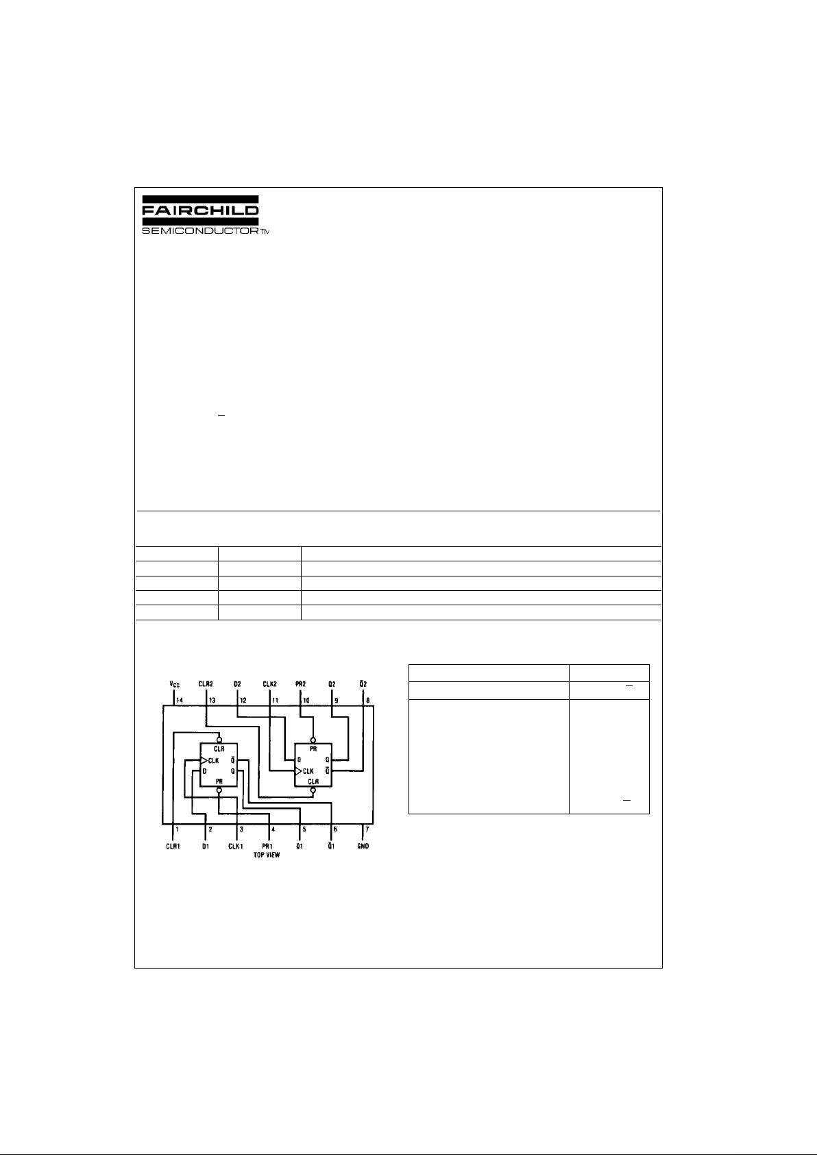
This flip-flop has independent data, preset, clear, and clock
inputs and Q and Q
outputs. The logic level present at t he
data input is transferred to the outpu t during the positivegoing transition of the clock pulse. Preset and clear are
independent of the clock and accomp lished by a low level
at the appropriate input.
The 74HCT logic family is functionally and pin-out compatible with the standard 7 4LS logic family. All inputs are pr o-
tected from damage due to static discharge by internal
diode clamps to V
CC
and ground.
MM74HCT devices are intended to interface between TTL
and NMOS components and standard CMOS devices.
These parts are also plug-in replacements for LS-TTL
devices and can be used to redu ce power consumption in
existing designs.
Features
■ Typical propagation delay: 20 ns
■ Low quiescent current: 40 µA maximum (74HCT Series )
■ Low input current: 1 µA maximum
■ Fanout of 10 LS-TTL loads
■ Meta-stable hardened
Ordering Code:
Devices also available in Tape and Reel. Specify by appending the suffix letter “X” to the ordering code.
Connection Diagram
Pin Assignments for DIP, SOIC, SOP and TSSOP
Truth Table
Q0 = the level of Q before the indicated input conditions were established.
Note 1: This configuration is nonst able; that is, it will not pers ist when pre-
set and clear inputs ret urn to their inactive (HIGH) level.
Order Number Package Number Package Description
MM74HCT74M M14A 14-Lead Small Outline Integrated Circuit (SOIC), JEDEC MS-120, 0.150” Narrow
MM74HCT74SJ M14D 14-Lead Small Outline Package (SOP), EIAJ TYPE II, 5.3mm Wide
M74HCT74MTC MTC14 14-Lead Thin Shrink Small Outline Package (TSSOP), JEDEC MO-153, 4.4mm Wide
MM74HCT74N N14A 14-Lead Plastic Dual-In-Line Package (PDIP), JEDEC MS-001, 0.300” Wide
Inputs Outputs
PR CLR CLK D Q Q
LHXXHL
HLXXLH
LLXXH
(Note 1)H(Note 1)
HH↑ HHL
HH↑ LLH
HHLXQ0Q
0
www.fairchildsemi.com 2
MM74HCT74
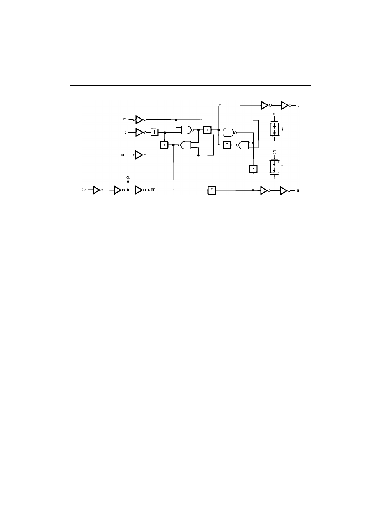
Logic Diagram
3 www.fairchildsemi.com
MM74HCT74
Absolute Maximum Ratings(Note 2)
(Note 3)
Recommended Operating
Conditions
Note 2: Absolute Maximum Rati ngs are tho se values b eyond which d am-
age to the device may occur.
Note 3: Unless otherwise specified all voltages are referenced to ground.
Note 4: Power Dissipation temperature de rating — p lastic “N” p ackage: −
12 mW/°C from 65°C to 85°C.
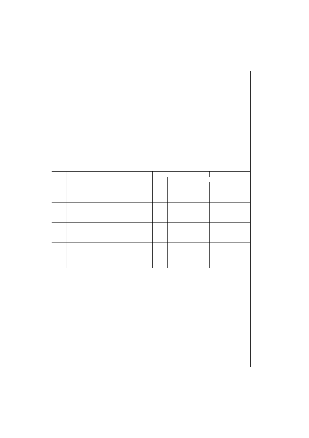
DC Electrical Characteristics
V
CC
= 5V ±10% (unless otherwise specified)
Note 5: This is measured per pin. All other inputs are held at VCC Ground.
Supply Voltage (VCC) −0.5 to +7.0V
DC Input Voltage (V
IN
) −1.5 to V
CC
+1.5V
DC Output Voltage (V
OUT
) −0.5 to V
CC
+0.5V
Clamp Diode Current (I
IK
, IOK) ±20 mA
DC Output Current, per pin (I
OUT
) ±25 mA
DC V
CC
or GND Current, per pin (ICC) ±50 mA
Storage Temperature Range (T
STG
) −65°C to +150°C
Power Dissipation (P
D
)
(Note 4) 600 mW
S.O. Package only 500 mW
Lead Temperature (T
L
)
(Soldering 10 seconds) 260°C
Min Max Units
Supply Voltage (V
CC
)4.55.5V
DC Input or Output Voltage
(V
IN
, V
OUT
)0V
CC
V
Operating Temperature Range (T
A
) −40 +85 °C
Input Rise or Fall Times
(t
r
, tf)500ns
Symbol Parameter Conditions
TA = 25°CTA = −40° to 85°CTA = −55 to 125°C
Units
Typ Guaranteed Limits
V
IH
Minimum HIGH Level 2.0 2.0 2.0 V
Input Voltage
V
IL
Maximum LOW Level 0.8 0.8 0.8 V
Input Voltage
V
OH
Minimum HIGH Level V
IN
= VIH or V
IL
Output Voltage |I
OUT
| = 20 µAV
CCVCC
− 0.1 VCC− 0.1 VCC− 0.1 V
|I
OUT
| = 4.0 mA, V
CC
= 4.5V 4.2 3.98 3.84 3.7 V
|I
OUT
| = 4.8 mA, V
CC
= 5.5V 5.2 4.98 4.84 4.7 V
V
OL
Maximum LOW Level V
IN
= VIH or V
IL
Voltage |I
OUT
| = 20 µA 0 0.1 0.1 0.1 V
|I
OUT
| = 4.0 mA, V
CC
= 4.5V 0.2 0.26 0.33 0.4 V
|I
OUT
| = 4.8 mA, V
CC
= 5.5V 0.2 0.26 0.33 0.4 V
I
IN
Maximum Input V
IN
= VCC or GND, ±0.0.5 ±0.5 ±1.0 µA
Current VIH or V
IL
I
CC
Maximum Quiescent V
IN
= VCC or GND
Supply Current I
OUT
= 0 µA 2.0 20 80 µA
V
IN
= 2.4V or 0.5V (Note 5) 0.3 0.4 0.5 mA
 Loading...