

Fairchild Semiconductor MM74HC594N, MM74HC594MX, MM74HC594M Datasheet
January 1992
Revised May 1999
MM74HC594 8-Bit Shift Register with Output Registers
© 1999 Fairchild Semiconductor Corporation DS010915.prf www.fairchildsemi.com
MM74HC594
8-Bit Shift Register with Output Registers
General Description
This high speed shift register utilizes advanced silicon-gate
CMOS technology. This device possesses the high noise
immunity and low power c onsumption of standard CMOS
integrated circuits, as well as the ability to drive 15 LS-TT L
loads.
This device contains an 8-bit serial-in, parallel-out shift register that feeds an 8-bit D-type storage register. Separate
clocks and direct overriding clears are provided for both the
shift register and the storage register. The shift register has
a direct-overriding clear, serial input, and serial output
(standard) pins for casca ding. Both the shift register and
storage register use posit ive-edge tr iggered clocks. I f both
clocks are connected toget her, the shift register state will
always be one clock pulse ahead of the storage register.
The 74HC logic family is speed, function, an d p in-o ut co mpatible with the sta ndard 74LS logic fami ly. All inputs are
protected from damage due to static discharge by inte rnal
diode clamps to V
CC
and ground.
Features
■ Low quiescent current: 80 µA maximum
■ Low input current: 1 µA maximum
■ 8-bit serial-in, parallel-out shift register with storage
■ Wide operating voltage range: 2V to 6V
■ Cascadable
■ Shift register has direct clear
■ Guaranteed shift frequency: DC to30 MHz
Ordering Code:
Devices also availab le in Tape and Reel. Specify by appending th e s uffix let t er “X” to the ordering cod e.
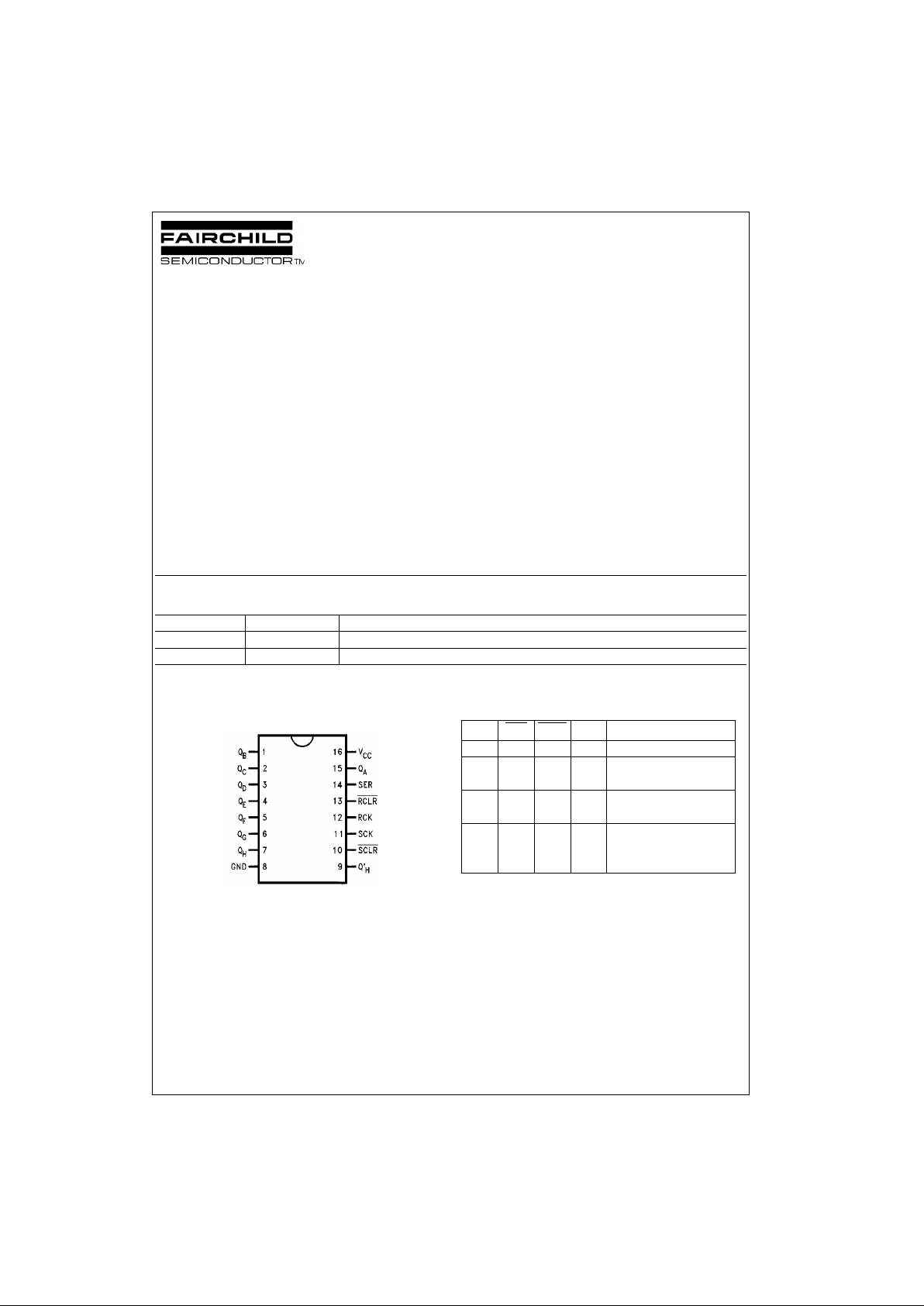
Connection Diagram Truth Table
Order Number Package Number Package Description
MM74HC594M M16A 16-Lead Small Outline Integrated Circuit (SOIC), JEDEC MS-012, 0.150 Narrow
MM74HC594N N16E 16-Lead Plastic Dual-In-Line Package (PDIP), JEDEC MS-001, 0.300 Wide
RCK SCK SCLR RCLR Function
X X X L Storage Register cleared
XXLX
Shift Register cleared
Q’
H
= 0
X ↑ HH
Shift Register clocked
Q
N
= Q
n−1
, Q0 = SER
↑ XHH
Contents of Shift
Register transferred
to output latches
www.fairchildsemi.com 2
MM74HC594
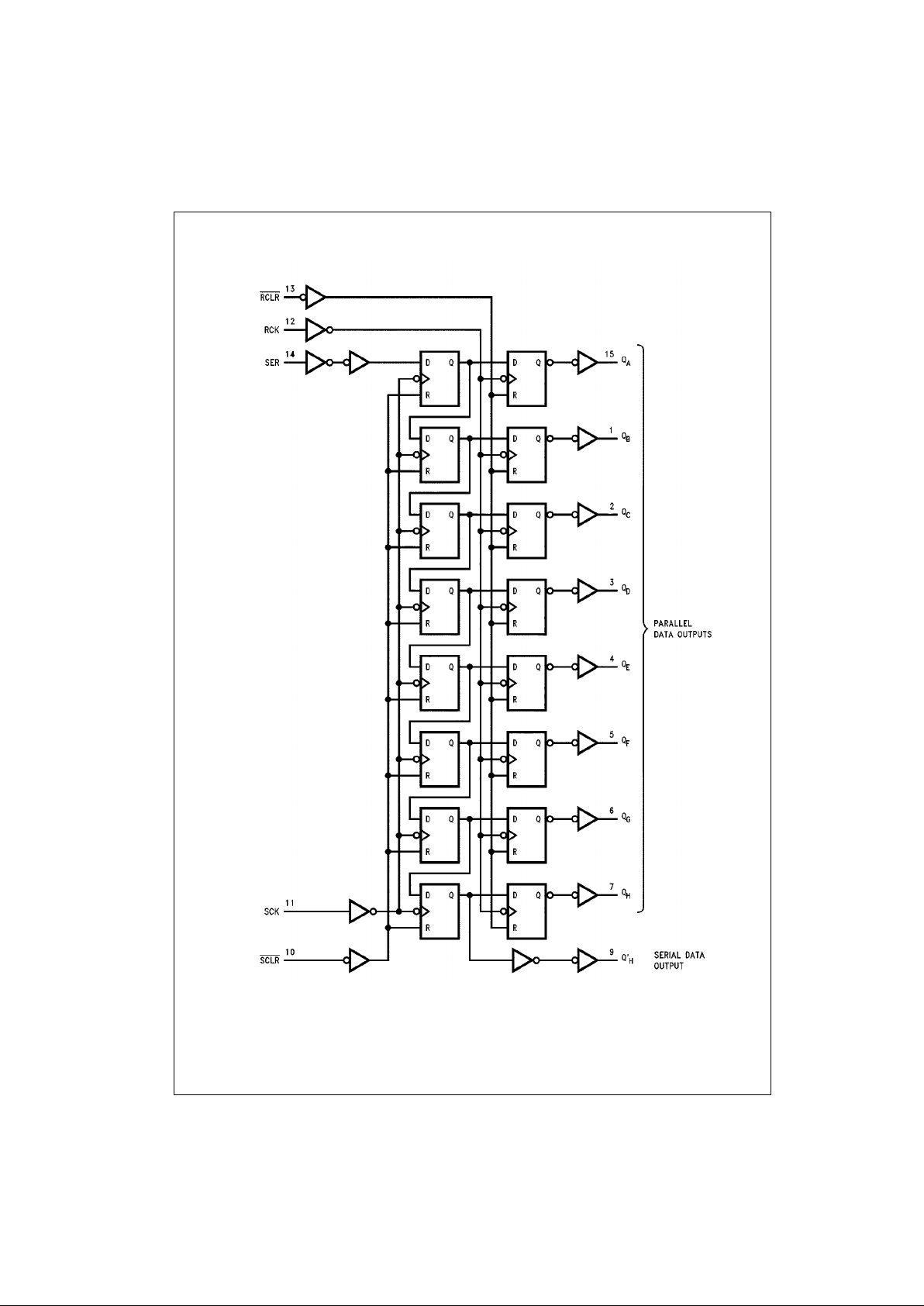
Logic Diagram
3 www.fairchildsemi.com
MM74HC594
Absolute Maximum Ratings(Note 1)
(Note 2)
Recommended Operation
Conditions
Note 1: Absolute Maximum Ra tings are those valu es beyond w hich dam-
age to the device may occur.
Note 2: Unless otherwise specified all voltages are referenced to ground.
Note 3: Power Dissipation temperature derating—plastic “N” pac k age: −12
mW/°C from 65°C to 85°C.
DC Electrical Characteristics (Note 4)
Note 4: For a powe r supply o f 5V ±10% the worst case output voltages (VOH, and VOL) occur for HC at 4.5V. Thus the 4. 5V valu es shou ld be u sed when
designing with this supply. Worst case V
IH
and VIL occur at VCC = 5.5V and 4.5 V respectively. (The VIH value at 5.5V is 3.85V.) The worst case leakage cur-
rent (I
IN
, ICC, and IOZ) occur for CMOS at the higher voltage and so th e 6. 0V values should be used.
Supply Voltage (VCC) −0.5 to +7.0V
DC Input Voltage (V
IN
) −1.5 to VCC +1.5V
DC Output Voltage (V
OUT
) −0.5 to VCC +0.5V
Clamp Diode Current (I
IK
, IOK) ±20 mA
DC Output Current, per pin (I
OUT
) ±35 mA
DC V
CC
or GNDCurrent,per pin(ICC) ±70 mA
Storage Temperature Range (T
STG
) −65°C to +150°C
Power Dissipation (P
D
)
(Note 3) 600 mW
S.O. Package only 500 mW
Lead Temperature (T
L
)
(Soldering 10 seconds) 260°C
Min Max Units
Supply Voltage (V
CC
)26V
DC Input or Output Voltage 0 V
CC
V
(V
IN
, V
OUT
)
Operating Temperature Range (T
A
) −40 +85 °C
Input Rise or Fall Times
(t
r
, tf)VCC = 2.0V 1000 ns
V
CC
= 4.5V 500 ns
V
CC
= 6.0V 400 ns
Symbol Parameter Conditions
V
CC
TA = 25°CT
A
= −40 to 85°C
Units
Typ Guaranteed Limits
V
IH
Minimum HIGH Level 2.0V 1.5 1.5
VInput Voltage 4.5V 3.15 3.15
6.0V 4.2 4.2
V
IL
Maximum LOW Level 2.0V 0.5 0.5
VInput Voltage 4.5V 1.35 1.35
6.0V 1.8 1.8
V
OH
Minimum HIGH Level VIN = VIH or V
IL
V
Output Voltage |I
OUT
| ≤ 20 µA 2.0V 2.0 1.9 1.9
4.5V 4.5 4.4 4.4
6.0V 6.0 5.9 5.9
Q’
H
VIN = VIH or V
IL
V|I
OUT
| ≤ 4.0 mA 4.5V 4.7 3.98 3.84
|I
OUT
| ≤ 5.2 mA 6.0V 5.2 5.48 5.34
QA thru Q
H
VIN = VIH or V
IL
V|I
OUT
| ≤ 6.0 mA 4.5V 4.2 3.98 3.84
|I
OUT
| ≤ 7.8 mA 6.0V 5.7 5.48 5.34
V
OL
Maximum LOW Level VIN = VIH or V
IL
V
Output Voltage |I
OUT
| ≤ 20 µA2.0V00.10.1
4.5V 0 0.1 0.1
6.0V 0 0.1 0.1
Q’
H
VIN = VIH or V
IL
V|I
OUT
| ≤ 4.0 mA 4.5V 0.2 0.26 0.33
|I
OUT
| ≤ 5.2 mA 6.0V 0.2 0.26 0.33
QA thru Q
H
VIN = VIH or V
IL
V|I
OUT
| ≤ 6.0 mA 4.5V 0.2 0.26 0.33
|I
OUT
| ≤ 7.8 mA 6.0V 0.2 0.26 0.33
I
IN
Maximum Input VIN = VCC or GND 6.0V ±0.1 ±1.0 µA
Current
I
CC
Maximum Quiescent VIN = VCC or GND 6.0V 8.0 80 µA
Supply Current I
OUT
= 0 µA
 Loading...