

Fairchild Semiconductor MM74HC4538SJ, MM74HC4538MX, MM74HC4538SJX, MM74HC4538N, MM74HC4538M Datasheet
© 2000 Fairchild Semiconductor Corporation DS005217 www.fairchildsemi.com
February 1984
Revised August 2000
MM74HC4538 Dual Retriggerable Monostable Multivibrator
MM74HC4538
Dual Retriggerable Monostable Multivibrator
General Description
The MM74HC4538 high speed monostable multivibrator
(one shots) is implemented in advanced silicon-gate
CMOS technology. They feature speeds comparable to low
power Schottky TTL circuitry whil e retaining the l ow power
and high noise immunity characteristic of CMOS circuits.
Each multivibrator fea tures b oth a n egative , A, a nd a po sitive, B, transition trigg ered input, either of which can be
used as an inhibit input. Also includ ed is a clear input that
when taken low rese ts the one shot . The M M74HC 4538 is
retriggerable. Th at is, it may be triggered repeatedly w hile
their outputs are generating a pulse and the pulse will be
extended.
Pulse width stability over a wide range of temperature and
supply is achieved using linear CMOS techniques. The output pulse equatio n is s imply: PW
= 0.7(R)(C) where PW is
in seconds, R is in ohms, and C is in fa rads. This de vice is
pin compatible with the CD4528, and the CD4538 one
shots. All inputs are prote cted from damage due to stat ic
discharge by diodes to V
CC
and ground.
Features
■ Schmitt trigger on A and B inputs
■ Wide power supply range: 2–6V
■ Typical trigger propagation delay: 32 ns
■ Fanout of 10 LS-TTL loads
■ Low input current: 1
µA max
Ordering Code:
Devices also availab le in Tape and Reel. Specify by appending th e s uffix let t er “X” to the ordering code.
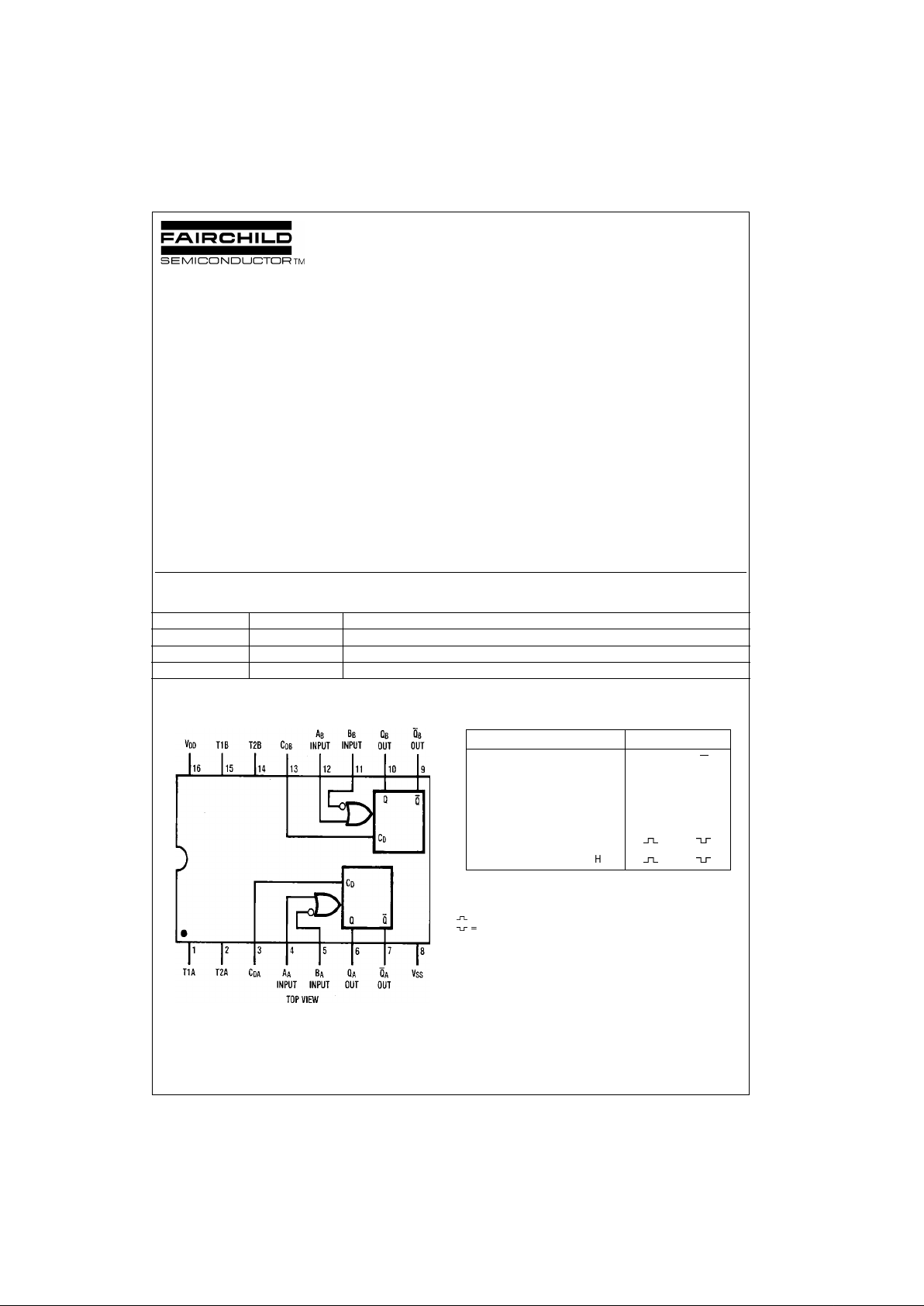
Connection Diagram Truth Table
H = HIGH Level
L = LOW Level
↑ = Transition from LOW-to-HIGH
↓ = Transition from HIGH -t o-LOW
= One HIGH Level Pulse
= One LOW Level Pu ls e
X = Irrelevant
Order Number Package Number Package Description
MM74HC4538M M16A 16-Lead Small Outline Integrated Circuit (SOIC), JEDEC MS-012, 0.150 Narrow
MM74HC4538SJ M16D 16-Lead Small Outline Package (SOP), EIAJ TYPE II, 5.3mm Wide
MM74HC4538N N16E 16-Lead Plastic D ual-In-Line Package (PDIP), JEDEC MS-001, 0.300 Wide
Inputs Outputs
Clear A B Q Q
LXXLH
XHXLH
XXLLH
HL
↓
H ↑ H
www.fairchildsemi.com 2
MM74HC4538
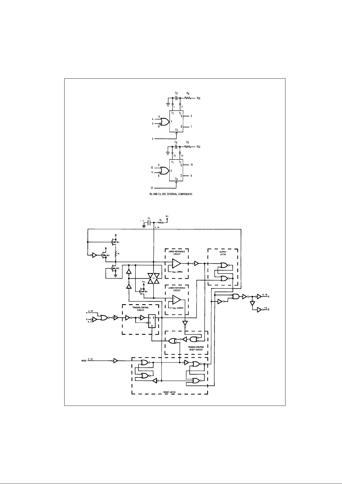
Block Diagrams
Note: Pin 1 and Pin 15 must be hard-wired to GND.
Logic Diagram
3 www.fairchildsemi.com
MM74HC4538
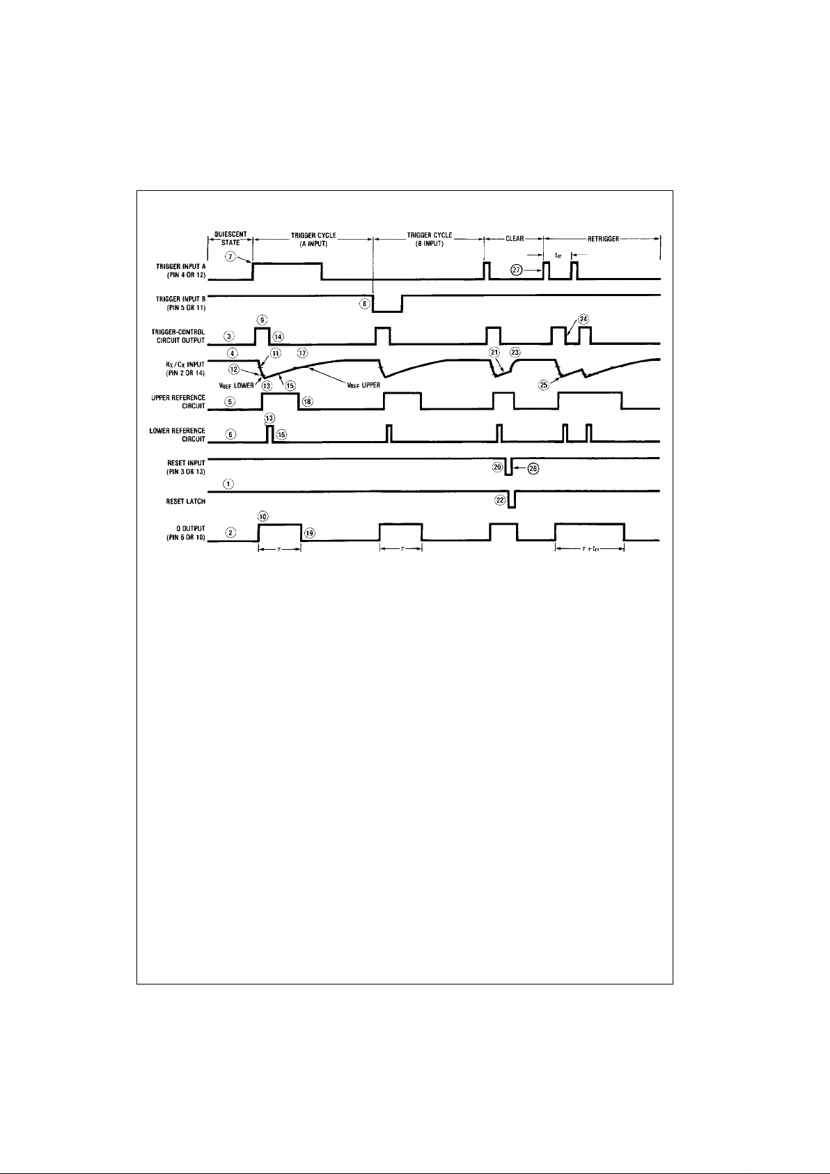
Timing Diagram
Circuit Operation
The MM74HC4538 op erates as follow s (refer to lo gic diagram). In the quiescent state, th e external timing capacitor,
C
X
, is charged to VCC. When a trigger occurs, the Q output
goes HIGH and C
X
discharges quickly to the lowe r refer-
ence voltage (V
REF
Lower = 1/3 VCC). CX then charges,
through R
X
, back up to the upper refere nce voltage (V
REF
Upper = 2/3 VCC), at which point the one-shot has timed out
and the Q output goes LOW.
The following, more de tailed description of the ci r cuit o pe r-
ation refers to both the logic diagram and the timing diagram.
QUIESCENT STATE
In the quiescent state, before an inp ut trigger appe ars, the
output latch is HIGH and the reset latch is HIGH (#1 in logic
diagram).
Thus the Q output (pin 6 or 10) of the mono stable multivi brator is LOW (#2, timing diagram).
The output of the trigge r-control circuit is LOW (#3), and
transistors M1, M2, and M3 are turned off. The external
timing capacitor, C
X
, is charged to VCC (#4), and the upper
reference circuit has a LO W output (#5). Transistor M4 i s
turned ON and transmission gate T1 is turned OFF. Thus
the lower reference circuit has V
CC
at the noninverting
input and a resulting LOW output (#6).
In addition, the output of the trigger-con trol reset circuit is
LOW.
TRIGGER OPERATION
The MM74HC4538 is tr iggere d by e ithe r a r ising -edge signal at input A (#7) or a falling-edge signal at input B (#8),
with the unused tr igger input and the Reset input held a t
the voltage levels sho wn in the Truth Table. Either trigger
signal will cause the output of the trigger-control circuit to
go HIGH (#9).
The trigger-control circ uit going HIGH simultaneously initiates three events. Fir st, the output l atch goes LOW, thus
taking the Q output of the HC4538 to a H IGH State (#10) .
Second, transistor M3 is tur ned on , whi ch allows the external timing capacitor, C
X
, to rapidly discharge toward
ground (#11). (Note that the voltag e across C
X
appears at
the input of the upper refer ence circuit comp arator.) Third,
transistor M4 is turned off and transmission gate T1 is
turned ON, thus allowing the voltage across C
X
to also
appear at the input of the lowe r reference circuit comparator.
When C
X
discharges to the referen ce voltage of the low er
reference circuit (#12), the outputs of both reference circuits will be HIGH (#13). The trigger-control reset circuit
goes HIGH, resetting the trigger-control circuit flip-flop to a
LOW State (#14). This turns transistor M3 OFF again,
allowing C
X
to begin to charge back up toward VCC, with a
time constant t
= R
XCX
(#15). In addition, tran sistor M4 is
turned ON and transmission gate T1 is turned OFF. Thus a
high voltage level is applied to the input of the lower reference circuit comparator, causing its output to go LOW
(#16). The monos table multivi brator may b e retriggere d at
any time after the trigger-control circuit goes LOW.
When C
X
charges up to the reference vo ltag e of the up per
reference circuit (#17) , the output of the upper reference
circuit goes LOW (#1 8). This causes the output latch to
 Loading...