


Fairchild Semiconductor MM74C911N Datasheet
October 1987
Revised January 1999
MM74C911 4-Digit Expandable Segment Display Controller
© 1999 Fairchild Semiconductor Corporation DS005915.prf www.fairchildsemi.com
MM74C911
4-Digit Expandable Segment Display Controller
General Description
The MM74C911 display controller is an interface element
with memory th at drives a 4-digit, 8-seg ment LED d isplay.
The MM74C911 allows individual control of any segment in
the 4-digit display. The number of segments per digit can
be expanded without any exter nal c omponent s. For example, two MM74C911’s can be cascade d to drive a 16-se gment alpha-numeric display.
The display controllers receive data infor mation through 8
data lines a, b…DP, and digit information through 2
address inputs K1 and K2. The input data is written into the
register selected by the address information when CHIP
ENABLE, CE, a nd WRITE ENABLE, WE, are LOW and is
latched when either CE
or WE return HIGH. Data hold time
is not required.
A self-contained internal oscillator sequentially presents
the stored data to hi g h d r ive (100 m A typ.) 3-STATE output
drivers which directly drive the LED display. The drivers are
active when the control pin labeled SEGMENT OUTPUT
ENABLE, SOE, is LOW and go into 3-STATE when SOE is
HIGH. This feature allows for duty cycle brightness control,
or for disabling the output drive for power conservation.
The digit outputs dire ctl y d r ive the ba se of the d ig it t ransistor when the control pi n labeled DIGIT INPUT OUTPUT
,
DIO
, is LOW. When DIO is HIGH, the digit lines turn into
inputs and the internal scanning multiplexer is disabled.
When any digit line is forced H IGH by an external device,
usually another MM74 C911, the data information for that
digit is presented to the output. In this manner, 16-segment
alpha-numeric displ ays, 24- or 32-segment di splays, or an
array of discrete LED's can be controlled by the simple cascading of expandable segment display controllers. All
inputs except digit inpu ts are TTL compatible and do not
clamp input voltages above V
CC
.
Features
■ Direct segment drive (100 mA typ.) 3-STATE
■ 4 registers addressed like RAM
■ Internal oscillator and scanning circuit
■ Direct base drive to digit transistor
■ Segment expandability without external components
■ TTL compatible inputs
■ Power saver mode—5 µW (typ.)
Ordering Code:
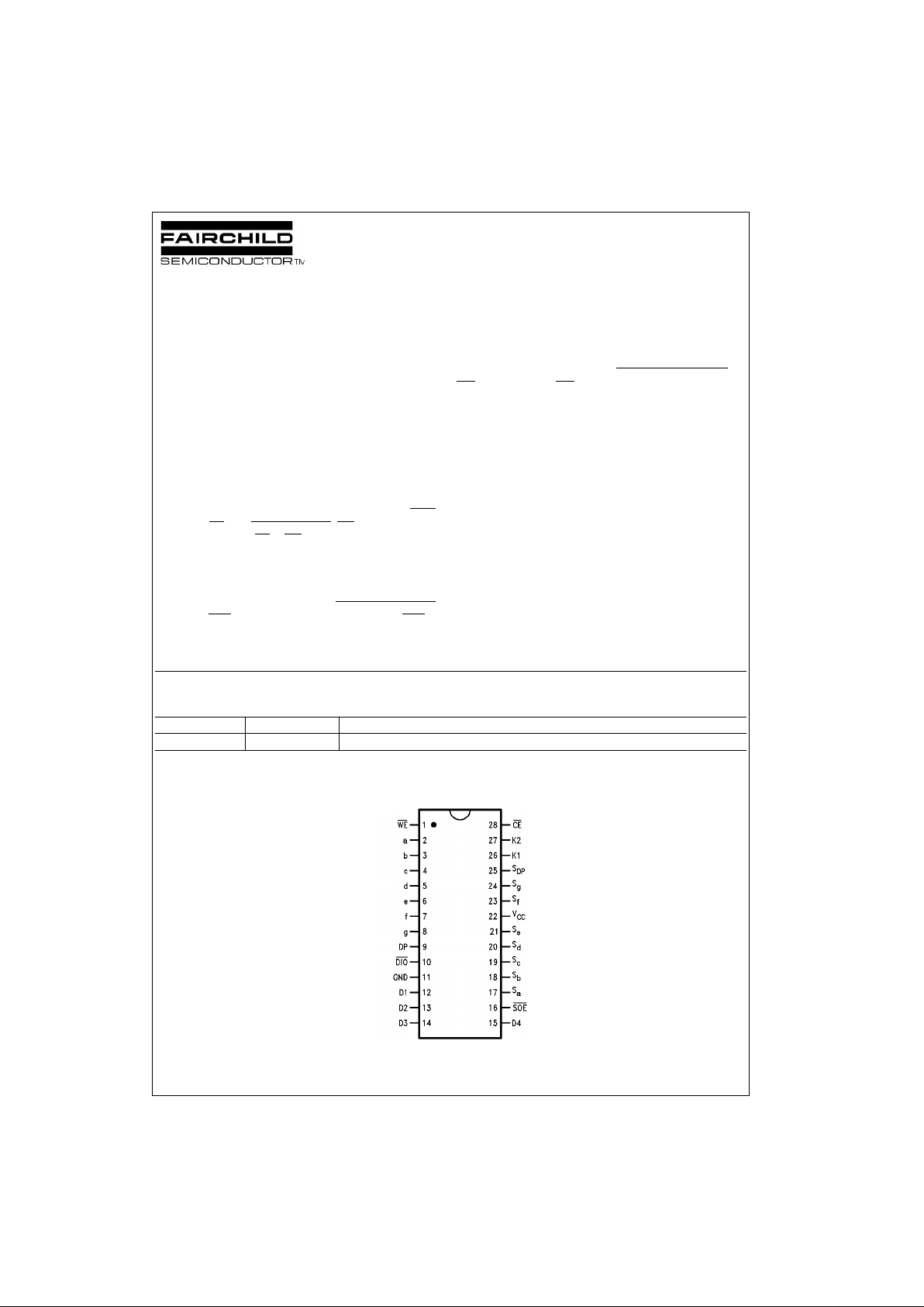
Connection Diagram
Pin Assignments for DIP
Top View
Order Number Package Number Package Description
MM74C991N N28B 28-Lead Plastic Dual-In-Line Package (PDIP), JEDEC MS−010, 0.600” Wide
www.fairchildsemi.com 2
MM74C911
Truth Tables
Input Control Output Control
R = Refresh (digit line s se quentially pulsed)
X = Don’t Care
Functional Description
The MM74C911 display controller is manufactured on standard metal gate CMOS techno logy. A single 5V 74 series
TTL supply can be used for power and should be bypassed
at the V
CC
pin to suppress current transients.
The digit outputs directly drive the base of a grounded
emitter digit transistor without the need of a Darlington configuration. If an MM 74C911 i s drivi ng a digit transistor an d
also supplying digit information to a cascaded MM74C911,
base resistors are nee de d in th e di g it transistors to provide
an adequate high level to the digit inputs of the cascaded
MM74C911.
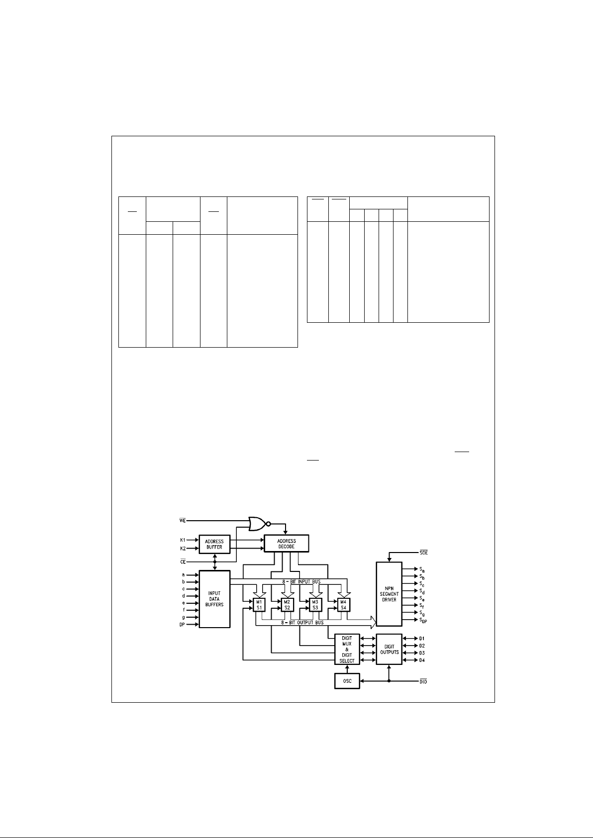
As seen in the Block Diagram, these display controllers
contain four 8-bit registe rs; any on e may be randoml y wr it-
ten into. In normal op eratio n, the i nte rnal multiplexer scans
the registers and refresh es th e di sp lay. In cascaded operation, 1 MM74C911 serves as a master refresh device and
cascaded MM74C911’s are slaved to it throu gh digit lines
operating as inputs.
The MM74C911 appea rs to a microprocessor a s memory
and to the user as a self-scan display. Since every segment is under microprocessor control, great versatility is
obtained.
Low power standby operation occurs w ith both SOE
and
DIO
inputs HIGH. This condition forces the MM74C911 to a
quiescent state typically drawing less than 1 µA of supply
current with a standby supply voltage as low as 3V.
Logic Diagram
Digit
CE
Address WE Operation
K2 K1
0 0 0 0 Write Digit 1
0 0 0 1 Latch Digit 1
0 0 1 0 Write Digit 2
0 0 1 1 Latch Digit 2
0 1 0 0 Write Digit 3
0 1 0 1 Latch Digit 3
0 1 1 0 Write Digit 4
0 1 1 1 Latch Digit 4
1 X X X Disable Writing
DIO SOE Digit Lines Operation
D4 D3 D2 D1
0 0 RRRRRefresh Display
0 1 RRRRDisable Segment Outputs
1 0 0000Digits Are Now Inputs
1 0 0001Display Digit 1
1 0 0010Display Digit 2
1 0 0100Display Digit 3
1 0 1000Display Digit 4
1 1 0000Power Saver Mode
3 www.fairchildsemi.com
MM74C911
Absolute Maximum Ratings(Note 1)
(Note 2)
Note 1: “Absolute Maximum Rat ings” are tho se values beyond which the
safety of the device cannot be guarant eed. Exce pt for “Operating Range”,
they are not meant to imply that the device should be operated at these limits. The table of “Electr ical Characteristic s” provides condition s for actual
device operation.
Note 2: All voltage reference to ground.
DC Electrical Characteristics
Min/Max limits apply at −40°C ≤ TJ ≤ +85°C, unless otherwise noted
Note 3: θJA measured in free-air with device soldered into printed circuit board.
Voltage at Any Pin
except Inputs −0.3V to V
CC
+ 0.3V
Voltage at Any Input
except Digits −0.3V to +15V
Operating Temperature
Range, (T
A
) −40°C to +85°C
Storage Temperature Range −65°C to +150°C
Power Dissipation (P
D
) Refer to P
D(MAX)
vs TA Graph
Operating V
CC
Range 3V to 6V
Absolute Maximum V
CC
6.5V
Lead Temperature
(Soldering , 10 seconds) 260°C
Symbol Parameter Conditions Min Typ Max Units
V
IN(1)
Logical “1” Input Voltage VCC = 5V 3.0 V
V
IN(0)
Logical “0” Input Voltage 1.5 V
I
IN(1)
Logical “1” Input Current VCC = 5V, VIN = 15V 0.005 1.0 µA
I
IN(0)
Logical “0” Input Current VCC = 5V, VIN = 0V −1.0 −0.005 µA
I
CC
Supply Current (Normal) VCC = 5V, Outputs Open 0.50 2.5 mA
I
CC
Supply Current (Power Saver)
VCC = 5V, SOE, DIO = “1”,
1 600 µA
D1, D2, D3, D4 = “0”
I
OUT
3-STATE Output Current VO = 5V 0.03 10 µA
VO = 0V −10 −0.03
CMOS/LPTTL INTERFACE
V
IN(1)
Logical “1” Input Voltage VCC = 4.75V VCC − 2V
V
IN(0)
Logical “0” Input Voltage VCC = 4.75V 0.8 V
OUTPUT DRIVE
I
SH
HIGH Level Segment Current VCC = 5V, VO = 3.4V
TJ = 25°C −60 −100 mA
TJ = 100°C −40 −60 mA
I
DH
HIGH Level Digit Current VCC = 5V, VO = 3V
TJ = 25°C −10 −20 mA
TJ = 100°C −7 −10 mA
VCC = 5V, VO = 1V
TJ = 25°C −15 −40 mA
TJ = 100°C −10 −15 mA
V
OUT(1)
Logical “1” Output Voltage, VCC = 5V, IO = −360 µA4.6 V
Any Digit
V
OUT(0)
Logical “0” Output Voltage, VCC = 5V, IO = 360 µA0.4V
Any Output
θ
JA
Thermal Resistance (Note 3) 100 °C/W