

Fairchild Semiconductor MM74C08N Datasheet
MM74C08
Quad 2-Input AND Gate
MM74C08 Quad 2-Input AND Gate
October 1987
Revised January 1999
General Description
The MM74C08 employs complementary MOS (CMOS)
transistors to achieve wide power supply operatin g range,
low power consumption and high noise margin, these
gates provide basic functions used in the implementation of
digital integrated circuit systems. The N- and P-channel
enhancement mode transisto rs provide a symmetrical circuit with output swing essentially equal to the supply voltage. No DC power other than that caused by leakage
current is consumed during static condition. Al l inputs are
protected from da mage due to static discharge by diode
clamps to V
and GND.
CC
Features
■ Wide supply voltage range: 3.0V to 15V
■ Guaranteed noise margin: 1.0V
■ High noise immunity: 0.45 V
■ Low power TTL compatibility:
Fan out of 2 driving 74L
■ Low power consumption: 10 nW/package (typ.)
CC
(typ.)
Ordering Code:
Order Number Package Number Package Description
MM74C08M M14A 14-Lead Small Outline Integrated Circuit (SOIC), JEDEC MS-120, 0.150” Narrow
MM74CD8N N14A 14-Lead Plastic Dual-in-Line Package (PDIP), JEDEC MS-001, 0.300” Wide
Devices also available in Tape and Reel. Specify by appending suffix letter “X” to th e ordering code.
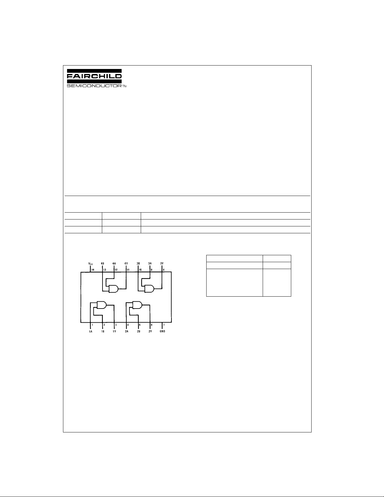
Connection Diagram
Pin Assignments for DIP and SOIC
Truth Table
ABY
LLL
LHL
HLL
HHH
H = HIGH Level
L = LOW Level
Inputs Outputs
Top View
© 1999 Fairchild Semiconductor Corporation DS005878.prf www.fairchildsemi.com
Absolute Maximum Ratings(Note 1)
Voltage at Any Pin −0.3V to VCC + 0.3V
Operating Temperature Range −40°C to +85°C
MM74C08
Storage Temperature Range −65°C to +150°C
Power Dissipa tion (P
Dual-In-Line 700 mW
)
D
Absolute Maximum V
CC
Lead Temperature
(Soldering, 10 seconds) 260°C
Note 1: “Absolute Maxi mum Ratings” are those valu es beyond which the
safety of the device cannot be guaranteed. E x ce pt for “O perating Temperature Range” they are not mean t to imply that the devices sho uld be operated at these limits. The Electrical Ch arac t eristics table provides co nditions
for actual device operation.
Small Outline 500 mW
Operating V
Range 3.0V to 15V
CC
DC Electrical Characteristics
Min/Max limits apply across the guaranteed temperature range, unless otherwise noted
Symbol Parameter Conditions Min Typ Max Units
CMOS TO CMOS
V
IN(1)
V
IN(0)
V
OUT(1)
V
OUT(0)
I
IN(1)
I
IN(0)
I
CC
CMOS/LPTTL INTERFA CE
V
IN(1)
V
IN(0)
V
OUT(1)
V
OUT(0)
OUTPUT DRIVE (see Family Characteristics Data Sheet) TA = 25°C (short circuit current)
I
SOURCE
I
SOURCE
I
SINK
I
SINK
Logical “1” Input Voltage VCC = 5.0V 3.5 V
VCC = 10V 8.0 V
Logical “0” Input Voltage VCC = 5.0V 1.5 V
VCC = 10V 2.0 V
Logical “1” Output Voltage VCC = 5.0V, IO = −10 µA4.5 V
VCC = 10V, IO = −10 µA9.0 V
Logical “0” Output Voltage VCC = 5.0V, IO = 10 µA0.5V
VCC = 10V, IO = 10 µA1.0V
Logical “1” Input Current VCC = 15V, VIN = 15V 0.005 1.0 µA
Logical “0” Input Current VCC = 15V, VIN = 0V −1.0 −0.005 µA
Supply Current VCC = 15V 0.01 15 µA
Logical “1” Input Voltage 74C, VCC = 4.75V VCC − 1.5 V
Logical “0” Input Voltage 74C, VCC = 4.75V 0.8 V
Logical “1” Output Voltage 74C, VCC = 4.75V, IO = −360 µA2.4 V
Logical “0” Output Voltage 74C, VCC = 4.75V, IO = 360 µA0.4V
Output Source Current VCC = 5.0V, V
= 0V −1.75 −3.3 mA
OUT
(P-Channel)
Output Source Current VCC = 10V, V
= 0V −8.0 15 mA
OUT
(P-Channel)
Output Sink Current VCC = 5.0V, V
OUT
= V
CC
1.75 3.6 mA
(N-Channel)
Output Sink Current VCC = 10V, V
OUT
= V
CC
8.0 16 mA
(N-Channel)
18V
www.fairchildsemi.com 2
 Loading...