

Fairchild Semiconductor KSH200 Datasheet
KSH200
D-PAK for Surface Mount Applications
• High DC Current Gain
• Built-in a Damper Diode at E-C
• Lead Formed for Surface Mount Applications (No Suffix)
• Straight Lead (I-PAK, “ - I “ Suffix)
NPN Epitaxial Silicon Transistor
11
D-PAK I-PAK
1.Base 2.Collector 3.Emitter
KSH200
Absolute Maximum Ratings
TC=25°C unless otherwise noted
Symbol Parameter Value Units
V
CBO
V
CEO
V
EBO
I
B
I
C
I
CP
P
C
T
J
T
STG
Electrical Characteristics
Collector-Base Voltage 40 V
Collector-Emitter Voltage 25 V
Emitter-Base Voltage 8 V
Base Current 1 A
Collector Current (DC) 5 A
Collector Current (Pulse) 10 A
Collector Dissipation (TC = 25°C) 12.5 W
Collector Dissipation (T
= 25°C) 1.4 W
a
Junction Temperature 150 °C
Storage T emperature - 55 ~ 150 °C
TC=25°C unless otherwise noted
Symbol Parameter Test Condition Min. Max. Units
V
(sus) * Collector Emitter Sustaining Voltage IC=100mA, IB=0 25 V
CBO
I
CEO
I
CBO
I
EBO
h
FE
(sat) * Collector-Emitter Saturation Voltage IC=500mA, IB=50mA
V
CE
(sat) * Base-Emitter Saturation Voltage IC=5A, IB=2A 2.5 V
V
BE
(on) * Base-Emitter On Voltage VCE=1V, IC=2A 1.6 V
V
BE
f
T
C
ob
* Pulse Test: PW≤300µs, Duty Cycle≤2%
Collector Cut-off Current VCB=40V, IE=0 100 nA
Collector Cut-off Current V
=8V, IC=0 100 nA
EBO
Emitter Cut-off Current VCE=1V, IC=500mA 70
* DC Current Gain VCE=1V, IC=2A
V
=2V, IC=5A
CE
45
10
180
0.3
=2A, IB=200mA
I
C
=5A, IB=1A
I
C
0.75
1.8
Current Gain Bandwidth Product VCE=10V, IC=100mA 65 MHz
Output Capacitance VCB=10V, IE=0, f=0.1MHz 80 pF
V
V
V
©2002 Fairchild Semiconductor Corporation Rev. A3, October 2002
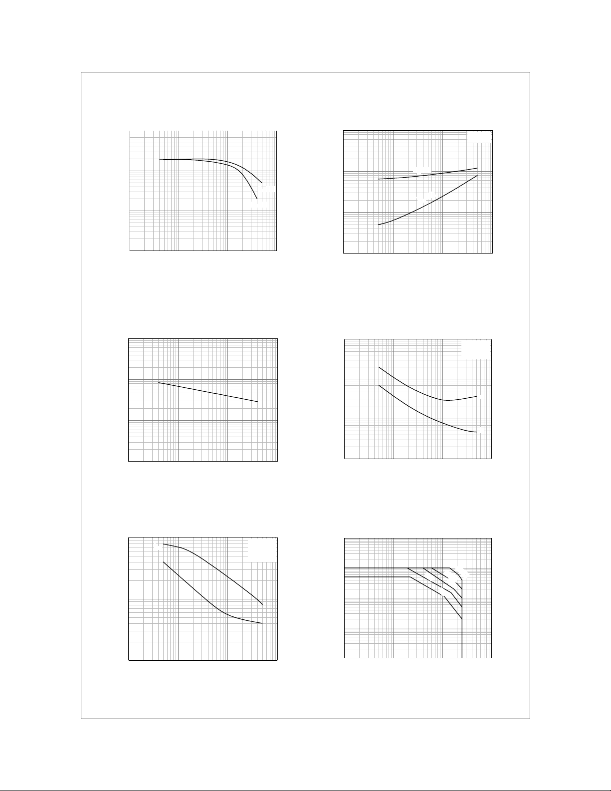
Typical Characteristics
KSH200
1000
100
10
, DC CURRENT GAIN
FE
h
1
0.01 0.1 1 10
IC[A], COLLECTOR CURRENT
Figure 1. DC current Gain Figure 2. Base-Emitter Saturation Voltage
1000
100
10
[pF], CAPACITANCE
ob
C
VCE=2V
VCE=1V
10
1
0.1
(sat) [V], SATURATION VO LTA G E
BE
(sat), V
CE
0.01
V
0.01 0.1 1 10
VBE(sat)
V
CE
(sat)
IC=10I
B
IC[A], COLLECTOR CURRENT
Collector-Emitter Saturation Voltage
10
1
0.1
[ns], TURN ON TIME
D
,t
R
t
VCC=30V
=10I
I
C
B
t
R
t
D
1
0.1 1 10 100
VCB[V], COLLECTOR BASE VOLTAGE
0.01
0.01 0.1 1 10
IC[A], COLLECTOR CURRENT
Figure 3. Collector Output Capacitance Figure 4. Turn On Time
1000
100
[ns], TURN OFF TIME
F
,t
STG
t
10
0.01 0.1 1 10
t
STG
t
F
IC[A], COLLECTOR CURRENT
VCC=30V
=10I
I
C
IB1=-I
B2
100
B
10
1
0.1
[A], COLLECTOR CURRENT
C
I
0.01
0.1 1 10 100
VCE[V], COLLECTOR-EMITTER VOLTAGE
100
500
5ms
µ
s
µ
s
1ms
DC
Figure 5. Turn Off Time Figure 6. Safe Operating Area
©2002 Fairchild Semiconductor Corporation Rev. A3, October 2002
 Loading...