

Fairchild Semiconductor KA7525B Datasheet
©2002 Fairchild Semiconductor Corporation
www.fairchildsemi.com
Rev.1.0.1
Features
• Internal Start-up Timer
• Internal Current Sense Blanking Which Eliminates the
Need for an External R/C filter
• Overvoltage Comparator Eliminates Runaway Output
Voltage
• Zero Current Detector
• One Quadrant Multiplier
• Trimmed 1.5% Internal Bandgap Reference
• Under Voltage Lock Out with 2.1V of Hysteresis
• Totem Pole Output with High State Clamp
• Low Start-up and Operating Current
• 8-Pin DIP or 8-Pin SOP.
Applications
• Electronic Ballast
•SMPS
Description
The KA7525B provides simple and high perform ance activ e
power factor correction. KA7525B is optimized for
electronic ballast and low power, high density power
supplies requiring a minimum board area, reduced
component count and low power dissipation. Addition of
internal current sense blanking (In ternal R,C) eliminates the
need for an external R/C filter. Internal clamping of the error
amplifier and multiplier outputs improves turn on overshoot
characteristics and current limiting. Special circuitry has also
been added to pr event no load runawa y conditions. Outpu t
drive clamps limiting power MOSFET gate drive
independent of supply voltage greatly enhance the products
practical application.
KA7525B
KA7525BKA7525B
KA7525B
Po wer Factor Correction Controller
Po wer Factor Correction ControllerPo wer Factor Correction Controller
Po wer Factor Correction Controller
8-DIP
8-SOP
1
1
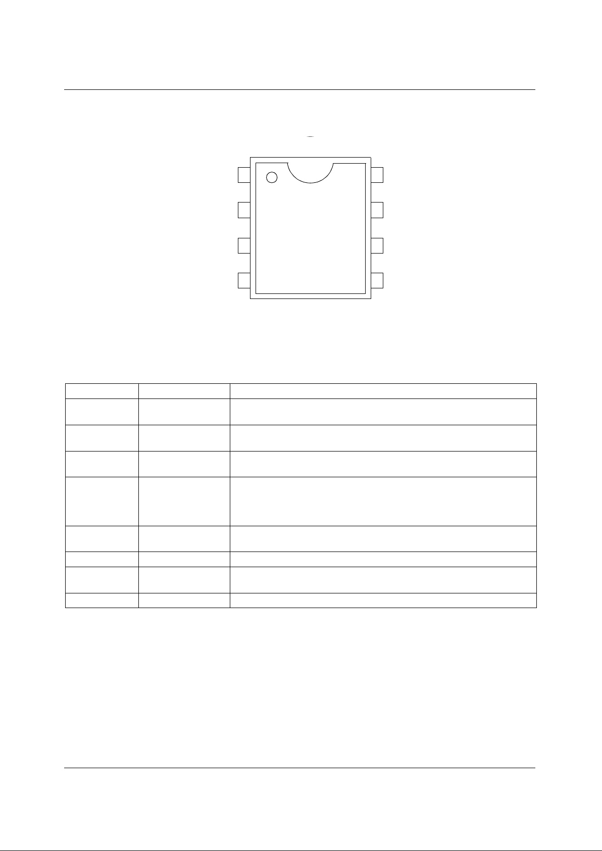
KA7525B
2
Pin Assignments
Pin Definitions
Pin Number Pin Name Pin Function Description
1 INV
Inverting input of the error amplifier. The output of the Boost converter
should be resistively divided to 2.5V and connected to this pin.
2EA_OUT
The output of the error amplifier. A feedback compensation network is
placed between this pin and the INV pin.
3MULT
Input of the multiplier stage. The full-wave rectified AC is divided to less
than 2V and is connected to this pin.
4CS
Input of the PWM comparator. Current is sensed in the Boost stage
MOSFET by a resistor in the source lead. An internal leading edge
blanking circuitry has been included to reject any high frequency noise
present on the current waveform.
5 Idet
The zero current detector senses the inductor current by monitoring
when the Boost inductor auxiliary winding voltage falls below 1.8V.
6 GND The ground potential of all the pins.
7OUT
The output of a high current power driver capable of driving the gate of a
power MOSFET.
8 Vcc The logic and control power supply connection.
1
2
3
45
6
7
8INV
EA OUT
MULT
CS
Vcc
OUT
GND
Idet
(Top View)
KA7525B
3
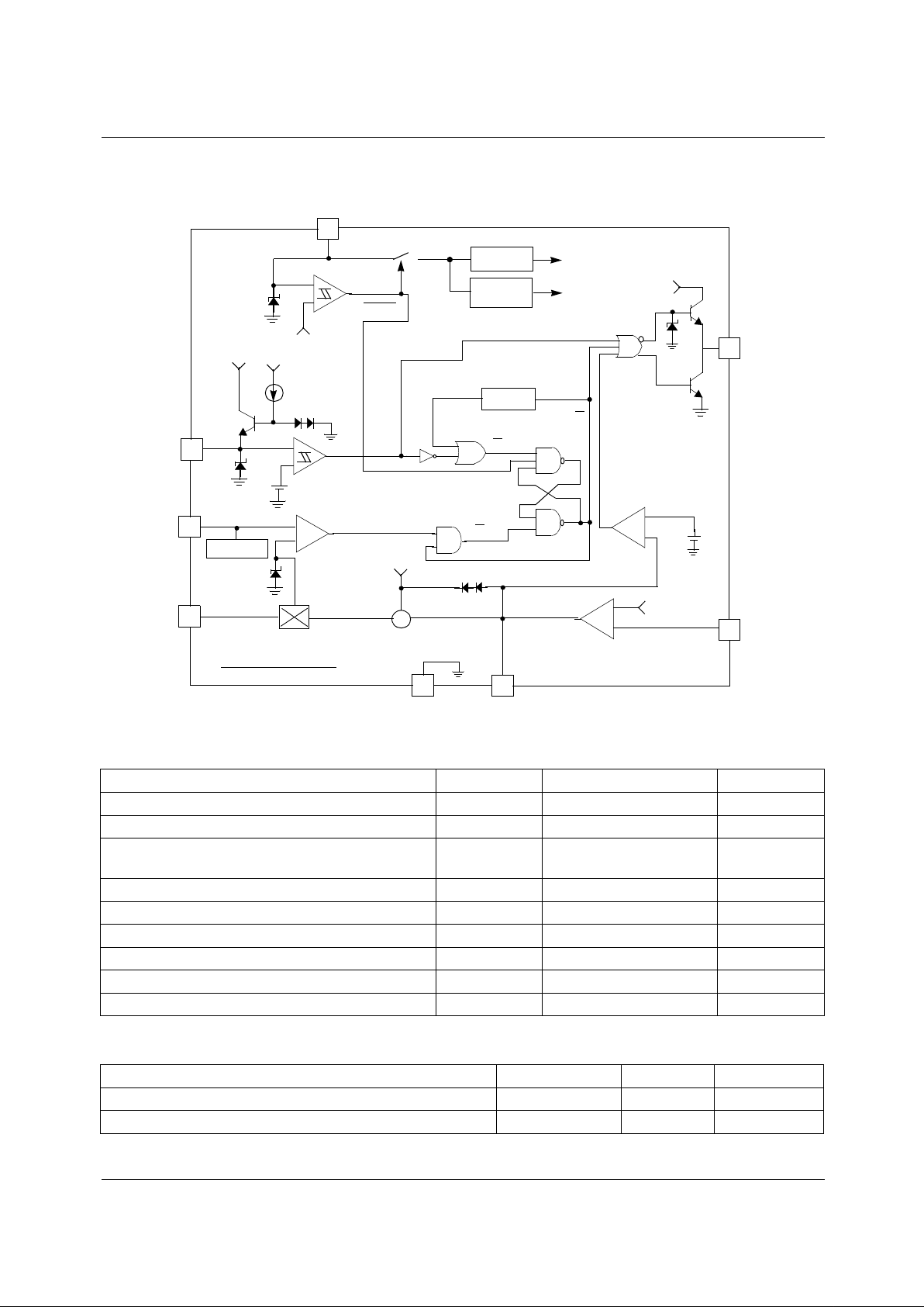
Internal Block Diagram
Absolute Maximum Ratings
Temperature Characteristics (0°°°°C ≤
≤ ≤
≤ Ta ≤
≤ ≤
≤ 125°°°°C )
Parameter Symbol Value Unit
Supply Voltage V
CC
30 V
Peak Drive Output Current Ioh, IoI ±500 mA
Driver Output Clamping Diodes
V
O
> VCC or VO < -0.3V
Iclamp ±10 mA
Detector Clamping Diodes Idet ±10 mA
Error Amp, Multiplier and Comparator Input Voltage Vin -0.3 to 6 V
Operating Temperature Range Topr 0 to 125 °C
Storage Temperature Range Tstg -65 to 150 °C
Power Dissipation Pd 0.8 W
Thermal Resistance (Junction-to-Air) Rθja 100 °C/W
Characteristics Symbol Value Unit
Temperature Stability for Reference Voltage(Vref) ∆Vref (Typ) 20 mV
Temperature Stability for Multiplier Gain(K) ∆K/∆T (Typ) -0.2 %/°C
8
7
5
4
3
1
62
2.5V Ref
Internal
Bias
OUT
INV
EA OUT
GND
MULT
CS
Idet
Vcc
Timer R
R,C Filter
Vref
Vea(-)
Error Amp
Vm2
Vref ~ Vref+1V
Multiplier
0 ~2V
Vm1
Vmo
Drive
Output
Over Voltage
Protection
1.8V
+
-
Current Sense
Comparator
Vref
Zero Current
Detector
240mV
Vcc
1.8V
7.5V
1.24V
10V
36V
2.1V
+
_
+
_
-
+
+
_
+
_
UVLO
Q
R
S
K =
Vm1× (Vm2-Vref)
Pin4 Threshold(Vmo)

KA7525B
4
Electrical Characteristics
Unless otherwise specified, these specifications apply over the operating ambient temperatures for the KA7525B
with 0°C ≤
Ta ≤
125°C and Vcc=12V.
Parameter Symbol Conditions Min. Typ. Max. Unit
UNDER VOLTAGE LOCK OUT SECTION
Start Threshold Voltage V
th (st)
Vcc Increasing 9 10 11 V
UVLO Hysteresis H
Y(st)
-1.72.12.5V
Supply Zener Voltage Vz Icc=10mA 30 36 - V
SUPPLY CURRENT SECTION
Start-Up Supply Current Ist Vcc < Vth(st) - 0.2 0.3 mA
Operating Supply Current Icc No Output Switching - 4 8 mA
Dynamic Operating Supply Current Idcc 50kHz, CI =1nF - 5 10 mA
ERROR AMPLIFIER SECTION
Voltage Feedback Input Threshold Vref
Iref=0mA 2.465 2.5 2.535 V
0°C ≤ Ta ≤ 125°C 2.44 - 2.56 V
Line Regulation
∆
Vref1 12V ≤ Vcc ≤ 25V - 0.1 10 mV
Load Regulation
(Note1)
∆
Vref2 0mA ≤ Iref ≤ 2mA - 0.1 10 mV
Temperature Stability of Vref
(Note2)
∆
Vref3 0°C ≤ Ta ≤ 125°C-20-mV
Input Bias Current Ib(ea) - -0.5 - 0.5
µ
A
Output Source Current Isource Vm2=3V -2 -4.5 - mA
Output Sink Current Isink Vm2=2V 3 4.5 - mA
Output Voltage Range
(Note2)
∆
Veao No Load on EA Out 1.2 - 3.6 V
Slew Rate (Note2) SR - - 0.6 - V/µs
MULTIPLIER SECTION
Input Bias Current(Pin3) Ib(m) - -0.5 - 0.5
µ
A
M1 Input Voltage Range (Pin3)
∆
Vm1 - 0 - 2 V
M2 Input Voltage Range (Pin2)
∆
Vm2 - Vref - Vref+1 V
Multiplier Gain(Note3) K Vm1=1V, ∆Vm2= 2.7 to 3.3V 0.55 0.68 0.8 1/V
Maximum Multiplier Output Voltage Vomax(m) Vea(-) = 0V, Vm1=2V 1.1 1.24 1.45 V
Temperature Stability of K (Note2)
∆K/∆
T0°C ≤ Ta ≤ 125°C--0.2-%/
°
C
KA7525B
5
Electrical Characteristics
(Continued)
Notes :
1. Because the reference is no t b rou gh t out externally, this specification cann ot b e tested on the packa ge pa rt. It is guaranteed
by design.
2. These parameters, although guaranteed, are not 100% tested in production.
3. K =
Parameter Symbol Conditions Min. Typ. Max. Unit
CURRENT SENSE SECTION
Input Offset Voltage (Note2) Vio(cs) Vm1 = 0V, Vm2 = 2.2V -10 3 10 mV
Input Bias Current Ib(cs) 0V ≤ Vcs ≤ 1.7V -1 -0.3 1
µ
A
Current Sense Delay to Output (Note2) td(cs) - - 200 500 ns
ZERO CURRENT DETECT SECTION
Detect Input Threshold Vth(det) Vdet Increasing 1.65 1.8 1.95 V
Detect Hysteresis HY(det) - 180 240 300 mV
Input Low Clamp Voltage Vclamp(I) Idet = -100uA 0.45 0.75 1 V
Input High Clamp Voltage Vclamp(h) Idet = 3mA 6.7 7.5 8.3 V
Input Bias Current Ib(det) 1V ≤ Vdet ≤ 6V -1 -0.2 1
µ
A
Input High/Low Clamp Diode
Current(Note2)
Iclamp(d) - - -
±
3mA
OUTPUT DRIVER SECTION
Output Voltage High Voh I
O
= -10mA, V
CC
= 12V 8.5 9 - V
Output Voltage Low Vol I
O
= 10mA, V
CC
= 12V - 0.8 1 V
Rising Time(Note2) tr CI = 1nF - 130 200 ns
Falling Time(Note2) tf CI = 1nF - 50 120 ns
Maximum Output Voltage Vomax(o) V
CC
= 20V 12 13 15 V
Output Voltage With UVLO Activated Vomin(o) V
CC
= 5V, IO = 100µA--1V
RESTART TIMER SECTION
Restart Time Delay td(rst) Vm1 = 1V, Vm2 = 3.5V - 300 -
µ
s
OVER VOLTAGE PROTECTION SECTION
Voltage Feedback Input Threshold Vth(ovp) Vcs= -0.5V, Vm1=1V , Vdet=0V 1.7 1.8 1.9 V
Pin4 Threshold
Vm1×(Vm2-Vref)
(Vm1=Vpin3, Vm2=Vpin2)
KA7525B
6
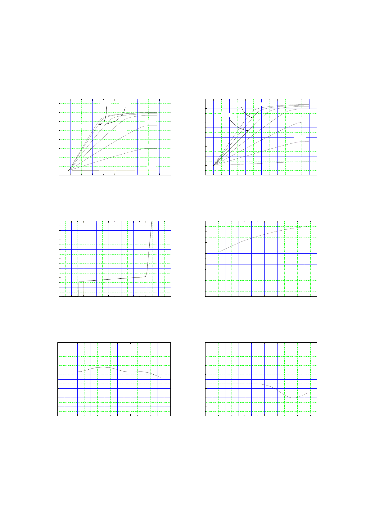
Typical Performance Characteristics
2.5 3.0 3.5 4.0 4.5
0.0
0.2
0.4
0.6
0.8
1.0
1.2
1.4
1.6
Vm1=2.5V
Vm1=2.0V
Vm1=1.5V
Vm1=1.0V
Vm1=0.5V
Vm1=3.0V
Vm1=0V
C.S. Threshold Voltage[V]
E.A. Output Voltage[V]
0.0 0.5 1.0 1.5 2.0 2.5 3.0
-0 . 2
0.0
0.2
0.4
0.6
0.8
1.0
1.2
1.4
Veao=3. 75V
Veao=3. 5V
Veao=4. 0V
Veao=3. 25V
Veao=3. 0V
Veao=2. 75V
Veao=2. 5V
C.S. Threshold Voltage[V]
Multiplier Input Voltage[V]
0 5 10 15 20 25 30 35 40 45
0.00
2.50m
5.00m
7.50m
10.00m
12.50m
15.00m
17.50m
20.00m
Supply Current[A]
Supply Voltage[V]
-20 0 20 40 60 80 100 120 140
2.45
2.46
2.47
2.48
2.49
2.50
2.51
2.52
Reference Voltage[V]
Temperature['C]
-20 0 20 40 60 80 100 120 140
9.4
9.5
9.6
9.7
9.8
9.9
10.0
10.1
10.2
Start-up Threshold[V]
Ambient Temperature['C]
-20 0 20 40 60 80 100 120 140
1.7
1.8
1.9
2.0
2.1
2.2
2.3
2.4
2.5
VU Lockout Hysteresis[V]
Ambient Temperature['C]
Figure 1. E.A. Output Voltage vs C.S. Thre shold
Figure 2. Multiplier Input Voltage vs C.S. Threshold
Figure 3. Supply Current vs Supply Voltage
Figure 4. Reference Voltage vs Temperature
Figure 5. Start-up Threshold vs Temperature
Figure 6. UV Lockout Hysteresis vs Temperature
 Loading...