Fairchild Semiconductor DM74LS75N, DM74LS75MX, DM74LS75M, DM74LS75CW Datasheet

© 2000 Fairchild Semiconductor Corporation DS006374 www.fairchildsemi.com
August 1986
Revised March 2000
DM74LS75 Quad Latch
DM74LS75
Quad Latch
General Description
These latches are idea lly suit ed for use as tempor ary sto rage for binary inform ation between processing units and
input/output or indicator units. Information present at a data
(D) input is transfe rred to t he Q outp ut when the enab le is
HIGH, and the Q output will follow the data input as long as
the enable remains HIGH. When the enable goes LOW, the
information (that was present at the data input at the time
the transition occur red ) is r eta ined at the Q output until the
enable is permitted to go HIGH.
These latches feature complementary Q and Q
outputs
from a 4-bit latch, and are available in 16-pin packages.
Ordering Code:
Devices also availab le in Tape and Reel. Specify by appending th e s uffix let t er “X” to the ordering code.
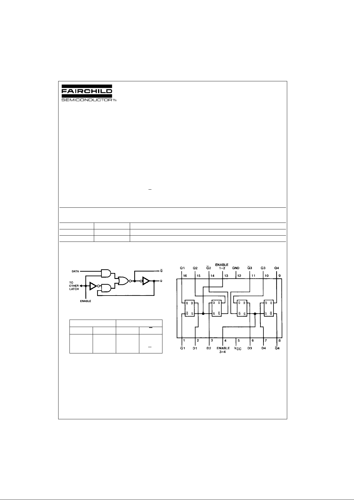
Logic Diagram
(Each Latch)
Function Table (Each Latch)
H = HIGH Level
L = LOW Level
X = Don't Care
Q
0
= The Level of Q Bef ore the HIGH-to-LOW Tran s iti on of ENABLE
Connection Diagram
Order Number Package Number Package Description
DM74LS75M M16A 16-Lead Small Outline Integrated Circuit (SOIC), JEDEC MS-012, 0.150 Narrow
DM74LS75N N16E 16-Lead Plastic Dual-In-Line Package (PDIP), JEDEC MS-001, 0.300 Wide
Inputs Outputs
D Enable Q Q
LHLH
HHHL
XLQ
0
Q
0

www.fairchildsemi.com 2
DM74LS75
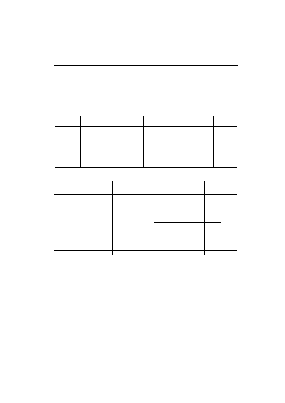
Absolute Maximum Ratings(Note 1)
Note 1: The “Absolute Maximum Ratin gs” are those v alues beyon d which
the safety of the dev ice cannot be guaranteed. T he device sh ould not be
operated at these limits. The parametric values defined in the Electrical
Characteristics tables are not guaranteed at the absolute maximum ratings.
The “Recommend ed O peratin g Cond itions” t able w ill defin e the co ndition s
for actual device operation.
Recommended Operating Conditions
Electrical Characteristics
over recommended operating free air temperature range (unless otherwise noted)
Note 2: All typicals are at VCC = 5V, TA = 25°C.
Note 3: Not more than one output should be shorted at a time, and the duration should not exceed one second.
Note 4: I
CC
is measured with all out puts open and all input s g rounded.
Note 5: T
A
= 25°C and VCC = 5V.
Supply Voltage 7V
Input Voltage 7V
Operating Free Air Temperature Range 0°C to +70°C
Storage Temperature Range −65°C to +150°C
Symbol Parameter Min Nom Max Units
V
CC
Supply Voltage 4.75 5 5. 25 V
V
IH
HIGH Level Input Voltage 2 V
V
IL
LOW Level Input Voltage 0.8 V
I
OH
HIGH Level Output Current −0.4 mA
I
OL
LOW Level Output Current 8 mA
t
W
Enable Pulse Width (Note 5) 20 ns
t
SU
Setup Time (Note 5) 20 ns
t
H
Hold Time (Note 5) 0 ns
T
A
Free Air Operating Temperature 0 70 °C
Symbol Parameter Conditions Min
Typ
Max Units
(Note 2)
V
I
Input Clamp Voltage VCC = Min, II = −18 mA −1.5 V
V
OH
HIGH Level VCC = Min, IOH = Max
2.7 3.5 V
Output Voltage VIL = Max, VIH = Min
V
OL
LOW Level VCC = Min, IOL = Max
0.35 0.5
Output Voltage VIL = Max, VIH = Min V
IOL = 4 mA, VCC = Min 0.25 0.4
I
I
Input Current @ Max VCC = Max, VI = 7V D 0.1
mA
Input Voltage Enable 0.4
I
IH
HIGH Level Input VCC = Max, VI = 2.7V D 20
µA
Current Enable 80
I
IL
LOW Level Input VCC = Max, VI = 0.4V D −0.4
mA
Current Enable −1.6
I
OS
Short Circuit Output Current VCC = Max (Note 2) −20 −100 mA
I
CC
Supply Current VCC = Max (Note 3) 6.3 12 mA
 Loading...