Fairchild Semiconductor DM74LS670N, DM74LS670MX, DM74LS670M, DM74LS670CW Datasheet

© 2000 Fairchild Semiconductor Corporation DS006436 www.fairchildsemi.com
August 1986
Revised March 2000
DM74LS670 3-STATE 4-by-4 Register File
DM74LS670
3-STATE 4-by-4 Register File
General Description
These register files are organized as 4 words of 4 bits
each, and separate on-chip decoding is provided for
addressing the four word locations to either write-in or
retrieve data. This permits writing into one location, and
reading from another word location, simultaneously.
Four data inputs are available to supply the word to be
stored. Location of the word is determined by the write
select inputs A and B, in conjunction with a write-enable
signal. Data applied at the inputs should be in its true form.
That is, if a high level signal is desired from the output, a
high level is applied at the data in put for tha t particular bit
location. The latch inputs a re arranged so that new data
will be accepted only if both internal addre ss gate inputs
are HIGH. When this condition exists, data at the D input is
transferred to the latch output. When the write-enable
input, G
W
, is HIGH, the data inputs are inhibited and their
levels can cause no change in the information stored in the
internal latches. W h en the r ead -enable input, G
R
, is HIGH,
the data outputs are inhibited an d go into the high impedance state.
The individual address lines permit direct acquisition of
data stored in any four of the latches. Four individual
decoding gates are used to co mple te th e ad dre ss for rea ding a word. When the read addre ss is ma de in con juncti on
with the read-enable sig nal, the word appears at the four
outputs.
This arrangement—data entry addressing separate from
data read addressin g and individual sense line — elimi-
nates recovery times, permits simultaneous reading and
writing, and is limited in speed only by the write time (27 ns
typical) and the read time (24 ns typica l). The register fi le
has a non-volatile readout in that data is not lost when
addressed.
All inputs (except read enable and w rite enable) are b uffered to lower th e driv e require ments to one no rmal Series
DM74LS load, and inpu t clamping diod es minimi ze switching transients to simplify system design. High spee d, double ended AND-OR-INVERT gat es are employed for the
read-address function and have high sink current, 3-STATE
outputs. Up to 128 of th ese o utp uts may be wire-AND connected for increa sing the capacity up to 5 12 words. Any
number of these regi sters may be parallel ed to provide nbit word length.
Features
■ For use as:
Scratch pad memory
Buffer storage between processors
Bit storage in fast multiplication designs
■ Separate read/write addressing permits simultaneous
reading and writing
■ Organized as 4 words of 4 bits
■ Expandable to 512 words of n-bits
■ 3-STATE versions of DM74LS170
■ Fast access times 20 ns typ
Ordering Code:
Devices also availab le in Tape and Reel. Specify by appending th e s uffix let t er “X” to the ordering code.
Order Number Package Number Package Description
DM74LS670M M16A 16-Lead Small Outline Integrated Circuit (SOIC), JEDEC MS-0 12, 0.150 Narrow
DM74LS670N N16E 16-Lead Plastic Dual-In-Line Package (PDIP), JEDEC MS-001, 0.300 Wide

www.fairchildsemi.com 2
DM74LS670
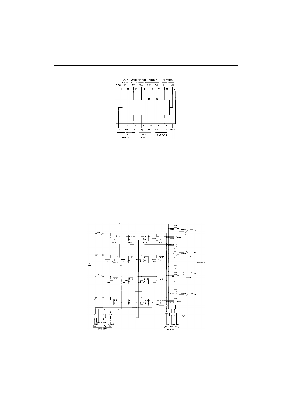
Connection Diagram
Function Tables
Write Table
(Note 1)(Note 2) Read Table (Note 3)
H = HIGH Level L = LOW Level X = Don’t Care Z = High Impedance (OFF)
Note 1: (Q = D) = The four selected inte rnal flip-flop outputs will assume the states app lied to the four external dat a inputs.
Note 2: Q
0
= The level of Q befo re t he indicated input cond iti ons were established .
Note 3: WOB1 = The first bit of word 0, etc.
Logic Diagram
Write Inputs Word
W
BWAGW
0123
LLLQ = DQ
0
Q
0
Q
0
LHL Q0Q = DQ0Q
0
HLL Q0Q0Q = DQ
0
HHL Q0Q
0
Q0Q = D
XXH Q
0
Q
0
Q
0
Q
0
Read Inputs Outputs
R
BRAGR
Q1 Q2 Q3 Q4
L L L WOB1 WOB2 WOB3 WOB4
L H L W1B1 W1B2 W1B3 W1B4
H L L W2B1 W2B2 W2B3 W2B4
H H L W3B1 W3B2 W3B3 W3B4
XXHZZZZ
 Loading...