

Fairchild Semiconductor DM74LS573WMX, DM74LS573WM, DM74LS573N Datasheet

© 2000 Fairchild Semiconductor Corporation DS009814 www.fairchildsemi.com
October 1988
Revised March 2000
DM74LS573 Octal D-Type Latch with 3-STATE Outputs
DM74LS573
Octal D-Type Latch with 3-STATE Outputs
General Description
The DM74LS573 is a high sp eed octal latch with buffer ed
common Latch Enable (LE) and buffered common Output
Enable (OE
) inputs.
This device is functionally identical to the DM74LS373, but
has different pinouts.
Features
■ Inputs and outputs on op posite sides of package allow ing easy interface with microprocessors
■ Useful as input or output port for microprocessors
■ Functionally identical to DM74LS373
■ Input clamp diodes limit high speed termination effects
■ Fully TTL and CMOS compatible
Ordering Code:
Devices also availab le in Tape and Reel. Specify by appending th e s uffix let t er “X” to the ordering code.
Logic Symbol
VCC = Pin 20
GND = Pin 10
Connection Diagram
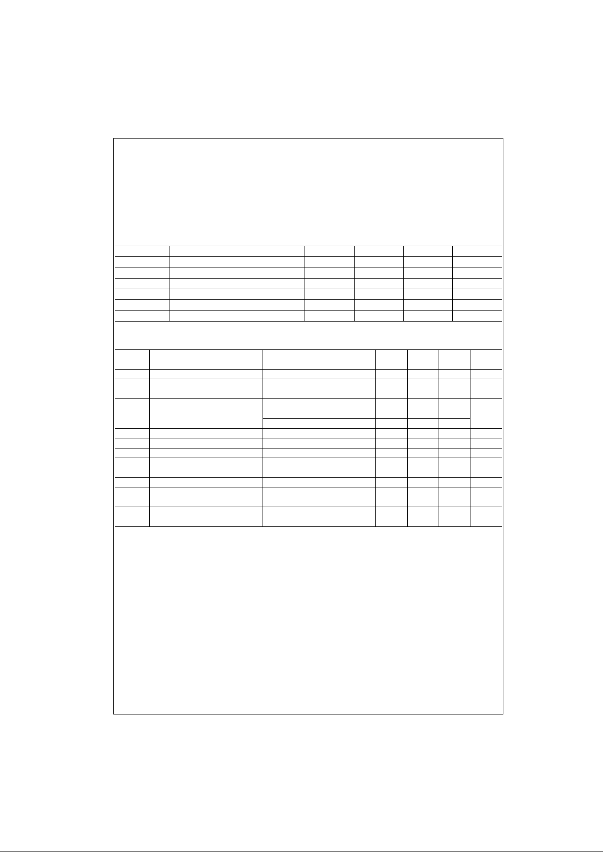
Pin Descriptions Function Tables
L = LOW State
H = HIGH State
X = Don't Care
Z = High Impedance St at e
QO = Previous Condit ion of O
Order Number Package Number Package Description
DM74LS573WM M20B 20-Lead Small Outline Integrated Circuit (SOIC), JEDEC MS-013, 0.300 Wide
DM74LS573N N20A 20-Lead Plastic Dual-In-Line Package (PDIP), JEDEC MS-001, 0.300 Wide
Pin Names Description
D0–D7 Data Inputs
LE Latch Enable Input (Active HIGH)
OE
3-STATE Output Enable Input (Active LOW)
O0–O7 3-STATE Latch Outputs
Output Latch
D
Output
Enable Enable O
LHHH
LHLL
LLXQ
O
HXXZ
www.fairchildsemi.com 2
DM74LS573
Absolute Maximum Ratings(Note 1)
Note 1: The “Absolute Maximum Ratin gs” are those v alues beyon d which
the safety of the dev ice cannot be guaranteed. T he device sh ould not be
operated at these limits. The parametric values defined in the Electrical
Characteristics tables are not guaranteed at the absolute maximum ratings.
The “Recommend ed O peratin g Cond itions” t able w ill defin e the co ndition s
for actual device operation.
Recommended Operating Conditions
Electrical Characteristics
Over recommended operating free air temperature range (unless otherwise noted)
Note 2: All typicals are at VCC = 5V, TA = 25°C.
Note 3: Not more than one output should be shorted at a time, and the duration should not exceed one second.
Supply Voltage 7V
Input Voltage 7V
Operating Free Air Temperature Range 0°C to +70°C
Storage Temperature Range −65°C to +150°C
Symbol Parameter Min Nom Max Units
V
CC
Supply Voltage 4.75 5 5.25 V
V
IH
HIGH Level Input Voltage 2 V
V
IL
LOW Level Input Voltage 0.8 V
I
OH
HIGH Level Input Current −2.6 mA
I
OL
LOW Level Output Current 24 mA
T
A
Free Air Operating Temperature 0 70 °C
Symbol Parameter Conditions Min
Typ
Max Units
(Note 2)
V
I
Input Clamp Voltage VCC = Min, II = −18 mA −1.5 V
V
OH
HIGH Level VCC = Min, IOH = Max,
2.7 3.4 V
Output Voltage VIL = Max
V
OL
LOW Level VCC = Min, IOL = Max,
0.35 0.5
Output Voltage VIH = Min V
IOL = 4 mA, VCC = Min 0.25 0.4
I
I
Input Current @ Max Input Voltage VCC = Max, VI = 7V 1 mA
I
IH
HIGH Level Input Current VCC = Max, VI = 2.7V 20 µA
I
IL
LOW Level Input Current VCC = Max, VI = 0.4V −0.4 mA
I
OS
Short Circuit VCC = Max
−30 −130 mA
Output Current (Note 3)
I
CC
Supply Current VCC = Max 50 mA
I
OZH
3-STATE Output VCC = V
CCH
20 µA
OFF Current HIGH V
OZH
= 2.7V
I
OZL
3-STATE Output VCC = V
CCH
−20 µA
OFF Current LOW V
OZL
= 0.4V
 Loading...