

Fairchild Semiconductor DM74LS534N Datasheet
March 1989
Revised March 2000
DM74LS534
Octal D-Type Flip-Flop with 3-STATE Outputs
General Description
The DM74LS534 is a high spee d, low power o ctal D-type
flip-flop featuring separate D-type inputs for each flip-flop
and 3-STATE outputs for bus oriented applications. A buffered Clock (CP) and Output Enable (OE
flip-flops. The DM74LS534 is the same as the DM74LS374
except that the outputs are inverted.
Ordering Code:
Order Number Package Number Package Description
DM74LS534N N20A 20-Lead Plastic Dual-In-Line Package (PDIP), JEDEC MS-001, 0.300 Wide
) is common to all
DM74LS534 Octal D-Type Flip-Flop with 3-STATE Outputs
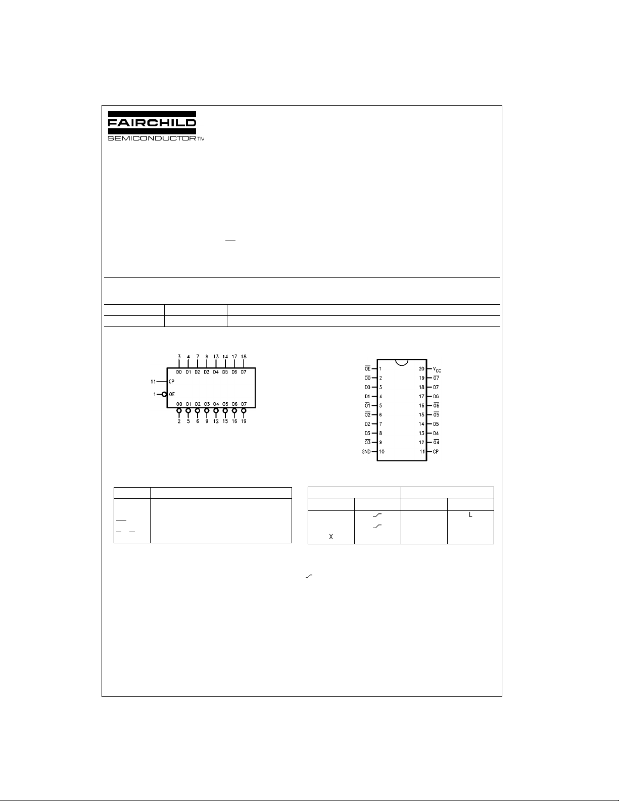
Logic Symbol
VCC = Pin 20
GND = Pin 10
Pin Descriptions
Pin Name Description
D0–D7 Data Inputs
CP Clock Pulse Input (Active Rising Edge)
OE
0–O7 Complementary 3-STATE Outputs
O
3-STATE Output Enable Input (Active LOW)
Connection Diagram
Truth Table
Inputs Outputs
D
n
H
L
XXHZ
H = HIGH Voltage Level
L = LOW Voltage Level
X = Immaterial
Z = High Impedance
= LOW-to-HIGH Clock (CP) transistion
CP OE
LL
LH
O
n
© 2000 Fairchild Semiconductor Corporation DS009812 www.fairchildsemi.com
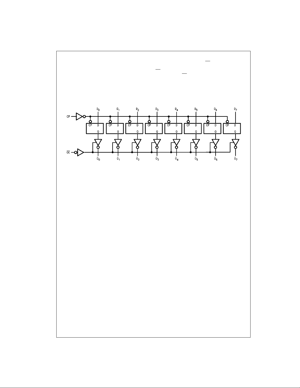
Functional Description
The DM74LS534 consis ts of eight edge- triggered flip-flops
with individual D-type inputs and 3-STATE true outputs.
The buffered clock and bu ffered Output Enable are common to all flip-flops. The eight flip-flops will store the state
of their individual D inp uts that meet the setup and hold
DM74LS534
times requirement s on the LOW- to-HIGH Clock ( CP) tran-
Logic Diagram
sistion. With the Output Ena ble (OE
the eight flip-flops are available at the outpu ts. When the
is HIGH, the outputs go to the high impedance state.
OE
Operation of the O E
flip-flops.
input does not affect the state of the
) LOW, the contents of
www.fairchildsemi.com 2
 Loading...