Fairchild Semiconductor DM74LS533WMX, DM74LS533WM, DM74LS533N Datasheet

© 2000 Fairchild Semiconductor Corporation DS009811 www.fairchildsemi.com
October 1988
Revised March 2000
DM74LS533 Octal Transparent Latch with 3-STATE Outputs
DM74LS533
Octal Transparent Latch with 3-STATE Outputs
General Description
The DM74LS533 consists of eight latches with 3-STATE
outputs for bus organized system applications. The flipflops appear transp arent to the data when Latch Enable
(LE) is HIGH. When LE is LOW, the data that meet s the
setup times is latched. Data appe ars on the bus when the
Output Enable (OE
) is LOW. When OE is HIGH the bus
output is in the h igh impeda nce state. Th e DM74LS53 3 is
the same as the DM74LS373, exce pt that the outputs are
inverted. For detailed specifications please see the
DM74LS373 data sheet, but note that the propagation
delays from data to output are 5.0 ns longer for the
DM74LS533 than for the DM74LS373.
Features
■ Eight latches in a single package
■ 3-STATE outputs for bus interfacing
Ordering Code:
Devices also availab le in Tape and Reel. Specify by appending th e s uffix let t er “X” to the ordering code.
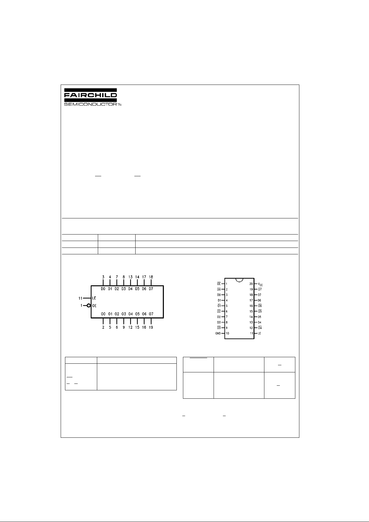
Logic Symbol
VCC = Pin 20
GND = Pin 10
Pin Descriptions
Connection Diagram
Function Table
L = LOW State
H = HIGH State
X = Don't Care
Z = High Impedance St at e
QO = Previous Condit ion of O
Order Number Package Number Package Description
DM74LS533WM M20B 20-Lead Small Outline Integrated Circuit (SOIC), JEDEC MS-013, 0.300 Wide
DM74LS533N N20A 20-Lead Plastic Dual-In-Line Package (PDIP), JEDEC MS-001, 0.300 Wide
Pin Names Description
D0, D7 Data Inputs
LE Latch Enable Input (Active HIGH)
OE
Output Enable Input (Active LOW)
O
0–O7 Complementary 3-STATE Outputs
OUTPUT Latch D Output
Enable Enable O
LHHL
LHLH
LLXQ
O
HXXZ

www.fairchildsemi.com 2
DM74LS533
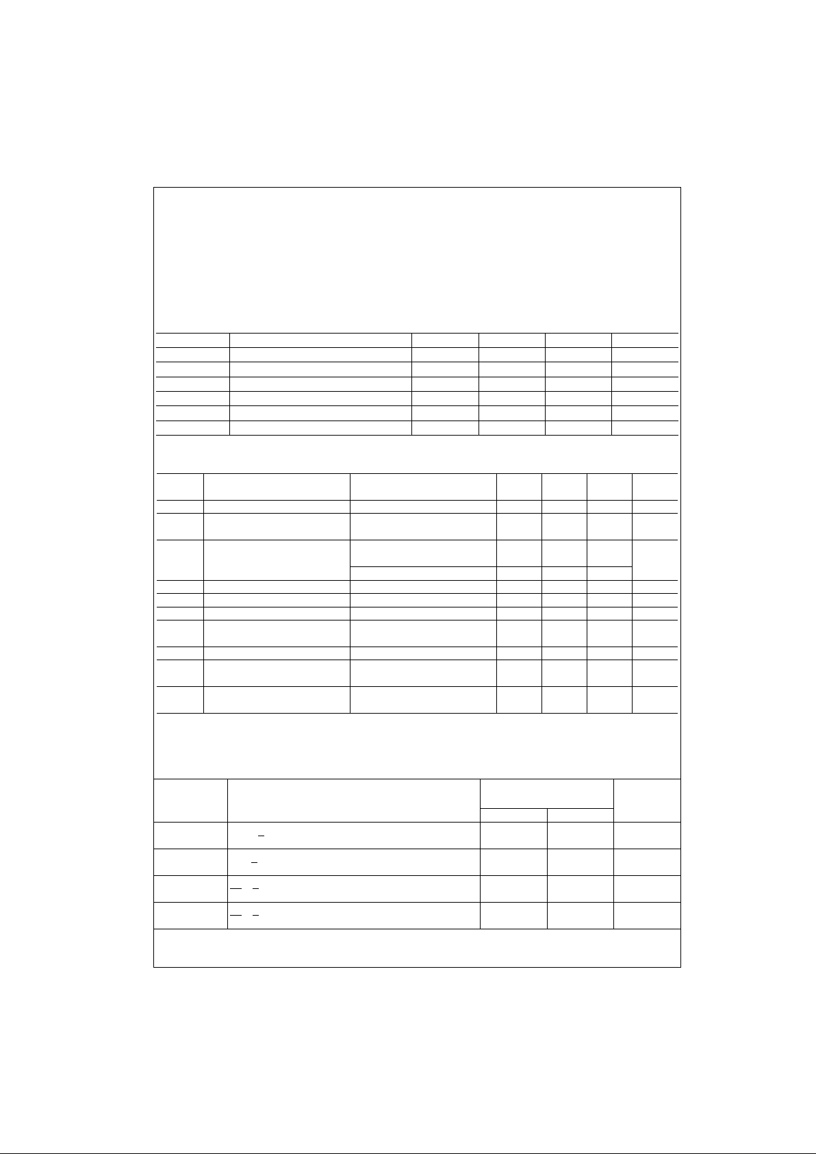
Absolute Maximum Ratings(Note 1)
Note 1: The “Absolute Maxi mum Rating s are those valu es beyond which
the safety of the dev ice cannot be guaranteed. T he device sh ould not be
operated at these limits. The parametric values defined in the Electrical
Characteristics tables are not guaranteed at the absolute maximum ratings.
The “Recommend ed O peratin g Cond itions” t able w ill defin e the co ndition s
for actual device operation.
Recommended Operating Conditions
Electrical Characteristics
Over recommended operating free air temperature range (unless otherwise noted)
Note 2: All typicals are at VCC = 5V, TA = 25°C.
Note 3: Not more than one output should be shorted at a time, and the duration should not exceed one second.
Switching Characteristics
VCC = +5.0V, TA = +25°C
Supply Voltage 7V
Input Voltage 7V
Operating Free Air Temperature Range 0°C to +70°C
Storage Temperature Range −65°C to +150°C
Symbol Parameter Min Nom Max Units
V
CC
Supply Voltage 4.75 5 5.25 V
V
IH
High Level Input Voltage 2 V
V
IL
Low Level Input Voltage 0.8 V
I
OH
High Level Output Current −2.6 mA
I
OL
Low Level Output Current 24 mA
T
A
Free Air Operating Temperature 0 70 °C
Symbol Parameter Conditions Min
Typ
Max Units
(Note 2)
V
I
Input Clamp Voltage VCC = Min, II = −18 mA −1.5 V
V
OH
HIGH Level VCC = Min, IOH = Max,
2.4 3.4 V
Output Voltage VIL = Max
V
OL
LOW Level VCC = Min, IOL = Max,
0.35 0.5
Output Voltage VIH = Min V
IOL = 12 mA, VCC = Min 0.4
I
I
Input Current @ Max Input Voltage VCC = Max, VI = 7V 0.1 mA
I
IH
HIGH Level Input Current VCC = Max, VI = 2.7V 20 µA
I
IL
LOW Level Input Current VCC = Max, VI = 0.4V −0.4 mA
I
OS
Short Circuit VCC = Max
−20 −100 mA
Output Current (Note 3)
I
CCZ
Supply Current VCC = Max 46 mA
I
OZL
3-STATE Output Off VCC = V
CCH
−20.0 µA
Current LOW V
OZL
= 0.4V
I
OZH
3-STATE Output Off VCC = V
CCH
20.0 µA
Current HIGH V
OZH
= 2.7V
CL = 50 pF
Symbol Parameter
RL = 2 kΩ
Units
Min Max
t
PLH
Propagation Delay 23
ns
t
PHL
Data to Q
x
23
t
PLH
Propagation Delay 30
ns
t
PHL
LE to Q
x
25
t
PZL
Output Enable Time 22
ns
t
PZH
OE to Q
x
20
t
PHZ
Output Enable Time 20
ns
t
PLZ
OE to Q
x
25
 Loading...