© 2000 Fairchild Semiconductor Corporation DS006305 www.fairchildsemi.com
October 1986
Revised April 2000
DM74AS286 9-Bit Parity Generator/Checker with Bus-Driver Parity I/O Port
DM74AS286
9-Bit Parity Generator/Checker
with Bus-Driver Parity I/O Port
General Description
These universal, 9-bit parity generators/checkers utilize
advanced Schottky high perfo rmance circuitry and fe ature
odd/even outputs to facilitate operation of either odd or
even parity applications. Th e word leng th capab ility is ea sily expanded by cascading.
The DM74AS286 can be used to upgrade the performance
of most systems utilizing the DM74AS280 parity generator/
checker. Although the DM74AS286 is implem ent ed w itho ut
expander inputs, the correspo nding funct ion is provid ed by
the availability of an input pin XMIT
. XMIT is a control line
which makes parity error outp ut active and parity an inp ut
port when HIGH; when LOW, parity error output is ina ctive
and parity becomes an output port. In additi on, parity I/O
control circuitry contains a fea ture to keep the I/O port in
the 3-STATE during power UP or DOWN to prevent bus
glitches.
Features
■ PNP inputs to reduce bus loading
■ Generates either odd or even parity for nine data lines
■ Inputs are buffered to lower the drive requirements
■ Can be used to upgrade existing systems using MSI
parity circuits
■ Cascadable for n-bits
■ Switching specifications at 50 pF
■ Switching specifications guaranteed over full
temperature and V
CC
range
■ A parity I/O portable to drive bus
Ordering Code:
Devices also availab le in Tape and Reel. Specify by appending th e s uffix let t er “X” to the ordering code.
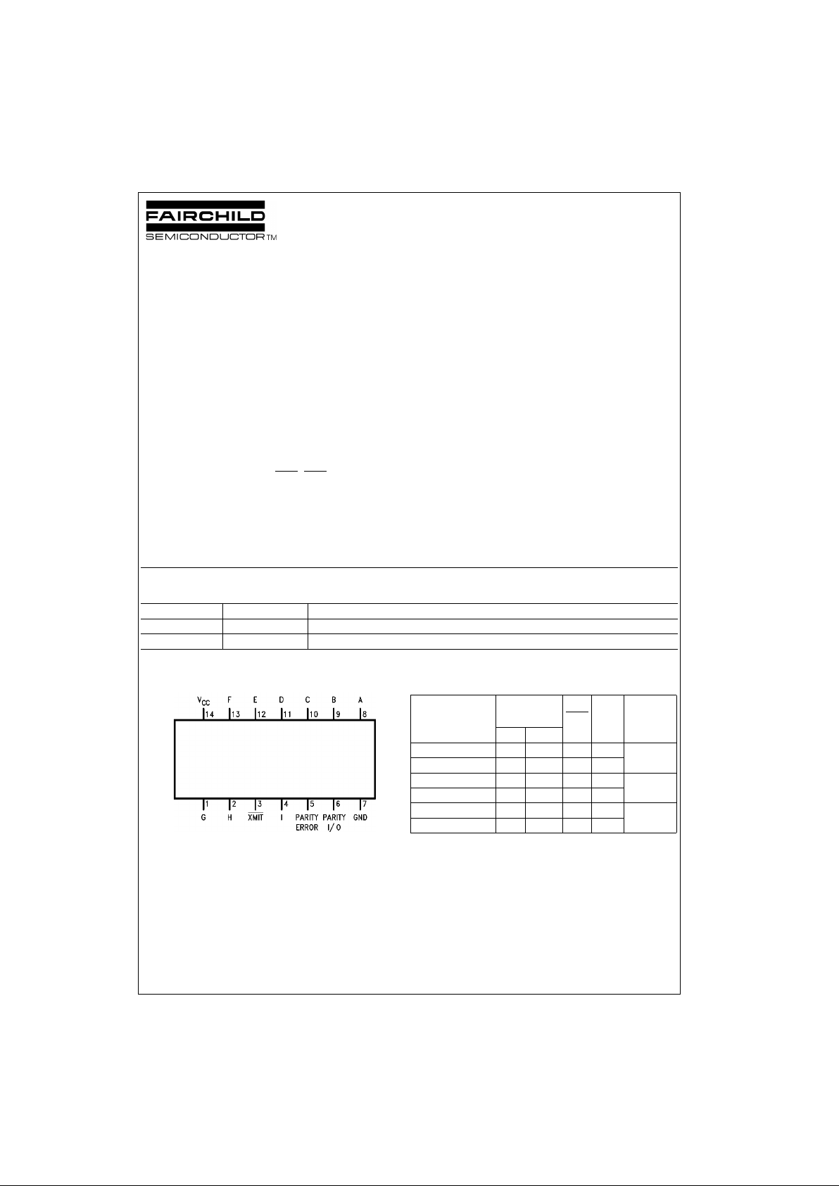
Connection Diagram Function Table
L = LOW Logic Level
H = HIGH Logic Level
N/A = Not Applicable
Order Number Package Number Package Description
DM74AS286M M14A 14-Lead Small Outline Integrated Circuit (SOIC), JEDEC MS-120, 0.150 Narrow
DM74AS286N N14A 14-Lead Plastic Dual-In-Line Package (PDIP), JEDEC MS-001, 0.300 Wide
Number of Inputs Parity I/O
XMIT
Parity
Error
Mode
(A thru I) of
that are HIGH Input Output Operation
0, 2, 4, 6, 8 N/A H L H Parity
1, 3, 5, 7, 9 N/A L L H Generator
0, 2, 4, 6, 8 H N/A H H Parity
0, 2, 4, 6, 8 L N/A H L Checker
1, 3, 5, 7, 9 H N/A H L Parity
1, 3, 5, 7, 9 L N/A H H Checker

www.fairchildsemi.com 2
DM74AS286
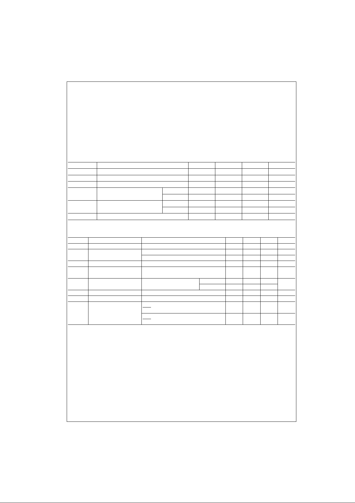
Absolute Maximum Ratings(Note 1)
Note 1: The “Absolute Maximum Ratings” are those values beyon d which
the safety of the dev ice cannot be guaranteed. T he device sh ould not be
operated at these limit s. The parametric values defin ed in the Electrical
Characteristics tables are not guaranteed at the absolute maximum ratings.
The “Recomme nded O peratin g Cond itions ” table will defin e the condition s
for actual device operation.
Recommended Operating Conditions
Electrical Characteristics
over recommended free-air temperature range. All typical values are measured at V
CC
= 5V, T
A
= 25°C.
Note 2: For I/O ports, the p a r ameters IIH and IIL include the OFF-state current, I
OZH
and I
OZL
.
Supply Voltage 7V
Input Voltage 7V
Operating Free Air Temperature Range 0°C to +70°C
Storage Temperature Range −65°C to +150°C
Typical θ
JA
N Package 77.0°C/W
M Package 108.0°C/W
Symbol Parameter Min Typ Max Units
V
CC
Supply Voltage 4.5 5 5.5 V
V
IH
HIGH Level Input Voltage 2 V
V
IL
LOW Level Input Vo ltage 0.8 V
I
OH
HIGH Level Output Current Parity I/O −15 mA
Parity Error −2mA
I
OL
LOW Level Output Current Parity I/O 48 mA
Parity Error 20 mA
T
A
Operating Free-Air Temperature 0 70 °C
Symbol Parameter Conditions Min Typ Max Units
V
IK
Input Clamp Voltage VCC = 4.5V, IIN = −18 mA −1.2 V
V
OH
HIGH Level IOH = Max, VCC = 4.5V 2.4 3.2 V
Output Voltage V
CC
= 4.5V to 5.5V, IOH = −2 mA VCC − 2V
V
OL
LOW Level Output Voltage VCC = 4.5V, IOL = Max 0.35 0.5 V
I
I
Input Current at Maximum VCC = 5.5V, VIH = 7V
0.1 mA
Input Voltage (V
I
= 5.5V for Parity I/O)
I
IH
HIGH Level Input Current VCC = 5.5V Others 20
µA
VIH = 2.7V (Note 2) Parity I/O 50
I
IL
LOW Level Input Current VCC = 5.5V, VIL = 0.4V (Note 2) −0.5 mA
I
O
Output Drive Current VCC = 5.5V, V
OUT
= 2.25V −30 −112 mA
I
CC
Supply Current VCC = 5.5V, Transmit Mode
43 mA
XMIT
= LOW
Receive Mode
50 mA
XMIT
= HIGH

3 www.fairchildsemi.com
DM74AS286
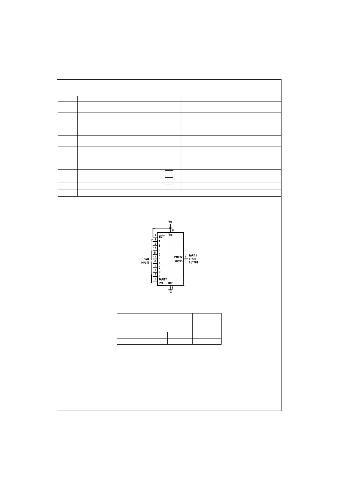
Switching Characteristics
over recommended supply and temperature range
Typical Applications
FIGURE 1. Dedicated 10-Bit Parity Sensing Configuration
Symbol Parameter From To Min Max Units
t
PLH
Propagation Delay Time
Any Data Input Parity I/O 3 15 ns
from LOW-to-HIGH Level Output
t
PHL
Propagation Delay Time
Any Data Input Parity I/O 3 14 ns
from HIGH-to-LOW Level Output
t
PLH
Propagation Delay Time
Any Data Input Parity Error 3 16.5 ns
from LOW-to-HIGH Level Output
t
PHL
Propagation Delay Time
Any Data Input Parity Error 3 16.5 ns
from HIGH-to-LOW Level Output
t
PLH
Propagation Delay Time
Parity I/O Parity Error 3 9 ns
from LOW-to-HIGH Level Output
t
PHL
Propagation Delay Time
Parity I/O Parity Error 3 9 ns
from HIGH-to-LOW Level Output
t
PZL
Output Enable Time to LOW Level XMIT Parity I/O 3 16 ns
t
PLZ
Output Disable Time from LOW Level XMIT Parity I/O 3 10 ns
t
PZH
Output Disable Time from HIGH Level XMIT Parity I/O 3 13 ns
t
PHZ
Output Enable Time to HIGH Level XMIT Parity I/O 3 11.5 ns
Number of Parity
Inputs that Result
are Logic “1” Output
0, 2, 4, 6, 8, 10 Even L
1, 3, 5, 7, 9 Odd H
 Loading...