

Fairchild Semiconductor CD4016BCN, CD4016BCMX, CD4016BCM Datasheet
November 1983
Revised January 1999
CD4016BC Quad Bilateral Switch
© 1999 Fairchild Semiconductor Corporation DS005661.prf www.fairchildsemi.com
CD4016BC
Quad Bilateral Switch
General Description
The CD4016BC is a quad bilate ral switch intended for the
transmission or multiplexing of analog or digital signals. It is
pin-for-pin compatible with CD4066BC.
Features
■ Wide supply voltage range: 3V to 15V
■ Wide range of digital and analog switching: ±7.5 V
PEAK
■ “ON” resistance for 15V operation: 400Ω (typ.)
■ Matched “ON” resistance over 15V signal input:
∆R
ON
= 10Ω (typ.)
■ High degree of linearity:
0.4% distortion (typ.)
@ f
IS
= 1 kHz, V
IS
= 5 V
p-p
,
V
DD−VSS
= 10V, RL = 10 kΩ
■ Extremely low “OFF” switch leakage:
0.1 nA (typ.)
@ V
DD
− V
SS
= 10V
T
A
= 25°C
■ Extremely high control input impedance: 10
12
Ω (typ.)
■ Low crosstalk between switches:
−50 dB (typ.)
@ f
IS
= 0.9 MHz, RL = 1 kΩ
■ Frequency response, switch “ON”: 40 MHz (typ.)
Applications
• Analog signal switching/multiplexing
Signal gating
Squelch control
Chopper
Modulator/Demodulator
Commutating switch
• Digital signal switching/multiplexing
• CMOS logic implementation
• Analog-to-digital/digital-to-analog conversion
• Digital control of frequency, impedance, phase, and ana-
log-signal gain
Ordering Code:
Devices also available in Tape and Reel. Specify by appending the letter suffix “X” to t he ordering code.
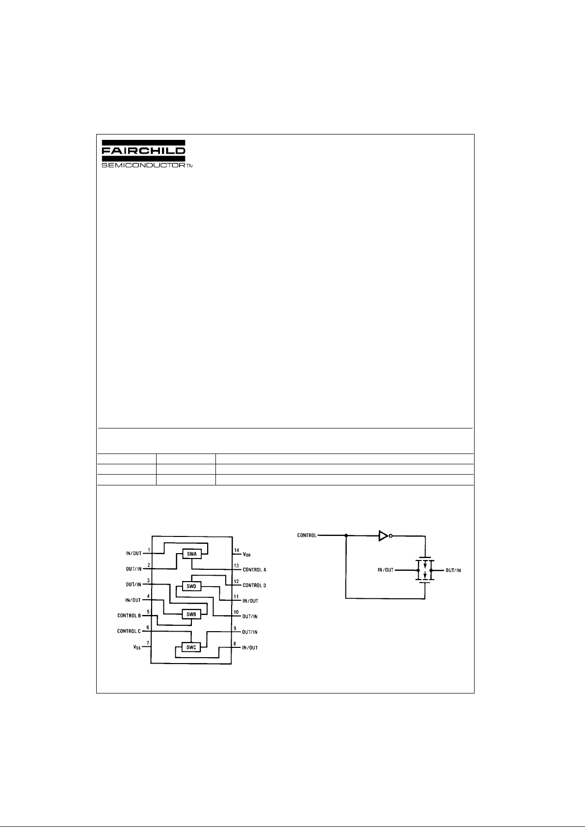
Connection Diagram
Pin Assignments for DIP and SOIC
Schematic Diagram
Order Number Package Number Package Description
CD4016BCM M14A 14-Lead Small Outline Integrated Circuit (SOIC), JEDEC MS-120, 0.150” Narrow
CD4016BCN N14A 14-Lead Plastic Dual-In-Line Package (PDIP), JEDEC MS-001, 0.300” Wide
www.fairchildsemi.com 2
CD4016BC
Absolute Maximum Ratings(Note 1)
(Note 2)
Recommended Operating
Conditions
(Note 2)
Note 1: “Absolute Maxi mum Ratings” are those valu es beyond which the
safety of the device cannot be guaranteed. They are not meant to imply
that the devices should be o perated at these lim its. The table s of “Recom mended Operating Conditions” and “Electrical Cha rac t eristics” provide conditions for actual device operation.
Note 2: V
SS
= 0V unless otherwis e specified.
DC Electrical Characteristics (Note 2)
Note 3: If the switch input is held at VDD, V
IHC
is the contro l input level that will cause the switch out put to meet the standard “B” s eries VOH and IOH output
levels. If the analog switch input is connected to V
SS
, V
IHC
is the control input level — which allows the switch to sink standard “B” series |IOH|, high level cur-
rent, and still maint ain a V
OL
≤ “B” series. These c urrents are shown in Figur e 8.
VDD Supply Voltage −0.5V to +18V
V
IN
Input Voltage −0.5V to VDD + 0.5V
T
S
Storage Temperature Range −65°C to + 150°C
Power Dissipation (P
D
)
Dual-In-Line 700 mW
Small Outline 500 mW
Lead Temperature
(Soldering, 10 seconds) 260°C
V
DD
Supply Voltage 3V to 15V
V
IN
Input Voltage 0V to V
DD
TA Operating Temperature Range −40°C to +85°C
Symbol Parameter Conditions
−40°C25°C +85°C
Units
Min Max Min Typ Max Min Max
I
DD
Quiescent Device V
DD
= 5V, VIN = VDD or V
SS
1.0 0.01 1.0 7.5 µA
Current V
DD
= 10V, V
IN
= VDD or V
SS
2.0 0.01 2.0 15 µA
V
DD
= 15V, VIN = VDD or V
SS
4.0 0.01 4.0 30 µA
Signal Inputs and Outputs
R
ON
“ON” Resistance RL = 10kΩ to (VDD − VSS)/2
VC = VDD, V
IS
= VSS or V
DD
V
DD
= 10V 610 275 660 840 Ω
V
DD
= 15V 370 200 400 520 Ω
RL = 10kΩ to (VDD − VSS)/2
VC = V
DD
V
DD
= 10V, V
IS
= 4.75 to 5.25V 1900 850 2000 2380 Ω
V
DD
= 15V, V
IS
= 7.25 to 7.75V 790 400 850 1080 Ω
∆R
ON
∆“ON” Resistance RL = 10kΩ to (VDD − VSS)/2
Between any 2 of VC = VDD, V
IS
= VSS to V
DD
4 Switches V
DD
= 10V 15 Ω
(In Same Package) V
DD
= 15V 10 Ω
I
IS
Input or Output VC = 0, VDD = 15V ±50 ±0.1 ±50 ±200 nA
Leakage V
IS
= 0V or 15V,
Switch “OFF” V
OS
= 15V or 0V
Control Inputs
V
ILC
LOW Level Input V
IS
= VSS and V
DD
Voltage V
OS
= VDD and V
SS
I
IS
= ±10 µA
V
DD
= 5V 0.9 0.7 0.4 V
V
DD
= 10V 0.9 0.7 0.4 V
V
DD
= 15V 0.9 0.7 0.4 V
V
IHC
HIGH Level Input V
DD
= 5V 3.5 3.5 3.5 V
Voltage V
DD
= 10V 7.0 7.0 7.0 V
V
DD
= 15V 11.0 11.0 11.0 V
(Note 3) and Figure 8
I
IN
Input Current V
CC
− V
SS
= 15V ±0.3 ±10−5±0.3 ±1.0 µA
V
DD
≥ V
IS
≥ V
SS
V
DD
≥ VC ≥ V
SS
3 www.fairchildsemi.com
CD4016BC
AC Electrical Characteristics (Note 4)
T
A
= 25°C, tr = tf = 20 ns and V
SS
= 0V unless otherwise specified
Note 4: AC Parameters are guaranteed by DC correlated testing.
Note 5: These devices should not be connected to circuits with the power “ON”.
Note 6: In all cases, th ere is approximately 5 p F of probe and jig capacit ance on the output; how ever, this capacitance is included in C
L
wherever it is specified.
Note 7: V
IS
is the voltage at the in/out pin and VOS is the voltage at the out/in pi n. VC is the voltage at the contro l input.
Symbol Parameter Conditions Min Typ Max Units
t
PHL
, t
PLH
Propagation Delay Time VC = VDD, CL = 50 pF, (Figure 1)
Signal Input to Signal Output RL = 200k
V
DD
= 5V 58 100 ns
VDD= 10V 27 50 ns
V
DD
= 15V 20 40 ns
t
PZH
, t
PZL
Propagation Delay Time RL = 1.0 kΩ, CL = 50 pF, (Figure 2, Figure 3)
Control Input to Signal V
DD
= 5V 20 50 ns
Output HIGH Impedance to VDD = 10V 18 40 ns
Logical Level V
DD
= 15V 17 35 ns
t
PHZ
, t
PLZ
Propagation Delay Time RL = 1.0 kΩ, CL = 50 pF, (Figure 2, Figure 3)
Control Input to Signal V
DD
= 5V 15 40 ns
Output Logical Level to V
DD
= 10V 11 25 ns
HIGH Impedance V
DD
= 15V 10 22 ns
Sine Wave Distortion VC = V
DD
= 5V, VSS = −50.4%
RL = 10 kΩ, V
IS
= 5 V
P-P
, f = 1 kHz,
(Figure 4)
Frequency Response — Switch VC = V
DD
= 5V, V
SS
= −5V, 40 MHz
“ON” (Frequency at −3 dB) RL = 1 kΩ, V
IS
= 5 V
P-P
,
20 Log10 VOS/VOS (1 kHz) −dB,
(Figure 4)
Feedthrough — Switch “OFF” V
DD
= 5V, VC = V
SS
= −5V, 1.25 MHz
(Frequency at −50 dB) RL = 1 kΩ, V
IS
= 5 V
P-P
,
20 Log10 (VOS/VIS) = −50 dB,
(Figure 4)
Crosstalk Between Any T wo V
DD
= V
C(A)
= 5V; V
SS
= V
C(B)
= −5V, 0.9 MHz
Switches (Frequency at −50 dB) RL = 1 kΩV
IS(A)
= 5 V
P-P
,
20 Log10 (V
OS(B)/VOS(A)
) = −50 dB,
(Figure 5)
Crosstalk; Control Input to V
DD
= 10V, RL = 10 kΩ 150 mV
P-P
Signal Output R
IN
= 1 kΩ, VCC = 10V Square Wave,
CL = 50 pF (Figure 6)
Maximum Control Input RL = 1 kΩ, CL = 50 pF, (Figure 7)
V
OS(f)
= ½ VOS(1 kHz)
V
DD
= 5V 6.5 MHz
V
DD
= 10V 8.0 MHz
V
DD
= 15V 9.0 MHz
C
IS
Signal Input Capacitance 4pF
C
OS
Signal Output Capacitance V
DD
= 10V 4 pF
C
IOS
Feedthrough Capacitance VC = 0V 0.2 pF
C
IN
Control Input Capacitance 57.5 pF
 Loading...