

Fairchild Semiconductor BC212L Datasheet
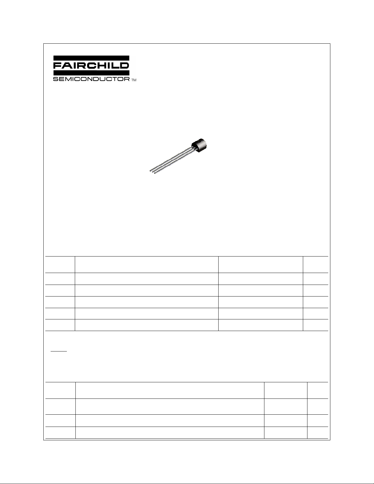
BC212L
BC212L
B
C
E
TO-92
PNP General Purpose Amplifier
This device is designed for general purpose amplifier applications at collector currents to 300mA.
Sourced from Process 68.
Absolute Maximum Ratings* T
ParameterSymbol
V
CEO
V
CBO
V
EBO
I
C
T
J, Tstg
*These ratings are limiting values above which the serviceability of any semiconductor device may be impaired.
A
= 25°C unless otherwise noted
Value
Units
V50Collector-Emitter Voltage
V60Collector-Base Voltage
V5Emitter-Base Voltage
mA300Collector Current - Continuous
°C-55 to +150Operating and Storage Junction Temperature Range
NOTES:
1) These ratings are based on a maximum junction temperature of 150°C.
2) These are steady state limits. The factory should be consulted on applications involving pulsed or low duty cycle operations.
Thermal Characteristics T
Symbol
P
D
R
θJC
R
θJA
2000 Fairchild Semiconductor International Rev. A 7/24/00
Total Device Dissipation
Derate above 25°C
A
= 25°C unless otherwise noted
MaxCharacteristic
625
5.0
Units
mW
mW/°C
°C/W83.3Thermal Resistance, Junction to Case
°C/W200Thermal Resistance, Junction to Ambient
PNP General Purpose Amplifier
BC212L
(continued)
Electrical Characteristics
ParameterSymbol
OFF CHARACTERISTICS
BV
CEO
BV
CBO
BV
EBO
I
CBO
I
EBO
ON CHARACTERISTICS*
h
FE
V
CE(sat)
V
BE(sat)
V
BE(on)
Collector-Emitter Breakdown Voltage
Collector-Base Breakdown Voltage
Emitter-Base Breakdown Voltage
Collector Cutoff Current
Emitter Cutoff Current
DC Current Gain
Collector-Emitter Saturation Voltage
Base-Emitter Saturation Voltage
Base-Emitter On Voltage
T
A
= 25°C unless otherwise noted
I
= 2 mA
C
I
= 10 µA
C
I
= 10 µA
E
V
CB
V
EB
= 10 uA, VCE = 5 V
I
C
I
= 2 mA, VCE = 5 V
C
I
= 100 mA, IB = 5 mA
C
I
= 100 mA, IB = 5 mA
C
= 2 mA, VCE = 5 V
I
C
= 30V
= 4V
MinTest Conditions
UnitsMax
V50
V60
V5
nA15
nA15
40
300
60
V0.6
V1.1
V0.720.6
SMALL SIGNAL CHARACTERISTICS
C
ob
h
fe
Output Capacitance
Small Signal Current Gain
Noise FigureNF
V
= 10 V, f = 1.0 MHz
CB
= 2 mA,VCE = 5 V, f=1kHz
I
C
= 200 uA,VCE = 5 V, f=1kHz,
I
C
pF10
-60
dB10
Rg=2KOhms,BW=200Hz
MHz200VCE=5V, IC=10mA,f=100MHzCurrent Gain-Bandwidth ProductfT
*Pulse Test: Pulse Width < 300µs, Duty Cycle < 2.0%
__________________________________________________________________________________
Rev. A 7/24/00
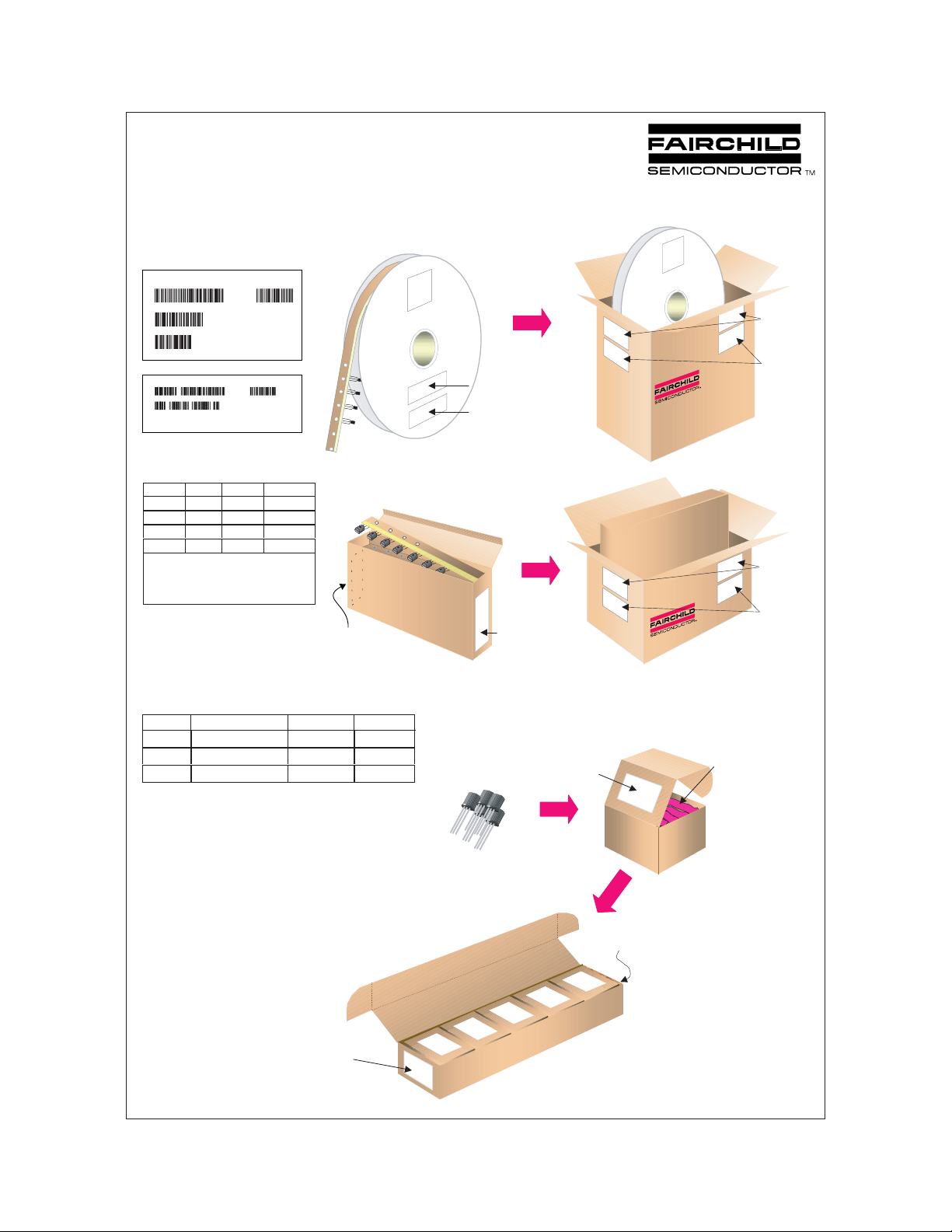
TO-92 Tape and Reel Data and Package Dimensions
TO-92 Packaging
Configuration: Figure 1.0
FSCINT Label sample
FAIRCHILD SEMICONDUCTOR CORPORATION
LOT:
CBVK741B019
NSID:
PN2222N
D/C1:
SPEC REV:
D9842
QA REV:
HTB:B
QTY:
10000
SPEC:
B2
(FSCINT)
F63TNR Label sample
LOT: CBVK741B019
FSID: PN222N
D/C1: D9842 QTY1: SPEC REV:
D/C2: QTY2: CPN:
QTY: 2000
SPEC:
N/F: F (F63TNR)3
TO-92 TNR/AMMO PACKING INFROMATION
Packing Style Quantity EOL code
Reel A 2,000 D26Z
Ammo M 2 ,000 D74Z
Unit w eight = 0.22 gm
Reel weight w ith components = 1.04 kg
Amm o weight with comp onents = 1.02 kg
Max q uantity pe r intermediate box = 10,000 units
E2,000 D27Z
P2,000 D75Z
(TO-92) BULK PACKING INFORMATION
EOL
CODE
J18Z
J05Z
NO EOL
CODE
DESCRIPTION
TO-18 OPTION STD NO LEAD CLIP
TO-5 OPTION STD NO LEAD CLIP
TO-92 STANDARD
STRAIGHT
NO LEADCLIP
LEADCLIP
DIMENSION
327mm x 158mm x 135mm
Immediate Box
Customized
Label
QUANTITY
2.0 K / BOX
1.5 K / BOX
2.0 K / BOX
TAPE and REEL OPTION
See Fig 2.0 for various
Reeling Styles
5 Reels per
Intermediate Box
F63TNR
Label
Customized
Label
AMMO PACK OPTION
See Fig 3.0 for 2 Ammo
Pack Options
5 Ammo boxes per
Intermediate Box
F63TNR
Label
BULK OPTION
See Bulk Packing
Information table
FSCINT Label
375mm x 267mm x 375mm
Intermediate Box
333mm x 231mm x 183mm
Intermediate Box
Anti-static
Bubble Sheets
FSCINT
Label
Customized
Label
FSCINT
Label
Customized
Label
FSCINT Label
530mm x 130mm x 83mm
Intermediate box
2000 units per
EO70 box for
std option
C
Label
10,000 units maximum
per intermediate box
for std option
ustomized
5 EO70 boxes per
intermediate Box
114mm x 102mm x 51mm
Immediate Box
September 1999, Rev. B
 Loading...