

Fairchild Semiconductor 74ACTQ273SJX, 74ACTQ273SCX, 74ACTQ273SC, 74ACTQ273PC, 74ACTQ273MTCX Datasheet
...
© 1999 Fairchild Semiconductor Corporation DS010585 www.fairchildsemi.com
August 1989
Revised November 1999
74ACTQ273 Quiet Series Octal D-Type Flip-Flop
74ACTQ273
Quiet Series Octa l D-Type Flip-Flop
General Description
The ACTQ273 has eight edge-triggered D-type flip-flops
with individual D inputs and Q outputs . The common buffered Clock (CP) and Mast er Reset (MR
) input load and
reset (clear) all flip-flops simultaneously.
The register is fu lly edge-triggered. The sta te of each D-
type input, one setu p time before th e LOW-to-HIGH clock
transition, is transferre d to the corresponding flip- flop’s Q
output.
All outputs will be forced LOW indepe ndently of Clock or
Data inputs by a LOW voltage level on the MR
input. The
device is useful fo r app licati ons where the tr ue ou tput only
is required and the Clock and Master Reset are common to
all storage elements.
The ACTQ utilizes Fairchild Quiet Series technology to
guarantee quiet output switching and improved dynamic
threshold performance. FACT Quiet Series features
GTO output control and unde rshoot corre ctor in add ition
to a split ground bus for superior performance.
Features
■ ICC reduced by 50%
■ Guaranteed simultaneous switching noise level and
dynamic threshold performan ce
■ Guarante ed pin-to-pin skew AC performance
■ Improved latch-up immunity
■ Buffered common clock and asynchronous master reset
■ Outputs source/sink 24 mA
■ 4 kV minimum ESD immunity
Ordering Code:
Device also available in Tape and Reel. Specify by appending suffix letter “X” to the ordering code.
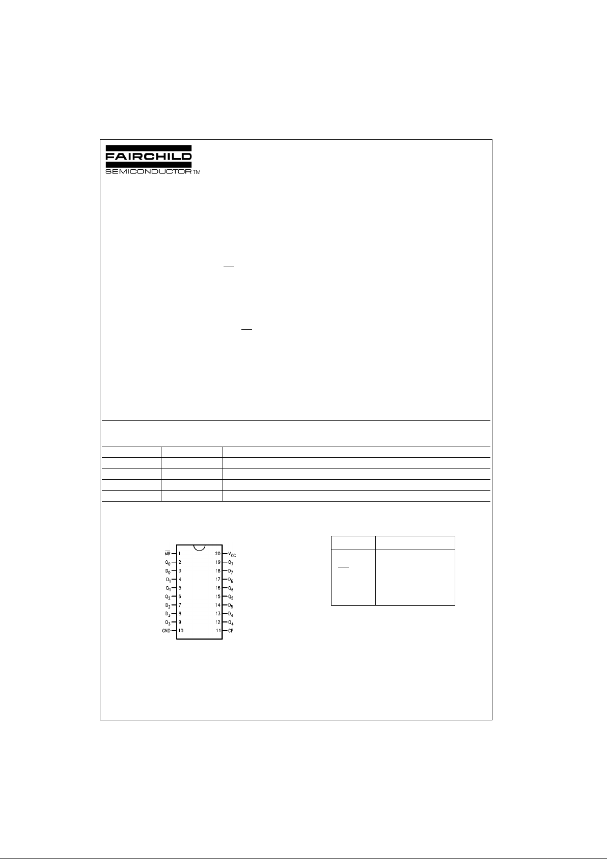
Connection Diagram Pin Descriptions
FACT, FACT Quiet Series, and GTO are trademarks of F airchild Semiconductor Corporation.
Order Number Package Number Package Description
74ACTQ273SC M20B 20-Lead Small Outline Integrated Circuit, JEDEC MS-013, 0.300” Wi d e Body
74ACTQ273SJ M20D 20-Lead Small Outline Package, EIAJ TYPE II, 5.3mm Wide
74ACTQ273MTC MTC20 20-Lead Thin Shrink Small Outline Package (TSSOP), JEDEC MO-153, 4.4mm Wide
74ACTQ273PC N20A 20-Lead Plastic Dual-In-L ine Pa ckag e, JED EC MS-0 01 , 0.300 ” Wide
Pin Names Description
D
0–D7
Data Inputs
MR
Master Reset
CP Clock Pulse Input
Q
0–Q7
Data Outputs

www.fairchildsemi.com 2
74ACTQ273
Logic Symbols
IEEE/IEC
Mode Select-Function Table
H = HIGH Voltage Level
L = LOW Voltage Level
X = Immaterial
= LOW-to-HIGH Transitio n
Logic Diagram
Please note that this diagram is provided only for the understanding of logic operations and should not be used to estimate propagation delays.
Operating Mode
Inputs Outputs
MR
CP D
n
Q
n
Reset (Clear) L X X L
Load “1” H
H H
Load “0” H
L L

3 www.fairchildsemi.com
74ACTQ273
Absolute Maximum Ratings(Note 1) Recommended Operating
Conditions
Note 1: Absolute max imum ratings are those values beyond whi c h damage
to the device may occu r. The databook spe cificatio ns shou ld be met, wit hout exception, to ensure that the system de sign is relia ble over its p ower
supply, temperature, and output/input loading variables. Fairchild does not
recommend operation of FACT circ uit s outside databook spec if ic at ions.
DC Electrical Characteristics
Note 2: All outputs loaded; thres holds on input associate d w it h output under test.
Note 3: Maximum test duration 2.0 ms, one output loaded at a time.
Note 4: Max number of outputs defined as (n). n − 1 Data inputs are driven 0V to 3V; one output @ GND.
Note 5: Max number of Data Inputs (n) switching. (n − 1) In puts switching 0V to 3V (ACTQ). Input-under-test switching: 3V to threshold (V
ILD
), 0V to thresh-
old (V
IHD
) f = 1 MHz.
Supply Voltage (VCC) −0.5V to +7.0V
DC Input Diode Current (I
IK
)
V
I
= −0.5V −20 mA
V
I
= VCC + 0.5V +20 mA
DC Input Voltage (V
I
) −0.5V to VCC + 0.5V
DC Output Diode Current (I
OK
)
V
O
= −0.5V −20 mA
V
O
= VCC + 0.5V +20 mA
DC Output Voltage (V
O
) −0.5V to VCC + 0.5V
DC Output Source
or Sink Current (I
O
) ±50 mA
DC V
CC
or Ground Current
per Output Pin (I
CC
or I
GND
) ±50 mA
Storage Temperature (T
STG
) −65°C to +150°C
DC Latch-up Source or
Sink Current ±300 mA
Junction Temperature (T
J
)
PDIP 140°C
Supply Voltage (V
CC
) 4.5V to 5.5V
Input Voltage (V
I
) 0V to V
CC
Output Voltage (VO) 0V to V
CC
Operating Temperature (TA) −40°C to +85°C
Minimum Input Edge Rate ∆V/∆t
V
IN
from 0.8V to 2.0V
V
CC
@ 4.5V, 5.5V 125 mV/ns
Symbol Parameter
V
CC
TA = +25°C TA = −40°C to +85°C
Units Conditions
(V) Typ Guaranteed Limits
V
IH
Minimum HIGH Level 4.5 1.5 2.0 2.0
V
V
OUT
= 0.1V
Input Voltage 5.5 1.5 2.0 2.0 or VCC − 0.1V
V
IL
Maximum LOW Level 4.5 1.5 0.8 0.8
V
V
OUT
= 0.1V
Input Voltage 5.5 1.5 0.8 0.8 or VCC − 0.1V
V
OH
Minimum HIGH Level 4.5 4.49 4.4 4.4
VI
OUT
= −50 µA
Output Voltage 5.5 5.49 5.4 5.4
V
IN
= V
IL
or V
IH
4.5 3.86 3.76 V IOH = −24 mA
5.5 4.86 4.76 IOH = −24 mA (Note 2)
V
OL
Maximum LOW Level 4.5 0.001 0.1 0.1
VI
OUT
= 50 µA
Output Voltage 5.5 0.001 0.1 0.1
VIN = V
IL
or V
IH
4.5 0.36 0.44 V IOL = 24 mA
5.5 0.36 0.44 I
OL
= 24 mA (Note 2)
I
IN
Maximum Input Leakage Current 5.5 ±0.1 ± 1.0 µAVI = VCC, GND
I
CCT
Maximum ICC/Input 5.5 0.6 1.5 mA VI = VCC − 2.1V
I
OLD
Minimum Dynamic 5.5 75 mA V
OLD
= 1.65V Max
I
OHD
Output Current (Note 3) 5.5 −75 mA V
OHD
= 3.85V Min
I
CC
Maximum Quiescent Supply Current 5.5 4.0 40.0 µAVIN = VCC or GND
V
OLP
Quiet Output
5.0 1.1 1.5 V
Figure 1Figure 2
Maximum Dynamic V
OL
(Note 4)
V
OLV
Quiet Output
5.0 −0.6 −1.2 V
Figure 1Figure 2
Minimum Dynamic V
OL
(Note 4)
V
IHD
Minimum HIGH Level Dynamic Input Voltage 5.0 1.9 2.2 V (Note 5)
V
ILD
Maximum LOW Level Dynamic Input Voltage 5.0 1.2 0.8 V (Note 5)
 Loading...