

Fairchild Semiconductor 74ACTQ18823SSCX, 74ACTQ18823SSC, 74ACTQ18823MTDX, 74ACTQ18823MTD, 74ACTQ18823CW Datasheet
© 1999 Fairchild Semiconductor Corporation DS010953 www.fairchildsemi.com
September 1991
Revised November 1999
74ACTQ18823 18-Bit D-Type Flip-Flop with 3-STATE Outputs
74ACTQ18823
18-Bit D-Type Flip-Flop with 3-STATE Outputs
General Description
The ACTQ18823 contains eighteen non-inverting D-type
flip-flops with 3-STATE outputs and is intended for bus oriented applications. The dev ice is byte controlled. A buffered clock (CP), Clear (CLR
), Clock Enable (EN) and
Output Enable (OE
) are common to each byte and can be
shorted together for full 18-bit operation.
The ACTQ18823 utilizes Fairchild’s Quiet Series technol-
ogy to guarantee quiet output switching and improved
dynamic threshold perf ormance. FACT Quiet Series fe atures GTO output control and undersho ot corrector for
superior performance.
Features
■ Utilizes Fairchild’s FACT Quiet Series technology
■ Broadside pinout allows for easy board layout
■ Guaranteed simultan eous switch ing noise level and
dynamic threshold performan ce
■ Guaranteed pin-to-pin output skew
■ Separate control logic for each byte
■ Extra data width for wider address/data p aths or buses
carrying parity
■ Outputs source/sink 24 mA
■ Additional specs for Multiple Output Switching
■ Output loading specs for both 50 pF and 250 pF loads
Ordering Code:
Device also available in Tape and Reel. Specify by appending suffix letter “X” to the ordering code.
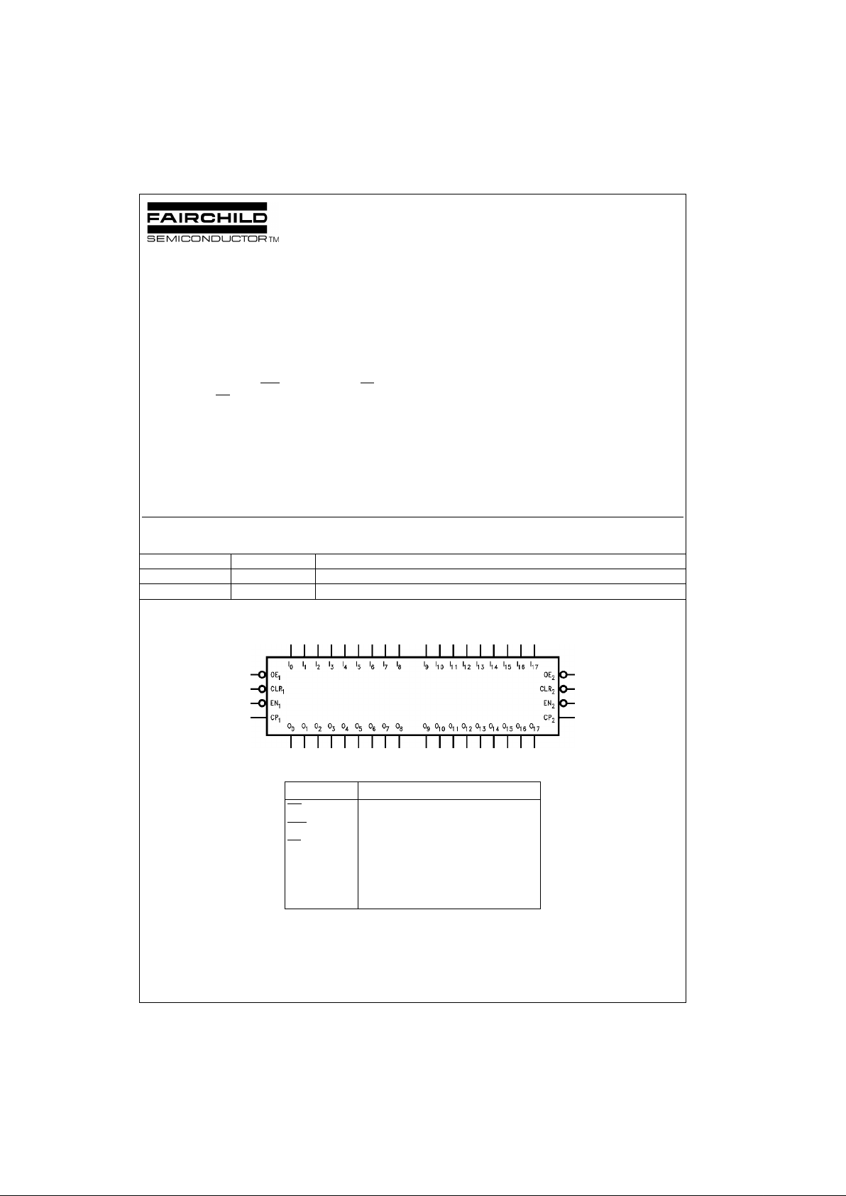
Logic Symbol
Pin Descriptions
FACT, Qui et Series , FACT Quiet Series, an d GTO are trademarks of Fairchild Semiconductor Corporation.
Order Number Package Number Package Description
74ACTQ18823SSC MS56A 56-Lead Shrink Small Outline Package (SSOP), JEDEC MO-118, 0.300” Wide
74ACTQ18823MTD MTD56 56-Lead Thin Shrink Small Outline Package (TSSOP), JEDEC MO-153, 6.1mm Wide
Pin Names Description
OE
n
Output Enable Input (Active LOW)
CLR
n
Clear (Active LOW)
EN
n
Clock Enable (Active LOW)
CP
n
Clock Pulse Input
I
0–I17
Inputs
O
0–O17
Outputs
www.fairchildsemi.com 2
74ACTQ18823
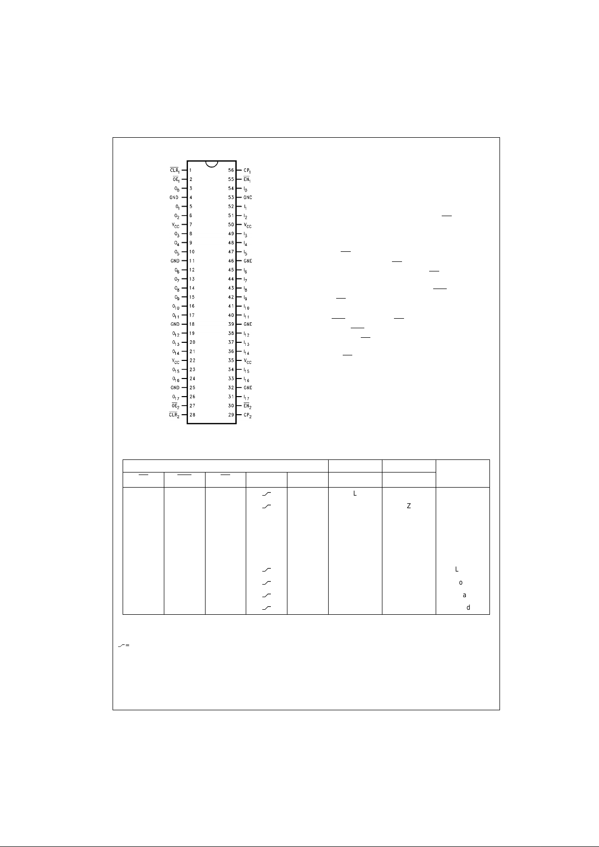
Connection Diagram Functional Description
The ACTQ18823 consists of eighteen D-type edge-triggered flip-flops. These h ave 3-STATE outputs for bus systems organized with inp uts and outpu ts on opposite sides.
The device is byte controlle d with each byte functioning
identically, but independent of the other. The control pins
can be shorted togethe r to ob tain full 16-b it op eration . The
following description applies to each byte. The buffered
clock (CP
n
) and buffered Outpu t Enable (OEn) are com-
mon to all flip-flops within that byte. The flip-flops will store
the state of their indi vidual D inputs that meet set-up and
hold time requir ements on the LOW-to-HIGH CP
n
transi-
tion. With OE
n
LOW, the contents of the flip-flops are avail-
able at the outputs. When OE
n
is HIGH, the outputs go to
the impedance state. Op eration of the OE
n
input does not
affect the state of the flip-flops. In addition to the Clock and
Output Enable pins, there are Clear (CLR
n
) and Clock
Enable (EN
n
) pins. These devices are ide al for parity bus
interfacing in high performance systems.
When CLR
n
is LOW and OEn is LOW, the outputs are
LOW. When CLR
n
is HIGH, data can be entered into the
flip-flops. When EN
n
is LOW, data on the inputs is trans-
ferred to the outputs on the LOW-to-HIGH clock transition.
When the EN
n
is HIGH, the output s do not change state,
regardless of the data or clock input transitions.
Function Table (Note 1)
H= HIGH Voltage Level
L= LOW Voltage Level
X= Immaterial
Z= High Impedance
= LOW-to-HIGH Transition
NC= No Change
Note 1: The table represents t he logic for one byte. The tw o by t es are independent of each other and function ide nt ic ally.
Inputs Internal Output
Function
OE
CLR EN CP I
n
QO
n
HXL
L L Z High Z
HXL
H H Z High Z
HLXXX L Z Clear
LLXXX L L Clear
HHHXX NC Z Hold
LHHXX NC NC Hold
HHL
L L Z Load
HHL
H H Z Load
LHL
L L L Load
LHL
H H H Load
3 www.fairchildsemi.com
74ACTQ18823
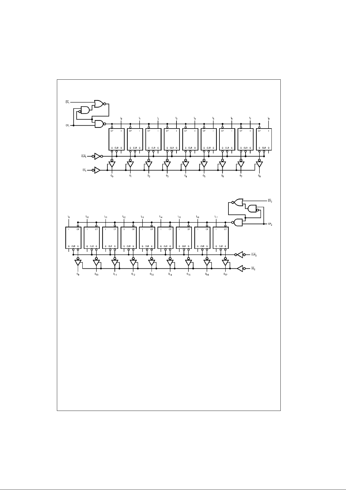
Logic Diagrams
Byte 1 (0:8)
Byte 2 (9:17)
 Loading...