

Fairchild Semiconductor 74ACTQ16646MTD, 74ACTQ16646CW, 74ACTQ16646SSCX, 74ACTQ16646SSC, 74ACTQ16646MTDX Datasheet
June 1991
Revised January 1999
74ACTQ16646 16-Bit Transceiver/Register with 3-STATE Outputs
© 1999 Fairchild Semiconductor Corporation DS010937.prf www.fairchildsemi.com
74ACTQ16646
16-Bit Transceiver/Register with 3-STATE Outputs
General Description
The ACTQ16646 contains sixteen non-inverting bidirectional registered bus transceivers providing multiplexed
transmission of data directl y from th e input bus or fr om the
internal storage r egisters. Each byte has sepa rate control
inputs which can be sho rted toge ther for full 16-bit operation. The DIR inputs dete rmine the direction of data flow
through the device. The CPAB and CPBA inputs load data
into the registers on the LOW-to-HIGH transition. The
ACTQ16646 utilizes Fairchild Quiet Series technology to
guarantee quiet output switching and improved dynamic
threshold performance. FACT Quiet Series features
GTO output control and undershoot corrector for superior
performance.
Features
■ Utilizes Fairchild FACT Quiet Series technology
■ Guaranteed simultaneous switching noise level and
dynamic threshold performance
■ Guaranteed pin-to-pin output skew
■ Independent registers for A and B buses
■ Multiplexed real-time and stored data transfers
■ Separate control logic for each byte
■ 16-bit version of the ACTQ646
■ Outputs source/sink 24 mA
■ Additional specs for Multiple Output Switching
■ Output loading specs for both 50 pF and 250 pF loads
Ordering Code:
Device also available in Tape and Reel. Specify by appendin g s uf f ix let t er “X” to the ordering co de.
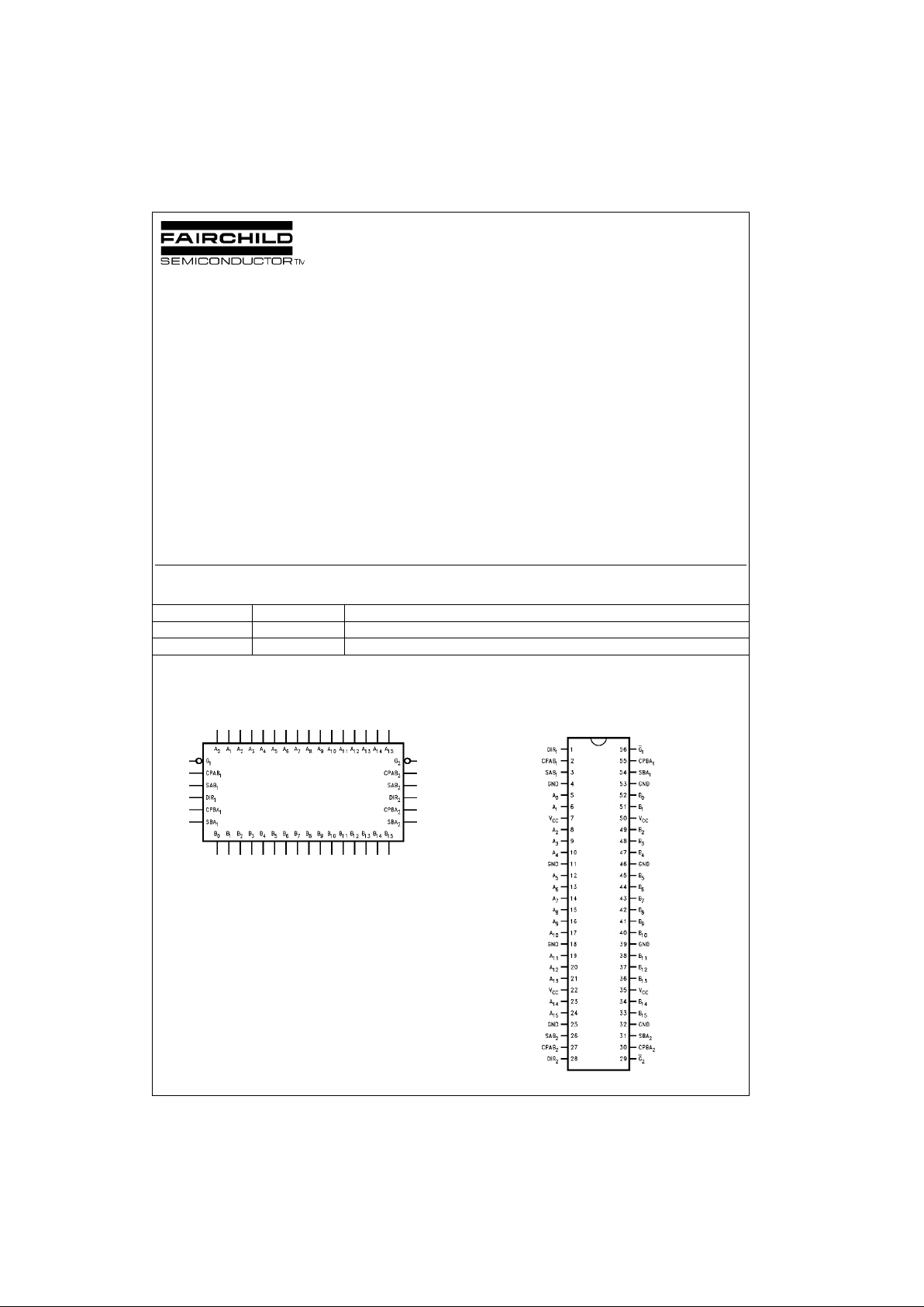
Logic Symbol Connection Diagram
Pin Assignment f or
SSOP and TSSOP
FACT, Quiet Series, FACT Quiet Series and GTO are trademarks of Fairchild Semiconductor Co rporation.
Order Number Package Number Package Description
74ACTQ16646SSC MS56A 56-Lead Shrink Small Outline Package (SSOP), JEDEC MO-118, 0.300” Wide
74ACTQ16646MTD MTD56 56-Lead Thin Shrink Small Outline Package (TSSOP), JEDEC MO-153, 6.1mm Wide
www.fairchildsemi.com 2
74ACTQ16646
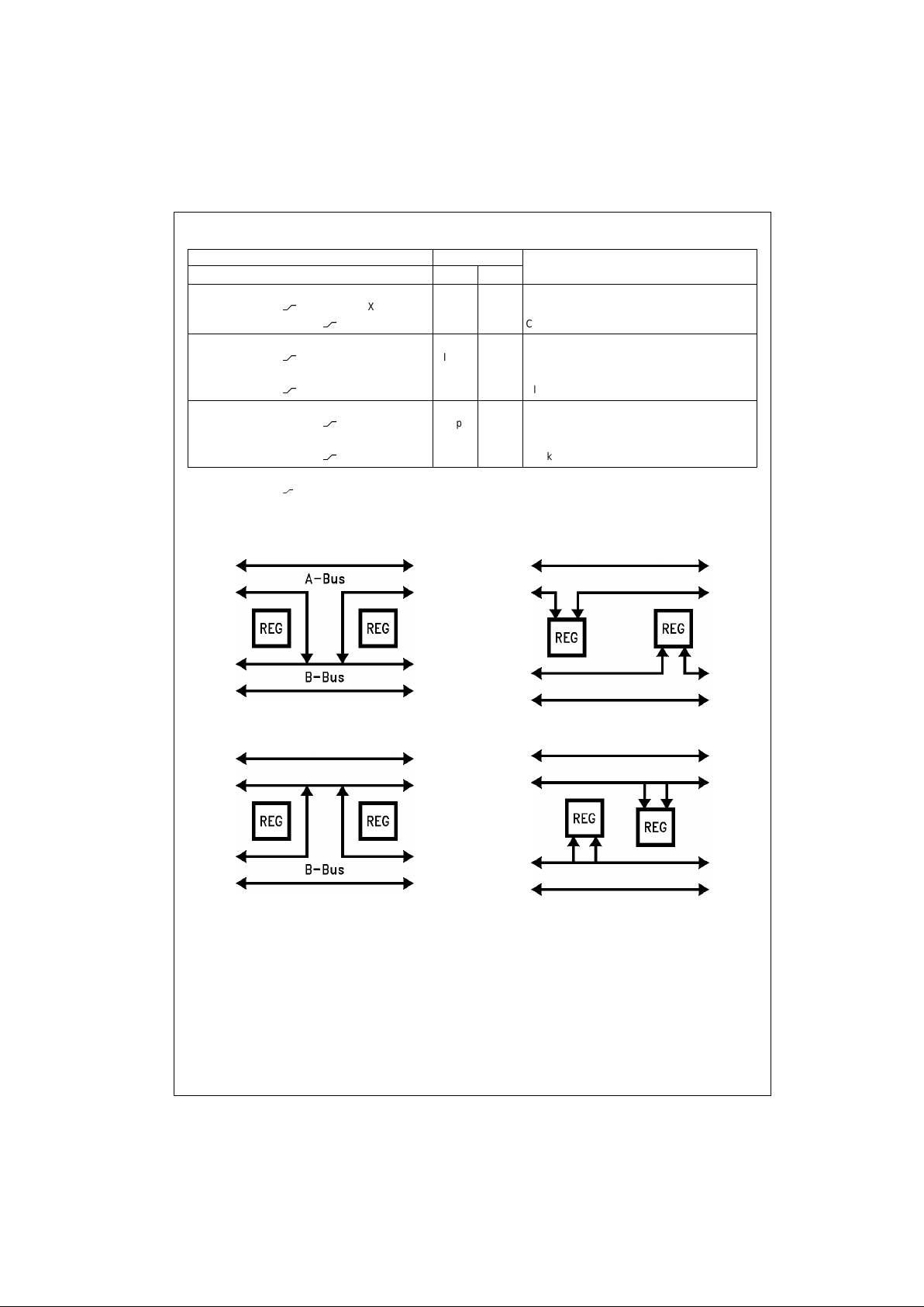
Function Table
H = HIGH Voltage Level X = Immaterial
L = LOW Voltage Level
= LOW-to-HIGH Transition.
Note 1: The data output functions may be enabled or disabled by various signals at the G and DIR inputs. Data input functions are always en abled; i.e., data
at the bus pins will be stored on every LOW-to-HIGH transition of t he appropriate clo ck inputs. Also applies to data I/O (A and B: 8-15) and #2 con t rol pins.
Real Time Transfer
A-Bus to B-Bus
Real Time Transfer
B-Bus to A-Bus
Storage from
Bus to Register
Transfer from
Register to Bus
Inputs Data I/O (Note 1) Output Operation Mode
G
1
DIR1CPAB1CPBA1SAB1SBA1A
0–7
B
0–7
H X H or L H or L X X Isolation
HX
X X X Input Input Clock An Data into A Register
HXX
X X Clock Bn Data Into B Register
LHXXLX An to Bn—Real Time (Transparent Mode)
LH
X L X Input Output Clock An Data to A Register
L H H or L X H X A Register to Bn (Stored Mode)
LH
X H X Clock An Data into A Register and Output to Bn
L L X X X L B n to An—Rea l Time (Transparent Mode)
LLX
X L Output Input Clock Bn Data into B Register
L L X H or L X H B Register to An (Stored Mode)
LLX
X H Clock Bn into B Register and Output to An
3 www.fairchildsemi.com
74ACTQ16646
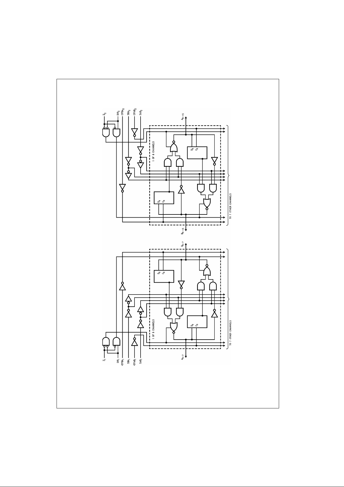
Logic Diagram
 Loading...